US11437331B2 - Chip structure and method for forming the same - Google Patents
Chip structure and method for forming the same Download PDFInfo
- Publication number
- US11437331B2 US11437331B2 US16/655,998 US201916655998A US11437331B2 US 11437331 B2 US11437331 B2 US 11437331B2 US 201916655998 A US201916655998 A US 201916655998A US 11437331 B2 US11437331 B2 US 11437331B2
- Authority
- US
- United States
- Prior art keywords
- conductive
- dielectric layer
- layer
- accordance
- over
- Prior art date
- Legal status (The legal status is an assumption and is not a legal conclusion. Google has not performed a legal analysis and makes no representation as to the accuracy of the status listed.)
- Active, expires
Links
Images


Classifications
-
- H01L24/05—
-
- H—ELECTRICITY
- H10—SEMICONDUCTOR DEVICES; ELECTRIC SOLID-STATE DEVICES NOT OTHERWISE PROVIDED FOR
- H10W—GENERIC PACKAGES, INTERCONNECTIONS, CONNECTORS OR OTHER CONSTRUCTIONAL DETAILS OF DEVICES COVERED BY CLASS H10
- H10W72/00—Interconnections or connectors in packages
- H10W72/01—Manufacture or treatment
- H10W72/012—Manufacture or treatment of bump connectors, dummy bumps or thermal bumps
-
- H—ELECTRICITY
- H10—SEMICONDUCTOR DEVICES; ELECTRIC SOLID-STATE DEVICES NOT OTHERWISE PROVIDED FOR
- H10W—GENERIC PACKAGES, INTERCONNECTIONS, CONNECTORS OR OTHER CONSTRUCTIONAL DETAILS OF DEVICES COVERED BY CLASS H10
- H10W72/00—Interconnections or connectors in packages
- H10W72/90—Bond pads, in general
-
- H01L24/03—
-
- H01L24/13—
-
- H—ELECTRICITY
- H10—SEMICONDUCTOR DEVICES; ELECTRIC SOLID-STATE DEVICES NOT OTHERWISE PROVIDED FOR
- H10W—GENERIC PACKAGES, INTERCONNECTIONS, CONNECTORS OR OTHER CONSTRUCTIONAL DETAILS OF DEVICES COVERED BY CLASS H10
- H10W20/00—Interconnections in chips, wafers or substrates
- H10W20/40—Interconnections external to wafers or substrates, e.g. back-end-of-line [BEOL] metallisations or vias connecting to gate electrodes
- H10W20/41—Interconnections external to wafers or substrates, e.g. back-end-of-line [BEOL] metallisations or vias connecting to gate electrodes characterised by their conductive parts
- H10W20/42—Vias, e.g. via plugs
-
- H—ELECTRICITY
- H10—SEMICONDUCTOR DEVICES; ELECTRIC SOLID-STATE DEVICES NOT OTHERWISE PROVIDED FOR
- H10W—GENERIC PACKAGES, INTERCONNECTIONS, CONNECTORS OR OTHER CONSTRUCTIONAL DETAILS OF DEVICES COVERED BY CLASS H10
- H10W20/00—Interconnections in chips, wafers or substrates
- H10W20/40—Interconnections external to wafers or substrates, e.g. back-end-of-line [BEOL] metallisations or vias connecting to gate electrodes
- H10W20/495—Capacitive arrangements or effects of, or between wiring layers
- H10W20/496—Capacitor integral with wiring layers
-
- H—ELECTRICITY
- H10—SEMICONDUCTOR DEVICES; ELECTRIC SOLID-STATE DEVICES NOT OTHERWISE PROVIDED FOR
- H10W—GENERIC PACKAGES, INTERCONNECTIONS, CONNECTORS OR OTHER CONSTRUCTIONAL DETAILS OF DEVICES COVERED BY CLASS H10
- H10W20/00—Interconnections in chips, wafers or substrates
- H10W20/40—Interconnections external to wafers or substrates, e.g. back-end-of-line [BEOL] metallisations or vias connecting to gate electrodes
- H10W20/497—Inductive arrangements or effects of, or between, wiring layers
-
- H—ELECTRICITY
- H10—SEMICONDUCTOR DEVICES; ELECTRIC SOLID-STATE DEVICES NOT OTHERWISE PROVIDED FOR
- H10W—GENERIC PACKAGES, INTERCONNECTIONS, CONNECTORS OR OTHER CONSTRUCTIONAL DETAILS OF DEVICES COVERED BY CLASS H10
- H10W20/00—Interconnections in chips, wafers or substrates
- H10W20/40—Interconnections external to wafers or substrates, e.g. back-end-of-line [BEOL] metallisations or vias connecting to gate electrodes
- H10W20/498—Resistive arrangements or effects of, or between, wiring layers
-
- H—ELECTRICITY
- H10—SEMICONDUCTOR DEVICES; ELECTRIC SOLID-STATE DEVICES NOT OTHERWISE PROVIDED FOR
- H10W—GENERIC PACKAGES, INTERCONNECTIONS, CONNECTORS OR OTHER CONSTRUCTIONAL DETAILS OF DEVICES COVERED BY CLASS H10
- H10W72/00—Interconnections or connectors in packages
- H10W72/01—Manufacture or treatment
- H10W72/019—Manufacture or treatment of bond pads
-
- H—ELECTRICITY
- H10—SEMICONDUCTOR DEVICES; ELECTRIC SOLID-STATE DEVICES NOT OTHERWISE PROVIDED FOR
- H10W—GENERIC PACKAGES, INTERCONNECTIONS, CONNECTORS OR OTHER CONSTRUCTIONAL DETAILS OF DEVICES COVERED BY CLASS H10
- H10W72/00—Interconnections or connectors in packages
- H10W72/20—Bump connectors, e.g. solder bumps or copper pillars; Dummy bumps; Thermal bumps
-
- H01L2224/02311—
-
- H01L2224/02313—
-
- H01L2224/02331—
-
- H01L2224/03462—
-
- H01L2224/0401—
-
- H01L2224/05548—
-
- H01L2224/13016—
-
- H—ELECTRICITY
- H10—SEMICONDUCTOR DEVICES; ELECTRIC SOLID-STATE DEVICES NOT OTHERWISE PROVIDED FOR
- H10W—GENERIC PACKAGES, INTERCONNECTIONS, CONNECTORS OR OTHER CONSTRUCTIONAL DETAILS OF DEVICES COVERED BY CLASS H10
- H10W20/00—Interconnections in chips, wafers or substrates
- H10W20/01—Manufacture or treatment
- H10W20/071—Manufacture or treatment of dielectric parts thereof
- H10W20/081—Manufacture or treatment of dielectric parts thereof by forming openings in the dielectric parts
- H10W20/083—Manufacture or treatment of dielectric parts thereof by forming openings in the dielectric parts the openings being via holes penetrating underlying conductors
-
- H—ELECTRICITY
- H10—SEMICONDUCTOR DEVICES; ELECTRIC SOLID-STATE DEVICES NOT OTHERWISE PROVIDED FOR
- H10W—GENERIC PACKAGES, INTERCONNECTIONS, CONNECTORS OR OTHER CONSTRUCTIONAL DETAILS OF DEVICES COVERED BY CLASS H10
- H10W70/00—Package substrates; Interposers; Redistribution layers [RDL]
- H10W70/01—Manufacture or treatment
- H10W70/05—Manufacture or treatment of insulating or insulated package substrates, or of interposers, or of redistribution layers
-
- H—ELECTRICITY
- H10—SEMICONDUCTOR DEVICES; ELECTRIC SOLID-STATE DEVICES NOT OTHERWISE PROVIDED FOR
- H10W—GENERIC PACKAGES, INTERCONNECTIONS, CONNECTORS OR OTHER CONSTRUCTIONAL DETAILS OF DEVICES COVERED BY CLASS H10
- H10W70/00—Package substrates; Interposers; Redistribution layers [RDL]
- H10W70/60—Insulating or insulated package substrates; Interposers; Redistribution layers
-
- H—ELECTRICITY
- H10—SEMICONDUCTOR DEVICES; ELECTRIC SOLID-STATE DEVICES NOT OTHERWISE PROVIDED FOR
- H10W—GENERIC PACKAGES, INTERCONNECTIONS, CONNECTORS OR OTHER CONSTRUCTIONAL DETAILS OF DEVICES COVERED BY CLASS H10
- H10W72/00—Interconnections or connectors in packages
- H10W72/01—Manufacture or treatment
- H10W72/019—Manufacture or treatment of bond pads
- H10W72/01931—Manufacture or treatment of bond pads using blanket deposition
- H10W72/01933—Manufacture or treatment of bond pads using blanket deposition in liquid form, e.g. spin coating, spray coating or immersion coating
- H10W72/01935—Manufacture or treatment of bond pads using blanket deposition in liquid form, e.g. spin coating, spray coating or immersion coating by plating, e.g. electroless plating or electroplating
-
- H—ELECTRICITY
- H10—SEMICONDUCTOR DEVICES; ELECTRIC SOLID-STATE DEVICES NOT OTHERWISE PROVIDED FOR
- H10W—GENERIC PACKAGES, INTERCONNECTIONS, CONNECTORS OR OTHER CONSTRUCTIONAL DETAILS OF DEVICES COVERED BY CLASS H10
- H10W72/00—Interconnections or connectors in packages
- H10W72/20—Bump connectors, e.g. solder bumps or copper pillars; Dummy bumps; Thermal bumps
- H10W72/231—Shapes
- H10W72/234—Cross-sectional shape, i.e. in side view
-
- H—ELECTRICITY
- H10—SEMICONDUCTOR DEVICES; ELECTRIC SOLID-STATE DEVICES NOT OTHERWISE PROVIDED FOR
- H10W—GENERIC PACKAGES, INTERCONNECTIONS, CONNECTORS OR OTHER CONSTRUCTIONAL DETAILS OF DEVICES COVERED BY CLASS H10
- H10W72/00—Interconnections or connectors in packages
- H10W72/20—Bump connectors, e.g. solder bumps or copper pillars; Dummy bumps; Thermal bumps
- H10W72/29—Bond pads specially adapted therefor
-
- H—ELECTRICITY
- H10—SEMICONDUCTOR DEVICES; ELECTRIC SOLID-STATE DEVICES NOT OTHERWISE PROVIDED FOR
- H10W—GENERIC PACKAGES, INTERCONNECTIONS, CONNECTORS OR OTHER CONSTRUCTIONAL DETAILS OF DEVICES COVERED BY CLASS H10
- H10W72/00—Interconnections or connectors in packages
- H10W72/90—Bond pads, in general
- H10W72/921—Structures or relative sizes of bond pads
- H10W72/922—Bond pads being integral with underlying chip-level interconnections
Definitions
- FIG. 1A-1 to FIG. 1H-1 are cross-sectional views of various stages of a process for forming a chip structure, in accordance with some embodiments.
- FIG. 1A-2 to FIG. 1C-2 and FIG. 1E-2 to FIG. 1F-2 are top views illustrating the chip structure in FIG. 1A-1 to FIG. 1C-1 and FIG. 1E-1 to FIG. 1F-1 , in accordance with some embodiments.
- FIG. 2A is a cross-sectional view of a chip structure, in accordance with some embodiments.
- FIG. 2B is a top view of the chip structure of FIG. 2A , in accordance with some embodiments.
- FIG. 3A-1 to FIG. 3F-1 are cross-sectional views of various stages of a process for forming a chip structure, in accordance with some embodiments.
- FIG. 3A-2 to FIG. 3E-2 are top views illustrating the chip structure in FIG. 3A-1 to FIG. 3E-1 , in accordance with some embodiments.
- FIG. 4 is a top view of a conductive layer of FIG. 3A-1 , in accordance with some embodiments.
- FIG. 5 is a top view of a conductive layer of FIG. 3A-1 , in accordance with some embodiments.
- FIG. 6 is a top view of a conductive layer of FIG. 3A-1 , in accordance with some embodiments.
- FIG. 7A-1 to FIG. 7F-1 are top views of various stages of a process for forming a chip structure, in accordance with some embodiments.
- FIG. 7A-2 to FIG. 7F-2 are cross-sectional views illustrating the chip structure along a sectional line I-I in FIG. 7A-1 to FIG. 7F-1 , in accordance with some embodiments.
- FIG. 7A-3 to FIG. 7F-3 are cross-sectional views illustrating the chip structure along a sectional line II-II in FIG. 7A-1 to FIG. 7F-1 , in accordance with some embodiments.
- first and second features are formed in direct contact
- additional features may be formed between the first and second features, such that the first and second features may not be in direct contact
- present disclosure may repeat reference numerals and/or letters in the various examples. This repetition is for the purpose of simplicity and clarity and does not in itself dictate a relationship between the various embodiments and/or configurations discussed.
- spatially relative terms such as “beneath,” “below,” “lower,” “above,” “upper” and the like, may be used herein for ease of description to describe one element or feature's relationship to another element(s) or feature(s) as illustrated in the figures.
- the spatially relative terms are intended to encompass different orientations of the device in use or operation in addition to the orientation depicted in the figures.
- the apparatus may be otherwise oriented (rotated 90 degrees or at other orientations) and the spatially relative descriptors used herein may likewise be interpreted accordingly. It should be understood that additional operations can be provided before, during, and after the method, and some of the operations described can be replaced or eliminated for other embodiments of the method.
- FIG. 1A-1 to FIG. 1H-1 are cross-sectional views of various stages of a process for forming a chip structure, in accordance with some embodiments.
- FIG. 1A-2 to FIG. 1C-2 and FIG. 1E-2 to FIG. 1F-2 are top views illustrating the chip structure in FIG. 1A-1 to FIG. 1C-1 and FIG. 1E-1 to FIG. 1F-1 , in accordance with some embodiments.
- the substrate 110 includes, for example, a semiconductor substrate.
- the semiconductor substrate includes, for example, a semiconductor wafer (such as a silicon wafer) or a portion of a semiconductor wafer.
- the substrate 110 is made of an elementary semiconductor material including silicon or germanium in a single crystal, polycrystal, or amorphous structure.
- the substrate 110 is made of a compound semiconductor, such as silicon carbide, gallium arsenide, gallium phosphide, indium phosphide, indium arsenide, an alloy semiconductor, such as SiGe, or GaAsP, or a combination thereof.
- the substrate 110 may also include multi-layer semiconductors, semiconductor on insulator (SOI) (such as silicon on insulator or germanium on insulator), or a combination thereof.
- SOI semiconductor on insulator
- the substrate 110 is a device wafer that includes various device elements.
- the various device elements are formed in and/or over the substrate 110 .
- the device elements are not shown in figures for the purpose of simplicity and clarity. Examples of the various device elements include active devices, passive devices, other suitable elements, or a combination thereof.
- the active devices may include transistors or diodes (not shown) formed at a surface 112 of the substrate 110 .
- the passive devices include resistors, capacitors, or other suitable passive devices.
- the transistors may be metal oxide semiconductor field effect transistors (MOSFET), complementary metal oxide semiconductor (CMOS) transistors, bipolar junction transistors (BJT), high-voltage transistors, high-frequency transistors, p-channel and/or n-channel field effect transistors (PFETs/NFETs), etc.
- MOSFET metal oxide semiconductor field effect transistors
- CMOS complementary metal oxide semiconductor
- BJT bipolar junction transistors
- high-voltage transistors high-frequency transistors
- PFETs/NFETs p-channel and/or n-channel field effect transistors
- PFETs/NFETs p-channel and/or n-channel field effect transistors
- FEOL semiconductor fabrication processes may include deposition, etching, implantation, photolithography, annealing, planarization, one or more other applicable processes, or a combination thereof.
- isolation features are formed in the substrate 110 .
- the isolation features are used to define active regions and electrically isolate various device elements formed in and/or over the substrate 110 in the active regions.
- the isolation features include shallow trench isolation (STI) features, local oxidation of silicon (LOCOS) features, other suitable isolation features, or a combination thereof.
- STI shallow trench isolation
- LOC local oxidation of silicon
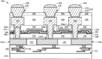
- an interconnect structure 120 is formed over the substrate 110 , in accordance with some embodiments.
- the interconnect structure 120 includes a dielectric structure 122 , wiring layers 124 , and conductive vias 126 , in accordance with some embodiments.
- the dielectric structure 122 may include dielectric layers (not shown) stacked over the substrate 110 , in accordance with some embodiments.
- the wiring layers 124 and the conductive vias 126 are in the dielectric structure 122 , in accordance with some embodiments.
- the wiring layers 124 are spaced apart from each other, in accordance with some embodiments.
- the wiring layers 124 has a thickness T 1 ranging from about 1000 ⁇ to about 4000 ⁇ , in accordance with some embodiments.
- the conductive vias 126 are electrically connected between different wiring layers 124 and between the wiring layer 124 and the device elements (not shown) formed at the surface 112 of the substrate 110 , in accordance with some embodiments.
- the dielectric structure 122 is made of an insulating material, such as oxides (e.g., silicon oxide), nitrides (e.g., silicon nitride or silicon oxynitride), silicon carbide, un-doped silicate glass (USG), or a low-k dielectric material with a k-value lower than that of silicon oxide, in accordance with some embodiments.
- the wiring layers 124 and the conductive vias 126 are made of metal (e.g., copper, aluminum, gold, silver, or tungsten) or alloy thereof, in accordance with some embodiments.
- a dielectric layer 132 and a wiring layer 134 are formed over the interconnect structure 120 , in accordance with some embodiments.
- the wiring layer 134 is formed in the dielectric layer 132 , in accordance with some embodiments.
- the wiring layer 134 is also referred to as a top metal layer, in accordance with some embodiments.
- the wiring layer 134 includes a seed layer 134 a and a conductive layer 134 b , in accordance with some embodiments.
- the conductive layer 134 b is formed over the seed layer 134 a , in accordance with some embodiments.
- the wiring layer 134 includes conductive lines 134 c , 134 d , and 134 e , in accordance with some embodiments.
- the conductive vias 126 are electrically connected between the wiring layer 124 and the wiring layer 134 , in accordance with some embodiments.
- the wiring layer 134 is thicker than each wiring layer 124 , in accordance with some embodiments.
- the wiring layer 134 (or the dielectric layer 132 ) has a thickness T 2 ranging from about 5000 ⁇ to about 13000 ⁇ , in accordance with some embodiments.
- the dielectric structure 132 is made of an insulating material, such as oxides (e.g., silicon oxide), nitrides (e.g., silicon nitride or silicon oxynitride), or un-doped silicate glass (USG), in accordance with some embodiments.
- oxides e.g., silicon oxide
- nitrides e.g., silicon nitride or silicon oxynitride
- USG un-doped silicate glass
- the seed layer 134 a and the conductive layer 134 b are made of metal (e.g., copper, aluminum, gold, silver, or tungsten) or alloy thereof, in accordance with some embodiments.
- the seed layer 134 a is formed using a deposition process, such as a physical vapor deposition process or a chemical vapor deposition process, in accordance with some embodiments.
- the conductive layer 134 b is formed using a plating process, such as an electroplating process, in accordance with some embodiments.
- a barrier layer is formed between the seed layer 134 a and the dielectric layer 132 and between the seed layer 134 a and the dielectric structure 122 .
- the barrier layer is made of nitrides, such as tantalum nitride, in accordance with some embodiments.
- an etch stop layer 140 is formed over the dielectric structure 132 and the wiring layer 134 , in accordance with some embodiments.
- the etch stop layer 140 is thinner than the wiring layer 134 or the dielectric layer 132 , in accordance with some embodiments.
- the etch stop layer 140 has a thickness T 3 ranging from about 400 ⁇ to about 1100 ⁇ , in accordance with some embodiments.
- the etch stop layer 140 is made of nitrides (e.g., silicon nitride or silicon oxynitride), in accordance with some embodiments.
- the etch stop layer 140 is formed using a deposition process, such as a chemical vapor deposition process or a physical vapor deposition process, in accordance with some embodiments.
- a dielectric layer 150 is formed over the etch stop layer 140 , in accordance with some embodiments.
- the dielectric layer 150 is thinner than the wiring layer 134 or the dielectric layer 132 , in accordance with some embodiments.
- the dielectric layer 150 has a thickness T 4 ranging from about 3000 ⁇ to about 5000 ⁇ , in accordance with some embodiments.
- the dielectric layer 150 is made of an insulating material, such as oxides (e.g., silicon oxide), nitrides (e.g., silicon nitride or silicon oxynitride), or un-doped silicate glass (USG), in accordance with some embodiments.
- the dielectric layer 150 is formed using a deposition process, such as a chemical vapor deposition process (e.g., a plasma enhanced chemical vapor deposition (PECVD) process) or a physical vapor deposition process, in accordance with some embodiments.
- a chemical vapor deposition process e.g., a plasma enhanced chemical vapor deposition (PECVD) process
- PECVD plasma enhanced chemical vapor deposition
- a conductive layer 160 is formed over the dielectric layer 150 , in accordance with some embodiments.
- the conductive layer 160 is used as a capacitor electrode, in accordance with some embodiments.
- the conductive layer 160 has an opening 162 , in accordance with some embodiments. The opening 162 exposes a portion of the dielectric layer 150 , in accordance with some embodiments.
- the conductive layer 160 is thinner than the wiring layer 134 , the dielectric layer 132 , or the dielectric layer 150 , in accordance with some embodiments.
- the conductive layer 160 has a thickness T 5 ranging from about 100 ⁇ to about 800 ⁇ , in accordance with some embodiments.
- the thickness T 5 ranges from about 200 ⁇ to about 700 ⁇ , in accordance with some embodiments.
- the conductive layer 160 is made of a capacitor electrode material, in accordance with some embodiments.
- the capacitor electrode material includes metal (e.g., copper, aluminum, gold, silver, or tungsten), alloy thereof, nitrides (e.g., titanium nitride), or another suitable capacitor electrode material, in accordance with some embodiments.
- the conductive layer 160 is formed using a deposition process (e.g., a physical vapor deposition process or a chemical vapor deposition process), a photolithography process, an etching process, and an optional cleaning and passivation process, in accordance with some embodiments.
- the cleaning and passivation process is used to clean the residues from the photolithography process and to passivate the surface of the conductive layer 160 , in accordance with some embodiments.
- the cleaning and passivation process includes a plasma process using N 2 O or Ar as a process gas, in accordance with some embodiments.
- a dielectric layer 170 is formed over the conductive layer 160 and the dielectric layer 150 , in accordance with some embodiments.
- the dielectric layer 170 is used as a capacitor dielectric layer, in accordance with some embodiments.
- the dielectric layer 170 is thinner than the dielectric layer 150 or the conductive layer 160 , in accordance with some embodiments.
- the dielectric layer 170 has a thickness T 6 ranging from about 10 ⁇ to about 200 ⁇ , in accordance with some embodiments.
- the dielectric layer 170 is a single-layered structure. In some other embodiments, the dielectric layer 170 is a multi-layered structure.
- the multi-layered structure has layers, and each layer is made of a material different from that of adjacent layer(s), in accordance with some embodiments.
- the dielectric layer 170 is made of a capacitor dielectric material, such as a high dielectric constant (high-k) material, in accordance with some embodiments.
- the high-k material is made of metal oxides, such as zirconium oxide (ZrO 2 ), hafnium oxide (HfO 2 ), hafnium silicon oxide (HfSiO), hafnium silicon oxynitride (HfSiON), hafnium tantalum oxide (HfTaO), hafnium titanium oxide (HMO), hafnium zirconium oxide (HfZrO), aluminum oxide (Al 2 O 3 ), hafnium dioxide-alumina (HfO 2 —Al 2 O 3 ) alloy, or combinations thereof, in accordance with some embodiments.
- ZrO 2 zirconium oxide
- HfO 2 hafnium oxide
- HfSiO hafnium silicon oxide
- HfSiON hafnium silicon oxynitride
- the high-k material is made of metal nitrides, metal silicates, transition metal-oxides, transition metal-nitrides, transition metal-silicates, oxynitrides of metals, other suitable materials, or combinations thereof.
- the dielectric layer 170 is formed using a deposition process, such as a chemical vapor deposition (CVD) process, a thermal atomic layer deposition (ALD) process, a plasma enhanced atomic layer deposition (PEALD) process, or another suitable deposition process.
- CVD chemical vapor deposition
- ALD thermal atomic layer deposition
- PEALD plasma enhanced atomic layer deposition
- a conductive layer 180 is formed over the dielectric layer 170 , in accordance with some embodiments.
- the conductive layer 180 includes a conductive film 182 and a dummy film 184 , in accordance with some embodiments.
- the conductive film 182 is used as a capacitor electrode, in accordance with some embodiments.
- the conductive film 182 has an opening 182 a , in accordance with some embodiments.
- the opening 182 a exposes a portion of the dielectric layer 170 , in accordance with some embodiments.
- the conductive film 182 partially overlaps the conductive layer 160 , in accordance with some embodiments.
- the conductive film 182 is separated from the conductive layer 160 by the dielectric layer 170 , in accordance with some embodiments.
- the dummy film 184 is used as an etch buffer layer in a subsequent through-hole etching process, in accordance with some embodiments.
- the conductive film 182 and the dummy film 184 are spaced apart from each other, in accordance with some embodiments.
- the conductive film 182 and the dummy film 184 are electrically insulated from each other, in accordance with some embodiments.
- the conductive layer 180 is thinner than the wiring layer 134 , the dielectric layer 132 , or the dielectric layer 150 , in accordance with some embodiments.
- the conductive layer 180 is thicker than the dielectric layer 170 , in accordance with some embodiments.
- the conductive layer 180 has a thickness T 7 ranging from about 100 ⁇ to about 800 ⁇ , in accordance with some embodiments.
- the thickness T 7 ranges from about 200 ⁇ to about 700 ⁇ , in accordance with some embodiments.
- the conductive layer 180 is made of a capacitor electrode material, in accordance with some embodiments.
- the capacitor electrode material includes metal (e.g., copper, aluminum, gold, silver, or tungsten), alloy thereof, nitrides (e.g., titanium nitride), or another suitable capacitor electrode material, in accordance with some embodiments.
- the conductive layer 180 is formed using a deposition process (e.g., a physical vapor deposition process or a chemical vapor deposition process), a photolithography process, an etching process, and an optional cleaning and passivation process, in accordance with some embodiments.
- the cleaning and passivation process is used to clean the residues from the photolithography process and to passivate the surface of the conductive layer 180 , in accordance with some embodiments.
- the cleaning and passivation process includes a plasma process using N 2 O or Ar as a process gas, in accordance with some embodiments.
- a dielectric layer 190 is formed over the conductive layer 180 and the dielectric layer 170 , in accordance with some embodiments.
- the dielectric layer 190 is used as a capacitor dielectric layer, in accordance with some embodiments.
- the dielectric layer 190 is thinner than the dielectric layer 150 or the conductive layer 160 or 180 , in accordance with some embodiments.
- the dielectric layer 190 has a thickness T 8 ranging from about 10 ⁇ to about 200 ⁇ , in accordance with some embodiments.
- the dielectric layer 190 is a single-layered structure. In some other embodiments, the dielectric layer 190 is a multi-layered structure.
- the multi-layered structure has layers, and each layer is made of a material different from that of adjacent layer(s), in accordance with some embodiments.
- the dielectric layer 190 is made of a capacitor dielectric material, such as a high dielectric constant (high-k) material, in accordance with some embodiments.
- the high-k material is made of metal oxides, such as zirconium oxide (ZrO 2 ), hafnium oxide (HfO 2 ), hafnium silicon oxide (HfSiO), hafnium silicon oxynitride (HfSiON), hafnium tantalum oxide (HfTaO), hafnium titanium oxide (HMO), hafnium zirconium oxide (HfZrO), aluminum oxide (Al 2 O 3 ), hafnium dioxide-alumina (HfO 2 —Al 2 O 3 ) alloy, or combinations thereof, in accordance with some embodiments.
- ZrO 2 zirconium oxide
- HfO 2 hafnium oxide
- HfSiO hafnium silicon oxide
- HfSiON hafnium silicon oxynitride
- the high-k material is made of metal nitrides, metal silicates, transition metal-oxides, transition metal-nitrides, transition metal-silicates, oxynitrides of metals, other suitable materials, or combinations thereof.
- the dielectric layer 190 is formed using a deposition process, such as a chemical vapor deposition (CVD) process, a thermal atomic layer deposition (ALD) process, a plasma enhanced atomic layer deposition (PEALD) process, or another suitable deposition process.
- CVD chemical vapor deposition
- ALD thermal atomic layer deposition
- PEALD plasma enhanced atomic layer deposition
- a conductive layer 210 is formed over the dielectric layer 190 , in accordance with some embodiments.
- the conductive layer 210 includes a conductive film 212 and dummy films 214 and 216 , in accordance with some embodiments.
- the conductive film 212 is used as a capacitor electrode, in accordance with some embodiments.
- the conductive film 212 has an opening 212 a , in accordance with some embodiments.
- the opening 212 a exposes a portion of the dielectric layer 190 , in accordance with some embodiments.
- the conductive layer 210 partially overlaps the conductive layer 180 , in accordance with some embodiments.
- the conductive film 212 overlaps the conductive film 182 , in accordance with some embodiments.
- the dummy film 214 overlaps the dummy film 184 , in accordance with some embodiments.
- the conductive layer 210 is separated from the conductive layer 180 by the dielectric layer 190 , in accordance with some embodiments.
- the dummy films 214 and 216 are used as an etch buffer layer in a subsequent through-hole etching process, in accordance with some embodiments.
- the dummy film 216 is in the opening 212 a , in accordance with some embodiments.
- the conductive film 212 and the dummy films 214 and 216 are spaced apart from each other, in accordance with some embodiments.
- the conductive film 212 and the dummy films 214 and 216 are electrically insulated from each other, in accordance with some embodiments.
- the conductive layer 210 is thinner than the wiring layer 134 , the dielectric layer 132 , or the dielectric layer 150 , in accordance with some embodiments.
- the conductive layer 210 is thicker than the dielectric layer 190 , in accordance with some embodiments.
- the conductive layer 210 has a thickness T 9 ranging from about 100 ⁇ to about 800 ⁇ , in accordance with some embodiments.
- the thickness T 9 ranges from about 200 ⁇ to about 700 ⁇ , in accordance with some embodiments.
- the conductive layer 210 is made of a capacitor electrode material, in accordance with some embodiments.
- the capacitor electrode material includes metal (e.g., copper, aluminum, gold, silver, or tungsten), alloy thereof, nitrides (e.g., titanium nitride), or another suitable capacitor electrode material, in accordance with some embodiments.
- the conductive layer 210 is formed using a deposition process (e.g., a physical vapor deposition process or a chemical vapor deposition process), a photolithography process, an etching process, and an optional cleaning and passivation process, in accordance with some embodiments.
- the cleaning and passivation process is used to clean the residues from the photolithography process and to passivate the surface of the conductive layer 210 , in accordance with some embodiments.
- the cleaning and passivation process includes a plasma process using N 2 O or Ar as a process gas, in accordance with some embodiments.
- a dielectric layer 220 is formed over the conductive layer 210 and the dielectric layer 190 , in accordance with some embodiments.
- the dielectric layer 220 is thinner than the wiring layer 134 or the dielectric layer 132 , in accordance with some embodiments.
- the dielectric layer 220 has a thickness T 10 ranging from about 3500 ⁇ to about 5500 ⁇ , in accordance with some embodiments.
- the dielectric layer 220 is made of an insulating material, such as oxides (e.g., silicon oxide), nitrides (e.g., silicon nitride or silicon oxynitride), or un-doped silicate glass (USG), in accordance with some embodiments.
- the dielectric layer 220 is formed using a deposition process, such as a chemical vapor deposition process (e.g., a plasma enhanced chemical vapor deposition process) or a physical vapor deposition process, in accordance with some embodiments.
- FIG. 1E-2 omits the dielectric layer 220 , in accordance with some embodiments.
- portions of the dielectric layer 220 , the conductive layer 210 , the dielectric layer 190 , the conductive layer 180 , the dielectric layer 170 , the conductive layer 160 , the dielectric layer 150 , and the etch stop layer 140 are removed to form through holes 232 , 234 , and 236 , in accordance with some embodiments.
- the through holes 232 , 234 , and 236 respectively expose the conductive lines 134 c , 134 d , and 134 e , in accordance with some embodiments.
- the through hole 232 passes directly through the dummy films 184 and 214 , in accordance with some embodiments.
- the through hole 234 passes directly through the dummy film 216 and the conductive film 182 , in accordance with some embodiments.
- the through hole 236 passes directly through the conductive film 212 and the conductive layer 160 , in accordance with some embodiments.
- the formation of the dummy films 184 , 214 , and 216 helps the through holes 232 , 234 , and 236 pass directly through the same number (i.e., 2 ) of conductive layers 160 , 180 , and 210 . Therefore, the removal process for forming the through holes 232 , 234 , and 236 may be performed uniformly and over etching of the conductive lines 134 c and 134 d may be prevented.
- the through hole 232 directly and passes indirectly through the dielectric layer 220 , the conductive layer 210 , the dielectric layer 190 , the conductive layer 180 , the dielectric layer 170 , the dielectric layer 150 , and the etch stop layer 140 , in accordance with some embodiments.
- the through hole 234 passes indirectly through the conductive layer 160 .
- the through hole 234 directly and passes indirectly through the dielectric layer 220 , the conductive layer 210 , the dielectric layer 190 , the conductive layer 180 , the dielectric layer 170 , the conductive layer 160 , the dielectric layer 150 , and the etch stop layer 140 , in accordance with some embodiments.
- the through hole 236 passes indirectly through the conductive film 182 of the conductive layer 180 , in accordance with some embodiments.
- the through hole 236 directly and passes indirectly through the dielectric layer 220 , the conductive layer 210 , the dielectric layer 190 , the conductive layer 180 , the dielectric layer 170 , the conductive layer 160 , the dielectric layer 150 , and the etch stop layer 140 , in accordance with some embodiments.
- FIG. 1F-2 omits the dielectric layer 220 , in accordance with some embodiments.
- conductive structures 242 , 244 and 246 are respectively formed in and over the through holes 232 , 234 , and 236 , in accordance with some embodiments.
- Each of the conductive structure 242 , 244 , or 246 includes a seed layer 241 a and a conductive layer 241 b , in accordance with some embodiments.
- the conductive layer 241 b is formed over the seed layer 241 a , in accordance with some embodiments.
- the conductive structure 242 includes a conductive via 242 v and a conductive pad 242 p , in accordance with some embodiments.
- the conductive via 242 v is in the through hole 232 , in accordance with some embodiments.
- the conductive via 242 v is electrically connected to the conductive line 134 c , in accordance with some embodiments.
- the conductive pad 242 p is over and in direct contact with the conductive via 242 v , in accordance with some embodiments.
- the conductive structure 244 includes a conductive via 244 v and a conductive pad 244 p , in accordance with some embodiments.
- the conductive via 244 v is in the through hole 234 , in accordance with some embodiments.
- the conductive via 244 v is electrically connected to the conductive film 182 and the conductive line 134 d , in accordance with some embodiments.
- the conductive pad 244 p is over and in direct contact with the conductive via 244 v , in accordance with some embodiments.
- the conductive structure 246 includes a conductive via 246 v and a conductive pad 246 p , in accordance with some embodiments.
- the conductive via 246 v is in the through hole 236 , in accordance with some embodiments.
- the conductive via 246 v is electrically connected to the conductive layer 160 , the conductive film 212 , and the conductive line 134 e , in accordance with some embodiments.
- the conductive film 212 , the dielectric layer 190 , and the conductive film 182 together form a first capacitor, in accordance with some embodiments.
- the conductive layer 160 , the dielectric layer 170 , and the conductive film 182 together form a second capacitor, in accordance with some embodiments.
- the first capacitor is electrically connected in parallel with the second capacitor via the conductive structures 244 and 246 , in accordance with some embodiments.
- the conductive pad 246 p is over and in direct contact with the conductive via 246 v , in accordance with some embodiments.
- the conductive layer 160 , 180 or 210 is thinner than the conductive pad 242 p , 244 p or 246 p , in accordance with some embodiments.
- the conductive pad 242 p , 244 p or 246 p has a thickness T 11 ranging from about 5000 ⁇ to about 11000 ⁇ , in accordance with some embodiments.
- the seed layer 241 a and the conductive layer 241 b are made of metal (e.g., aluminum, copper, gold, silver, or tungsten) or alloy thereof, in accordance with some embodiments.
- the formation of the seed layer 241 a and the conductive layer 241 b includes performing a deposition process to form a seed material layer (not shown); performing a plating process to form a conductive material layer (not shown); and performing a photolithography process and an etching process, in accordance with some embodiments.
- the deposition process includes a physical vapor deposition process or a chemical vapor deposition process, in accordance with some embodiments.
- the plating process includes an electroplating process, in accordance with some embodiments.
- a dielectric layer 250 is formed over the conductive structures 242 , 244 and 246 and the dielectric layer 220 , in accordance with some embodiments.
- the dielectric layer 250 has openings 252 , 254 , and 256 , in accordance with some embodiments.
- the openings 252 , 254 , and 256 respectively expose the conductive structures 242 , 244 and 246 , in accordance with some embodiments.
- the dielectric layer 250 has a thickness T 12 ranging from about 9000 ⁇ to about 15000 ⁇ , in accordance with some embodiments.
- the dielectric layer 250 is made of an insulating material, such as oxides (e.g., silicon oxide), nitrides (e.g., silicon nitride or silicon oxynitride), or un-doped silicate glass (USG), in accordance with some embodiments.
- the dielectric layer 250 is formed using a deposition process, such as a chemical vapor deposition process or a physical vapor deposition process, in accordance with some embodiments.
- a protective layer 260 is formed over the dielectric layer 250 , in accordance with some embodiments.
- the protective layer 260 is used to protect the dielectric layer 250 from damage or being affected by moisture, in accordance with some embodiments.
- the protective layer 260 has openings 262 , 264 , and 266 , in accordance with some embodiments.
- the openings 262 , 264 , and 266 respectively expose the conductive structures 242 , 244 and 246 , in accordance with some embodiments.
- the protective layer 260 has a thickness T 13 ranging from about 3500 ⁇ to about 10000 ⁇ , in accordance with some embodiments.
- the protective layer 260 is made of an insulating material, such as nitrides (e.g., silicon nitride or silicon oxynitride), in accordance with some embodiments.
- the protective layer 260 is formed using a deposition process, such as a chemical vapor deposition process or a physical vapor deposition process, in accordance with some embodiments.
- a seed layer 272 is formed over the protective layer 260 , the dielectric layer 250 , and the conductive structures 242 , 244 and 246 , in accordance with some embodiments.
- the seed layer 272 is made of metal (e.g., copper, aluminum, gold, silver, or tungsten) or alloy thereof, in accordance with some embodiments.
- the seed layer 272 is formed using a deposition process, such as a physical vapor deposition process or a chemical vapor deposition process, in accordance with some embodiments.
- a mask layer 280 is formed over the seed layer 272 , in accordance with some embodiments.
- the mask layer 280 has openings 282 , 284 , and 286 respectively over the openings 262 , 264 , and 266 , in accordance with some embodiments.
- the openings 282 , 284 , and 286 expose portions of the seed layer 272 , in accordance with some embodiments.
- the mask layer 280 is made of a polymer material, such as a photoresist material, in accordance with some embodiments.
- conductive layers 274 are formed over the exposed seed layer 272 and in the openings 282 , 284 , and 286 , in accordance with some embodiments.
- the conductive layers 274 are made of metal (e.g., copper, aluminum, gold, silver, or tungsten) or alloy thereof, in accordance with some embodiments.
- the conductive layers 274 are formed using a plating process, such as an electroplating process, in accordance with some embodiments.
- conductive layers 290 a are formed over the conductive layers 274 , in accordance with some embodiments.
- the conductive layers 290 a are made of a solder material, such as tin, in accordance with some embodiments.
- the conductive layers 290 a are formed using a plating process, such as an electroplating process, in accordance with some embodiments.
- each conductive layer 274 and the seed layer 272 thereunder together form a bump structure 270 , in accordance with some embodiments.
- the bump structure 270 is over and in direct contact with the conductive structure 242 , 244 or 246 , in accordance with some embodiments.
- a reflow process is performed over the conductive layer 290 a to form solder balls 290 , in accordance with some embodiments.
- a chip structure 100 is substantially formed, in accordance with some embodiments.
- the width W 1 of the conductive via 242 v , 244 v or 246 v is greater than the width W 2 of the conductive via 126 of the interconnect structure 120 , in accordance with some embodiments.
- the width W 1 ranges from about ?? ⁇ to about ?? ⁇ , in accordance with some embodiments.
- the width W 2 ranges from about ?? ⁇ to about ?? ⁇ , in accordance with some embodiments. (Note to TSMC inventor: Please provide possible range of the widths W 1 and W 2 , thank you!
- the conductive path between the device elements, which are formed at the surface 112 of the substrate 110 , and the first and second capacitors is greatly reduced, in accordance with some embodiments. Therefore, the resistance of aforementioned conductive path is greatly reduced, in accordance with some embodiments.
- the contact area between the conductive via 242 v , 244 v or 246 v and the first and second capacitors is larger than the contact area between the conductive via 126 and a capacitor (not shown) formed in the interconnect structure 120 . Therefore, the charging speed of the first and second capacitors is improved, and the operation frequency of the first and second capacitors is improved as well, in accordance with some embodiments.
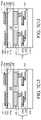
- FIG. 2A is a cross-sectional view of a chip structure 200 , in accordance with some embodiments.
- FIG. 2B is a top view of the chip structure 200 of FIG. 2A , in accordance with some embodiments.
- the chip structure 200 is similar to the chip structure 100 of FIG. 1H-1 , except that the conductive layer 160 of the chip structure 200 further has a dummy film 164 , and the conductive layer 210 of the chip structure 200 does not have the dummy film 216 , in accordance with some embodiments.
- the dummy film 164 is in the opening 162 of the conductive layer 160 , in accordance with some embodiments.
- the conductive structure 244 passes directly through the dummy film 164 of the conductive layer 160 and the conductive film 182 of the conductive layer 180 , in accordance with some embodiments.
- FIG. 3A-1 to FIG. 3F-1 are cross-sectional views of various stages of a process for forming a chip structure, in accordance with some embodiments.
- FIG. 3A-2 to FIG. 3E-2 are top views illustrating the chip structure in FIG. 3A-1 to FIG. 3E-1 , in accordance with some embodiments.
- a step similar to the step of FIG. 1A-1 is performed to form a substrate 110 , an interconnect structure 120 , a dielectric layer 132 , a wiring layer 134 , an etch stop layer 140 , a dielectric layer 150 , and a conductive layer 310 , in accordance with some embodiments.
- the step of FIGS. 3A-1 and 3A-2 is similar to that of the FIGS. 1A-1 and 1A-2 , except that in comparison with the conductive layer 160 formed in the step of FIGS. 1A-1 and 1A-2 , the conductive layer 310 formed in the step of FIGS. 3A-1 and 3A-2 includes a conductive line 312 , and the conductive line 312 has a spiral shape, in accordance with some embodiments.
- the conductive layer 310 is used as an inductor, in accordance with some embodiments.
- the conductive line 312 has end portions 312 a and 312 b and a main portion 312 c , in accordance with some embodiments.
- the end portions 312 a and 312 b are connected to the main portion 312 c , in accordance with some embodiments.
- the end portion 312 a or 312 b is wider than the main portion 312 c , in accordance with some embodiments. That is, a line width W 3 of the end portion 312 a or 312 b is greater than a line width W 4 of the main portion 312 c , in accordance with some embodiments.
- the conductive line 312 may have a round spiral shape (as shown in FIG. 3A-2 ), a square spiral shape (as shown in FIG. 4 ), a hexagonal spiral shape (as shown in FIG. 5 ), or an octagonal spiral shape (as shown in FIG. 6 ), in accordance with some embodiments.
- the conductive layer 310 is made of an inductor material, in accordance with some embodiments.
- the inductor material includes metal (e.g., copper, aluminum, gold, silver, or tungsten), alloy thereof, nitrides (e.g., titanium nitride), or another suitable inductor material, in accordance with some embodiments.
- a dielectric layer 320 is formed over the conductive layer 310 and the dielectric layer 150 , in accordance with some embodiments.
- the dielectric layer 320 conformally covers the conductive layer 310 , in accordance with some embodiments.
- the dielectric layer 320 is a single-layered structure.
- the dielectric layer 320 is a multi-layered structure.
- the multi-layered structure has layers, and each layer is made of a material different from that of adjacent layer(s), in accordance with some embodiments.
- the dielectric layer 320 is made of an insulating material, such as oxides (e.g., silicon oxide), nitrides (e.g., silicon nitride or silicon oxynitride), silicon carbide, un-doped silicate glass (USG), or a low-k dielectric material with a k-value lower than that of silicon oxide, in accordance with some embodiments.
- the dielectric layer 320 is formed using a deposition process, such as a chemical vapor deposition (CVD) process, a thermal atomic layer deposition (ALD) process, a plasma enhanced atomic layer deposition (PEALD) process, or another suitable deposition process.
- CVD chemical vapor deposition
- ALD thermal atomic layer deposition
- PEALD plasma enhanced atomic layer deposition
- a conductive layer 330 is formed over the dielectric layer 320 , in accordance with some embodiments.
- the conductive layer 330 includes a conductive line 332 , and the conductive line 332 has a spiral shape, in accordance with some embodiments.
- the conductive layer 330 is used as an inductor, in accordance with some embodiments.
- the conductive line 332 has end portions 332 a and 332 b and a main portion 332 c , in accordance with some embodiments.
- the end portions 332 a and 332 b are connected to the main portion 332 c , in accordance with some embodiments.
- the end portion 332 a or 332 b is wider than the main portion 332 c , in accordance with some embodiments. That is, a line width W 5 of the end portion 332 a or 332 b is greater than a line width W 6 of the main portion 332 c , in accordance with some embodiments.
- the conductive line 332 may have a round spiral shape (as shown in FIG. 3B-2 ), a square spiral shape (which is similar to that of the conductive line 312 of FIG. 4 ), a hexagonal spiral shape (which is similar to that of the conductive line 312 of FIG. 5 ), or an octagonal spiral shape (which is similar to that of the conductive line 312 of FIG. 6 ), in accordance with some embodiments.
- the conductive layer 330 is made of an inductor material, in accordance with some embodiments.
- the inductor material includes metal (e.g., copper, aluminum, gold, silver, or tungsten), alloy thereof, nitrides (e.g., titanium nitride), or another suitable inductor material, in accordance with some embodiments.
- a dielectric layer 340 is formed over the conductive layer 330 and the dielectric layer 320 , in accordance with some embodiments.
- the dielectric layer 340 conformally covers the conductive layer 330 and the dielectric layer 320 , in accordance with some embodiments.
- the dielectric layer 340 is a single-layered structure. In some other embodiments, the dielectric layer 340 is a multi-layered structure.
- the multi-layered structure has layers, and each layer is made of a material different from that of adjacent layer(s), in accordance with some embodiments.
- the dielectric layer 340 is made of an insulating material, such as oxides (e.g., silicon oxide), nitrides (e.g., silicon nitride or silicon oxynitride), silicon carbide, un-doped silicate glass (USG), or a low-k dielectric material with a k-value lower than that of silicon oxide, in accordance with some embodiments.
- oxides e.g., silicon oxide
- nitrides e.g., silicon nitride or silicon oxynitride
- silicon carbide silicon carbide
- un-doped silicate glass (USG) un-doped silicate glass
- a low-k dielectric material with a k-value lower than that of silicon oxide
- the dielectric layer 340 is formed using a deposition process, such as a chemical vapor deposition (CVD) process, a thermal atomic layer deposition (ALD) process, a plasma enhanced atomic layer deposition (PEALD) process, or another suitable deposition process.
- CVD chemical vapor deposition
- ALD thermal atomic layer deposition
- PEALD plasma enhanced atomic layer deposition
- a conductive layer 350 is formed over the dielectric layer 340 , in accordance with some embodiments.
- the conductive layer 350 includes a conductive line 352 , and the conductive line 352 has a spiral shape, in accordance with some embodiments.
- the conductive layer 350 is used as an inductor, in accordance with some embodiments.
- the conductive line 352 has end portions 352 a and 352 b and a main portion 352 c , in accordance with some embodiments.
- the end portions 352 a and 352 b are connected to the main portion 352 c , in accordance with some embodiments.
- the end portion 352 a or 352 b is wider than the main portion 352 c , in accordance with some embodiments. That is, a line width W 7 of the end portion 352 a or 352 b is greater than a line width W 8 of the main portion 352 c , in accordance with some embodiments.
- the conductive line 352 may have a round spiral shape (as shown in FIG. 3C-2 ), a square spiral shape (which is similar to that of the conductive line 312 of FIG. 4 ), a hexagonal spiral shape (which is similar to that of the conductive line 312 of FIG. 5 ), or an octagonal spiral shape (which is similar to that of the conductive line 312 of FIG. 6 ), in accordance with some embodiments.
- the conductive layer 350 is made of an inductor material, in accordance with some embodiments.
- the inductor material includes metal (e.g., copper, aluminum, gold, silver, or tungsten), alloy thereof, nitrides (e.g., titanium nitride), or another suitable inductor material, in accordance with some embodiments.
- the step of FIG. 1D-1 is performed to form a dielectric layer 220 over the conductive layer 350 and the dielectric layer 340 , in accordance with some embodiments.
- the dielectric layer 220 covers the entire conductive layer 350 and the entire dielectric layer 340 , in accordance with some embodiments.
- FIG. 3D-2 omits the dielectric layer 220 , in accordance with some embodiments.
- portions of the dielectric layer 220 , the conductive layer 350 , the dielectric layer 340 , the conductive layer 330 , the dielectric layer 320 , the conductive layer 310 , the dielectric layer 150 , and the etch stop layer 140 are removed to form through holes 362 and 364 , in accordance with some embodiments.
- the through holes 362 and 364 respectively expose the conductive lines 134 c and 134 d , in accordance with some embodiments.
- the through hole 362 passes through the end portions 312 a , 332 a , and 352 a , in accordance with some embodiments.
- the through hole 364 passes through the end portions 312 b , 332 b , and 352 b , in accordance with some embodiments.
- the through holes 362 and 364 are formed using a photolithography process and an etching process, in accordance with some embodiments.
- FIG. 3E-2 omits the dielectric layer 220 , in accordance with some embodiments.
- the step of FIG. 1F-1 is performed to form conductive structures 242 and 244 , in accordance with some embodiments.
- the conductive structures 242 and 244 are respectively formed in and over the through holes 362 and 364 , in accordance with some embodiments.
- Each of the conductive structure 242 or 244 includes a seed layer 241 a and a conductive layer 241 b , in accordance with some embodiments.
- the conductive layer 241 b is formed over the seed layer 241 a , in accordance with some embodiments.
- the conductive structure 242 includes a conductive via 242 v and a conductive pad 242 p , in accordance with some embodiments.
- the conductive via 242 v is in the through hole 362 , in accordance with some embodiments.
- the conductive via 242 v passes through the end portions 312 a , 332 a , and 352 a , in accordance with some embodiments.
- the conductive via 242 v is electrically connected to the conductive layers 310 , 330 , and 350 , in accordance with some embodiments.
- the conductive pad 242 p is over and in direct contact with the conductive via 242 v , in accordance with some embodiments.
- the conductive structure 244 includes a conductive via 244 v and a conductive pad 244 p , in accordance with some embodiments.
- the conductive via 244 v is in the through hole 364 , in accordance with some embodiments.
- the conductive via 244 v passes through the end portions 312 b , 332 b , and 352 b , in accordance with some embodiments.
- the conductive via 244 v is electrically connected to the conductive layers 310 , 330 , and 350 , in accordance with some embodiments.
- the conductive pad 244 p is over and in direct contact with the conductive via 244 v , in accordance with some embodiments.
- the conductive layer 310 is a first inductor
- the conductive layer 330 is a second inductor
- the conductive layer 350 is a third inductor.
- the first inductor, the second inductor and the third inductor are electrically connected in parallel with each other via the conductive structures 242 and 244 , in accordance with some embodiments.
- the steps of FIGS. 1G-1 and 1H-1 are performed to form a dielectric layer 250 , a protective layer 260 , bump structures 270 , and solder balls 290 , in accordance with some embodiments.
- the dielectric layer 250 is formed over the conductive structures 242 and 244 and the dielectric layer 220 , in accordance with some embodiments.
- the dielectric layer 250 has openings 252 and 254 , in accordance with some embodiments.
- the openings 252 and 254 respectively expose the conductive structures 242 and 244 , in accordance with some embodiments.
- the protective layer 260 is formed over the dielectric layer 250 , in accordance with some embodiments.
- the protective layer 260 is used to protect the dielectric layer 250 from damage or being affected by moisture, in accordance with some embodiments.
- the protective layer 260 has openings 262 and 264 , in accordance with some embodiments. The openings 262 and 264 respectively expose the conductive structures 242 and 244 , in accordance with some embodiments.
- the bump structures 270 are respectively in the openings 262 and 264 , in accordance with some embodiments.
- Each bump structure 270 includes a seed layer 272 and a conductive layer 274 , in accordance with some embodiments.
- the conductive layer 274 is over the seed layer 272 , in accordance with some embodiments.
- the solder balls 290 are respectively over the bump structures 270 , in accordance with some embodiments.
- a chip structure 300 is substantially formed, in accordance with some embodiments.
- the width W 1 of the conductive via 242 v or 244 v is greater than the width W 2 of the conductive via 126 of the interconnect structure 120 , in accordance with some embodiments.
- the conductive path between the device elements, which are formed at the surface 112 of the substrate 110 , and the first, second and third inductors is greatly reduced, in accordance with some embodiments. Therefore, the resistance of aforementioned conductive path is greatly reduced, in accordance with some embodiments.
- the contact area between the conductive via 242 v or 244 v and the first, second and third inductors is larger than the contact area between the conductive via 126 and an inductor (not shown) formed in the interconnect structure 120 . Therefore, the resistance between the conductive via 242 v or 244 v and the first, second and third inductors is reduced, in accordance with some embodiments.
- FIG. 7A-1 to FIG. 7F-1 are top views of various stages of a process for forming a chip structure, in accordance with some embodiments.
- FIG. 7A-2 to FIG. 7F-2 are cross-sectional views illustrating the chip structure along a sectional line I-I in FIG. 7A-1 to FIG. 7F-1 , in accordance with some embodiments.
- FIG. 7A-3 to FIG. 7F-3 are cross-sectional views illustrating the chip structure along a sectional line II-II in FIG. 7A-1 to FIG. 7F-1 , in accordance with some embodiments.
- a step similar to the step of FIG. 1A-1 is performed to form a substrate 110 , an interconnect structure 120 , a dielectric layer 132 , a wiring layer 134 , an etch stop layer 140 , a dielectric layer 150 , and a conductive layer 710 , in accordance with some embodiments.
- the wiring layer 134 includes conductive lines 134 c , 134 d , 134 e , and 134 f , in accordance with some embodiments.
- the step of FIGS. 7A-1, 7A-2, and 7A-3 is similar to the FIGS. 1A-1 and 1A-2 , except that in comparison with the conductive layer 160 formed in the step of FIGS. 1A-1 and 1A-2 , the conductive layer 710 formed in the step of FIGS. 7A-1, 7A-2, and 7A-3 includes a conductive line 712 , in accordance with some embodiments.
- the conductive line 712 has a wavy shape (or a meander shape), in accordance with some embodiments.
- the conductive line 712 is used as a resistor, in accordance with some embodiments.
- the conductive line 712 has end portions 712 a and 712 b and a main portion 712 c , in accordance with some embodiments.
- the end portions 712 a and 712 b are connected to the main portion 712 c , in accordance with some embodiments.
- the end portion 712 a or 712 b is wider than the main portion 712 c , in accordance with some embodiments. That is, a line width W 9 of the end portion 712 a or 712 b is greater than a line width W 10 of the main portion 712 c , in accordance with some embodiments.
- the conductive layer 710 is made of a resistor material, in accordance with some embodiments.
- the resistor material includes semiconductor (e.g., polysilicon), nitrides (e.g., titanium nitride), metal (e.g., tantalum), alloy (e.g., nichrome) or another suitable resistor material, in accordance with some embodiments.
- the resistance of the resistor material is higher than that of the materials of the wiring layers 124 and 134 or the conductive vias 126 .
- the conductive layer 710 and the wiring layers 124 and 134 are made of the same material (e.g., copper, aluminum, gold, silver, tungsten, alloys thereof), and the resistance of the conductive layer 710 may be adjusted by adjusting the shape or the size (e.g., the length) of the conductive line 712 , in accordance with some embodiments.
- a dielectric layer 720 is formed over the conductive layer 710 and the dielectric layer 150 , in accordance with some embodiments.
- the dielectric layer 720 covers the entire conductive layer 710 and the entire dielectric layer 150 , in accordance with some embodiments.
- the dielectric layer 720 conformally covers the conductive layer 710 and the dielectric layer 150 , in accordance with some embodiments.
- the dielectric layer 720 is a single-layered structure.
- the dielectric layer 720 is a multi-layered structure.
- the multi-layered structure has layers, and each layer is made of a material different from that of adjacent layer(s), in accordance with some embodiments.
- the dielectric layer 720 is made of an insulating material, such as oxides (e.g., silicon oxide), nitrides (e.g., silicon nitride or silicon oxynitride), silicon carbide, un-doped silicate glass (USG), or a low-k dielectric material with a k-value lower than that of silicon oxide, in accordance with some embodiments.
- oxides e.g., silicon oxide
- nitrides e.g., silicon nitride or silicon oxynitride
- silicon carbide silicon carbide
- un-doped silicate glass (USG) un-doped silicate glass
- a low-k dielectric material with a k-value lower than that of silicon oxide
- the dielectric layer 720 is formed using a deposition process, such as a chemical vapor deposition (CVD) process, a thermal atomic layer deposition (ALD) process, a plasma enhanced atomic layer deposition (PEALD) process, or another suitable deposition process.
- CVD chemical vapor deposition
- ALD thermal atomic layer deposition
- PEALD plasma enhanced atomic layer deposition
- a conductive layer 730 is formed over the dielectric layer 720 , in accordance with some embodiments.
- the conductive layer 730 includes a conductive line 732 and dummy films 734 and 736 , in accordance with some embodiments.
- the conductive line 732 has a wavy shape (or a meander shape), in accordance with some embodiments.
- the conductive line 732 is used as a resistor, in accordance with some embodiments.
- the conductive line 732 has end portions 732 a and 732 b and a main portion 732 c , in accordance with some embodiments.
- the end portions 732 a and 732 b are connected to the main portion 732 c , in accordance with some embodiments.
- the end portion 732 a or 732 b is wider than the main portion 732 c , in accordance with some embodiments. That is, a line width W 11 of the end portion 732 a or 732 b is greater than a line width W 12 of the main portion 732 c , in accordance with some embodiments.
- the dummy film 734 overlaps the end portion 712 a , in accordance with some embodiments.
- the end portion 732 b overlaps the end portion 712 b , in accordance with some embodiments.
- the conductive layer 730 is made of a resistor material, in accordance with some embodiments.
- the resistor material includes semiconductor (e.g., polysilicon), nitrides (e.g., titanium nitride), metal (e.g., tantalum), alloy (e.g., nichrome), or another suitable resistor material, in accordance with some embodiments.
- the resistance of the resistor material is higher than that of the materials of the wiring layers 124 and 134 or the conductive vias 126 .
- the conductive layer 730 and the wiring layers 124 and 134 are made of the same material (e.g., copper, aluminum, gold, silver, tungsten, alloys thereof), and the resistance of the conductive layer 730 may be adjusted by adjusting the shape or the size (e.g., the length) of the conductive line 732 , in accordance with some embodiments.
- a dielectric layer 740 is formed over the conductive layer 730 and the dielectric layer 720 , in accordance with some embodiments.
- the dielectric layer 740 covers the entire conductive layer 730 and the entire dielectric layer 720 , in accordance with some embodiments.
- the dielectric layer 740 conformally covers the conductive layer 730 and the dielectric layer 720 , in accordance with some embodiments.
- the dielectric layer 740 is a single-layered structure.
- the dielectric layer 740 is a multi-layered structure.
- the multi-layered structure has layers, and each layer is made of a material different from that of adjacent layer(s), in accordance with some embodiments.
- the dielectric layer 740 is made of an insulating material, such as oxides (e.g., silicon oxide), nitrides (e.g., silicon nitride or silicon oxynitride), silicon carbide, un-doped silicate glass (USG), or a low-k dielectric material with a k-value lower than that of silicon oxide, in accordance with some embodiments.
- the dielectric layer 740 is formed using a deposition process, such as a chemical vapor deposition (CVD) process, a thermal atomic layer deposition (ALD) process, a plasma enhanced atomic layer deposition (PEALD) process, or another suitable deposition process.
- CVD chemical vapor deposition
- ALD thermal atomic layer deposition
- PEALD plasma enhanced atomic layer deposition
- a conductive layer 750 is formed over the dielectric layer 740 , in accordance with some embodiments.
- the conductive layer 750 includes a conductive line 752 , in accordance with some embodiments.
- the conductive line 752 has a wavy shape (or a meander shape), in accordance with some embodiments.
- the conductive line 752 is used as a resistor, in accordance with some embodiments.
- the conductive line 752 has end portions 752 a and 752 b and a main portion 752 c , in accordance with some embodiments.
- the end portions 752 a and 752 b are connected to the main portion 752 c , in accordance with some embodiments.
- the end portion 752 a or 752 b is wider than the main portion 752 c , in accordance with some embodiments. That is, a line width W 13 of the end portion 752 a or 752 b is greater than a line width W 14 of the main portion 752 c , in accordance with some embodiments.
- the conductive layer 750 is made of a resistor material, in accordance with some embodiments.
- the resistor material includes semiconductor (e.g., polysilicon), nitrides (e.g., titanium nitride), metal (e.g., tantalum), alloy (e.g., nichrome), or another suitable resistor material, in accordance with some embodiments.
- the resistance of the resistor material is higher than that of the materials of the wiring layers 124 and 134 or the conductive vias 126 .
- the conductive layer 750 and the wiring layers 124 and 134 are made of the same material (e.g., copper, aluminum, gold, silver, tungsten, alloys thereof), and the resistance of the conductive layer 750 may be adjusted by adjusting the shape or the size (e.g., the length) of the conductive line 752 , in accordance with some embodiments.
- FIGS. 7D-1, 7D-2, and 7D-3 the step of FIG. 1D-1 is performed to form a dielectric layer 220 over the conductive layer 750 and the dielectric layer 740 , in accordance with some embodiments.
- FIG. 7D-1 omits the dielectric layer 220 , in accordance with some embodiments.
- portions of the dielectric layer 220 , the conductive layer 750 , the dielectric layer 740 , the conductive layer 730 , the dielectric layer 720 , the conductive layer 710 , the dielectric layer 150 , and the etch stop layer 140 are removed to form through holes 762 , 764 , 766 and 768 , in accordance with some embodiments.
- the through holes 762 , 764 , 766 and 768 respectively expose the conductive lines 134 c , 134 d , 134 e and 134 f , in accordance with some embodiments.
- the through hole 762 passes through the end portion 712 a and the dummy film 734 , in accordance with some embodiments.
- the through hole 764 passes through the end portions 732 a and 752 a , in accordance with some embodiments.
- the through hole 766 passes through the end portions 712 b and 732 b , in accordance with some embodiments.
- the through hole 768 passes through the end portion 752 b and the dummy film 736 , in accordance with some embodiments.
- the through holes 762 , 764 , 766 and 768 are formed using a photolithography process and an etching process, in accordance with some embodiments.
- FIG. 7E-1 omits the dielectric layer 220 , in accordance with some embodiments.
- the step of FIG. 1F-1 is performed to form conductive structures 242 , 244 , 246 and 248 , in accordance with some embodiments.
- the conductive structures 242 , 244 , 246 and 248 are respectively formed in and over the through holes 762 , 764 , 766 and 768 , in accordance with some embodiments.
- Each of the conductive structure 242 , 244 , 246 or 248 includes a seed layer 241 a and a conductive layer 241 b , in accordance with some embodiments.
- the conductive layer 241 b is formed over the seed layer 241 a , in accordance with some embodiments.
- the conductive structure 242 includes a conductive via 242 v and a conductive pad 242 p , in accordance with some embodiments.
- the conductive via 242 v is in the through hole 762 , in accordance with some embodiments.
- the conductive via 242 v passes through the end portion 712 a and the dummy film 734 , in accordance with some embodiments.
- the conductive via 242 v is electrically connected to the conductive line 712 , in accordance with some embodiments.
- the conductive pad 242 p is over and in direct contact with the conductive via 242 v , in accordance with some embodiments.
- the conductive structure 244 includes a conductive via 244 v and a conductive pad 244 p , in accordance with some embodiments.
- the conductive via 244 v is in the through hole 764 , in accordance with some embodiments.
- the conductive via 244 v passes through the end portions 732 a and 752 a , in accordance with some embodiments.
- the conductive via 244 v is electrically connected to the conductive lines 732 and 752 , in accordance with some embodiments.
- the conductive pad 244 p is over and in direct contact with the conductive via 244 v , in accordance with some embodiments.
- the conductive structure 246 includes a conductive via 246 v and a conductive pad 246 p , in accordance with some embodiments.
- the conductive via 246 v is in the through hole 766 , in accordance with some embodiments.
- the conductive via 246 v passes through the end portions 712 b and 732 b , in accordance with some embodiments.
- the conductive via 246 v is electrically connected to the conductive lines 712 and 732 , in accordance with some embodiments.
- the conductive pad 246 p is over and in direct contact with the conductive via 246 v , in accordance with some embodiments.
- the conductive structure 248 includes a conductive via 248 v and a conductive pad 248 p , in accordance with some embodiments.
- the conductive via 248 v is in the through hole 768 , in accordance with some embodiments.
- the conductive via 248 v passes through the end portion 752 b and the dummy film 736 , in accordance with some embodiments.
- the conductive via 248 v is electrically connected to the conductive line 752 , in accordance with some embodiments.
- the conductive pad 248 p is over and in direct contact with the conductive via 248 v , in accordance with some embodiments.
- the conductive line 712 is a first resistor
- the conductive line 732 is a second resistor
- the conductive line 752 is a third resistor.
- the first resistor, the second resistor and the third resistor are electrically connected in series with each other via the conductive structures 242 , 244 , 246 and 248 , in accordance with some embodiments.
- a current flows from the conductive structure 242 to the conductive structure 248 sequentially through the conductive line 712 (including the end portion 712 a , the main portion 712 c , and the end portion 712 b ), the conductive structure 246 , the conductive line 732 (including the end portion 732 b , the main portion 732 c , and the end portion 732 a ), the conductive structure 244 , and the conductive line 752 (including the end portion 752 a , the main portion 752 c , and the end portion 752 b ), in accordance with some embodiments.
- the steps of FIGS. 1G-1 and 1H-1 are performed to form a dielectric layer 250 , a protective layer 260 , bump structures 270 , and solder balls 290 , in accordance with some embodiments.
- the dielectric layer 250 is formed over the conductive structures 242 , 244 , 246 and 248 and the dielectric layer 220 , in accordance with some embodiments.
- the dielectric layer 250 has openings 252 , 254 , 256 and 258 , in accordance with some embodiments.
- the openings 252 , 254 , 256 and 258 respectively expose the conductive structures 242 , 244 , 246 and 248 , in accordance with some embodiments.
- the protective layer 260 is formed over the dielectric layer 250 , in accordance with some embodiments.
- the protective layer 260 is used to protect the dielectric layer 250 from damage or being affected by moisture, in accordance with some embodiments.
- the protective layer 260 has openings 262 , 264 , 266 and 268 , in accordance with some embodiments.
- the openings 262 , 264 , 266 and 268 respectively expose the conductive structures 242 , 244 , 246 and 248 , in accordance with some embodiments.
- the bump structures 270 are respectively formed in the openings 262 , 264 , 266 and 268 , in accordance with some embodiments.
- Each bump structure 270 includes a seed layer 272 and a conductive layer 274 , in accordance with some embodiments.
- the conductive layer 274 is over the seed layer 272 , in accordance with some embodiments.
- the solder balls 290 are respectively over the bump structures 270 , in accordance with some embodiments.
- a chip structure 700 is substantially formed, in accordance with some embodiments.
- the conductive path between the device elements, which are formed at the surface 112 of the substrate 110 , and the first, second and third resistors may be precisely controlled which may prevent undesired resistance, in accordance with some embodiments. Therefore, the performance of the chip structure 700 is improved, in accordance with some embodiments.
- the thickness of the conductive layer 310 , 330 , 350 , 710 , 730 or 750 is substantially similar to or the same as that of the conductive layer 160 (as shown in FIG. 1H-1 ), in accordance with some embodiments.
- the thickness of the dielectric layer 320 , 340 , 720 or 740 is substantially similar to or the same as that of the dielectric layer 170 or 190 (as shown in FIG. 1H-1 ), in accordance with some embodiments.
- Processes and materials for forming the chip structures 200 , 300 and 700 may be similar to, or the same as, those for forming the chip structure 100 described above.
- chip structures and methods for forming the same are provided.
- the methods (for forming the chip structure) form a passive device between a conductive pad and a top metal layer of a chip structure, in accordance with some embodiments.
- the passive device is electrically connected to a conductive via between the conductive pad and the top metal layer, in accordance with some embodiments. Since the passive device is integrated into the chip structure, the conductive path between the passive device and device elements formed in the chip structure is reduced, which reduces the resistance of the conductive path. Therefore, the performance of the chip structure is improved.
- a chip structure includes a semiconductor substrate.
- the chip structure includes a first dielectric layer over the semiconductor substrate.
- the chip structure includes a first conductive layer over the first dielectric layer.
- the chip structure includes a second dielectric layer over the first conductive layer and the first dielectric layer.
- the chip structure includes a first conductive via passing through the second dielectric layer, the first conductive layer, and the first dielectric layer and electrically connected to the first conductive layer.
- the chip structure includes a second conductive via passing through the second dielectric layer and the first dielectric layer.
- the first conductive layer is partially between the first conductive via and the second conductive via.
- the chip structure includes a first conductive pad over and in direct contact with the first conductive via.
- the chip structure includes a second conductive pad over and in direct contact with the second conductive via.
- a chip structure includes a semiconductor substrate.
- the chip structure includes a conductive line over the semiconductor substrate.
- the chip structure includes a first dielectric layer over the conductive line and the semiconductor substrate.
- the chip structure includes a first conductive layer over the first dielectric layer.
- the first conductive layer is thinner than the conductive line.
- the chip structure includes a second dielectric layer over the first conductive layer and the first dielectric layer.
- the chip structure includes a first conductive via passing through the second dielectric layer, the first conductive layer, and the first dielectric layer and electrically connected to the first conductive layer and the conductive line.
- the chip structure includes a first conductive pad over and in direct contact with the first conductive via.
- a method for forming a chip structure includes providing a semiconductor substrate, a first conductive line, and a first dielectric layer.
- the first conductive line is over the semiconductor substrate, and the first dielectric layer is over the first conductive line and the semiconductor substrate.
- the method includes forming a first conductive layer over the first dielectric layer.
- the first conductive layer is thinner than the first conductive line.
- the method includes forming a second dielectric layer over the first conductive layer and the first dielectric layer.
- the method includes removing first portions of the second dielectric layer, the first conductive layer, and the first dielectric layer to form a first through hole passing through the second dielectric layer, the first conductive layer, and the first dielectric layer.
- the method includes forming a first conductive structure in and over the first through hole.
- the first conductive structure includes a first conductive via and a first conductive pad, the first conductive via is in the first through hole and electrically connected to the first conductive layer and the first conductive line, and the first conductive pad is over and in direct contact with the first conductive via.
Landscapes
- Engineering & Computer Science (AREA)
- Manufacturing & Machinery (AREA)
- Internal Circuitry In Semiconductor Integrated Circuit Devices (AREA)
- Semiconductor Integrated Circuits (AREA)
Abstract
Description
Claims (20)
Priority Applications (4)
| Application Number | Priority Date | Filing Date | Title |
|---|---|---|---|
| US16/655,998 US11437331B2 (en) | 2019-10-17 | 2019-10-17 | Chip structure and method for forming the same |
| US17/874,036 US12057419B2 (en) | 2019-10-17 | 2022-07-26 | Method for forming chip structure with conductive structure |
| US18/753,052 US12406952B2 (en) | 2019-10-17 | 2024-06-25 | Chip structure with conductive layer |
| US19/295,203 US20250364457A1 (en) | 2019-10-17 | 2025-08-08 | Chip structure with conductive layer |
Applications Claiming Priority (1)
| Application Number | Priority Date | Filing Date | Title |
|---|---|---|---|
| US16/655,998 US11437331B2 (en) | 2019-10-17 | 2019-10-17 | Chip structure and method for forming the same |
Related Child Applications (1)
| Application Number | Title | Priority Date | Filing Date |
|---|---|---|---|
| US17/874,036 Division US12057419B2 (en) | 2019-10-17 | 2022-07-26 | Method for forming chip structure with conductive structure |
Publications (2)
| Publication Number | Publication Date |
|---|---|
| US20210118829A1 US20210118829A1 (en) | 2021-04-22 |
| US11437331B2 true US11437331B2 (en) | 2022-09-06 |
Family
ID=75492180
Family Applications (4)
| Application Number | Title | Priority Date | Filing Date |
|---|---|---|---|
| US16/655,998 Active 2039-12-18 US11437331B2 (en) | 2019-10-17 | 2019-10-17 | Chip structure and method for forming the same |
| US17/874,036 Active 2039-11-22 US12057419B2 (en) | 2019-10-17 | 2022-07-26 | Method for forming chip structure with conductive structure |
| US18/753,052 Active US12406952B2 (en) | 2019-10-17 | 2024-06-25 | Chip structure with conductive layer |
| US19/295,203 Pending US20250364457A1 (en) | 2019-10-17 | 2025-08-08 | Chip structure with conductive layer |
Family Applications After (3)
| Application Number | Title | Priority Date | Filing Date |
|---|---|---|---|
| US17/874,036 Active 2039-11-22 US12057419B2 (en) | 2019-10-17 | 2022-07-26 | Method for forming chip structure with conductive structure |
| US18/753,052 Active US12406952B2 (en) | 2019-10-17 | 2024-06-25 | Chip structure with conductive layer |
| US19/295,203 Pending US20250364457A1 (en) | 2019-10-17 | 2025-08-08 | Chip structure with conductive layer |
Country Status (1)
| Country | Link |
|---|---|
| US (4) | US11437331B2 (en) |
Cited By (1)
| Publication number | Priority date | Publication date | Assignee | Title |
|---|---|---|---|---|
| US20200403105A1 (en) * | 2017-11-29 | 2020-12-24 | Taiwan Semiconductor Manufacturing Company Ltd. | Semiconductor device and method of forming the same |
Citations (12)
| Publication number | Priority date | Publication date | Assignee | Title |
|---|---|---|---|---|
| US20080245880A1 (en) * | 2007-04-06 | 2008-10-09 | Semiconductor Energy Laboratory Co., Ltd. | Semiconductor device and method for manufacturing the same |
| US20100224960A1 (en) * | 2009-03-04 | 2010-09-09 | Kevin John Fischer | Embedded capacitor device and methods of fabrication |
| US20130270675A1 (en) * | 2011-10-01 | 2013-10-17 | Michael A. Childs | On-chip capacitors and methods of assembling same |
| US20140159200A1 (en) * | 2012-12-08 | 2014-06-12 | Alvin Leng Sun Loke | High-density stacked planar metal-insulator-metal capacitor structure and method for manufacturing same |
| US20140184381A1 (en) * | 2012-12-28 | 2014-07-03 | Texas Instruments Incorporated | Single photomask high precision thin film resistor |
| US20150294936A1 (en) * | 2014-04-10 | 2015-10-15 | Taiwan Semiconductor Manufacturing Co., Ltd. | Mim capacitor structure |
| US9502489B2 (en) * | 2014-01-22 | 2016-11-22 | Renesas Electronics Corporation | Method of manufacturing semiconductor device |
| US20190013269A1 (en) * | 2017-07-06 | 2019-01-10 | Globalfoundries Inc. | Metal-insulator-metal capacitors with dielectric inner spacers |
| US20190165188A1 (en) * | 2017-11-29 | 2019-05-30 | Taiwan Semiconductor Manufacturing Company Ltd. | Semiconductor device and method of forming the same |
| US20190221515A1 (en) * | 2018-01-16 | 2019-07-18 | Globalfoundries Inc. | Metal-insulator-metal capacitors with enlarged contact areas |
| US20190305078A1 (en) * | 2018-03-29 | 2019-10-03 | Taiwan Semiconductor Manufacturing Co., Ltd. | Mim capacitor and method of manufacturing the same |
| US10483344B1 (en) * | 2018-04-26 | 2019-11-19 | International Business Machines Corporation | Fabrication of a MIM capacitor structure with via etch control with integrated maskless etch tuning layers |
Family Cites Families (15)
| Publication number | Priority date | Publication date | Assignee | Title |
|---|---|---|---|---|
| US6191468B1 (en) * | 1999-02-03 | 2001-02-20 | Micron Technology, Inc. | Inductor with magnetic material layers |
| US7087977B2 (en) * | 2002-09-27 | 2006-08-08 | Renesas Technology Corp. | Semiconductor device including multiple wiring layers and circuits operating in different frequency bands |
| JP4707330B2 (en) * | 2004-03-30 | 2011-06-22 | ルネサスエレクトロニクス株式会社 | Semiconductor device and manufacturing method thereof |
| US7750434B2 (en) * | 2005-01-31 | 2010-07-06 | Sanyo Electric Co., Ltd. | Circuit substrate structure and circuit apparatus |
| US7280024B2 (en) * | 2005-02-02 | 2007-10-09 | Intel Corporation | Integrated transformer structure and method of fabrication |
| US7851257B2 (en) * | 2005-10-29 | 2010-12-14 | Stats Chippac Ltd. | Integrated circuit stacking system with integrated passive components |
| US8222714B2 (en) * | 2007-02-05 | 2012-07-17 | Rambus Inc. | Semiconductor package with embedded spiral inductor |
| US20090082691A1 (en) * | 2007-09-26 | 2009-03-26 | Medtronic, Inc. | Frequency selective monitoring of physiological signals |
| US8242876B2 (en) * | 2008-09-17 | 2012-08-14 | Stmicroelectronics, Inc. | Dual thin film precision resistance trimming |
| WO2015153009A1 (en) * | 2014-04-02 | 2015-10-08 | Marvell World Trade Ltd. | Circuits incorporating integrated passive devices having inductances in 3d configurations and stacked with corresponding dies |
| US9368392B2 (en) * | 2014-04-10 | 2016-06-14 | Taiwan Semiconductor Manufacturing Co., Ltd. | MIM capacitor structure |
| US9716056B2 (en) * | 2015-01-26 | 2017-07-25 | International Business Machines Corporation | Integrated circuit with back side inductor |
| US10933937B2 (en) | 2016-06-06 | 2021-03-02 | Yanyan SHANG | Self-balancing scooter |
| US10580581B2 (en) * | 2017-11-16 | 2020-03-03 | Globalfoundries Inc. | High-density metal-insulator-metal capacitors |
| US10290701B1 (en) * | 2018-03-28 | 2019-05-14 | Taiwan Semiconductor Manufacturing Company Ltd. | MIM capacitor, semiconductor structure including MIM capacitors and method for manufacturing the same |
-
2019
- 2019-10-17 US US16/655,998 patent/US11437331B2/en active Active
-
2022
- 2022-07-26 US US17/874,036 patent/US12057419B2/en active Active
-
2024
- 2024-06-25 US US18/753,052 patent/US12406952B2/en active Active
-
2025
- 2025-08-08 US US19/295,203 patent/US20250364457A1/en active Pending
Patent Citations (14)
| Publication number | Priority date | Publication date | Assignee | Title |
|---|---|---|---|---|
| US20080245880A1 (en) * | 2007-04-06 | 2008-10-09 | Semiconductor Energy Laboratory Co., Ltd. | Semiconductor device and method for manufacturing the same |
| US20100224960A1 (en) * | 2009-03-04 | 2010-09-09 | Kevin John Fischer | Embedded capacitor device and methods of fabrication |
| US20130270675A1 (en) * | 2011-10-01 | 2013-10-17 | Michael A. Childs | On-chip capacitors and methods of assembling same |
| US20140159200A1 (en) * | 2012-12-08 | 2014-06-12 | Alvin Leng Sun Loke | High-density stacked planar metal-insulator-metal capacitor structure and method for manufacturing same |
| US20140184381A1 (en) * | 2012-12-28 | 2014-07-03 | Texas Instruments Incorporated | Single photomask high precision thin film resistor |
| US9502489B2 (en) * | 2014-01-22 | 2016-11-22 | Renesas Electronics Corporation | Method of manufacturing semiconductor device |
| US9391016B2 (en) * | 2014-04-10 | 2016-07-12 | Taiwan Semiconductor Manufacturing Co., Ltd. | MIM capacitor structure |
| US20150294936A1 (en) * | 2014-04-10 | 2015-10-15 | Taiwan Semiconductor Manufacturing Co., Ltd. | Mim capacitor structure |
| US20190013269A1 (en) * | 2017-07-06 | 2019-01-10 | Globalfoundries Inc. | Metal-insulator-metal capacitors with dielectric inner spacers |
| US20190165188A1 (en) * | 2017-11-29 | 2019-05-30 | Taiwan Semiconductor Manufacturing Company Ltd. | Semiconductor device and method of forming the same |
| US20190221515A1 (en) * | 2018-01-16 | 2019-07-18 | Globalfoundries Inc. | Metal-insulator-metal capacitors with enlarged contact areas |
| US10446483B2 (en) * | 2018-01-16 | 2019-10-15 | Globalfoundries Inc. | Metal-insulator-metal capacitors with enlarged contact areas |
| US20190305078A1 (en) * | 2018-03-29 | 2019-10-03 | Taiwan Semiconductor Manufacturing Co., Ltd. | Mim capacitor and method of manufacturing the same |
| US10483344B1 (en) * | 2018-04-26 | 2019-11-19 | International Business Machines Corporation | Fabrication of a MIM capacitor structure with via etch control with integrated maskless etch tuning layers |
Cited By (6)
| Publication number | Priority date | Publication date | Assignee | Title |
|---|---|---|---|---|
| US20200403105A1 (en) * | 2017-11-29 | 2020-12-24 | Taiwan Semiconductor Manufacturing Company Ltd. | Semiconductor device and method of forming the same |
| US11575052B2 (en) * | 2017-11-29 | 2023-02-07 | Taiwan Semiconductor Manufacturing Company Ltd. | Semiconductor device and method of forming the same |
| US20230187563A1 (en) * | 2017-11-29 | 2023-06-15 | Taiwan Semiconductor Manufacturing Company Ltd. | Semiconductor device and method of forming the same |
| US11973149B2 (en) * | 2017-11-29 | 2024-04-30 | Taiwan Semiconductor Manufacturing Company Ltd. | Semiconductor device and method of forming the same |
| US20240234592A1 (en) * | 2017-11-29 | 2024-07-11 | Taiwan Semiconductor Manufacturing Company Ltd. | Semiconductor device and method of forming the same |
| US12446238B2 (en) * | 2017-11-29 | 2025-10-14 | Taiwan Semiconductor Manufacturing Company Ltd. | Semiconductor device and method of forming the same |
Also Published As
| Publication number | Publication date |
|---|---|
| US12406952B2 (en) | 2025-09-02 |
| US12057419B2 (en) | 2024-08-06 |
| US20210118829A1 (en) | 2021-04-22 |
| US20220359438A1 (en) | 2022-11-10 |
| US20240347488A1 (en) | 2024-10-17 |
| US20250364457A1 (en) | 2025-11-27 |
Similar Documents
| Publication | Publication Date | Title |
|---|---|---|
| US11244925B2 (en) | Semiconductor device structure with back-side layer to reduce leakage | |
| US11908790B2 (en) | Chip structure with conductive via structure and method for forming the same | |
| US11798848B2 (en) | Semiconductor device structure with resistive element | |
| US12417992B2 (en) | Chip structure with conductive pillar and method for forming the same | |
| US20250323106A1 (en) | Chip package structure with ring structure | |
| US20250364457A1 (en) | Chip structure with conductive layer | |
| US10629480B2 (en) | Method for forming semiconductor device structure | |
| US11437239B2 (en) | Method for forming semiconductor device structure | |
| US20250169084A1 (en) | Semiconductor device structure with magnetic structure and method for forming the same | |
| US20240079409A1 (en) | Semiconductor device structure with conductive via structure | |
| US20240105775A1 (en) | Semiconductor device structure and method for forming the same | |
| US11508622B2 (en) | Semiconductor device structure with tapered contact and method for forming the same | |
| US20240170350A1 (en) | Semiconductor device structure with bonding pad and method for forming the same | |
| US20240088208A1 (en) | Semiconductor device structure with metal oxide layer and method for forming the same | |
| US12550343B2 (en) | Semiconductor device with electrode having step-shaped sidewall and method for preparing the same | |
| US20240355771A1 (en) | Chip package structure with substrates and method for forming the same | |
| US20260040588A1 (en) | Semiconductor device structure and method for forming the same |
Legal Events
| Date | Code | Title | Description |
|---|---|---|---|
| FEPP | Fee payment procedure |
Free format text: ENTITY STATUS SET TO UNDISCOUNTED (ORIGINAL EVENT CODE: BIG.); ENTITY STATUS OF PATENT OWNER: LARGE ENTITY |
|
| AS | Assignment |
Owner name: TAIWAN SEMICONDUCTOR MANUFACTURING CO., LTD., TAIWAN Free format text: ASSIGNMENT OF ASSIGNORS INTEREST;ASSIGNORS:HUANG, CHIH-FAN;WANG, MAO-NAN;CHEN, HUI-CHI;AND OTHERS;REEL/FRAME:050960/0748 Effective date: 20191014 |
|
| STPP | Information on status: patent application and granting procedure in general |
Free format text: RESPONSE TO NON-FINAL OFFICE ACTION ENTERED AND FORWARDED TO EXAMINER |
|
| STPP | Information on status: patent application and granting procedure in general |
Free format text: NON FINAL ACTION MAILED |
|
| STPP | Information on status: patent application and granting procedure in general |
Free format text: RESPONSE TO NON-FINAL OFFICE ACTION ENTERED AND FORWARDED TO EXAMINER |
|
| STPP | Information on status: patent application and granting procedure in general |
Free format text: FINAL REJECTION MAILED |
|
| STPP | Information on status: patent application and granting procedure in general |
Free format text: ADVISORY ACTION MAILED |
|
| STPP | Information on status: patent application and granting procedure in general |
Free format text: DOCKETED NEW CASE - READY FOR EXAMINATION |
|
| STPP | Information on status: patent application and granting procedure in general |
Free format text: NON FINAL ACTION MAILED |
|
| STPP | Information on status: patent application and granting procedure in general |
Free format text: RESPONSE TO NON-FINAL OFFICE ACTION ENTERED AND FORWARDED TO EXAMINER |
|
| STPP | Information on status: patent application and granting procedure in general |
Free format text: NOTICE OF ALLOWANCE MAILED -- APPLICATION RECEIVED IN OFFICE OF PUBLICATIONS |
|
| STPP | Information on status: patent application and granting procedure in general |
Free format text: PUBLICATIONS -- ISSUE FEE PAYMENT VERIFIED |
|
| STCF | Information on status: patent grant |
Free format text: PATENTED CASE |
|
| MAFP | Maintenance fee payment |
Free format text: PAYMENT OF MAINTENANCE FEE, 4TH YEAR, LARGE ENTITY (ORIGINAL EVENT CODE: M1551); ENTITY STATUS OF PATENT OWNER: LARGE ENTITY Year of fee payment: 4 |