JP5373331B2 - Substrate processing equipment - Google Patents
Substrate processing equipment Download PDFInfo
- Publication number
- JP5373331B2 JP5373331B2 JP2008195053A JP2008195053A JP5373331B2 JP 5373331 B2 JP5373331 B2 JP 5373331B2 JP 2008195053 A JP2008195053 A JP 2008195053A JP 2008195053 A JP2008195053 A JP 2008195053A JP 5373331 B2 JP5373331 B2 JP 5373331B2
- Authority
- JP
- Japan
- Prior art keywords
- substrate
- processing
- panel
- negative pressure
- panel substrate
- Prior art date
- Legal status (The legal status is an assumption and is not a legal conclusion. Google has not performed a legal analysis and makes no representation as to the accuracy of the status listed.)
- Expired - Fee Related
Links
Images


Landscapes
- Liquid Crystal (AREA)
- Devices For Indicating Variable Information By Combining Individual Elements (AREA)
Abstract
Description
本発明は、基板を搬送する間に、この基板の所定の位置に対して処理を行うための基板処理装置に関するものである。 The present invention, while transporting the substrate, those about the substrate processing equipment for performing a process on a predetermined position of the substrate.
液晶ディスプレイやプラズマディスプレイ、有機ELディスプレイ等のフラットディスプレイ装置において、ガラス等の透明基板からなるパネル基板の少なくとも1つの縁部領域にドライバ回路を構成するIC回路素子が搭載される。例えば、液晶パネル基板には、少なくともその1つの辺に、最大で4辺にIC回路素子が搭載されて液晶モジュールが形成される。 In a flat display device such as a liquid crystal display, a plasma display, or an organic EL display, an IC circuit element constituting a driver circuit is mounted on at least one edge region of a panel substrate made of a transparent substrate such as glass. For example, on a liquid crystal panel substrate, an IC circuit element is mounted on at least one side and a maximum of four sides to form a liquid crystal module.
IC回路素子の液晶パネル基板への搭載方式の代表的なものとしては、IC回路素子を構成するドライバICをパネル基板に直接搭載して、このドライバICに設けた多数の電極をパネル基板の配線部と電気的に接続するCOG(Chip On Glass)方式があり、フレキシブル基板にドライバICを実装したCOF(Chip On Film)からIC回路素子を構成し、このIC回路素子のフレキシブル基板に設けた電極をパネル基板の配線部に電気的に接続するようにしてTAB(Tape Automated Bonding)搭載するTAB方式もある。 As a typical method for mounting an IC circuit element on a liquid crystal panel substrate, a driver IC constituting the IC circuit element is directly mounted on the panel substrate, and a large number of electrodes provided on the driver IC are wired on the panel substrate. There is a COG (Chip On Glass) system that is electrically connected to the circuit, and an IC circuit element is formed from a COF (Chip On Film) in which a driver IC is mounted on a flexible substrate, and the electrode provided on the flexible substrate of this IC circuit element There is also a TAB method in which TAB (Tape Automated Bonding) is mounted so as to be electrically connected to the wiring portion of the panel substrate.
いずれの搭載方式であっても、パネル基板には微細な配線パターンが形成されており、この配線パターンを形成した部位に異方性導電シート、つまりACF(Anisotropic Conductive Film)を貼着するようになし、このACFを介してIC回路素子がCOG方式若しくはTAB方式で搭載される。ACFはIC回路素子をパネル基板に固着する機能と、IC回路素子に形成した多数の電極と、パネル基板に設けた配線パターンとの間を電気的に接続させる機能とを有するものであり、ACFは熱硬化性樹脂からなるバインダ樹脂に微小な導電粒子を分散させたものから構成される。 Regardless of the mounting method, a fine wiring pattern is formed on the panel substrate, and an anisotropic conductive sheet, that is, an ACF (Anisotropic Conductive Film) is attached to the portion where the wiring pattern is formed. None, IC circuit elements are mounted by COG or TAB via this ACF. The ACF has a function of fixing the IC circuit element to the panel substrate, and a function of electrically connecting a large number of electrodes formed on the IC circuit element and a wiring pattern provided on the panel substrate. Is composed of a binder resin made of a thermosetting resin in which fine conductive particles are dispersed.
例えば、液晶ドライバICを実装したフレキシブル基板からなるIC回路素子を液晶パネルのパネル基板にTAB方式で搭載する場合には、TCP(Tape Carrier Package)からIC回路素子を打ち抜いて、IC回路素子のフレキシブル基板に形成されている電極をパネル基板の配線パターンと一致するようにアライメントして仮圧着される。仮圧着手段はIC回路素子を真空吸着する吸着手段を有するものであり、この段階ではACFにおけるバインダ樹脂の粘着力でIC回路素子を保持させる。従って、バインダ樹脂は未硬化の状態となし、バインダ樹脂はその後に行われる本圧着で硬化される。本圧着は、パネル基板を受け台上に載置して、液晶パネルに対するCOFの接合部を上部から加熱した圧着刃で加圧することにより行われ、その結果ACFの導電粒子を介してIC回路素子の電極とパネル基板の配線とが電気的に接続され、またバインダ樹脂が熱硬化されることになる。 For example, when an IC circuit element composed of a flexible substrate on which a liquid crystal driver IC is mounted is mounted on a panel substrate of a liquid crystal panel by the TAB method, the IC circuit element is punched out from a TCP (Tape Carrier Package), and the IC circuit element is flexible. The electrodes formed on the substrate are aligned so as to match the wiring pattern of the panel substrate, and then temporarily crimped. The temporary press-bonding means has a suction means for vacuum-sucking the IC circuit element. At this stage, the IC circuit element is held by the adhesive force of the binder resin in the ACF. Therefore, the binder resin is in an uncured state, and the binder resin is cured by the main compression performed thereafter. The main pressure bonding is performed by placing the panel substrate on the receiving table and pressurizing the bonding portion of the COF to the liquid crystal panel with a pressure heating blade heated from above, and as a result, the IC circuit element via the conductive particles of the ACF. The electrode and the wiring of the panel substrate are electrically connected, and the binder resin is thermally cured.
以上のように、パネル基板へのIC回路素子の搭載は、ACFの貼り付けと、IC回路素子の仮圧着と、本圧着との3つのステージで処理が行われる。このように3ステージ構成とした液晶モジュールの組立装置は、例えば特許文献1に示されているように、従来から知られている。なお、特許文献1では、本圧着を2段階で行うようになし、このために本圧着ステージは2ステージ構成となっており、全体としては4ステージ構成となる。
As described above, the mounting of the IC circuit element on the panel substrate is performed in three stages of the ACF pasting, the IC circuit element temporary pressure bonding, and the main pressure bonding. Such a liquid crystal module assembling apparatus having a three-stage configuration is conventionally known as disclosed in
この特許文献1の装置では、ACF貼着ステージと、仮圧着ステージと、本圧着ステージとを一直線上に配列して、これら各ステージに搬送コンベアを設け、かつパネル基板を位置決めする位置決めテーブルを設ける構成としている。搬送コンベアは一対のベルトから構成され、位置決めテーブルはこの搬送コンベアを構成する2本のベルトの中間位置に配設されて、昇降可能となっている。即ち、位置決めテーブルを搬送コンベアの搬送面より下方に位置させて、ベルトを走行させることによって、パネル基板が搬送される。パネル基板が各ステージにおける所定の位置に搬送されたときに、位置決めテーブルを上昇させることにより、パネル基板をベルトから切り離して、各ステージにおける処理手段に対して位置調整される。そして、各処理ステージに基板支持部が設けられており、パネル基板におけるIC回路素子が搭載される領域の下面を基板支持部により支持させた状態で、各ステージに設けた処理機構を作動させて、ACFが貼り付けられ、IC回路素子が載置され、次いでこのIC回路素子が熱圧着される。
前述した特許文献1においては、パネル基板は搬送コンベアを構成する一対のベルトに載置されるので、ベルトの幅及びベルト間間隔はパネル基板のサイズに依存する。また、位置決めテーブルは両ベルト間の中間位置に配置することになる。このために、処理の対象となるパネル基板は、サイズが一定であって、しかも長辺若しくは短辺のいずれか一方しか処理できない。
In
ここで、この搬送コンベアにより搬送されるパネル基板のIC回路素子の搭載領域は各ステージにおいて処理機構との位置関係が固定される。従って、搬送コンベア上でのパネル基板の端部は、一対のベルトのうちの一方のベルトでは一定の位置になる。そして、パネル基板のサイズが変わると、他方のベルトに載置される位置が変化し、また位置決めテーブルへの当接位置も変化する。このために、サイズが異なるパネル基板を処理する場合や、同一のパネルであっても、異なる辺に対する処理を行う場合には、搬送コンベア及び位置決めテーブルの位置を調整しなければ、同一の搬送コンベアを使用することはできないことになる。 Here, the positional relationship with the processing mechanism is fixed in each stage in the mounting area of the IC circuit elements on the panel substrate conveyed by the conveyor. Therefore, the end of the panel substrate on the conveyor is at a fixed position on one of the pair of belts. When the size of the panel substrate changes, the position on the other belt changes, and the contact position with the positioning table also changes. For this reason, when processing panel substrates of different sizes, or when processing the same side of the same panel, the same transfer conveyor must be used unless the positions of the transfer conveyor and positioning table are adjusted. Will not be able to use.
本発明は以上の点に鑑みてなされたものであって、その目的とするところは、処理対象とする基板のサイズが大きく変化しても、また長辺側を処理する際においても、短辺側を処理する際にも、何等の変更を加えることなく、基板を円滑に搬送、位置決めできるようにすることにある。 The present invention has been made in view of the above points. The object of the present invention is to reduce the short side even when the size of the substrate to be processed changes greatly or when the long side is processed. In processing the side, the substrate can be smoothly transported and positioned without any change.
前述した目的を達成するために、本発明は、直線状に複数の処理機構が配列された処理部にディスプレイパネルを構成する基板を間欠搬送する間に、この基板の少なくとも1つの辺の縁部領域に前記各処理機構により処理を行う基板処理装置において、前記各処理機構の配列方向に沿って設けられ、前記基板を搬送する基板搬送手段は、前記処理機構により前記基板に対して処理を行うときに、前記基板の被処理面とは反対側の裏面に負圧を作用させて前記基板を固定する基板支持部材と、前記基板のうち処理対象となる縁部領域に近い部位のみを保持し、前記各処理機構の配列方向に向けて前記基板をピッチ送りする基板ピッチ送り駆動手段と、前記各処理機構に対して前記基板ピッチ送り駆動手段を挟んだ反対側の部位に前記基板を浮上させる基板フロート手段と、を備えていることを特徴とするものである。 In order to achieve the above-described object, the present invention provides an edge portion of at least one side of a substrate while intermittently transporting the substrate constituting the display panel to a processing portion in which a plurality of processing mechanisms are linearly arranged. In a substrate processing apparatus that performs processing in each region by each processing mechanism, a substrate transport unit that transports the substrate is provided along the arrangement direction of the processing mechanisms and performs processing on the substrate by the processing mechanism. Sometimes, a substrate supporting member that fixes the substrate by applying a negative pressure to the back surface of the substrate opposite to the surface to be processed, and a portion of the substrate that is close to the edge region to be processed are held. , floating the the substrate pitch feed driving means for feeding pitch of the substrate toward the arrangement direction of the processing mechanism, the substrate wherein a portion of the opposite side of the substrate pitch feed drive means to the respective processing mechanisms A substrate float means for, and is characterized in that it comprises a.
基板搬送手段は、基板をピッチ送りするものである。このピッチ送り間隔は、処理機構の配設間隔を1ピッチとすることができ、またそれ以下の間隔であっても良い。ただし、短い間隔とするときには処理機構の配設間隔の整数分の1とする。基板は搬送時には基板支持部材から離間させ、処理時には基板支持部材に支持させる。そして、基板は、基板支持部材に支持されるか、基板ピッチ送り駆動手段に固定されることになるが、この部位は処理が行われる辺の縁部領域であり、この領域以外については、フローティングさせるために、基板フロート手段が設けられている。従って、基板における基板フロート手段と対面する位置では、何等の部材とも当接せず、勿論摺動することなく搬送される。 The substrate transport means pitches the substrate. The pitch feeding interval may be one pitch of the processing mechanism, or may be an interval smaller than that. However, when the interval is short, it is set to 1 / integer of the arrangement interval of the processing mechanism. The substrate is separated from the substrate support member during transport and is supported by the substrate support member during processing. Then, the substrate is supported by the substrate support member or fixed to the substrate pitch feed driving means. This part is an edge region of the side where processing is performed, and the floating region other than this region is floating. In order to achieve this, a substrate float means is provided. Therefore, at the position facing the substrate float means on the substrate, it does not come into contact with any member and, of course, is conveyed without sliding.
ここで、基板ピッチ送り駆動手段は基板を一定のピッチ間隔毎に間欠送りをするものであり、シリンダやカム機構等を用いることもできるが、上昇,前進,下降、後退の順に動作する可動ビームを備えたウォーキングビーム方式のものとするのが望ましい。そして、この可動ビームと基板支持部材との表面には、基板の裏面に負圧を作用させる吸着部を備える構成とする。可動ビームが下降しており、基板を基板支持部材に吸着支持されている状態から、可動ビームを真っ直ぐ上昇させることによって、基板は基板支持部材から剥離されて、この可動ビームに吸着保持される。このときには、基板は搬送方向またはそれと逆方向にずれたり、回転方向にずれたりすることはなく、基板の位置ずれは生じない。また、基板を吸着している可動ビームを真っ直ぐ下方に下降させることによって、基板は位置ずれすることなく、基板支持部材に吸着支持されて、可動ビームからは離間する。これによって、ピッチ送りする間に、基板はほぼ正確に所定の位置に移行することになり、位置ずれするようなことはない。基板の移行時には、僅かではあるが位置ずれが生じることもあるが、この位置ずれ量は数十μm以下に抑制され、この程度のずれ量であれば、基板の処理機構側で容易に位置調整を行うことができるので、格別問題とはならない。 Here, the substrate pitch feed driving means intermittently feeds the substrate at regular pitch intervals, and a cylinder or a cam mechanism can be used, but a movable beam that operates in the order of ascending, advancing, descending, and retreating. It is desirable to be of the walking beam type with And the adsorption | suction part which makes a negative pressure act on the back surface of a board | substrate is set as the structure provided on the surface of this movable beam and a board | substrate support member. When the movable beam is lowered and the substrate is attracted and supported by the substrate support member, the substrate is peeled from the substrate support member and held by the movable beam by raising the movable beam straight. At this time, the substrate is not displaced in the transport direction or in the opposite direction, nor is it displaced in the rotation direction, and the substrate is not displaced. Further, by lowering the movable beam adsorbing the substrate straight downward, the substrate is adsorbed and supported by the substrate support member without being displaced and separated from the movable beam. As a result, the substrate moves to a predetermined position almost accurately during pitch feeding, and is not displaced. At the time of substrate transfer, a slight misalignment may occur, but this misalignment amount is suppressed to tens of μm or less, and if this amount of misalignment is reached, the substrate processing mechanism side can easily adjust the position. Is not a special problem.
基板のサイズが異なっていても、またいずれの辺の処理を行うにしても、処理対象となる辺の縁部領域は基板搬送手段においては常に一定の位置となるように配置して搬送することができる。基板の長辺に対しての処理時と、短辺への処理時とで、またサイズの異なる基板の処理時において、基板ピッチ送り駆動手段に対して、基板の処理対象となる辺の中間部の位置または搬送方向の後端部を各処理ステージにおける一定の位置、つまり基準位置とすることもできるが、処理対象とする辺であって、その搬送方向の前方側角隅部が基準位置に配置されるように設定すると、処理開始時における基板の角隅部と処理機構との位置関係を制御することができる。 Regardless of the size of the substrate or the processing of any side, the edge region of the side to be processed must be arranged and transported at a constant position in the substrate transporting means. Can do. The intermediate part of the side to be processed of the substrate with respect to the substrate pitch feed driving means when processing the long side of the substrate, when processing the short side, and when processing substrates of different sizes Or the rear end of the transport direction can be a fixed position in each processing stage, that is, the reference position, but the side to be processed and the front corner in the transport direction is the reference position. When set to be arranged, the positional relationship between the corners of the substrate and the processing mechanism at the start of processing can be controlled.
基板ピッチ送り駆動手段及び基板支持部材と当接する位置は同じ位置であるが、反対側の縁部の位置は基板の処理する辺や基板のサイズにより異なることになる。基板フロート手段を基板ピッチ送り駆動手段及び基板支持部材への当接位置を除いた大半の部位とすることによって、所定のサイズの基板から、その数倍乃至十数倍の大きさを有する大型の基板まで、基板を浮上させることにより、他の部材と接触することなく搬送することができる。そして、基板に対して処理が行われる縁部領域の搬送方向の前方位置を基準位置として、基板ピッチ送り駆動手段における可動ビームを所定の位置に配置するのが、処理を行う上で、処理機構の配置や動作制御等の点で有利になる。 The position where the substrate pitch feed driving means and the substrate support member are in contact with each other is the same position, but the position of the opposite edge differs depending on the side of the substrate to be processed and the size of the substrate. By making the substrate float means the most part excluding the contact position to the substrate pitch feed driving means and the substrate support member, a large-sized substrate having a size several to ten times larger than a predetermined size substrate is obtained. By floating the substrate up to the substrate, the substrate can be transported without contacting other members. In addition, when the processing is performed, the movable beam in the substrate pitch feed driving means is arranged at a predetermined position with the front position in the transport direction of the edge region where processing is performed on the substrate as a reference position. This is advantageous in terms of arrangement and operation control.
基板フロート手段は加圧エアを基板に作用するものであり、このために加圧エアのチャンバの上面に空気の噴出部を設ける構成とする。この空気の噴出部は、例えば多孔質セラミックプレートで構成することができる。この多孔質セラミックプレートの表面から空気を噴出させると、基板裏面とこのプレートとの間に空気の層が形成され、しかも多孔部分は任意の方向に向くことから、基板フロート手段表面に対して所定の厚みを有する空気層が形成される。その結果、基板はプレートに対して非接触状態で浮上する。ただし、多孔質セラミックプレートは高価であるから、加圧エアのチャンバの上部にパンチングボードを装着して、低圧の空気を細孔から噴出させるように構成することによっても、ほぼ同様の効果が得られる。 The substrate float means acts on the substrate with pressurized air, and for this purpose, an air ejection portion is provided on the upper surface of the pressurized air chamber. This air ejection portion can be formed of, for example, a porous ceramic plate. When air is ejected from the surface of the porous ceramic plate, an air layer is formed between the back surface of the substrate and the plate, and the porous portion faces in an arbitrary direction. An air layer having a thickness of 1 mm is formed. As a result, the substrate floats in a non-contact state with respect to the plate. However, since the porous ceramic plate is expensive, a similar effect can be obtained by mounting a punching board on the upper part of the pressurized air chamber so that low-pressure air is ejected from the pores. It is done.
ここで、複数の処理機構については、特に限定されないが、例えば基板を液晶パネル基板として、このパネル基板にIC回路素子を搭載するためのものとして構成することができる。この場合には、処理機構としては、パネル基板にACFを貼り付けるACFの貼り付け手段と、このACFを貼り付けた部位にIC回路素子を載置するためのIC回路素子供給・仮圧着手段と、IC回路素子をパネル基板に熱圧着する圧着手段から構成することができる。この場合には、これら各機構を直線状に配列し、これらの処理機構に近接した位置に基板搬送手段を配置する。パネル基板に対して処理を行う際には、その裏面側を支持する受け台を設けるが、基板支持部材を処理時のパネル基板に作用する荷重を支持する受け台として機能させることができ、また各処理機構側に受け台を設ける構成としても良い。 Here, the plurality of processing mechanisms are not particularly limited. For example, the substrate may be a liquid crystal panel substrate and an IC circuit element may be mounted on the panel substrate. In this case, the processing mechanism includes an ACF attaching means for attaching the ACF to the panel substrate, and an IC circuit element supply / temporary pressure bonding means for placing the IC circuit element on the portion where the ACF is attached. The IC circuit element can be composed of a crimping means for thermocompression bonding to the panel substrate. In this case, these mechanisms are arranged in a straight line, and the substrate transfer means is arranged at a position close to these processing mechanisms. When processing the panel substrate, a cradle that supports the back side is provided, but the substrate support member can function as a cradle that supports the load acting on the panel substrate during processing. It is good also as a structure which provides a receiving stand in each process mechanism side.
処理対象とする基板のサイズが大きく変化しても、また長辺側を処理する際においても、短辺側を処理する際にも、基板処理装置における基板搬送手段の構成に何等の変更を加えることなく、安定した状態で円滑に基板を搬送し、位置決めすることができる。 Even if the size of the substrate to be processed changes greatly, and when the long side is processed or the short side is processed, any changes are made to the configuration of the substrate transfer means in the substrate processing apparatus. Therefore, the substrate can be smoothly transported and positioned in a stable state.
以下、図面に基づいて本発明の実施の形態について説明する。まず、図1にパネル基板として、2枚のガラス基板を貼り合わせ、その間に液晶を封入した液晶パネルのパネル基板1の構成を示す。ここで、パネル基板1は下基板2と上基板3とから構成され、下基板2は少なくとも1辺が上基板3より張り出している。この張り出し部には微細な間隔をもって配線が形成されており、張り出し部には所定数のIC回路素子4がACF5を用いて搭載される。このために、IC回路素子4が搭載される領域には所定数の配線群が形成されており、各々の配線群毎にIC回路素子4が搭載される。従って、下基板2の張り出し部はIC回路素子4が搭載される部位であり、張り出し部を含む所定の領域が処理対象となる縁部領域Eである。
Hereinafter, embodiments of the present invention will be described with reference to the drawings. First, FIG. 1 shows a configuration of a
ACF5は導電粒子を熱硬化樹脂からなるバインダ樹脂に均一に分散させたものからなり、パネル基板1にIC回路素子4を搭載するために、まずパネル基板1における下基板2の縁部領域EにACF5が貼り付けられる。その後に、ACF5上にIC回路素子4を相対位置決めした状態で仮圧着させる。その後、仮圧着したACF5に含まれている導電粒子によりIC回路素子4に設けた所定数の電極とパネル基板1に形成した配線とをそれぞれ電気的に接続すると共に、バインダ樹脂によってIC回路素子4をパネル基板1に固着させるようにする。
The
そこで、以下においては、本発明の基板処理装置としては、パネル基板1へのIC回路素子4の搭載装置に適用したものとして説明する。ただし、本発明の基板処理装置はこの用途に限定されるものではない。図2に基板処理装置のステージ構成の一例を示す。この基板処理装置は、搬入部10と、ACF貼り付けステージ11と、IC回路素子供給・仮圧着ステージ12と、本圧着ステージ13とから構成される。これら各ステージ10〜13は直線状に配列されており、パネル基板1は基板搬送手段14により搬送される。ここで、パネル基板1の搬送は、図2に矢印で示した方向への間欠搬送によるものであり、搬送ピッチ間隔は各ステージ10〜13の間隔、即ちステージ間間隔Pとする。
Therefore, in the following description, the substrate processing apparatus of the present invention is described as being applied to an apparatus for mounting the
搬入部10においては、前工程からパネル基板1が搬入されて、所定の位置に位置決めされる。ACF貼り付けステージ11では、図3に示したように、パネル基板1における下基板2の表面にACF5が貼り付けられる。このために、ACF貼り付けステージ11には、パネル基板1の表面における所定の位置にACF5を貼り付けるACF貼り付けユニット20が設けられている。ACF貼り付けユニット20は、貼り付けヘッド20aと、この貼り付けヘッド20aでACF5をパネル基板1に貼り付ける際において、貼り付けヘッド20aの荷重を支承する受け部20bとが設けられる。ここで、ACF5はパネル基板1の一つの辺の全長に及ぶように貼り付けても良いが、各IC回路素子4が搭載される領域毎に個別的に貼り付けるようにする方が望ましい。
In the carry-in
ACF5が貼り付けられたパネル基板1は基板搬送手段14により1ピッチ分搬送されて、IC回路素子供給・仮圧着ステージ12に移行する。このIC回路素子供給・仮圧着ステージ12では、図4に示したように、IC回路素子4がパネル基板1の所定の位置に接続され、ACF5の粘着力によってIC回路素子4をパネル基板1への接続状態に保持する。このために、IC回路素子供給・仮圧着ステージ12には仮圧着ユニット21が設けられている。仮圧着ユニット21は、IC回路素子4を吸着保持してパネル基板1に押圧する吸着ヘッド21aと、この吸着ヘッド21aがパネル基板1に押圧する際に、その荷重を支承する受け部21bとから構成される。IC回路素子4は、この仮圧着ユニット21によって、ACF5のバインダ樹脂の粘着力によりパネル基板1から脱落しないように保持される。ここで、パネル基板1には複数のIC回路素子4が搭載されるが、仮圧着ユニット21は、パネル基板1と平行に移動しながら、複数の電極群の形成部に順次IC回路素子4が貼り付けられる。
The
ステージ13は本圧着ステージであり、IC回路素子4が仮圧着されたパネル基板1はこの本圧着ステージ13において、IC回路素子4を上方からパネル基板1に押圧し、かつ加熱することによって、ACF5のバインダ樹脂を溶融乃至軟化させて、圧縮されるようにすることにより導電粒子を介してIC回路素子4の電極とパネル基板1の配線との間を電気的に接続すると共に、バインダ樹脂を熱硬化させる。このために、本圧着ステージ13には圧着ユニット22が設けられる。
The
前述した仮圧着ユニット21はIC回路素子5を順次1個ずつパネル基板1に接続するようにしているが、本圧着ステージ13では、熱硬化のためには、長い時間圧着する必要があり、処理時間の短縮を図るために、全てのIC回路素子4に対して同時に熱圧着を行う。このために、1本の長尺の圧着手段を用いることができるが、高精度に圧着するために、図2に示したように、圧着ユニット22はパネル基板1に接続されているIC回路素子5と同数設ける構成としている。各圧着ユニット22は、図5に示したように、ヒータを備えた圧着刃22aと、パネル基板1の裏面を支承する受け部22bとからなり、圧着刃22aは加圧手段22cに連結されている。
The provisional
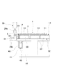
基板搬送手段14は、パネル基板1をステージ間間隔P毎にピッチ送りするものであって、その具体的な構成の一例を図6乃至図10に示す。基板搬送手段14は、図6に示したように、基板ピッチ送り駆動部30と、基板支持部31と、基板フローティング部32とから構成される。
The substrate transfer means 14 pitch-feeds the
基板ピッチ送り駆動部30は、可動ビーム40と、この可動ビーム40を昇降及び前後動させる駆動部材41とから構成される。可動ビーム40は、図7に示したように、表面に多数の吸着孔42を形成した方形のビームから構成され、内部には負圧配管43が接続されている。従って、可動ビーム40はパネル基板1を吸着保持できるようになっている。ここで、搬送される基板のサイズが同一か、または異なっていても、その差が僅かなものであれば、可動ビーム40の表面に設けられる吸着孔42は一定の箇所に設けておけば良い。しかしながら、異なるサイズの基板、また同じ基板でも処理する辺が短辺であるか、長辺であるかによっては、吸着孔の配置を異なるように設定しなければならない。このためには、図8に示したように、可動ビーム40に複数の負圧チャンバ44を設けておき、また可動ビーム40の表面に形成した複数の吸着孔42をこれら各負圧チャンバ44に接続するように構成する。そして、各負圧チャンバ44には、負圧配管43が接続されるが、これら各負圧配管43を電磁作動式の分配弁45に接続するようになし、必要な個所の分配弁45を開いて、パネル基板1が載置される個所の吸着孔42に負圧吸引力を作用させるようにする。また、パネル基板1を吸着する基板支持部材31についても、同様の構成を採用することができる。
The substrate pitch
駆動部材41はリニアモータステージ46上にスライダ47を設けたものであり、スライダ47はリニアモータにより駆動されて、ピッチ間隔P分を往復移動することになる。従って、基板ピッチ送り駆動部30は、この処理装置を構成するステージの数だけ設けられることになる。なお、駆動部材41は、リニアモータ方式ではなく、例えば送りねじ,シリンダ等により往復駆動するように構成することもできる。スライダ47上には昇降部材48が設けられており、この昇降部材48もリニアモータで駆動することもできる。昇降部材48の可動部48aは所定ストローク上下方向に往復移動することになる。なお、この昇降部材48はリニアモータではなく、シリンダやカム機構により駆動することもできる。可動ビーム40はこの昇降部材48の可動部48aに連結されている。
The
ここで、可動ビーム40の長さは、前述したピッチ間隔Pより短いものであり、しかも基板搬送手段14により搬送されるパネル基板1の最も長い辺の長さと同じかそれより長いものとしている。また、昇降部材48の可動部48aの昇降ストロークは、この可動部48aに連結した可動ビーム40の表面が、基板支持部31の表面より僅かに高い位置と、この基板支持部31の表面より低い位置との間である。また、基板支持部31は搬送経路のほぼ全長に及ぶ梁状の部材であって、基板ピッチ送り駆動部30を構成する可動ビーム40と同様、表面に多数の吸着孔を形成した方形ビームから構成される。
Here, the length of the
基板支持部31は各ステージ10〜13と平行に配設されており、パネル基板1に対しては、その処理対象となる縁部領域Eまたはこの縁部領域Eに近い位置において、パネル基板1の裏面を吸着して所定の位置に固定するために設けられている。ここで、各ステージ11〜13に設けたACF貼り付けユニット20,仮圧着ユニット21及び圧着ユニット22には、パネル基板1を支承する受け部20b,21b,22bが設けられているので、基板支持部31はこれらの受け部と干渉しない範囲でそれらにできるだけ近接した位置に設けられる。なお、基板支持部31を受け部として機能させることもできる。この場合には、基板支持部31はパネル基板1の縁部領域Eを含む位置に配置される。そして、基板ピッチ送り駆動部30を構成する可動ビーム40は、基板支持部31の前述した各処理ユニットの配設部とは反対側の部位に配置されており、しかも基板支持部31に近接した位置に設ける。
The
パネル基板1は、常に、基板支持部31または基板ピッチ送り駆動部30の可動ビーム40のいずれかに吸着保持されている。そして、これらの吸着部以外の部位はフローティングさせるようにしている。このために設けられているのが基板フローティング部32である。基板フローティング部32は、図9に示したように、加圧エアチャンバ50の上面にパンチングボード51を設けたものから構成され、加圧エアチャンバ50には加圧エアを供給するエア配管52が接続されている。パンチングボード51には多数の細孔51aが穿設されており、加圧エアチャンバ50からパンチングボード51の細孔51aから加圧エアを噴出させるようにしている。ここで、パンチングボード51から噴出する加圧エアは、このパネル基板1をパンチングボード51等とは非接触状態で搬送するためのものである。従って、パネル基板1の裏面との間に空気層を形成して、パネル基板1を浮上乃至フローティングさせた状態に保持するためのものであって、パネル基板1を押し上げるためのものではない。従って、ファンを用いて空気を加圧して、数kPa程度の圧力をパネル基板1の裏面に作用させれば、パンチングボード51とパネル基板1の裏面との間に空気層が形成されて、その間を非接触状態にすることができる。そして、基板フローティング部32は、最大のパネル基板の短辺側を処理しているときに、長辺の処理対象となる縁部領域とは反対側の縁部までの移動範囲の全体をカバーする構成としている。
The
以上のように構成することによって、パネル基板1の各辺に所定数のIC回路素子4を搭載することができる。ここで、フラットディスプレイパネルのサイズは様々あり、図10に示したように、小型サイズのパネル基板を1S,中型サイズのパネル基板を1M,大型サイズのパネル基板を1Lとしたときに、実線で示したように、その長辺側を処理対象とするにしても、仮想線で示したように、短辺側を処理対象とするにしても、各ステージ11〜13において、全て1つの角隅部を同じ位置に配置することができる。この角隅部の位置が基準位置Cとなる。即ち、ACF貼り付けステージ11におけるACF貼り付けユニット20やIC回路素子供給・仮圧着ステージ12における仮圧着ユニット21を基準位置Cから作動を開始するように制御する。
By configuring as described above, a predetermined number of
パネル基板1の搬送時の駆動は基板ピッチ送り駆動部30を構成する可動ビーム40であるから、前述したパネル基板1Sからパネル基板1Lまでの全てのサイズであって、しかもいずれの方向を向けたときにも、可動ビーム40と当接する。従って、必ず搬送駆動力をパネル基板1に作用させることができる。そして、パネル基板1の大半の部位は駆動力が作用しないが、可動ビーム40と当接する部位以外はパネル基板1の裏面側が基板フローティング部32と対面しており、この部位では、パンチングボード51から加圧エアが噴出して、この空気圧によりパネル基板1をフローティングすることになる。従って、基板ピッチ送り駆動部30の可動ビーム40によるパネル基板1の搬送時に、このパネル基板1が他の部材と摺接することはない。このために、可動ビーム40により軽い負荷でパネル基板1を搬送することができることになり、しかもパネル基板1を損傷させるようなことはない。
Since the driving at the time of transporting the
パネル基板1は、搬送時には前述した可動ビーム40に吸着させるが、各ステージにおいて処理を行っている間は基板支持部31に支持される。つまり、パネル基板1は可動ビーム40に吸着されている状態と基板支持部31に吸着されている状態とに切り換ることになる。従って、パネル基板1がステージ間を移行する際には、基板支持部31に吸着されているパネル基板1は、昇降部材48の作動により、可動ビーム40が真っ直ぐ上昇して、この可動ビーム40がパネル基板1と当接し、さらに可動ビーム40が上昇することによりパネル基板1は基板支持部31から剥離されて、可動ビーム40に吸着保持される状態となる。このときには、パネル基板1に対しては上方に変位する力が作用するが、横ずれしたり、回転方向にずれたりすることはない。ここで、可動ビーム40の上昇によるパネル基板1の位置は基板支持部31より僅かに高い位置とする。これによって、下方から弱い加圧エアが作用しているパネル基板1が変形するおそれはない。
The
パネル基板1が可動ビーム40に吸着される状態になると、可動ビーム40が前進することによって、前のステージから次のステージに向けて移動する。このときには、パネル基板1は処理対象となる縁部領域に近い部位のみが可動ビーム40に保持されているが、他の部位は基板フローティング部32によりフローティングした状態となっているので、パネル基板1の全体が円滑に次のステージに移行することになり、横ずれする方向や回転方向のモーメントが作用する等のおそれはない。
When the
パネル基板1が次のステージに移行すると、可動ビーム40が下降するが、真っ直ぐ下方に向けて下降する。このために、動作の途中でパネル基板1の裏面が基板支持部31に当接して、この基板支持部31により吸着保持されることになる。その結果、可動ビーム40の下降によりパネル基板1が剥離されるが、このときもパネル基板1に横ずれする方向や回転する方向へのずれが生じることはない。
When the
以上のことから、パネル基板1がステージ間を移行しても、その位置が実質的に位置ずれることがなく、常に一定の位置に保持される。ここで、基板搬送手段14はパネル基板1を厳格に位置決めする手段を有するものではないので、各ステージでは、ACF貼り付けユニット20,仮圧着ユニット21及び圧着ユニット22側で位置調整することになる。このときに、パネル基板1がほぼ一定の位置に配置されており、しかも各ステージでパネル基板1の処理対象とする縁部領域Eの搬送方向前方の角隅部が確実に基準位置Cに位置することから、これらの位置調整は簡単に、しかも円滑かつ迅速に行うことができる。このことは、パネル基板1のサイズが異なる場合であっても、またパネル基板1に対する処理対象とする縁部領域Eが長辺側であっても、短辺側であっても同様である。
From the above, even if the
1 パネル基板 2 下基板
3 上基板 4 IC回路素子
5 ACF 10 搬入部
11 ACF貼り付けステージ 12 IC回路素子供給・仮圧着ステージ
13 本圧着ステージ 20 ACF貼り付けユニット
21 仮圧着ユニット 22 圧着ユニット
30 基板ピッチ送り駆動部 31 基板支持部
32 基板フローティング部 40 可動ビーム
41 駆動部材 42 吸着孔
43 負圧配管 46 リニアモータステージ
47 スライダ 48 昇降部材
50 加圧エアチャンバ 51 パンチングボード
DESCRIPTION OF
Claims (6)
前記各処理機構の配列方向に沿って設けられ、前記基板を搬送する基板搬送手段は、
前記処理機構により前記基板に対して処理を行うときに、前記基板の被処理面とは反対側の裏面に負圧を作用させて前記基板を固定する基板支持部材と、
前記基板のうち処理対象となる縁部領域に近い部位のみを保持し、前記各処理機構の配列方向に向けて前記基板をピッチ送りする基板ピッチ送り駆動手段と、
前記各処理機構に対して前記基板ピッチ送り駆動手段を挟んだ反対側の部位に前記基板を浮上させる基板フロート手段と、
を備えていることを特徴とする基板処理装置。 A substrate processing apparatus for performing processing by each processing mechanism on an edge region of at least one side of the substrate while intermittently transporting the substrate constituting the display panel to a processing unit in which a plurality of processing mechanisms are arranged in a straight line In
Substrate transport means for transporting the substrate provided along the array direction of the processing mechanisms,
A substrate support member for fixing the substrate by applying a negative pressure to the back surface of the substrate opposite to the processing surface when processing the substrate by the processing mechanism;
A substrate pitch feed driving means for holding only the portion near the edge region to be processed among the substrates and pitch-feeding the substrates toward the arrangement direction of the processing mechanisms;
Substrate float means for levitating the substrate on the opposite side of the substrate pitch feed driving means with respect to each processing mechanism;
A substrate processing apparatus comprising:
前記基板の搬送を行うときには、前記可動ビームの表面に設けた複数の吸着部により前記基板の裏面に負圧を作用させ、前記基板に対して処理を行うときには、前記基板支持部材が前記基板の裏面に負圧を作用させるように切り替えを行うこと
を特徴とする請求項1記載の基板処理装置。 The substrate pitch feed driving means is of a walking beam type having a movable beam that operates in the order of ascending, advancing, descending, and retreating,
When transporting the substrate, negative pressure is applied to the back surface of the substrate by a plurality of suction portions provided on the surface of the movable beam, and when processing the substrate, the substrate support member is attached to the substrate. The substrate processing apparatus according to claim 1, wherein switching is performed so that a negative pressure is applied to the back surface.
前記吸着部に接続される複数の負圧チャンバと、
前記負圧チャンバに負圧を作用させる負圧配管に対して前記負圧チャンバごとに接続され、前記負圧チャンバに負圧を作用させるか否かを制御する分配弁と、
を備えていることを特徴とする請求項2記載の基板処理装置。 The movable beam has a length equal to or greater than the length of the longest side of the substrate to be transported;
A plurality of negative pressure chambers connected to the suction portion;
A distribution valve connected to each negative pressure chamber for a negative pressure pipe for applying a negative pressure to the negative pressure chamber, and controlling whether to apply a negative pressure to the negative pressure chamber;
The substrate processing apparatus according to claim 2, further comprising:
前記液晶パネル基板にACFを貼り付けるACFの貼り付け手段と、このACFを貼り付けた部位にIC回路素子を載置するためのIC回路素子供給・仮圧着手段と、前記IC回路素子を前記液晶パネル基板に熱圧着する圧着手段と、を備えたことを特徴とする請求項1乃至請求項5のうち何れか1項に記載の基板処理装置。 The substrate is a liquid crystal panel substrate, and the plurality of processing mechanisms are for mounting an IC circuit element on the liquid crystal panel substrate,
ACF adhering means for adhering ACF to the liquid crystal panel substrate, IC circuit element supply / temporary pressure bonding means for placing an IC circuit element on the ACF adhering portion, and the IC circuit element as the liquid crystal The substrate processing apparatus according to claim 1, further comprising a pressure-bonding unit that thermocompression-bonds to the panel substrate.
Priority Applications (1)
| Application Number | Priority Date | Filing Date | Title |
|---|---|---|---|
| JP2008195053A JP5373331B2 (en) | 2008-07-29 | 2008-07-29 | Substrate processing equipment |
Applications Claiming Priority (1)
| Application Number | Priority Date | Filing Date | Title |
|---|---|---|---|
| JP2008195053A JP5373331B2 (en) | 2008-07-29 | 2008-07-29 | Substrate processing equipment |
Publications (2)
| Publication Number | Publication Date |
|---|---|
| JP2010032786A JP2010032786A (en) | 2010-02-12 |
| JP5373331B2 true JP5373331B2 (en) | 2013-12-18 |
Family
ID=41737332
Family Applications (1)
| Application Number | Title | Priority Date | Filing Date |
|---|---|---|---|
| JP2008195053A Expired - Fee Related JP5373331B2 (en) | 2008-07-29 | 2008-07-29 | Substrate processing equipment |
Country Status (1)
| Country | Link |
|---|---|
| JP (1) | JP5373331B2 (en) |
Family Cites Families (3)
| Publication number | Priority date | Publication date | Assignee | Title |
|---|---|---|---|---|
| JP4378301B2 (en) * | 2005-02-28 | 2009-12-02 | 東京エレクトロン株式会社 | Substrate processing apparatus, substrate processing method, and substrate processing program |
| JP2006266722A (en) * | 2005-03-22 | 2006-10-05 | Olympus Corp | System and method for inspecting substrate |
| JP4854256B2 (en) * | 2005-10-06 | 2012-01-18 | 株式会社日立ハイテクノロジーズ | Panel processing apparatus and processing method |
-
2008
- 2008-07-29 JP JP2008195053A patent/JP5373331B2/en not_active Expired - Fee Related
Also Published As
| Publication number | Publication date |
|---|---|
| JP2010032786A (en) | 2010-02-12 |
Similar Documents
| Publication | Publication Date | Title |
|---|---|---|
| JP4729652B2 (en) | Component mounting apparatus and method | |
| TWI511225B (en) | Substrate transfer device and substrate assembly line | |
| JP4453849B2 (en) | ACF pasting method | |
| JP4489025B2 (en) | Crimping device | |
| JP2015199218A (en) | Workpiece attachment device | |
| US20030070280A1 (en) | Component mounting apparatus and component mounting method | |
| JP6675356B2 (en) | Electronic component mounting equipment | |
| KR100828312B1 (en) | Apparatus and Method for Bonding Printed Circuit on FPD Panel | |
| JP5373331B2 (en) | Substrate processing equipment | |
| KR20080020730A (en) | Apparatus and method for bonding printed circuit on fpd panel | |
| JP2017038012A (en) | Tray conveyance device and mounting device | |
| JP2010171088A (en) | Crimping device and crimping method | |
| JPWO2013141388A1 (en) | Electronic component mounting apparatus and mounting method | |
| KR20170070349A (en) | In-line Auto OLB/COG Common Bonding Apparatus | |
| JP4655187B2 (en) | TAB mounting apparatus and mounting method | |
| JP2009010123A (en) | Apparatus for mounting electronic component and method of manufacturing electronic component | |
| JP2009117704A (en) | Press bonding device, apparatus for manufacturing flat panel display and flat panel display | |
| JP6324860B2 (en) | Semiconductor or electronic component mounting apparatus and semiconductor or electronic component mounting method | |
| KR101042536B1 (en) | Unit for separating a ACF layer from a ACF tape and apparatus for bonding a ACF having the unit | |
| JP2012123134A (en) | Fpd module assembly device | |
| WO2022244804A1 (en) | Substrate processing apparatus and substrate processing method | |
| JP2011097095A (en) | Pressure bonding apparatus and method for manufacturing flat panel display | |
| JP2011077440A (en) | Substrate transfer apparatus and liquid crystal cell | |
| JP2012203304A (en) | Fpd module assembling device | |
| JP4607815B2 (en) | Joining sheet affixing device and method |
Legal Events
| Date | Code | Title | Description |
|---|---|---|---|
| A621 | Written request for application examination |
Free format text: JAPANESE INTERMEDIATE CODE: A621 Effective date: 20100802 |
|
| A131 | Notification of reasons for refusal |
Free format text: JAPANESE INTERMEDIATE CODE: A131 Effective date: 20120228 |
|
| A977 | Report on retrieval |
Free format text: JAPANESE INTERMEDIATE CODE: A971007 Effective date: 20120229 |
|
| A521 | Written amendment |
Free format text: JAPANESE INTERMEDIATE CODE: A523 Effective date: 20120426 |
|
| A131 | Notification of reasons for refusal |
Free format text: JAPANESE INTERMEDIATE CODE: A131 Effective date: 20121030 |
|
| A521 | Written amendment |
Free format text: JAPANESE INTERMEDIATE CODE: A523 Effective date: 20121226 |
|
| RD04 | Notification of resignation of power of attorney |
Free format text: JAPANESE INTERMEDIATE CODE: A7424 Effective date: 20130329 |
|
| RD02 | Notification of acceptance of power of attorney |
Free format text: JAPANESE INTERMEDIATE CODE: A7422 Effective date: 20130409 |
|
| TRDD | Decision of grant or rejection written | ||
| A01 | Written decision to grant a patent or to grant a registration (utility model) |
Free format text: JAPANESE INTERMEDIATE CODE: A01 Effective date: 20130910 |
|
| A61 | First payment of annual fees (during grant procedure) |
Free format text: JAPANESE INTERMEDIATE CODE: A61 Effective date: 20130919 |
|
| R150 | Certificate of patent or registration of utility model |
Free format text: JAPANESE INTERMEDIATE CODE: R150 |
|
| LAPS | Cancellation because of no payment of annual fees |