JP5367576B2 - 材料製造方法 - Google Patents
材料製造方法 Download PDFInfo
- Publication number
- JP5367576B2 JP5367576B2 JP2009531308A JP2009531308A JP5367576B2 JP 5367576 B2 JP5367576 B2 JP 5367576B2 JP 2009531308 A JP2009531308 A JP 2009531308A JP 2009531308 A JP2009531308 A JP 2009531308A JP 5367576 B2 JP5367576 B2 JP 5367576B2
- Authority
- JP
- Japan
- Prior art keywords
- oxygen
- light
- singlet oxygen
- singlet
- wavelength
- Prior art date
- Legal status (The legal status is an assumption and is not a legal conclusion. Google has not performed a legal analysis and makes no representation as to the accuracy of the status listed.)
- Active
Links
Images


Classifications
-
- G—PHYSICS
- G02—OPTICS
- G02B—OPTICAL ELEMENTS, SYSTEMS OR APPARATUS
- G02B6/00—Light guides; Structural details of arrangements comprising light guides and other optical elements, e.g. couplings
- G02B6/24—Coupling light guides
- G02B6/42—Coupling light guides with opto-electronic elements
- G02B6/4201—Packages, e.g. shape, construction, internal or external details
- G02B6/4204—Packages, e.g. shape, construction, internal or external details the coupling comprising intermediate optical elements, e.g. lenses, holograms
- G02B6/4212—Packages, e.g. shape, construction, internal or external details the coupling comprising intermediate optical elements, e.g. lenses, holograms the intermediate optical element being a coupling medium interposed therebetween, e.g. epoxy resin, refractive index matching material, index grease, matching liquid or gel
-
- C—CHEMISTRY; METALLURGY
- C08—ORGANIC MACROMOLECULAR COMPOUNDS; THEIR PREPARATION OR CHEMICAL WORKING-UP; COMPOSITIONS BASED THEREON
- C08J—WORKING-UP; GENERAL PROCESSES OF COMPOUNDING; AFTER-TREATMENT NOT COVERED BY SUBCLASSES C08B, C08C, C08F, C08G or C08H
- C08J7/00—Chemical treatment or coating of shaped articles made of macromolecular substances
- C08J7/12—Chemical modification
- C08J7/16—Chemical modification with polymerisable compounds
- C08J7/18—Chemical modification with polymerisable compounds using wave energy or particle radiation
-
- G—PHYSICS
- G02—OPTICS
- G02B—OPTICAL ELEMENTS, SYSTEMS OR APPARATUS
- G02B6/00—Light guides; Structural details of arrangements comprising light guides and other optical elements, e.g. couplings
- G02B6/10—Light guides; Structural details of arrangements comprising light guides and other optical elements, e.g. couplings of the optical waveguide type
- G02B6/12—Light guides; Structural details of arrangements comprising light guides and other optical elements, e.g. couplings of the optical waveguide type of the integrated circuit kind
- G02B6/122—Basic optical elements, e.g. light-guiding paths
- G02B6/1221—Basic optical elements, e.g. light-guiding paths made from organic materials
-
- G—PHYSICS
- G02—OPTICS
- G02B—OPTICAL ELEMENTS, SYSTEMS OR APPARATUS
- G02B6/00—Light guides; Structural details of arrangements comprising light guides and other optical elements, e.g. couplings
- G02B6/10—Light guides; Structural details of arrangements comprising light guides and other optical elements, e.g. couplings of the optical waveguide type
- G02B6/12—Light guides; Structural details of arrangements comprising light guides and other optical elements, e.g. couplings of the optical waveguide type of the integrated circuit kind
- G02B2006/12166—Manufacturing methods
- G02B2006/1219—Polymerisation
Landscapes
- Physics & Mathematics (AREA)
- Chemical & Material Sciences (AREA)
- General Physics & Mathematics (AREA)
- Optics & Photonics (AREA)
- Health & Medical Sciences (AREA)
- General Chemical & Material Sciences (AREA)
- Toxicology (AREA)
- Chemical Kinetics & Catalysis (AREA)
- Medicinal Chemistry (AREA)
- Polymers & Plastics (AREA)
- Organic Chemistry (AREA)
- Engineering & Computer Science (AREA)
- Microelectronics & Electronic Packaging (AREA)
- Treatments Of Macromolecular Shaped Articles (AREA)
- Semiconductor Lasers (AREA)
Description
2,21,22 レーザダイオード
3 ファイバ
4 出射管
5,205 制御部
6 入力部
7 出力部
10 処理対象物
215 酸素供給機構
216 酸素供給管
301 光モジュール
302 本体部
303 フェルール部
310 半導体レーザ
320 透明樹脂
330 光ファイバ
3120 第1部分(透明樹脂の変質部)
3130 第2部分(透明樹脂の未変質部)
3200 光導波路
400 光ファイバ接続構造
401、402 コネクタフェルール
4011〜4014、4021〜4024 光ファイバ
403 導波路フィルム
4031〜4034 変質部
4035 未変質部
404 フィルム基材
500 光光路変換構造
501 光ファイバ
502 プリズム
503 受光素子
504 導波路部材
5041、5042 変質部
5043 未変質部
505 基材

つぎに、本発明の他の実施形態について説明する。図19は、本発明の他の実施形態1に係る光ファイバ接続構造の模式的な断面図である。この光ファイバ接続構造400は、コネクタフェルール401と、コネクタフェルール402とが、導波路フィルム403を介在させて突き合わせた状態で接続した構造を有している。コネクタフェルール401、402には、それぞれアレイ状に並べた4本の光ファイバ4011〜4014、4021〜4024が挿通固定されている。また、コネクタフェルール401、402は、不図示のラッチ構造またはクリップ等で互いに固定されている。ここで、導波路フィルム403には、たとえば酸化シリコンからなる変質部4031〜4034と、変質部4031〜4034よりも屈折率が低い、たとえばシリコーン樹脂からなる未変質部4035とが構成する光導波路が形成されている。そして、対向して配置された光ファイバ4011と光ファイバ4021は、変質部4031と未変質部4035とが構成する光導波路によって光学的に接続している。また、他の対向する光ファイバ同士もそれぞれ対応する光導波路によって光学的に接続している。なお、変質部4031〜4034の屈折率は1.46に近く、光ファイバ4011〜4014、4021〜4024と屈折率の整合がとれているため、変質部と光ファイバとの界面での反射はきわめて低く抑制されている。
つぎに、本発明のさらに他の実施形態について説明する。図21は、本発明の他の実施形態2に係る光経路変換構造の模式的な断面図である。この光経路変換構造500は、光ファイバ501と、反射手段としての反射面の反射率を金蒸着等により高めた三角プリズム等のプリズム502と、フォトダイオード等の受光素子503と、導波路部材504とを備える。ここで、導波路部材504は、たとえば酸化シリコンからなる変質部5041、5042と、変質部5041、5042よりも屈折率が低い、たとえばシリコーン樹脂からなる未変質部5043から構成される光導波路が形成されている。変質部5041は、光ファイバ501から出射した光L51をプリズム502へ導波するように配置されている。また、プリズム502は、その反射面5021で光L51を反射し、光L51の伝搬方向を90度だけ回転するように配置されている。また、変質部5042は、表面5021で反射した光L51を受光素子503へ導波するように配置されている。すなわち、この光経路変換構造500は、光ファイバ501から出射した光L51の光路を90度だけ回転するような機能を有するものである。なお、光L51の波長は特に限定されないが、たとえば光ファイバ通信で最も用いられる波長1310nm近傍、あるいは1550nm近傍の光とすることができる。
Claims (9)
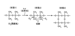
- シリコーン樹脂である材料の内部に酸素分子を透過させた状態、または該材料表面に酸素分子を存在させた状態で少なくとも酸素分子を一重項酸素化できるエネルギーを有した光を照射し一重項酸素を発生させ、該発生させた一重項酸素で前記材料中の分子構造の結合を切断することによって重合化反応または置換反応を行わせて、前記材料の分子量を変化させて所望の材料を製造することを特徴とする材料製造方法。
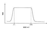
- 少なくとも1270nm近傍の波長を含む光を照射して前記一重項酸素を発生させることを特徴とする請求項1に記載の材料製造方法。
- 前記所望の材料は、前記材料よりも分子量が大きいことを特徴とする請求項1または2に記載の材料製造方法。
- 前記所望の材料は、前記材料よりも分子量が小さいことを特徴とする請求項1または2に記載の材料製造方法。
- 当該材料製造方法は、前記発生させた一重項酸素で前記シリコーン樹脂中のメチル基を切断することによって重合化反応または置換反応を行わせてガラス化することを特徴とする請求項1〜4のいずれか一つに記載の材料製造方法。
- 前記少なくとも酸素分子を一重項酸素化できるエネルギーを有した光とともに前記メチル基以外の基を切断できるエネルギーを有した光を照射することによって、前記メチル基以外の基を切断し、生成した一重項酸素を用いて前記メチル基以外の基を切断した位置で重合化反応または置換反応を行なわせることを特徴とする請求項5に記載の材料製造方法。
- 1270nm近傍にピークを有する光を照射して前記一重項酸素を発生させることを特徴とする請求項2〜6のいずれか一つに記載の材料製造方法。
- 少なくとも1270nm近傍の波長を含むレーザ光を照射して前記一重項酸素を発生させることを特徴とする請求項2〜7のいずれか一つに記載の材料製造方法。
- 前記材料を酸素雰囲気中に設置した状態で前記少なくとも酸素分子を一重項酸素化できるエネルギーを有した光を照射して前記一重項酸素を発生させることを特徴とする請求項1〜8のいずれか一つに記載の材料製造方法。
Priority Applications (1)
| Application Number | Priority Date | Filing Date | Title |
|---|---|---|---|
| JP2009531308A JP5367576B2 (ja) | 2007-09-07 | 2008-09-08 | 材料製造方法 |
Applications Claiming Priority (6)
| Application Number | Priority Date | Filing Date | Title |
|---|---|---|---|
| JP2007233348 | 2007-09-07 | ||
| JP2007233348 | 2007-09-07 | ||
| JP2008092346 | 2008-03-31 | ||
| JP2008092346 | 2008-03-31 | ||
| PCT/JP2008/066194 WO2009031685A1 (ja) | 2007-09-07 | 2008-09-08 | 材料製造方法 |
| JP2009531308A JP5367576B2 (ja) | 2007-09-07 | 2008-09-08 | 材料製造方法 |
Publications (2)
| Publication Number | Publication Date |
|---|---|
| JPWO2009031685A1 JPWO2009031685A1 (ja) | 2010-12-16 |
| JP5367576B2 true JP5367576B2 (ja) | 2013-12-11 |
Family
ID=40428996
Family Applications (1)
| Application Number | Title | Priority Date | Filing Date |
|---|---|---|---|
| JP2009531308A Active JP5367576B2 (ja) | 2007-09-07 | 2008-09-08 | 材料製造方法 |
Country Status (5)
| Country | Link |
|---|---|
| US (1) | US20100160479A1 (ja) |
| EP (1) | EP2186851A1 (ja) |
| JP (1) | JP5367576B2 (ja) |
| CN (1) | CN101796107B (ja) |
| WO (1) | WO2009031685A1 (ja) |
Families Citing this family (1)
| Publication number | Priority date | Publication date | Assignee | Title |
|---|---|---|---|---|
| US10338325B1 (en) * | 2018-06-01 | 2019-07-02 | International Business Machines Corporation | Nanofiller in an optical interface |
Citations (5)
| Publication number | Priority date | Publication date | Assignee | Title |
|---|---|---|---|---|
| JPH03128941A (ja) * | 1989-10-14 | 1991-05-31 | I S I:Kk | 素材の表面改質方法 |
| JPH03128947A (ja) * | 1989-10-14 | 1991-05-31 | I S I:Kk | 素材の表面改質方法 |
| JPH0559177A (ja) * | 1987-11-12 | 1993-03-09 | Dow Corning Corp | 紫外線処理によるプレセラミツクポリマーの不溶融化方法 |
| JPH11236460A (ja) * | 1998-02-20 | 1999-08-31 | Dainippon Printing Co Ltd | プラスチックフィルムの表面処理方法 |
| JP2001110802A (ja) * | 1999-10-06 | 2001-04-20 | Matsushita Electric Ind Co Ltd | 絶縁膜の形成方法 |
Family Cites Families (3)
| Publication number | Priority date | Publication date | Assignee | Title |
|---|---|---|---|---|
| IT998906B (it) * | 1973-10-24 | 1976-02-20 | Snam Progetti | Procedimento per bendere degrada bili i polimeri |
| US7404990B2 (en) * | 2002-11-14 | 2008-07-29 | Air Products And Chemicals, Inc. | Non-thermal process for forming porous low dielectric constant films |
| US20080020941A1 (en) * | 2005-03-24 | 2008-01-24 | Jimpei Tabata | Biomolecule-immobilized plate and method for fabricating biomolecule-immobilized plate |
-
2008
- 2008-09-08 JP JP2009531308A patent/JP5367576B2/ja active Active
- 2008-09-08 EP EP08828984A patent/EP2186851A1/en not_active Withdrawn
- 2008-09-08 CN CN2008801058229A patent/CN101796107B/zh not_active Expired - Fee Related
- 2008-09-08 WO PCT/JP2008/066194 patent/WO2009031685A1/ja not_active Ceased
-
2010
- 2010-03-05 US US12/718,577 patent/US20100160479A1/en not_active Abandoned
Patent Citations (5)
| Publication number | Priority date | Publication date | Assignee | Title |
|---|---|---|---|---|
| JPH0559177A (ja) * | 1987-11-12 | 1993-03-09 | Dow Corning Corp | 紫外線処理によるプレセラミツクポリマーの不溶融化方法 |
| JPH03128941A (ja) * | 1989-10-14 | 1991-05-31 | I S I:Kk | 素材の表面改質方法 |
| JPH03128947A (ja) * | 1989-10-14 | 1991-05-31 | I S I:Kk | 素材の表面改質方法 |
| JPH11236460A (ja) * | 1998-02-20 | 1999-08-31 | Dainippon Printing Co Ltd | プラスチックフィルムの表面処理方法 |
| JP2001110802A (ja) * | 1999-10-06 | 2001-04-20 | Matsushita Electric Ind Co Ltd | 絶縁膜の形成方法 |
Also Published As
| Publication number | Publication date |
|---|---|
| EP2186851A1 (en) | 2010-05-19 |
| CN101796107B (zh) | 2012-08-22 |
| WO2009031685A1 (ja) | 2009-03-12 |
| CN101796107A (zh) | 2010-08-04 |
| US20100160479A1 (en) | 2010-06-24 |
| JPWO2009031685A1 (ja) | 2010-12-16 |
Similar Documents
| Publication | Publication Date | Title |
|---|---|---|
| WO2010095333A1 (ja) | 近接場光発生器、光記録ヘッド及び光記録装置 | |
| US20170123147A1 (en) | Robust Fiber Cell for Atomic and Molecular Sensing | |
| US20020001320A1 (en) | Laser device and light signal amplifying device using the same | |
| JP4564502B2 (ja) | 光ビームの出力カプラを提供する方法および装置 | |
| JP5367576B2 (ja) | 材料製造方法 | |
| WO2006075760A1 (ja) | 変調機能付光源装置とその駆動方法 | |
| CN113365775B (zh) | 构造体、构造体的制造方法、激光装置及激光系统 | |
| JP7124632B2 (ja) | 光接続構造およびその形成方法 | |
| Namekawa et al. | Simultaneous multi-core fiber-to-fiber self-coupling with near-infrared light-induced self-written optical waveguide | |
| US20100027569A1 (en) | Uv diode-laser module with optical fiber delivery | |
| US9395502B2 (en) | Apparatus and method for coupling optical signals between optical fibers and photo devices | |
| WO2022102053A1 (ja) | 光接続構造、光モジュールおよび光接続構造の製造方法 | |
| JP2005215426A (ja) | 半導体レーザモジュール | |
| KR102408995B1 (ko) | 분산된 그래핀을 수용한 폴리머 도파로 및 이를 제조하는 방법, 그리고 이 폴리머 도파로 기반의 수동 모드 잠금 레이저 | |
| JP2009080142A (ja) | 光モジュール | |
| JP7758039B2 (ja) | 光回路デバイス | |
| JP2004334003A (ja) | 光結合素子の製造法及び光記録装置 | |
| JP2009192678A (ja) | 光導波路及び光装置 | |
| US20040165839A1 (en) | Method and device for coupling a light emitting source to an optical waveguide | |
| JP2004004396A (ja) | 光導波路用材料、光導波路及びその製造方法 | |
| WO2024121894A1 (ja) | 光素子および光素子の製造方法 | |
| JP4710046B2 (ja) | 光記録装置 | |
| WO2024252770A1 (ja) | 光伝送路及びその製造方法 | |
| JP2025024828A (ja) | 光デバイス、及び光トランシーバ | |
| JP5158869B2 (ja) | 光モジュール |
Legal Events
| Date | Code | Title | Description |
|---|---|---|---|
| A621 | Written request for application examination |
Free format text: JAPANESE INTERMEDIATE CODE: A621 Effective date: 20110601 |
|
| A131 | Notification of reasons for refusal |
Free format text: JAPANESE INTERMEDIATE CODE: A131 Effective date: 20130604 |
|
| A521 | Request for written amendment filed |
Free format text: JAPANESE INTERMEDIATE CODE: A523 Effective date: 20130801 |
|
| TRDD | Decision of grant or rejection written | ||
| A01 | Written decision to grant a patent or to grant a registration (utility model) |
Free format text: JAPANESE INTERMEDIATE CODE: A01 Effective date: 20130827 |
|
| A61 | First payment of annual fees (during grant procedure) |
Free format text: JAPANESE INTERMEDIATE CODE: A61 Effective date: 20130911 |
|
| R151 | Written notification of patent or utility model registration |
Ref document number: 5367576 Country of ref document: JP Free format text: JAPANESE INTERMEDIATE CODE: R151 |
|
| S531 | Written request for registration of change of domicile |
Free format text: JAPANESE INTERMEDIATE CODE: R313531 |
|
| R350 | Written notification of registration of transfer |
Free format text: JAPANESE INTERMEDIATE CODE: R350 |