JP5367576B2 - Material manufacturing method - Google Patents
Material manufacturing method Download PDFInfo
- Publication number
- JP5367576B2 JP5367576B2 JP2009531308A JP2009531308A JP5367576B2 JP 5367576 B2 JP5367576 B2 JP 5367576B2 JP 2009531308 A JP2009531308 A JP 2009531308A JP 2009531308 A JP2009531308 A JP 2009531308A JP 5367576 B2 JP5367576 B2 JP 5367576B2
- Authority
- JP
- Japan
- Prior art keywords
- oxygen
- light
- singlet oxygen
- singlet
- wavelength
- Prior art date
- Legal status (The legal status is an assumption and is not a legal conclusion. Google has not performed a legal analysis and makes no representation as to the accuracy of the status listed.)
- Active
Links
Images


Classifications
-
- G—PHYSICS
- G02—OPTICS
- G02B—OPTICAL ELEMENTS, SYSTEMS OR APPARATUS
- G02B6/00—Light guides; Structural details of arrangements comprising light guides and other optical elements, e.g. couplings
- G02B6/24—Coupling light guides
- G02B6/42—Coupling light guides with opto-electronic elements
- G02B6/4201—Packages, e.g. shape, construction, internal or external details
- G02B6/4204—Packages, e.g. shape, construction, internal or external details the coupling comprising intermediate optical elements, e.g. lenses, holograms
- G02B6/4212—Packages, e.g. shape, construction, internal or external details the coupling comprising intermediate optical elements, e.g. lenses, holograms the intermediate optical element being a coupling medium interposed therebetween, e.g. epoxy resin, refractive index matching material, index grease, matching liquid or gel
-
- C—CHEMISTRY; METALLURGY
- C08—ORGANIC MACROMOLECULAR COMPOUNDS; THEIR PREPARATION OR CHEMICAL WORKING-UP; COMPOSITIONS BASED THEREON
- C08J—WORKING-UP; GENERAL PROCESSES OF COMPOUNDING; AFTER-TREATMENT NOT COVERED BY SUBCLASSES C08B, C08C, C08F, C08G or C08H
- C08J7/00—Chemical treatment or coating of shaped articles made of macromolecular substances
- C08J7/12—Chemical modification
- C08J7/16—Chemical modification with polymerisable compounds
- C08J7/18—Chemical modification with polymerisable compounds using wave energy or particle radiation
-
- G—PHYSICS
- G02—OPTICS
- G02B—OPTICAL ELEMENTS, SYSTEMS OR APPARATUS
- G02B6/00—Light guides; Structural details of arrangements comprising light guides and other optical elements, e.g. couplings
- G02B6/10—Light guides; Structural details of arrangements comprising light guides and other optical elements, e.g. couplings of the optical waveguide type
- G02B6/12—Light guides; Structural details of arrangements comprising light guides and other optical elements, e.g. couplings of the optical waveguide type of the integrated circuit kind
- G02B6/122—Basic optical elements, e.g. light-guiding paths
- G02B6/1221—Basic optical elements, e.g. light-guiding paths made from organic materials
-
- G—PHYSICS
- G02—OPTICS
- G02B—OPTICAL ELEMENTS, SYSTEMS OR APPARATUS
- G02B6/00—Light guides; Structural details of arrangements comprising light guides and other optical elements, e.g. couplings
- G02B6/10—Light guides; Structural details of arrangements comprising light guides and other optical elements, e.g. couplings of the optical waveguide type
- G02B6/12—Light guides; Structural details of arrangements comprising light guides and other optical elements, e.g. couplings of the optical waveguide type of the integrated circuit kind
- G02B2006/12166—Manufacturing methods
- G02B2006/1219—Polymerisation
Abstract
Description
この発明は、重合化反応または置換反応を行わせて材料の分子量を変化させて所望の材料を製造する材料製造方法に関する。 The present invention relates to a material manufacturing method for manufacturing a desired material by changing a molecular weight of a material by performing a polymerization reaction or a substitution reaction.
従来から、熱処理によって、通常の酸素分子(O2)よりも活性化された状態の活性化酸素を発生させ、この活性化酸素を用いて材料の特性を変化させる方法が知られている(非特許文献1参照)。このような活性化酸素として、スーパーオキシド(・O2 −)、ヒドロキシルラジカル(HO・)、一重項酸素(1O2)がある。Conventionally, there has been known a method of generating activated oxygen in a state of being activated more than normal oxygen molecules (O 2 ) by heat treatment, and changing the characteristics of the material using the activated oxygen (non-native). Patent Document 1). Such activation oxygen, superoxide (· O 2 -), hydroxyl radical (HO ·), there is a singlet oxygen (1 O 2).
しかしながら、従来の熱処理による方法では、特性変化処理対象の材料に熱を加えることによって、特性変化処理対象以外の他の領域や他の材料も熱せられてしまい、これらの他の部分も変質してしまうため、特性変化処理対象以外の他の領域や他の材料の特性の維持が難しかった。すなわち、従来の熱処理による方法では、活性化酸素を用いて局所的に材料の特性を変化させて所望の材料を製造することは困難であった。 However, in the conventional heat treatment method, by applying heat to the material subject to property change processing, other regions other than the property change subject and other materials are also heated, and these other parts are also altered. For this reason, it is difficult to maintain the characteristics of other regions and other materials than the property change processing target. That is, in the conventional heat treatment method, it is difficult to produce a desired material by locally changing the characteristics of the material using activated oxygen.
本発明は、活性化酸素を用いて材料の特性を局所的に変化できる材料製造方法を提供することを目的とする。 An object of this invention is to provide the material manufacturing method which can change the characteristic of a material locally using activated oxygen.
上述した課題を解決し、目的を達成するために、この発明にかかる材料製造方法は、材料内部に酸素分子を透過させた状態、または該材料表面に酸素分子を存在させた状態で少なくとも酸素分子を一重項酸素化できるエネルギーを有した光を照射し一重項酸素を発生させ、該発生させた一重項酸素で前記材料中の分子構造の結合を切断することによって重合化反応または置換反応を行わせて、前記材料の分子量を変化させて所望の材料を製造することを特徴とする。 In order to solve the above-described problems and achieve the object, the material manufacturing method according to the present invention is a method in which at least oxygen molecules are transmitted in a state where oxygen molecules are permeated inside the material or in a state where oxygen molecules are present on the material surface. A polymerization reaction or a substitution reaction is performed by irradiating light having energy capable of singlet oxygenation to generate singlet oxygen, and breaking the molecular structure bond in the material with the generated singlet oxygen. Accordingly, a desired material is manufactured by changing the molecular weight of the material.
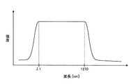
また、この発明にかかる材料製造方法は、上記発明において、少なくとも1270nm近傍の波長を含む光を照射して前記一重項酸素を発生させることを特徴とする。 The material manufacturing method according to the present invention is characterized in that, in the above invention, the singlet oxygen is generated by irradiating light having a wavelength of at least about 1270 nm.
また、この発明にかかる材料製造方法は、上記発明において、前記所望の材料は、前記材料よりも分子量が大きいことを特徴とする。 In the material manufacturing method according to the present invention as set forth in the invention described above, the desired material has a molecular weight larger than that of the material.
また、この発明にかかる材料製造方法は、上記発明において、前記所望の材料は、前記材料よりも分子量が小さいことを特徴とする。 In the material manufacturing method according to the present invention as set forth in the invention described above, the desired material has a molecular weight smaller than that of the material.
また、この発明にかかる材料製造方法は、上記発明において、前記材料は、シリコーン樹脂であることを特徴とする。 In the material manufacturing method according to the present invention as set forth in the invention described above, the material is a silicone resin.
また、この発明にかかる材料製造方法は、上記発明において、当該材料製造方法は、前記発生させた一重項酸素で前記シリコーン樹脂中のメチル基を切断することによって重合化反応または置換反応を行わせてガラス化することを特徴とする。 Further, the material manufacturing method according to the present invention is the above invention, wherein the material manufacturing method performs a polymerization reaction or a substitution reaction by cleaving a methyl group in the silicone resin with the generated singlet oxygen. It is characterized by vitrification.
また、この発明にかかる材料製造方法は、上記発明において、前記少なくとも酸素分子を一重項酸素化できるエネルギーを有した光とともに前記メチル基以外の基を切断できるエネルギーを有した光を照射することによって、前記メチル基以外の基を切断し、生成した一重項酸素を用いて前記メチル基以外の基を切断した位置で重合化反応または置換反応を行なわせることを特徴とする。 Moreover, in the material manufacturing method according to the present invention, in the above invention, by irradiating light having energy capable of cleaving a group other than the methyl group together with light having energy capable of singlet oxygenation of at least oxygen molecules. The method is characterized in that a group other than the methyl group is cleaved, and a polymerization reaction or a substitution reaction is performed at a position where the group other than the methyl group is cleaved using the generated singlet oxygen.
また、この発明にかかる材料製造方法は、上記発明において、1270nm近傍にピークを有する光を照射して前記一重項酸素を発生させることを特徴とする。 The material manufacturing method according to the present invention is characterized in that, in the above-mentioned invention, the singlet oxygen is generated by irradiating light having a peak near 1270 nm.
また、この発明にかかる材料製造方法は、上記発明において、少なくとも1270nm近傍の波長を含むレーザ光を照射して前記一重項酸素を発生させることを特徴とする。 The material manufacturing method according to the present invention is characterized in that, in the above-mentioned invention, the singlet oxygen is generated by irradiating a laser beam having a wavelength of at least about 1270 nm.
また、この発明にかかる材料製造方法は、上記発明において、前記材料を酸素雰囲気中に設置した状態で前記少なくとも酸素分子を一重項酸素化できるエネルギーを有した光を照射して前記一重項酸素を発生させることを特徴とする。 Further, in the material manufacturing method according to the present invention, in the above invention, the singlet oxygen is irradiated by irradiating light having energy capable of singlet oxygenation of the at least oxygen molecules in a state where the material is placed in an oxygen atmosphere. It is characterized by generating.
本発明によれば、材料に酸素分子を透過させた状態で少なくとも酸素分子を一重項酸素化できるエネルギーを有した光を処理対照部分に照射し一重項酸素を発生させ、該発生させた一重項酸素で材料中の分子構造の結合を切断することによって重合化反応または置換反応を行わせて、材料の分子量を変化させて所望の材料を製造するため、熱処理を行なわなくとも活性化酸素を用いて材料の特性を局所的に変化することが可能になる。 According to the present invention, the singlet oxygen is generated by irradiating the treatment control portion with light having energy capable of at least oxygen molecule oxygenation in the state where the oxygen molecule is transmitted through the material, and generating the singlet oxygen. In order to produce a desired material by changing the molecular weight of the material by breaking the molecular structure bond in the material with oxygen to change the molecular weight of the material, activated oxygen is used without heat treatment. This makes it possible to locally change the properties of the material.
1,201 製造装置
2,21,22 レーザダイオード
3 ファイバ
4 出射管
5,205 制御部
6 入力部
7 出力部
10 処理対象物
215 酸素供給機構
216 酸素供給管
301 光モジュール
302 本体部
303 フェルール部
310 半導体レーザ
320 透明樹脂
330 光ファイバ
3120 第1部分(透明樹脂の変質部)
3130 第2部分(透明樹脂の未変質部)
3200 光導波路
400 光ファイバ接続構造
401、402 コネクタフェルール
4011〜4014、4021〜4024 光ファイバ
403 導波路フィルム
4031〜4034 変質部
4035 未変質部
404 フィルム基材
500 光光路変換構造
501 光ファイバ
502 プリズム
503 受光素子
504 導波路部材
5041、5042 変質部
5043 未変質部
505 基材DESCRIPTION OF SYMBOLS 1,201
3130 2nd part (unmodified part of transparent resin)
3200
以下、図面を参照して、この発明の実施の形態について、図面に基づいて説明する。なお、この実施の形態によりこの発明が限定されるものではない。図面の記載において、同一部分には同一の符号を付している。 Embodiments of the present invention will be described below with reference to the drawings. Note that the present invention is not limited to the embodiments. In the description of the drawings, the same parts are denoted by the same reference numerals.
図1は、本実施の形態における製造装置の要部構成を示す図である。図1に示すように、本実施の形態における製造装置1は、所定帯域の波長のレーザ光を発するレーザダイオード2、レーザダイオード2が発したレーザ光を伝送するファイバ3、ファイバ3から伝送されたレーザ光の出射口を有する出射管4、製造装置1の各構成部位を制御する制御部5、製造装置1の処理動作に要する諸情報や製造処理に対する指示情報等を外部から取得する入力部6、および、処理結果などの諸情報を出力する出力部7を備える。制御部5は、レーザダイオード2のレーザ光の出射や出力を制御する。
FIG. 1 is a diagram showing a main configuration of the manufacturing apparatus according to the present embodiment. As shown in FIG. 1, the
レーザダイオード2は、1270nmをピークとするレーザ光Lを発し、レーザダイオード2が発したレーザ光は、ファイバ3および出射管4を介して、処理対象物10内部の処理対象領域Aに照射される。
The
処理対象物10は、酸素分子(O2)11が内部に透過可能である材料である。言い換えると、処理対象物10は、金属板のように内部に気体が浸入できないものではなく、少なくとも処理対象領域Aまで気体状の酸素分子が透過できる程度のスペースを骨格間に有するものであり、たとえば大気中に設置された場合には、材料内部に気体状の酸素分子が透過できるものである。The
ここで、酸素分子は、所定のエネルギーを吸収することによって、基底状態(三重項酸素:3Σ−(0))から励起状態の一重項酸素になる。具体的には、図2に示すように、酸素分子が、基底状態から、反結合性の軌道の不対電子1個がスピンの向きを変えた1Σg +(0)の一重項酸素になるためには、1.63eVのエネルギーが必要となる。たとえば、1.63eVに対応する762nmの波長の光が酸素分子に照射されることによって、酸素分子が励起され、1Σg +(0)の一重項酸素が生成する。Here, oxygen molecules change from ground state (triplet oxygen: 3 Σ − (0)) to singlet oxygen in an excited state by absorbing predetermined energy. Specifically, as shown in FIG. 2, the oxygen molecule changes from the ground state to a singlet oxygen of 1 Σ g + (0) in which one unpaired electron in the antibonding orbit changes the direction of the spin. In order to achieve this, an energy of 1.63 eV is required. For example, when oxygen molecules are irradiated with light having a wavelength of 762 nm corresponding to 1.63 eV, the oxygen molecules are excited to generate singlet oxygen of 1 Σ g + (0).
また、酸素分子が、基底状態から、反結合性の軌道の不対電子が別の軌道に入って該別の軌道に存在した異なるスピンの不対電子と対になって互いのスピンを打ち消すようになった1Δg(0)の一重項酸素になるためには、0.98eVのエネルギーが必要となる。たとえば、0.98eVに対応する1270nm近傍の波長の光が酸素分子に照射されることによって、酸素分子が励起され、1Δg(0)の一重項酸素が生成する。そして、以下の化学反応式(a)に示すように、酸素分子(O2)に1270nmの波長の光を照射することによって、1Δg(0)の一重項酸素(1O2)が生成する。
![]()
![]()
この一重項酸素は、通常の酸素分子(O2)よりも活性化された反応性に富む活性化酸素の一種であり、この活性化酸素の一種である一重項酸素を用いて材料の特性を変化させることができる。This singlet oxygen is a kind of activated oxygen having a higher reactivity than the normal oxygen molecule (O 2 ), and the singlet oxygen, which is a kind of this activated oxygen, is used to change the characteristics of the material. Can be changed.
そして、この1Σg +(0)および1Δg(0)の一重項酸素のうち、1Σg +(0)の一重項酸素の寿命が7〜12秒と短い。これに対し、1Δg(0)一重項酸素の寿命は、数分から数十分と格段に長い。すなわち、1Δg(0)の一重項酸素は、一度生成されると、数分から数十分と長時間の間、安定して存在することができる。Of the singlet oxygen of 1 Σ g + (0) and 1 Δ g (0), the lifetime of singlet oxygen of 1 Σ g + (0) is as short as 7 to 12 seconds. In contrast, 1 Δ g (0) lifetime of singlet oxygen is remarkably long as several minutes to several ten minutes. That is, singlet oxygen of 1 Δ g (0) can exist stably for several minutes to several tens of minutes and a long time once it is generated.
本実施の形態においては、活性化酸素の一種である一重項酸素のうち、寿命が格段に長い1Δg(0)の一重項酸素の酸素を生成することによって、処理対象物10の処理対象領域Aの特性を変化させている。すなわち、製造装置1は、処理対象物10を大気中に設置し、処理対象領域Aに酸素分子を透過させた状態で、この処理対象領域Aにレーザダイオード2から1270nmの波長のレーザ光Lを照射する。制御部5は、処理対象物10の処理対象領域Aにレーザ光Lが到達するようにレーザダイオード2の出力を制御する。そして、制御部5は、処理対象物10の処理対象領域Aのみにレーザ光Lが照射されるように、レーザダイオード2のスポット径を調整する。そして、制御部5は、レーザダイオード2のレーザ光照射時間に関しても制御を行なう。In the present embodiment, among the singlet oxygen is a kind of activated oxygen, by generating an oxygen singlet oxygen lifetime is much longer 1 Δ g (0), the processing of the
この結果、処理対象領域Aに透過していた酸素分子(O2)は、1270nmの波長のレーザ光Lのエネルギーを吸収することによって、1Δg(0)の一重項酸素(1O2)12となる。そして、この1Δg(0)の一重項酸素が処理対象物10の処理対象領域Aの材料の特性を変化させて、処理対象領域Aのみを所望の材料に変質させる。As a result, the processing target area A in the transmission to have oxygen molecules (O 2) by absorbing the energy of the laser beam L with a wavelength of 1270nm, 1 Δ g (0) singlet oxygen (1 O 2) 12 Then, the singlet oxygen of 1 Δ g (0) changes the characteristics of the material in the processing target region A of the
具体的に、処理対象物10と1Δg(0)の一重項酸素との反応について説明する。まず、処理対象物10がシリコーン樹脂{(CH3)n−Si−O}m(ただし、n=2)であって、内部に気体状の酸素分子(O2)が透過可能であるものを例に説明する。図3(1)に示すように処理対象であるシリコーン樹脂{(CH3)n−Si−O}m材料10a内部に酸素分子(O2)11が透過した状態で、1270nmのレーザ光Lを照射する。このレーザ光Lのエネルギーを吸収することによって、酸素分子(O2)11は励起し、図3(2)に示すように1Δg(0)の一重項酸素(1O2)11aとなる。この一重項酸素(1O2)11aは、反応性に富み、シリコーン樹脂{(CH3)n−Si−O}mの側鎖のうち結合性の弱いメチル(CH3)基の結合を切断する。この一重項酸素(1O2)11aによる側鎖切断によって、図3(3)に例示する中間体12が生成されるとともに、シリコーン樹脂間での重合化反応または置換反応が進行し、図3(4)に示すように、もとのシリコーン樹脂{(CH3)n−Si−O}mよりも分子量が大きいシリコーン樹脂{(CH3)X−Si−O}Y(X=2、Y>m)13が生成する。Specifically, it described reaction of the
さらに、詳しく、一重項酸素(1O2)を用いた場合における重合化反応、置換反応について以下に示す化学反応式(b)を参照して説明する。

処理対象であるシリコーン樹脂{(CH3)n−Si−O}m材料10aにおける側鎖のメチル基と、一重項酸素(1O2)11aとが反応することによって、矢印Y1のように、反応したメチル基の位置はCH2OOH基が置換した中間体12aを経た後、矢印Y2のように、CH2OOH基の結合が切断してラジカル化した中間体12bと、ヒドロペルオキシド(・OH)と、CH2Oとが生成する。なお、CH2Oは、矢印Y3のように、COとH2に分離するほか、さらにO2分子と反応することによって、矢印Y4のように、HCOOHとなり、または、CO2とH2Oとに分離する。By reacting the methyl group of the side chain in the silicone resin {(CH 3 ) n —Si—O} m
その後、中間体12bおよびヒドロペルオキシド(・OH)は、矢印Y5のように、シリコーン樹脂{(CH3)n−Si−O}m材料10aとの重合化によって、2種の中間体12cを経て、矢印Y7のように、シリコーン樹脂{(CH3)n−Si−O}m材料10aが重合した中間体12eとなる。また、中間体12bおよびヒドロペルオキシド(・OH)は、矢印Y6のように、シリコーン樹脂{(CH3)n−Si−O}m材料10aとの重合化によって、中間体12dおよびH2Oを経て、矢印Y7のように、シリコーン樹脂{(CH3)n−Si−O}m材料10aが重合した中間体12eとなる。なお、この中間体12eは、もとのシリコーン樹脂{(CH3)n−Si−O}m材料10aの重合化反応によるものであるため、もとのシリコーン樹脂{(CH3)n−Si−O}m材料10aよりも分子量が大きくなる。Thereafter, the intermediate 12b and the hydroperoxide (.OH) are polymerized with the silicone resin {(CH 3 ) n —Si—O} m
そして、中間体12eと一重項酸素(1O2)11aとの反応が繰り返されることによって、重合化反応が進み、最終的には、メチル基が一部切断されてガラス化した中間体、および、矢印Y8のように、メチル基が全て切断されてガラス化した酸化シリコン(SiO2)13aが生成できる。Then, by repeating the reaction between the intermediate 12e and the singlet oxygen ( 1 O 2 ) 11a, the polymerization reaction proceeds, and finally the intermediate in which the methyl group is partially cut and vitrified, and As shown by arrow Y8, silicon oxide (SiO 2 ) 13a in which all methyl groups are cut and vitrified can be generated.
また、中間体12bおよびヒドロペルオキシド(・OH)は、互いに反応して、矢印Y9のように中間体10bとなった後に、矢印Y10のように、一重項酸素(1O2)11aとの反応によって中間体12fおよびH2Oを経る。次いで、中間体12fと一重項酸素(1O2)11aとの反応が繰り返されることによって、重合化反応を進み、矢印Y11のように、最終的には、ガラス化した中間体、および、ガラス化した酸化シリコン(SiO2)13aが生成できる。なお、このガラス化した中間体および酸化シリコン(SiO2)13aは、もとのシリコーン樹脂{(CH3)n−Si−O}m材料10aよりも分子量が小さくなる。そして、ガラス化するため、この中間体および酸化シリコン(SiO2)13aの屈折率は、もとのシリコーン樹脂{(CH3)n−Si−O}m材料10aの屈折率(1.40)よりも高くなり、1.46に近づく。Further, the intermediate 12b and the hydroperoxide (.OH) react with each other to become the intermediate 10b as indicated by an arrow Y9, and then react with the singlet oxygen ( 1 O 2 ) 11a as indicated by an arrow Y10. Through intermediate 12f and H 2 O. Next, the reaction between the intermediate 12f and the singlet oxygen ( 1 O 2 ) 11a is repeated to advance the polymerization reaction, and finally, as indicated by the arrow Y11, the vitrified intermediate and the glass Silicon oxide (SiO 2 ) 13a can be generated. The vitrified intermediate and silicon oxide (SiO 2 ) 13a have a lower molecular weight than the original silicone resin {(CH 3 ) n —Si—O} m
このように、一重項酸素(1O2)11aで、シリコーン樹脂{(CH3)n−Si−O}m材料10a中のメチル基を切断することによって、重合化反応または置換反応を行なわせて、ガラス化された中間体および酸化シリコンを製造することができる。Thus, the polymerization reaction or the substitution reaction is performed by cleaving the methyl group in the silicone resin {(CH 3 ) n —Si—O} m
また、処理対象領域Aを構成する材料がフェニル基を有するメチルフェニルレジンである場合には、以下の化学反応式(c)に示すように、フェニル基よりも結合性の弱いメチル基が一重項酸素(1O2)によって切断され、切断位置にて、他のメチルフェニルレジンと重合化してガラス化され、もとの材料よりも分子量および屈折率が大きく変化なる。なお、1Δg(0)の一重項酸素はフェニル基を切断できる程度の反応性は有していない。
同様に、処理対象領域Aを構成する材料がメチルレジンである場合には、メチル基が一重項酸素(1O2)によって切断され、切断位置にて、他のメチルレジンと重合化してガラス化され、もとの材料よりも分子量および屈折率が大きくなる。なお、屈折率は、1.46近くまで大きくなり、ガラスに近づくこととなる。また、処理対象物10は、上述したシリコーン樹脂のみならず、PC(ポリカーボネイト)、ポリエチレン等の樹脂であっても良い。さらに、処理対象物は、一重項酸素生成の円滑化を図るため、酸素分子および光の透過率が良い材料であることが好ましい。Similarly, when the material constituting the region A to be treated is methyl resin, the methyl group is cleaved by singlet oxygen ( 1 O 2 ) and polymerized with other methyl resin at the cutting position to form glass. As a result, the molecular weight and refractive index are larger than those of the original material. The refractive index increases to near 1.46 and approaches the glass. Further, the
このように、本実施の形態では、処理対象物10の処理対象領域Aに酸素分子を透過させた状態で、この処理対象領域Aにレーザダイオード2から1270nmの波長のレーザ光Lを照射することによって、1Δg(0)の一重項酸素を発生させている。そして、本実施の形態では、1Δg(0)の一重項酸素で処理対象領域Aの材料中の分子構造の結合を切断することによって、重合化反応または置換反応を行わせて材料の分子量を変化させて所望の材料を製造することができる。すなわち、本実施の形態では、1270nmの波長のレーザ光Lを照射することによって熱処理を行なうことなく一重項酸素を生成できるため、従来問題となっていた熱処理による特性変化処理対象以外の他の領域や他の材料の変質を防止することができる。As described above, in the present embodiment, the processing target region A is irradiated with the laser light L having a wavelength of 1270 nm from the
さらに、本実施の形態では、レーザダイオード2の出力、出力時間およびスポット径を調整することによって、処理対象物10の所望の領域に所望の時間、レーザ光Lを照射することができるため、レーザ光Lを照射した領域のみに一重項酸素を発生させて、この領域の材料のみを所望の材料に作り分けることができる。たとえば、図4に示すように、処理対象物10内部の領域A1のみにレーザ光Lを照射することによって、領域A1内に浸透した酸素分子(O2)11をもとに領域A1のみに一重項酸素を発生させて、領域A1の材料のみを所望の材料に作り変えることができるほか、図5に示すように、処理対象物10の表面領域A2のみにレーザ光Lを照射することによって、この表面領域A2近傍の酸素分子(O2)11をもとに表面領域A2のみに一重項酸素を発生させて、表面領域A2の材料のみを所望の材料に作り変えることができる。このように、本実施の形態では、レーザダイオード2の出力、出力時間およびスポット径を調整することによって、活性化酸素である一重項酸素を用いて局所的に材料の特性を変化させて所望の材料を製造することが可能になる。Furthermore, in the present embodiment, by adjusting the output, output time, and spot diameter of the
なお、本実施の形態においては、1270nmにピークを有する波長のレーザ光を発するレーザダイオード2を使用した場合を説明したが、このレーザダイオード2が発するレーザ光は、実際には、図6に示すように、±10nm程度の半値幅を有する。また、レーザダイオードによっては、±30nm程度の半値幅を有するものもある。O2分子における原子間距離や全体のスピン状態に応じて、1Δg(0)の一重項酸素化に要するエネルギーは、0.98eVを中心として幅を有するため、レーザ光が±10nm〜±30程度の半値幅を有することは酸素分子の一重項酸素化の円滑化を妨げるものではない。In the present embodiment, the case where the
また、本実施の形態においては、使用する光として、1270nmにピークを有する波長の光を用いた場合を例に説明したが、特に1270nmにピークを有する必要はなく、酸素分子を一重項酸素化できる強度の1270nm近傍の波長の光が含まれていれば足り、特には1268.7nmの波長の光が好ましい。また、本実施の形態においては、処理領域に浸透した酸素分子のみを正確かつ効率的に一重項酸素化するために光束が絞られたレーザ光を使用した場合を例に説明したが、もちろんレーザ光以外を使用しても可能である。 In this embodiment, the case where light having a wavelength having a peak at 1270 nm is used as the light to be used has been described as an example. However, it is not particularly necessary to have a peak at 1270 nm, and oxygen molecules are singlet oxygenated. It is sufficient that light having a wavelength near 1270 nm with sufficient intensity is included, and light having a wavelength of 1268.7 nm is particularly preferable. In this embodiment, the case where laser light with a narrow beam is used to accurately and efficiently singlet oxygenate only oxygen molecules that have penetrated into the processing region has been described. It is possible to use light other than light.
また、本実施の形態にかかる製造装置として、処理対象物10を大気中に設置する製造装置1を例に説明したが、酸素分子の一重項酸素化のさらなる効率化のために、図7に示すように、酸素雰囲気中に処理対象物10を設置する製造装置201であってもよい。図7に示すように、製造装置201は、酸素供給管216を介して酸素供給機構215から酸素が供給された容器214の酸素雰囲気中に、処理対象物10を設置できる構成を有する。制御部205は、他の構成部位を制御するとともに酸素供給機構215における酸素供給処理を制御する。この場合、大気中に処理対象物10を配置した場合と比較し、さらに高い密度で酸素分子(O2)11が処理対象物10表面および処理対象物10内部に供給されるため、一重項酸素の生成をさらに効率的に行なうことができる。Moreover, although the
また、1Δg(0)の一重項酸素は、メチル基などの結合性の低い基の切断は行なえるものの、フェニル基などの結合性の高い基の切断は行なえない。このため、図8に示すように、一重項酸素生成化に要する1270nmのレーザ光Lとともに、メチル基以外の切断対象の基を切断できるエネルギーを有する波長のレーザ光L1を照射することによって、メチル基以外の切断対象の基を切断し、生成した一重項酸素を用いて、メチル基以外の基を切断した位置で重合化または置換が起こるようにして、所望の材料を製造してもよい。この場合、製造装置1の構成部位として、1270nmのレーザ光Lを発するレーザダイオード2とともに、レーザ光L1を発するレーザダイオード21、レーザダイオード21が発したレーザ光L1を伝送するファイバ3、ファイバ3から伝送されたレーザ光の出射口を有する出射管4をさらに設ければよい。なお、レーザダイオード21が発するレーザ光の波長は、図9に示すように、切断対象の基の結合性に対応させた1270nmよりもエネルギーの高い短波長側の波長λ1となる。また、この場合、製造装置1は、レーザ光L1を発するレーザダイオード21をさらに設ける構成のほか、図10に示すように、図1のレーザダイオード2に代えて、1270nmおよび波長λ1の双方の波長を含むレーザ光L2を発するレーザダイオード22を備えた場合も同様に、切断対象の基を切断し、生成した一重項酸素を用いて、切断位置で重合化または置換を起こして所望の材料を製造することができる。なお、このレーザ光L2は、図11に示すように、1270nmおよび波長λ1の双方の波長を含むブロードなものとなる。Further, 1 Δ g (0) is the singlet oxygen, although lower cutting groups perform the binding, such as a methyl group, is not performed cutting of binding highly groups such as a phenyl group. For this reason, as shown in FIG. 8, by irradiating laser light L1 of a wavelength having energy capable of cleaving a group to be cleaved other than the methyl group, together with laser light L of 1270 nm required for singlet oxygen generation, methyl A desired material may be produced by cleaving a group to be cleaved other than a group and using the generated singlet oxygen so that polymerization or substitution occurs at a position where a group other than a methyl group is cleaved. In this case, as the constituent parts of the
また、本実施の形態にかかる材料製造方法の応用例として、半導体テープの界面を一重項酸素生成によってシリカ化して粘着性を低減させるテープ取り外し方法、異種材料の接合および接着部分を一重項酸素生成によってシリカ化して表面を改質する方法または接着界面の強度を向上させる方法がある。 In addition, as an application example of the material manufacturing method according to the present embodiment, a method of removing a tape that reduces the adhesiveness by silicifying the interface of a semiconductor tape by generating singlet oxygen, joining single-crystal materials and generating singlet oxygen at different parts There are a method of modifying the surface by silicification by the method of improving the strength of the adhesion interface.
また、本実施の形態では、処理対象物10の例として、シリコーン樹脂などの固体を例として説明したが、もちろん粉末状の材料や半固相状態の材料に対しても適用可能である。また、液体状の材料や気体状の材料に対しても、1270nmの波長を含むレーザ光を液中に溶解する酸素分子または気体中に存在する酸素分子に照射して一重項酸素生成を行なうことが可能であることから適用可能である。もちろん、処理対象物は、単一の材料のみならず複数の材料であってもよい。処理対象領域が複数の材料にわたる場合には、この処理対象領域に1270nmの波長を含むレーザ光を照射し、一重項酸素生成を行なって、重合化反応または置換反応を行なわせて所望の材料を製造すればよい。
In the present embodiment, a solid such as a silicone resin has been described as an example of the
また、本実施の形態においては、一重項酸素(1O2)12として1Δg(0)の一重項酸素を生成する場合を例に説明したが、もちろんこの1Δg(0)の一重項酸素に限らない。たとえば、1Σg +(0)の一重項酸素を生成する場合には、一重酸素生成装置として、レーザダイオード2に代えて、1.63eVに対応する762nmの波長を少なくとも含むレーザ光を発振できるレーザダイオードを備えた構成であればよく、この762nmの波長を少なくとも含むレーザ光を酸素分子に発振して、Σg +(0)の一重項酸素を生成すればよい。また、図2に示す1Δg(1)の一重項酸素を生成する場合には、一重酸素生成装置として、レーザダイオード2に代えて、1060nmの波長を少なくとも含むレーザ光を発振できるレーザダイオードを備えた構成であればよく、この1060nmの波長を少なくとも含むレーザ光を酸素分子に発振して、1Δg(1)の一重項酸素を生成すればよい。このように、生成対象の一重項酸素に対応させて、照射するレーザ光の波長を選択すればよい。すなわち、本実施の形態では、少なくとも酸素分子を一重項酸素化できるエネルギーを有した光を発するレーザダイオードを備え、このレーザダイオードから、酸素分子に少なくとも酸素分子を一重項酸素化できるエネルギーを有した光を発することによって、生成対象の一重項酸素を発生させることが可能になる。Further, in this embodiment, single of has been described as an example case of generating a 1 delta g singlet oxygen (0) singlet oxygen (1 O 2) 12, of course the 1 delta g (0) Not limited to oxygen. For example, in the case of generating singlet oxygen of 1 Σ g + (0), a laser beam including at least a wavelength of 762 nm corresponding to 1.63 eV can be oscillated as a single oxygen generator instead of the
さらに、本実施の形態にかかる材料製造方法を、半導体レーザや光ファイバから出力させた出射光の照射条件を調整して、光が照射されている透明樹脂の一部(半導体レーザの光出射部近傍の第1部分)を積極的に変質させ、この変質させた透明樹脂の一部が半導体レーザの出射光を光ファイバへ導くための光導波路またはレンズを形成する場合に適用した例について説明する。 Furthermore, in the material manufacturing method according to the present embodiment, the irradiation condition of the emitted light output from the semiconductor laser or the optical fiber is adjusted, and a part of the transparent resin irradiated with the light (light emitting part of the semiconductor laser) An example will be described in which the first portion in the vicinity) is positively altered and a part of the altered transparent resin is applied to form an optical waveguide or lens for guiding the emitted light of the semiconductor laser to the optical fiber. .
図12は、本実施の形態にかかる材料製造方法を適用した光モジュールの構成を示す断面図である。図12に示す光モジュールは、一例として光送受信モジュールであり、図12の例では出力光信号L31を送信し、入力光信号L32を受信することができる。 FIG. 12 is a cross-sectional view showing a configuration of an optical module to which the material manufacturing method according to the present embodiment is applied. The optical module shown in FIG. 12 is an optical transceiver module as an example. In the example of FIG. 12, the output optical signal L31 can be transmitted and the input optical signal L32 can be received.
図12に示す光モジュール301は、概略的には本体部302とフェルール部303を有している。まず、本体部302の構造について説明する。
The
図12に示す本体部302は、基板305と、半導体レーザ310と、モニター用受光素子311と、受光部312と、透明樹脂320と、光ファイバ330などを有している。
A
基板305は、例えば金属リードフレーム材であり、基板305は絶縁性を有するベース部材306の上に配置されている。基板305の上には、発光部基板307と、受光した入力光信号処理部308が搭載されている。発光部基板307は例えばシリコン基板である。
The
発光部基板307の上には、半導体レーザ310とモニター用受光素子311が搭載されており、半導体レーザ310とモニター用受光素子311は、外部接続端子309を介して外部の回路に対して電気的に接続されている。
A
半導体レーザ310は、例えばファブリペロー半導体レーザ(FPLD:Fabry−Perot Laser Diode)、端面発光レーザ(Edge Emitting Laser)などのレーザダイオード(LD)チップを用いることができ、例えば1270nmを含む1310nmの波長を有する出力光信号(上り信号)L31を出力する。モニター用受光素子311は、半導体レーザ310の発生する出力光信号L31の光出力をモニターする。ここで、モニター用受光素子311は、例えばフォトダイオードである。
As the
図12に示す受光部312は、光ファイバ330を通じて入力された入力光信号L32を受光する。ここで、受光部312は、例えばフォトダイオードである。光ファイバ330の途中には、WDM(波長分割多重)フィルタ321が配置されており、光ファイバ330を通じて入射されてきた入力光信号L32は、WDMフィルタ321により反射されて受光部312に入る。WDMフィルタ321は、出力光信号L31を通過させて、入力光信号L32を選択的に反射する機能を有する。入力光信号(下り信号)L32は、例えば1550nmあるいは1490nmの波長を有する。
The
図12に示す光ファイバ330は、光モジュール301内において光導波路を形成している。
An
光ファイバ330の光入射端部331は、半導体レーザ310の光出射部に対応して配置されている。光ファイバ330は、コア332とこのコア332の周囲を覆うクラッド333を有している。光ファイバ330は、樹脂成形体319のΩ型断面を有する溝部334内に嵌め込まれており、光ファイバ330の光入射端部331は半導体レーザ310の光出射部に対して高精度に位置決めして保持されている。
The
図12に示す透明樹脂320としては、例えばシリコーン樹脂を用いることができる。このシリコーン樹脂は、シロキサン結合を骨格とした高分子有機化合物(ポリマー)の総称であり、無色・無臭で撥水性がある。以下、透明樹脂320として、シリコーン樹脂を例に挙げて説明する。
As the
図12に示すように、半導体レーザ310とモニター用受光素子311と光ファイバ330の一部分と受光部312は、透明樹脂320により、封止して保護されている。透明樹脂320にはさらに樹脂成形体319が配置されている。本体部302のホルダ350は、光ファイバ330の途中の部分とフェルール部303を保持している。
As shown in FIG. 12, the
次に、フェルール部303の構造について説明する。フェルール部303は、2つのフェルール341,342とスリーブ343を有している。フェルール341は、光ファイバ330の他端部336と、別の接続用の光ファイバ355の端部337を直接光接続している。
Next, the structure of the
図12に示すように、光モジュール301は、発光部360と、光ファイバ保持部361と、出力端部362の各領域に分けることができる。発光部360は、半導体レーザ310とモニター用受光素子311を含む領域であり、光ファイバ保持部361は、光ファイバ330を透明樹脂320で保持している領域である。出力端部362は、ホルダ350とフェルール部303を含む領域である。
As shown in FIG. 12, the
図13は、図12に示した光モジュール301の回路の一例を示した図である。
FIG. 13 is a diagram illustrating an example of a circuit of the
図13は、光ファイバ330と、半導体レーザ310と、モニター用受光素子311と、受光部312と、入力光信号L32の入力光信号処理部308と、レーザダイオードドライバ回路370を示している。
FIG. 13 shows an
レーザダイオードドライバ回路370は、半導体レーザ310に駆動用の電流を供給して半導体レーザ310を駆動する。駆動された半導体レーザ310は、出力光信号L31を発生する。発生した出力光信号L31は、光ファイバ330を通じて相手側に送られる。
The laser
また、半導体レーザ310により発生された出力光信号L31は、モニター用受光素子311により受光される。レーザダイオードドライバ回路370は、モニター用受光素子311によって受光された出力光信号L31の光信号出力をモニターすることにより、一定の光信号出力を有する出力光信号L31を出力する。
The output light signal L31 generated by the
一方、受光側の入力光信号L32は、相手側から光ファイバ330を通じて送られてきて、WDMフィルタ321により反射されてバンドパスフィルタ375を通った後に、受光部312に入る。受光された入力光信号L32は、入力光信号処理部308により所定の処理が行われる。このバンドパスフィルタ375は、1480nm〜1500nmのみの波長を有する入力光信号を通す。
On the other hand, the input light signal L32 on the light receiving side is sent from the other side through the
図14は、図12の部分Xを示す模式的な図である。部分Xは、半導体レーザ310、光ファイバ330の光入射端部331、及び透明樹脂320の一部分を示している。半導体レーザ310と光ファイバ330との間は、透明樹脂320により埋めてあり、半導体レーザ310と光ファイバ330は透明樹脂320により封止されている。
FIG. 14 is a schematic diagram showing a part X in FIG. A portion X indicates a part of the
図14において、半導体レーザ310と光ファイバ330の光入射端部331の距離Mは、例えば15μmである。また、半導体レーザ310の出力光信号L31の光出力は、例えば10mWである。
In FIG. 14, the distance M between the
図12に示す光モジュール301では、図14に示すように、半導体レーザ310が駆動されて半導体レーザ310から出射光であって1270nmの波長を含む出射光である出力光信号L31を発生するときに、出射光の照射条件を調整することにより、効率よく一重項酸素を発生させ、透明樹脂320の半導体レーザ310の光出射部3100の近傍の第1部分3120を変質させて、シリコーン樹脂の主鎖の架橋密度を上げて硬くする。
In the
この第1部分3120の樹脂密度の増加により、透明樹脂320の光出射部3100近傍の第1部分3120の屈折率を、透明樹脂320の光出射部3100近傍以外の第2部分3130の屈折率よりも高めて、半導体レーザ310の出射光を光ファイバ330の光入射端部331に導く光導波路3200を形成することができる。
Due to the increase in the resin density of the first portion 3120, the refractive index of the first portion 3120 in the vicinity of the light emitting portion 3100 of the
すなわち、半導体レーザ310からの出射光の波長が、酸素を一重項励起状態にする波長領域(1270nm以下の波長領域)を含むため、出射光のエネルギーにより雰囲気中の酸素分子が活性化して三重項励起状態から一重項励起状態になり、この一重項励起状態の一重項酸素とメチル基を側鎖に有するメチルレジン系シリコーン樹脂と反応するからである。
That is, since the wavelength of the emitted light from the
言い換えると、シリコーン樹脂において、酸素が活性化(三重項状態から一重項状態になる)し、場合によってラジカル反応が起こり、メチル基等の低分子側鎖を切り、主鎖を重合化させる。 In other words, in the silicone resin, oxygen is activated (from a triplet state to a singlet state), a radical reaction occurs in some cases, and a low molecular side chain such as a methyl group is cut to polymerize the main chain.
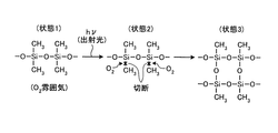
具体的に、図15を参照して、一重項酸素存在下におけるシリコーン樹脂の重合化反応について説明する。図15は、メチルレジン系シリコーン樹脂の変質メカニズムを説明するための図である。図15に示すように、酸素雰囲気において、メチル基を側鎖に有するメチルレジン系シリコーン樹脂(状態1)に、1270nm以下の波長領域を満足する波長の出射光を半導体レーザ310から出力すると、メチル基である側鎖を切って一重項励起状態の酸素と結合し(状態2)、主鎖を重合化する(状態3)。この結果、第1部分3120の樹脂密度が増加し、さらに透明樹脂320の光出射部3100近傍の第1部分3120の屈折率が、透明樹脂320の光出射部3100近傍以外の第2部分3130の屈折率よりも高くなるため、半導体レーザ310の出射光を光ファイバ330の光入射端部331に導く光導波路3200が形成される。
Specifically, the polymerization reaction of the silicone resin in the presence of singlet oxygen will be described with reference to FIG. FIG. 15 is a view for explaining the alteration mechanism of the methylresin-based silicone resin. As shown in FIG. 15, when emitted light having a wavelength satisfying a wavelength region of 1270 nm or less is output from a
ここで、出射光の照射条件を限定することによって、この光導波路3200の形成の効率化を図ることができる。出射光の照射条件としては、少なくとも出射光の波長、雰囲気温度、及び出射光の照射時間が挙げられる。また、少なくとも酸素分子を含む雰囲気で、酸素を活性化させる波長領域(1270nm)の強度を高めることができるように、出射光の波長及び雰囲気温度を調整する。
Here, the formation efficiency of the
まず、図16を参照して、図12に示す半導体レーザ310の出射光の波長及び雰囲気温度の関係を説明する。
First, the relationship between the wavelength of the emitted light of the
図16は、半導体レーザ310の光出射部3100から出力される出力光信号L31のパワーが、時間が経過するのに伴って上昇していく例を示す図である。図16では、雰囲気温度(環境温度ともいう)が0℃、−20℃、−40℃の場合を示している。
FIG. 16 is a diagram illustrating an example in which the power of the output optical signal L31 output from the light emitting unit 3100 of the
図16に示すように、雰囲気温度が下がるほど、時間に対して、出力光信号L31のパワーが大きい結果となった。これは、雰囲気温度が0℃のとき、出力光信号L31の波長は1290nm近傍となり、−20℃のとき、出力光信号L31の波長は1280nm近傍となり、−40℃のとき、出力光信号L31の波長は1270nm近傍となるためである。 As shown in FIG. 16, the power of the output optical signal L31 increases with time as the ambient temperature decreases. This is because when the ambient temperature is 0 ° C., the wavelength of the output optical signal L31 is near 1290 nm, when it is −20 ° C., the wavelength of the output optical signal L31 is near 1280 nm, and when it is −40 ° C., This is because the wavelength is in the vicinity of 1270 nm.
半導体レーザ310から出力される光信号L31の波長は、幅を持つため、雰囲気温度が0℃のとき、即ち、出力光信号L31の波長は1290nm近傍であっても、酸素を活性化させる1270nm以下の波長も有している。しかし、その分布量は、雰囲気温度が−40℃のときに比較して少ないため、透明樹脂320の第1部分3120の変質による樹脂密度の増加が小さい。そのため、雰囲気温度が下がるほど、時間に対して、出力光信号L31のパワーが大きくなった。
Since the wavelength of the optical signal L31 output from the
また、図16に示すように、雰囲気温度によって、時間に対して出力光信号L31のパワーの変化は、一定ではないことがわかる。このため、雰囲気温度によって、光結合効率が最適となる出射光の照射時間を、即ち、パワーが最大となる出射光の照射時間を調整し、これにより、透明樹脂320の第1部分3120の変質による樹脂密度を増加させる。
Further, as shown in FIG. 16, it can be seen that the change in the power of the output optical signal L31 with respect to time is not constant depending on the ambient temperature. For this reason, the irradiation time of the emitted light that optimizes the optical coupling efficiency, that is, the irradiation time of the emitted light that maximizes the power, is adjusted according to the ambient temperature, thereby changing the quality of the first portion 3120 of the
図12及び図14に示したように、半導体レーザ310が、1310nmの波長を有する出力光信号L31を出力する場合は、出射時間を調整するとともに雰囲気温度を室温よりも低温にすることにより、レーザ光のピーク波長を1310nmから1270nmに変化させることができる。このため、室温よりも低温である雰囲気温度下で半導体レーザ310からレーザ光を出射させることによって、このレーザ光のピーク波長を1270nmとして、この1270nmの波長のレーザ光に対応する出力光信号L31で、透明樹脂320の第1部分3120を効率よく変質させ、樹脂密度を増加させることができる。
As shown in FIGS. 12 and 14, when the
このように、半導体レーザ310から1270nmの波長を含むレーザ光を発することによって、半導体レーザ310と光ファイバ330の光入射端部331のコア332の端面が透明樹脂320の光導波路3200を通じて直接光結合されて、半導体レーザ310の出射光を光ファイバ330の光入射端部331へ導くための光導波路3200を形成することにより光結合効率を高めることができる。
In this way, by emitting laser light having a wavelength of 1270 nm from the
即ち、透明樹脂320の半導体レーザ310の光出射部3100の近傍の第1部分3120の樹脂密度を増加させることで、透明樹脂320の光出射部3100近傍の第1部分3120は、光信号L31により変質された透明樹脂320の変質部と呼ぶことができるとともに、透明樹脂320の光出射部3100近傍以外の第2部分3130は透明樹脂320の未変質部と呼ぶことができる。この変質部の光の屈折率は未変質部の光の屈折率に比べて高く、この変質部と未変質部との間には光の屈折率差があることから、透明樹脂320は、この屈折率差を利用して半導体レーザ310の光出射部3100と光ファイバ330の光入射端部331のコア332の端面の間に光導波路3200を形成できる。
That is, by increasing the resin density of the first portion 3120 in the vicinity of the light emitting portion 3100 of the
このように透明樹脂320では、半導体レーザ310の光出射部3100と光ファイバ330の光入射端部331のコア332の端面の間の変質部の第1部分3120が、それ以外の第2部分3130に比べて高屈折率化が可能になるので、半導体レーザ310から出力される出射光の照射条件を調整して出射光のピーク波長を1270nmにすることで、効率よく一重項酸素を発生さシリコーン樹脂の重合化反応を進めることで、変質部(第1部分3120)と未変質部(第2部分3130)との屈折率差が大きくなり、透明樹脂320における光導波路3200を形成できる。
As described above, in the
例えば、光モジュール301の置かれた雰囲気が室温よりも低温であれば、効率よく一重項酸素を生成できることから、変質部(第1部分3120)と未変質部(第2部分3130)との屈折率差が大きくなり、透明樹脂320における光導波路を確実に形成できる。
For example, if the atmosphere in which the
また、半導体レーザ310を駆動して、透明樹脂320に対して半導体レーザ310から出射光を発生するときに、出射光のピーク波長を1270nmにすることで、効率よく一重項酸素を発生させることができるため、透明樹脂320を変質させ、シリコーン樹脂の主鎖の架橋密度が上がって硬くなった光導波路効果が得られる。
In addition, when the
また、本発明の光モジュール301の透明樹脂320は、入手し易く加工が容易であるシリコーン樹脂であることから、半導体レーザ310と光ファイバ330の間の封止化も確実かつ簡易に行なうことができる。
In addition, since the
また、半導体レーザ310のLDチップとして分布帰還型半導体レーザ(DFB−LD)を用いて、半導体レーザ310からの出力される出射光のピーク波長を1270nmの波長に特定することにより、室温のままでも一重項酸素を効率よく発生させることができるため、透明樹脂320における光導波路3200を円滑に形成できる。
Further, by using a distributed feedback semiconductor laser (DFB-LD) as the LD chip of the
ところで、本発明は、上記実施形態に限定されず種々の変形例を採用できる。 By the way, this invention is not limited to the said embodiment, A various modified example is employable.
上述した図12及び図14に示す光モジュールの例では、半導体レーザ310から出力した1270nmの波長を含む出射光により、一重項酸素を発生させ、透明樹脂320の第1部分3120を変質させ、半導体レーザ310の光出射部3100と光ファイバ330の光入射端部331のコア332の端面との間に光導波路3200を形成しているが、図17に示すように、半導体レーザ310からだけでなく、光ファイバ330側からも、1270nmの波長を含む出射光を、光ファイバ330のコア332より出力することにより、光ファイバ330の光入射端部331のコア332の端面の間に光導波路3200を形成することもできる。
In the example of the optical module shown in FIG. 12 and FIG. 14 described above, singlet oxygen is generated by the emitted light including the wavelength of 1270 nm output from the
即ち、照射時間に対して、半導体レーザ310側から出射光による透明樹脂320の変質部3210の境界を光ファイバ330のコア332の端面に連続的に近づけるとともに、光ファイバ330側から1270nmの波長を含む出射光による透明樹脂320の変質部3220の境界を半導体レーザ310の光出射部3100に連続的に近づけることにより、半導体レーザ310の光出射部3100と光ファイバ330の光入射端部331のコア332の端面との間に光導波路3200となる、少なくとも変質部3210と変質部3220とを含む、変質した透明樹脂320の第1部分3120を短時間で形成することができる。
That is, with respect to the irradiation time, the boundary of the altered
また、例えば、図12に示す光モジュールの例では、光信号の送信と受信が可能な光送受信モジュールであるが、これに限らず、光モジュールは光信号を送信できる光送信モジュールであってもよい。 For example, in the example of the optical module shown in FIG. 12, the optical transmission / reception module is capable of transmitting and receiving an optical signal. However, the present invention is not limited to this, and the optical module may be an optical transmission module capable of transmitting an optical signal. Good.
また、図12に示すに光モジュール301は、出力光信号L31を発生して光ファイバ330を通じて出力し、光ファイバ330を通じて入力された入力光信号L32を受光できる。しかし、これに限らず、図18に示すように、半導体レーザ310と光導波路としての光ファイバ330Aを備えており、半導体レーザ310と光ファイバ330Aを直接光結合していて、半導体レーザ310と光ファイバ330Aの間が透明樹脂320により埋めてあるような構成であれば、本発明は適用できる。また、透明樹脂320の種類は、シリコーンに限らず、他の種類を採用できる。
In addition, as shown in FIG. 12, the
(その他の実施形態1)
つぎに、本発明の他の実施形態について説明する。図19は、本発明の他の実施形態1に係る光ファイバ接続構造の模式的な断面図である。この光ファイバ接続構造400は、コネクタフェルール401と、コネクタフェルール402とが、導波路フィルム403を介在させて突き合わせた状態で接続した構造を有している。コネクタフェルール401、402には、それぞれアレイ状に並べた4本の光ファイバ4011〜4014、4021〜4024が挿通固定されている。また、コネクタフェルール401、402は、不図示のラッチ構造またはクリップ等で互いに固定されている。ここで、導波路フィルム403には、たとえば酸化シリコンからなる変質部4031〜4034と、変質部4031〜4034よりも屈折率が低い、たとえばシリコーン樹脂からなる未変質部4035とが構成する光導波路が形成されている。そして、対向して配置された光ファイバ4011と光ファイバ4021は、変質部4031と未変質部4035とが構成する光導波路によって光学的に接続している。また、他の対向する光ファイバ同士もそれぞれ対応する光導波路によって光学的に接続している。なお、変質部4031〜4034の屈折率は1.46に近く、光ファイバ4011〜4014、4021〜4024と屈折率の整合がとれているため、変質部と光ファイバとの界面での反射はきわめて低く抑制されている。(Other embodiment 1)
Next, another embodiment of the present invention will be described. FIG. 19 is a schematic cross-sectional view of an optical fiber connection structure according to another
この光ファイバ接続構造400においては、導波路フィルム403に光導波路が形成されているので、従来の屈折率整合剤や屈折率整合シートを用いる場合と比較して、導波路フィルム403の厚さが厚くても接続損失が増大することがない。さらには、この導波路フィルム403は柔軟性を有するので、各光ファイバの端面の位置がばらついているなどの理由により、対向する光ファイバの端面間の距離がばらついていても、そのばらつきにかかわらず、導波路フィルム403が光ファイバの端面間を隙間なく埋めることができる。また、上述した光導波路の効果によって、光ファイバ同士はその端面間距離が大きくても、低接続損失で接続できる。たとえば、光ファイバの端面間の距離が1〜200μm程度であれば、その距離に応じた厚さの導波路フィルム403を用いることによって、その隙間を埋めることができるとともに、低接続損失が実現される。また、言い換えれば、この光ファイバ接続構造400は、各光ファイバの端面の加工精度が低くても、すなわち、端面の位置がばらついていたり、または端面の研磨精度が低かったりしても、低接続損失が実現できるので、低コストで製造できるものとなる。
In this optical
なお、この光ファイバ接続構造400は、たとえば以下のように製造することができる。図20は、図19に示す光ファイバ接続構造の製造方法の一例を説明する説明図である。図20に示すように、まず光ファイバ4011〜4014、4021〜4024が挿通固定されたコネクタフェルール401、402を準備し、これらを厚さ1〜200μm程度のシリコーン樹脂からなるフィルム基材404を介在させて突き合わせた状態で接続し、固定する。つぎに、アレイ光源等を用いて、光ファイバ4011〜4014のそれぞれの一端から、1270nmの波長を含むレーザ光L41を入力する。すると、レーザ光L41は光ファイバ4011〜4014のフィルム基材404に接する他端から出射されるので、フィルム基材404内で一重項酸素の発生により重合化反応等が起こり、酸化シリコンからなる変質部4031〜4034が徐々に形成され、光導波路が形成される。その結果、フィルム基材404は最終的に導波路フィルム403となり、光ファイバ接続構造400が完成する。
In addition, this optical
なお、レーザ光L41は、光ファイバ4021〜4024のそれぞれから入力してもよいし、光ファイバ4011〜4014と光ファイバ4021〜4024の両側から入力してもよい。また、導波路フィルム403およびフィルム基材404の材料は、シリコーン樹脂のみならず、PC、ポリエチレン等の樹脂でもよい。
The laser light L41 may be input from each of the
(他の実施形態2)
つぎに、本発明のさらに他の実施形態について説明する。図21は、本発明の他の実施形態2に係る光経路変換構造の模式的な断面図である。この光経路変換構造500は、光ファイバ501と、反射手段としての反射面の反射率を金蒸着等により高めた三角プリズム等のプリズム502と、フォトダイオード等の受光素子503と、導波路部材504とを備える。ここで、導波路部材504は、たとえば酸化シリコンからなる変質部5041、5042と、変質部5041、5042よりも屈折率が低い、たとえばシリコーン樹脂からなる未変質部5043から構成される光導波路が形成されている。変質部5041は、光ファイバ501から出射した光L51をプリズム502へ導波するように配置されている。また、プリズム502は、その反射面5021で光L51を反射し、光L51の伝搬方向を90度だけ回転するように配置されている。また、変質部5042は、表面5021で反射した光L51を受光素子503へ導波するように配置されている。すなわち、この光経路変換構造500は、光ファイバ501から出射した光L51の光路を90度だけ回転するような機能を有するものである。なお、光L51の波長は特に限定されないが、たとえば光ファイバ通信で最も用いられる波長1310nm近傍、あるいは1550nm近傍の光とすることができる。(Other embodiment 2)
Next, still another embodiment of the present invention will be described. FIG. 21 is a schematic cross-sectional view of an optical path conversion structure according to another
この光経路変換構造500は、たとえば以下のように製造することができる。図22は、図21に示す光経路変換構造の製造方法の一例を説明する説明図である。図22に示すように、まず光ファイバ501、プリズム502、受光素子503を所定の位置に配置し、これらの間をシリコーン樹脂からなる基材505で埋める。つぎに、光ファイバ501の一端から、1270nmの波長を含むレーザ光L52を入力する。すると、レーザ光L52は光ファイバ501の基材505に接する他端から出射されるので、基材505内で一重項酸素の発生により重合化反応等が起こる。その結果、酸化シリコンからなる変質部5041が徐々に形成され、さらに変質部5041がプリズム502に到るまで形成された後、変質部5042が徐々に形成され、光導波路が形成される。その結果、基材505は最終的に導波路部材504となり、光経路変換構造500が完成する。
The optical
この光経路変換構造500は、容易に形成できるとともに、レンズ等の光学系を用いなくても、光ファイバ501と受光素子503との光結合効率を高めることができるので、部材点数を削減でき、小型化かつ安価なものとなる。なお、反射手段は、プリズム502に限らず、金属ミラーや多層膜フィルタでもよい。また、光L51の回転角度も、90度に限らず、適宜設定できる。また、基材505および導波路部材504の材料は、シリコーン樹脂のみならず、PC、ポリエチレン等の樹脂でもよい。
The optical
なお、一重項酸素により重合反応を生じさせることができる樹脂については、メチルレジンシリコーン樹脂やメチルフェニルレジンシリコーン樹脂を例として述べたが、これらの樹脂にフィラーを添加する事により、架橋重合の程度を制御することができることが実験的に判っている。このことは、本発明の光導波路への応用において、最適な導波路構造を意図的に作製することができることを示唆している。 The resin capable of causing a polymerization reaction with singlet oxygen has been described as an example of a methyl resin silicone resin or a methylphenyl resin silicone resin. However, by adding a filler to these resins, the degree of crosslinking polymerization It has been experimentally found that can be controlled. This suggests that an optimum waveguide structure can be intentionally produced in the application of the present invention to an optical waveguide.
以下、図12と同様に半導体レーザを樹脂で封止し、1270nm近傍のレーザ光を出射して樹脂に通光させた場合と、未封止とした場合の実験結果について説明する。図23は、樹脂封止した半導体レーザの光放射遠視野像の半値全角θのフィラー添加量依存性を示す図である。なお、横軸は半導体レーザからのレーザ光を樹脂に通光させる時間を示し、縦軸は半値全角θを示している。また、樹脂としてはシリコーン樹脂を用いた。また、フィラーとしてはナノフィラーを用いた。 Hereinafter, similar to FIG. 12, the experimental results when the semiconductor laser is sealed with resin, the laser light near 1270 nm is emitted and transmitted through the resin, and the case where the laser is not sealed will be described. FIG. 23 is a diagram showing the dependency of the full width at half maximum θ of the resin-encapsulated semiconductor laser light emission far-field image on the amount of filler added. The horizontal axis indicates the time for passing the laser light from the semiconductor laser through the resin, and the vertical axis indicates the full width at half maximum θ. A silicone resin was used as the resin. Moreover, the nano filler was used as a filler.
この例では,未封止の半導体レーザの半値全角θが23°であるのに対し、ナノフィラーを無添加の樹脂の場合、樹脂に形成された光導波路端からの光放射の遠視野像の半値全角θは5°程度になる。一方、ナノフィラーを1%(重量比)添加した樹脂では半値全角θが10°で安定し、また、ナノフィラーを5%添加した樹脂では半値全角θが15°で安定することが判った。 In this example, the full width at half maximum θ of an unsealed semiconductor laser is 23 °, whereas in the case of a resin without addition of nanofillers, a far-field image of light emission from the end of the optical waveguide formed in the resin is used. The full width at half maximum θ is about 5 °. On the other hand, it was found that the resin added with 1% (weight ratio) of nanofiller was stable at a full width at half maximum θ of 10 °, and the resin added with 5% of nanofiller was stable at a full width at half maximum θ of 15 °.
図23に示す実験結果より、ある種のナノフィラーを添加することにより、一重項酸素による重合反応の程度を制御できると共に、重量比率を増やすことにより、重合反応部の屈折率変化を小さくすることができる。このようにフィラーの添加量を調整することにより,所望の光導波路構造を作ることができる。 From the experimental results shown in FIG. 23, it is possible to control the degree of polymerization reaction by singlet oxygen by adding a certain type of nanofiller, and to reduce the refractive index change of the polymerization reaction part by increasing the weight ratio. Can do. Thus, by adjusting the amount of filler added, a desired optical waveguide structure can be made.
なお、光導波路への応用においては、光透過性が必要なため、フィラーの成分はシリカ(SiO2)等が好ましく、その形状は、不定形またはコロイダルシリカのような球形のものが適用出来る。その寸法としては数nm〜数十nmのナノフィラーや、数十μmの大きさのマイクロフィラーがある。In addition, in application to an optical waveguide, since light transmittance is required, the filler component is preferably silica (SiO 2 ) or the like, and the shape can be indeterminate or spherical such as colloidal silica. The dimensions include nanofillers of several nm to several tens of nm and microfillers having a size of several tens of μm.
本発明は、活性化酸素を用いて局所的に材料の特性を変化させて所望の材料を製造する際に好適に利用できる。 INDUSTRIAL APPLICABILITY The present invention can be suitably used when a desired material is produced by locally changing the characteristics of the material using activated oxygen.
Claims (9)
Priority Applications (1)
| Application Number | Priority Date | Filing Date | Title |
|---|---|---|---|
| JP2009531308A JP5367576B2 (en) | 2007-09-07 | 2008-09-08 | Material manufacturing method |
Applications Claiming Priority (6)
| Application Number | Priority Date | Filing Date | Title |
|---|---|---|---|
| JP2007233348 | 2007-09-07 | ||
| JP2007233348 | 2007-09-07 | ||
| JP2008092346 | 2008-03-31 | ||
| JP2008092346 | 2008-03-31 | ||
| JP2009531308A JP5367576B2 (en) | 2007-09-07 | 2008-09-08 | Material manufacturing method |
| PCT/JP2008/066194 WO2009031685A1 (en) | 2007-09-07 | 2008-09-08 | Process for producing material |
Publications (2)
| Publication Number | Publication Date |
|---|---|
| JPWO2009031685A1 JPWO2009031685A1 (en) | 2010-12-16 |
| JP5367576B2 true JP5367576B2 (en) | 2013-12-11 |
Family
ID=40428996
Family Applications (1)
| Application Number | Title | Priority Date | Filing Date |
|---|---|---|---|
| JP2009531308A Active JP5367576B2 (en) | 2007-09-07 | 2008-09-08 | Material manufacturing method |
Country Status (5)
| Country | Link |
|---|---|
| US (1) | US20100160479A1 (en) |
| EP (1) | EP2186851A1 (en) |
| JP (1) | JP5367576B2 (en) |
| CN (1) | CN101796107B (en) |
| WO (1) | WO2009031685A1 (en) |
Families Citing this family (1)
| Publication number | Priority date | Publication date | Assignee | Title |
|---|---|---|---|---|
| US10338325B1 (en) * | 2018-06-01 | 2019-07-02 | International Business Machines Corporation | Nanofiller in an optical interface |
Citations (5)
| Publication number | Priority date | Publication date | Assignee | Title |
|---|---|---|---|---|
| JPH03128947A (en) * | 1989-10-14 | 1991-05-31 | I S I:Kk | Surface modification of material |
| JPH03128941A (en) * | 1989-10-14 | 1991-05-31 | I S I:Kk | Surface modification of material |
| JPH0559177A (en) * | 1987-11-12 | 1993-03-09 | Dow Corning Corp | Infusibilization of preceramic polymer by ultraviolet ray treatment |
| JPH11236460A (en) * | 1998-02-20 | 1999-08-31 | Dainippon Printing Co Ltd | Treatment of surface of plastic film |
| JP2001110802A (en) * | 1999-10-06 | 2001-04-20 | Matsushita Electric Ind Co Ltd | Method for forming insulation film |
Family Cites Families (3)
| Publication number | Priority date | Publication date | Assignee | Title |
|---|---|---|---|---|
| IT998906B (en) * | 1973-10-24 | 1976-02-20 | Snam Progetti | PROCEDURE FOR BENDING DEGRADABLE POLYMERS |
| US7404990B2 (en) * | 2002-11-14 | 2008-07-29 | Air Products And Chemicals, Inc. | Non-thermal process for forming porous low dielectric constant films |
| US20080020941A1 (en) * | 2005-03-24 | 2008-01-24 | Jimpei Tabata | Biomolecule-immobilized plate and method for fabricating biomolecule-immobilized plate |
-
2008
- 2008-09-08 EP EP08828984A patent/EP2186851A1/en not_active Withdrawn
- 2008-09-08 WO PCT/JP2008/066194 patent/WO2009031685A1/en active Application Filing
- 2008-09-08 JP JP2009531308A patent/JP5367576B2/en active Active
- 2008-09-08 CN CN2008801058229A patent/CN101796107B/en active Active
-
2010
- 2010-03-05 US US12/718,577 patent/US20100160479A1/en not_active Abandoned
Patent Citations (5)
| Publication number | Priority date | Publication date | Assignee | Title |
|---|---|---|---|---|
| JPH0559177A (en) * | 1987-11-12 | 1993-03-09 | Dow Corning Corp | Infusibilization of preceramic polymer by ultraviolet ray treatment |
| JPH03128947A (en) * | 1989-10-14 | 1991-05-31 | I S I:Kk | Surface modification of material |
| JPH03128941A (en) * | 1989-10-14 | 1991-05-31 | I S I:Kk | Surface modification of material |
| JPH11236460A (en) * | 1998-02-20 | 1999-08-31 | Dainippon Printing Co Ltd | Treatment of surface of plastic film |
| JP2001110802A (en) * | 1999-10-06 | 2001-04-20 | Matsushita Electric Ind Co Ltd | Method for forming insulation film |
Also Published As
| Publication number | Publication date |
|---|---|
| US20100160479A1 (en) | 2010-06-24 |
| WO2009031685A1 (en) | 2009-03-12 |
| JPWO2009031685A1 (en) | 2010-12-16 |
| EP2186851A1 (en) | 2010-05-19 |
| CN101796107A (en) | 2010-08-04 |
| CN101796107B (en) | 2012-08-22 |
Similar Documents
| Publication | Publication Date | Title |
|---|---|---|
| JP4564502B2 (en) | Method and apparatus for providing an optical beam output coupler | |
| JP4401540B2 (en) | Laser apparatus and optical signal amplifying apparatus using the same | |
| US10078181B2 (en) | Robust fiber cell for atomic and molecular sensing | |
| WO2006075760A1 (en) | Light source apparatus provided with modulating function and method for driving same | |
| US20030183152A1 (en) | Method of laser-assisted fabrication of optoelectronic and photonic components | |
| JP5367576B2 (en) | Material manufacturing method | |
| JP2018189875A (en) | Optical connection structure and forming method thereof | |
| US9395502B2 (en) | Apparatus and method for coupling optical signals between optical fibers and photo devices | |
| JP2010145767A (en) | Optical module | |
| CN103944060A (en) | Silicon photonics chip based on laser packaging | |
| JP2005215426A (en) | Semiconductor laser module | |
| JP4086496B2 (en) | Optical waveguide and optical waveguide manufacturing method | |
| JP4549575B2 (en) | Optical waveguide forming method and optical transceiver module | |
| Ozawa et al. | Self-written waveguide connection across diced waveguide gaps | |
| TWI264576B (en) | Optical waveguide apparatus | |
| JP2009080142A (en) | Optical module | |
| JP2004334003A (en) | Manufacture method of optical coupler and optical recording device | |
| JP2007322628A (en) | Method for splicing optical fiber | |
| CN113365775B (en) | Structure, method for manufacturing structure, laser device, and laser system | |
| US10209187B1 (en) | Method for atomic and molecular sensing | |
| KR102408995B1 (en) | Polymer waveguide accommodating dispersed graphene and method for manufacturing the same, and laser based on the polymer waveguide | |
| WO2022130692A1 (en) | Optical device, and method for manufacturing optical device | |
| JP4710046B2 (en) | Optical recording device | |
| JP5158869B2 (en) | Optical module | |
| JP2003098366A (en) | Optical waveguide and method for forming optical waveguide |
Legal Events
| Date | Code | Title | Description |
|---|---|---|---|
| A621 | Written request for application examination |
Free format text: JAPANESE INTERMEDIATE CODE: A621 Effective date: 20110601 |
|
| A131 | Notification of reasons for refusal |
Free format text: JAPANESE INTERMEDIATE CODE: A131 Effective date: 20130604 |
|
| A521 | Written amendment |
Free format text: JAPANESE INTERMEDIATE CODE: A523 Effective date: 20130801 |
|
| TRDD | Decision of grant or rejection written | ||
| A01 | Written decision to grant a patent or to grant a registration (utility model) |
Free format text: JAPANESE INTERMEDIATE CODE: A01 Effective date: 20130827 |
|
| A61 | First payment of annual fees (during grant procedure) |
Free format text: JAPANESE INTERMEDIATE CODE: A61 Effective date: 20130911 |
|
| R151 | Written notification of patent or utility model registration |
Ref document number: 5367576 Country of ref document: JP Free format text: JAPANESE INTERMEDIATE CODE: R151 |
|
| S531 | Written request for registration of change of domicile |
Free format text: JAPANESE INTERMEDIATE CODE: R313531 |
|
| R350 | Written notification of registration of transfer |
Free format text: JAPANESE INTERMEDIATE CODE: R350 |