JP5357547B2 - Method and system for detecting object position-based attributes using digital codes - Google Patents
Method and system for detecting object position-based attributes using digital codes Download PDFInfo
- Publication number
- JP5357547B2 JP5357547B2 JP2008541174A JP2008541174A JP5357547B2 JP 5357547 B2 JP5357547 B2 JP 5357547B2 JP 2008541174 A JP2008541174 A JP 2008541174A JP 2008541174 A JP2008541174 A JP 2008541174A JP 5357547 B2 JP5357547 B2 JP 5357547B2
- Authority
- JP
- Japan
- Prior art keywords
- electrodes
- signal
- electrode
- applying
- modulation signals
- Prior art date
- Legal status (The legal status is an assumption and is not a legal conclusion. Google has not performed a legal analysis and makes no representation as to the accuracy of the status listed.)
- Active
Links
Images


Classifications
-
- G—PHYSICS
- G06—COMPUTING; CALCULATING OR COUNTING
- G06F—ELECTRIC DIGITAL DATA PROCESSING
- G06F3/00—Input arrangements for transferring data to be processed into a form capable of being handled by the computer; Output arrangements for transferring data from processing unit to output unit, e.g. interface arrangements
- G06F3/01—Input arrangements or combined input and output arrangements for interaction between user and computer
- G06F3/03—Arrangements for converting the position or the displacement of a member into a coded form
- G06F3/041—Digitisers, e.g. for touch screens or touch pads, characterised by the transducing means
- G06F3/044—Digitisers, e.g. for touch screens or touch pads, characterised by the transducing means by capacitive means
-
- G—PHYSICS
- G06—COMPUTING; CALCULATING OR COUNTING
- G06F—ELECTRIC DIGITAL DATA PROCESSING
- G06F3/00—Input arrangements for transferring data to be processed into a form capable of being handled by the computer; Output arrangements for transferring data from processing unit to output unit, e.g. interface arrangements
- G06F3/01—Input arrangements or combined input and output arrangements for interaction between user and computer
- G06F3/03—Arrangements for converting the position or the displacement of a member into a coded form
- G06F3/041—Digitisers, e.g. for touch screens or touch pads, characterised by the transducing means
- G06F3/0416—Control or interface arrangements specially adapted for digitisers
- G06F3/0418—Control or interface arrangements specially adapted for digitisers for error correction or compensation, e.g. based on parallax, calibration or alignment
- G06F3/04182—Filtering of noise external to the device and not generated by digitiser components
-
- G—PHYSICS
- G06—COMPUTING; CALCULATING OR COUNTING
- G06F—ELECTRIC DIGITAL DATA PROCESSING
- G06F3/00—Input arrangements for transferring data to be processed into a form capable of being handled by the computer; Output arrangements for transferring data from processing unit to output unit, e.g. interface arrangements
- G06F3/01—Input arrangements or combined input and output arrangements for interaction between user and computer
- G06F3/03—Arrangements for converting the position or the displacement of a member into a coded form
- G06F3/041—Digitisers, e.g. for touch screens or touch pads, characterised by the transducing means
- G06F3/0416—Control or interface arrangements specially adapted for digitisers
- G06F3/0418—Control or interface arrangements specially adapted for digitisers for error correction or compensation, e.g. based on parallax, calibration or alignment
- G06F3/04186—Touch location disambiguation
-
- H—ELECTRICITY
- H03—ELECTRONIC CIRCUITRY
- H03K—PULSE TECHNIQUE
- H03K17/00—Electronic switching or gating, i.e. not by contact-making and –breaking
- H03K17/94—Electronic switching or gating, i.e. not by contact-making and –breaking characterised by the way in which the control signals are generated
- H03K17/96—Touch switches
- H03K17/962—Capacitive touch switches
Abstract
Description
本発明は、一般に、タッチパッドなどの位置または近接センサに関し、より詳細には、指、スタイラスまたは他の物体の位置に基づく属性を、ディジタル符号を使用して検出することができる装置、システムおよび方法に関する。 The present invention relates generally to position or proximity sensors such as touchpads, and more particularly to an apparatus, system, and system capable of detecting attributes based on the position of a finger, stylus or other object using a digital code. Regarding the method.
位置センサは、コンピュータ、携帯情報端末(PDA)、メディアプレーヤ、ビデオゲームプレーヤ、家電製品、携帯電話、公衆電話、POS端末装置、ATM、キオスクなどの入力装置として一般に使用されている。このような用途で使用されるセンサの一般的なタイプとしてタッチパッドセンサがあり、例えば、多くのノートブック型のコンピュータの入力装置として簡単にみつけることができる。ユーザは、通常、センサの検知領域の近くで指、スタイラスまたは他の刺激を移動させることによって、センサを操作する。刺激が、検知領域に印加されているキャリア信号に容量性、誘導性、またはその他の電気的効果を引き起こし、これが検知され、検知領域に対する刺激の位置または近接度と相関されうる。今度は、この位置情報を、ディスプレイ画面上のカーソルまたはその他の標識を移動させたり、画面上の文字要素をスクロールしたり、それ以外のユーザインタフェース用途に使用することができる。キャパシタンス式の検知法に基づくタッチパッド型の位置センサの一例が、1999年3月9日にギレスピー(Gillespie)らに付与された米国特許第5,880,411号公報に記載されている。 The position sensor is generally used as an input device such as a computer, a personal digital assistant (PDA), a media player, a video game player, a home appliance, a mobile phone, a public telephone, a POS terminal device, an ATM, and a kiosk. A common type of sensor used in such applications is a touchpad sensor, which can be easily found, for example, as an input device for many notebook computers. A user typically operates a sensor by moving a finger, stylus, or other stimulus near the sensing area of the sensor. The stimulus causes a capacitive, inductive, or other electrical effect on the carrier signal applied to the sensing region, which can be detected and correlated with the location or proximity of the stimulus relative to the sensing region. This position information can now be used for moving a cursor or other indicator on the display screen, scrolling character elements on the screen, or other user interface applications. An example of a touchpad type position sensor based on a capacitance type sensing method is described in US Pat. No. 5,880,411 issued to Gillespie et al. On March 9, 1999.
タッチパッド型のセンサは数年にわたり使用されているものの、コストの削減および/またはセンサ能力の改善を実現する別の設計が求められている。より詳細には、近年、ディスプレイ画面、電源、無線周波干渉および/またはセンサの外のほかの発生源が発生させるノイズの影響を低減させることに多大な関心が寄せられている。サンプリング、フィルタリング、信号処理、シールドやその他の雑音低減法が数多く実装されているが、成果の程度はさまざまに異なる。 While touchpad type sensors have been in use for several years, there is a need for alternative designs that can reduce costs and / or improve sensor capabilities. More particularly, there has been much interest in recent years in reducing the effects of display screens, power supplies, radio frequency interference and / or noise generated by other sources outside the sensor. Numerous sampling, filtering, signal processing, shielding and other noise reduction methods have been implemented, but with varying degrees of success.
したがって、ノイズの存在下で物体の位置に基づく属性を迅速、効果的かつ効率的に検出するためのシステムおよび方法を提供することが望ましい。ほかの望ましい特徴および性質は、添付の図面と上記の技術分野と背景技術を併せて読めば、下記の詳細な説明と添付の特許請求の範囲から明らかとなるであろう。 Accordingly, it would be desirable to provide a system and method for quickly, effectively and efficiently detecting attributes based on the position of an object in the presence of noise. Other desirable features and characteristics will become apparent from the following detailed description and the appended claims, taken in conjunction with the accompanying drawings and the foregoing technical field and background.
タッチパッドまたは他のセンサによって、指、スタイラスまたは他の物体の位置に基づく属性を検出するための方法、システムおよび装置について記載する。さまざまな実施形態によれば、このセンサは、ユーザ入力を検出するために適切に配置されている任意の数の電極から構成されたタッチセンス領域を有する。1つ以上の電極に対する変調信号が、任意の数の異なる別個のディジタル符号の関数として作成され、これらの符号は互いに実質的に直交しうる。物体の位置によって電気的に影響された結果信号を得るために、複数の電極の関連する少なくとも1つに変調信号が印加される。物体によって引き起こされた電気的効果を選別するために、複数の別個のディジタル符号を使用して結果信号が復調される。電気的効果から、複数の電極に対する物体の位置に基づく属性が決定される。 A method, system, and apparatus for detecting attributes based on the position of a finger, stylus, or other object with a touchpad or other sensor are described. According to various embodiments, the sensor has a touch-sensitive area composed of any number of electrodes that are suitably arranged to detect user input. Modulation signals for one or more electrodes are generated as a function of any number of different discrete digital codes, which codes can be substantially orthogonal to each other. In order to obtain a result signal that is electrically influenced by the position of the object, a modulation signal is applied to at least one of the associated electrodes. The result signal is demodulated using a plurality of separate digital codes to screen out the electrical effects caused by the object. From the electrical effect, an attribute based on the position of the object relative to the plurality of electrodes is determined.
以下、図面を参照して本発明のさまざまな態様を記載する。図面において同じ参照符号は類似する要素を参照している。 Various aspects of the invention will now be described with reference to the drawings. In the drawings, like reference numerals refer to similar elements.
以下の詳細な説明は、本来例示的なものに過ぎず、本発明または本発明の用途および利用を限定することを意図したものではない。更に、上記の技術分野、背景技術、発明の開示、あるいは以下の詳細な説明に明示または暗示した理論により拘束されることを意図するものではない。 The following detailed description is merely exemplary in nature and is not intended to limit the invention or the uses and uses of the invention. Furthermore, there is no intention to be bound by any expressed or implied theory presented in the preceding technical field, background art, invention disclosure or the following detailed description.
さまざまな例示的な実施形態によれば、ノイズ余裕度の改善および/または性能向上のために、タッチパッドなどの位置センサに、広帯域スペクトラム技術が適用されうる。例えば、符号分割多重化(CDM)を使用して2つ以上の別個の変調信号を生成し、これがセンサ内の検知電極に印加され、これにより、印加された信号の有効電力を向上させることができる。符号化広帯域スペクトラム変調とは、ダイレクトシーケンス、周波数ホッピング、時間ホッピングまたはこれらの技術のさまざまな組み合わせを指しうる。センス領域に適用される変調周波数が、以前に受信されたよりも広範なスペクトルにわたっているため、特定の周波数で生じる狭帯域のノイズまたは中程度の広帯域ノイズ(これらは符号化変調とは無相関である)が、狭い復調信号チャネル全体に及ぼす影響が最小限とされる。また、有用な各信号チャネルについて最小信号対雑音比(SNR)が維持されるように、複数の信号チャネルに対するノイズの影響が平均化されうる。この概念は、既知の雑音源を回避する周波数領域信号を作成するためのディジタル符号を選択することにより、更に活用することができる。このため、広帯域スペクトラム技術により、検知領域に印加する電力を増加させる一方で、ノイズの影響を低減させることができ、相当するサンプル期間の従来の時間領域多重化技術と比較して、センサのSNRが大幅に改善される。センサに広帯域スペクトラム技術を適用することによって、他の有益なセンサ設計および機能も可能となる。このような概念を、以下により詳しく説明する。 According to various exemplary embodiments, wideband spectrum technology may be applied to a position sensor such as a touchpad to improve noise margin and / or performance. For example, code division multiplexing (CDM) may be used to generate two or more separate modulated signals that are applied to a sensing electrode in the sensor, thereby improving the effective power of the applied signal. it can. Coded wideband spectrum modulation may refer to direct sequence, frequency hopping, time hopping, or various combinations of these techniques. The modulation frequency applied to the sense domain spans a wider spectrum than previously received, so narrowband noise or moderate wideband noise that occurs at a particular frequency (these are uncorrelated with coded modulation) ) On the entire narrow demodulated signal channel is minimized. Also, noise effects on multiple signal channels can be averaged so that a minimum signal-to-noise ratio (SNR) is maintained for each useful signal channel. This concept can be further exploited by selecting a digital code to create a frequency domain signal that avoids known noise sources. For this reason, wideband spectrum technology can increase the power applied to the sensing region while reducing the effect of noise, and compared to the conventional time domain multiplexing technology of the corresponding sample period, the SNR of the sensor Is greatly improved. Other useful sensor designs and functions are also possible by applying broadband spectrum technology to the sensor. Such a concept will be described in more detail below.
本明細書で使用するように、「位置センサ」との文言は、従来のタッチパッド装置だけではなく、1本以上の指、ポインタ、スタイラスまたはその他の物体の位置または近接度を検出することができる、広い範囲の同等の装置も含むことを理解すべきである。このような装置としては、タッチスクリーン、タッチパッド、タッチタブレット、生物測定認証装置(指紋センサなど)、手描きまたは文字認識装置などが挙げられるが、これらに限定されることはない。同様に、ここで用いられる「位置」、「物体位置」および「位置に基づく属性」との文言は、絶対的または相対的な位置または近接度の情報のほか、速さ、速度、加速度などのほかのタイプの空間ドメイン情報も含むことを意図しており、これには、1つ以上の方向における移動の測定値が含まれる。さまざまな位置に基づく属性には、ジェスチャ認識などの場合のように、時間履歴の成分が含まれていてもよい。したがって、用途によって決定される別ではあるが同等の多様な実施形態において、多くの異なるタイプの「位置センサ」が、単なる物体の有無だけではなく、多種多様な「位置に基づく属性」を検出することができる。 As used herein, the term “position sensor” refers to detecting the position or proximity of one or more fingers, pointers, styluses or other objects, as well as conventional touchpad devices. It should be understood that a wide range of equivalent devices is also included. Such devices include, but are not limited to, touch screens, touch pads, touch tablets, biometric authentication devices (such as fingerprint sensors), hand-drawn or character recognition devices, and the like. Similarly, the terms “position”, “object position”, and “position-based attributes” as used herein refer to absolute or relative position or proximity information as well as speed, speed, acceleration, etc. It is intended to include other types of spatial domain information, including measurements of movement in one or more directions. The attributes based on various positions may include a component of time history as in the case of gesture recognition. Thus, in different but equivalent embodiments as determined by application, many different types of “position sensors” detect a wide variety of “position-based attributes”, not just the presence or absence of objects. be able to.
ここで図面を参照する。最初に図1Aを参照すると、例示的なセンサ100は、検知領域101、コントローラ102、関連する駆動回路109を有する変調器107、および関連する受信回路115を有する復調器117を適宜備える。指、スタイラスまたはその他の物体121の位置に基づく属性が、電極112A〜Dにさまざまな変調信号110A〜Dを印加することによって検出され、電極112A〜Dは、検知電極114と共に検知領域101を画定している。変調信号110A〜Dは、1つ以上の受信電極114に、容量または他の方式で電気的に結合されており、任意の数のデータ伝送チャネル113A〜Dを形成している。物体121によってチャネル113A〜Dに引き起こされる電気的効果が、その後、受信電極によって受信される信号116において識別される。この受信信号は、検知領域101内の電極112A〜Dに対する物体121の位置を分離するために、その後処理されうる。タッチパッドにおける容量検知と物体位置の処理の従来技術の例は、上に挙げた米国特許第5,880,411号明細書に記載されているが、多様な別の実施形態において、他の検知技術を使用することもできる。
Reference is now made to the drawings. Referring initially to FIG. 1A, an
さまざまなタイプのセンサ100が、物体121によって引き起こされるさまざまな電気的効果を検出することができるが、図1A〜Bの例示的な実施形態は、物体121の有無によって引き起こされる、検知領域101両端のキャパシタンスの変化を監視するための構成を示す。より詳細には、電極112A〜Dに変調信号110A〜Dが印加されると、「仮想のコンデンサ」が、被変調信号を送信している各電極112A〜Dと受信電極114の間に形成される。このコンデンサによって作成される場の中に物体が存在する場合、送信電極112と受信電極114間のキャパシタンスが影響を受ける。通常、指などの接地されている(または事実上接地されている)物体が存在する場合には、電極112と114間の実効キャパシタンスが低下し、接地されていない導体(スタイラスなど)や高誘電性の物体が存在する場合には、実効キャパシタンスが上昇する。いずれの場合も、物体121の存在によって引き起こされるキャパシタンスの変化が、受信電極114からの、測定された電圧、電流、電荷などの出力信号116に反映される。
Although various types of
各変調信号110A〜Dによって発生する信号116を監視することにより、各電極112A〜Dに対して物体121の存在を決定することができる。図1Aに示す例示的な実施形態では、4つの検知チャネル113A〜Dが、一次元の検知アレイ101に配置されて示される。図1Bの例示的な実施形態では、7つのチャネル113A〜Gが、112A〜Cと114の間の第1の方向に存在する数個のチャネル113A〜Cと、112D〜Gと114の間の実質的に直交する方向に存在する残りのチャネル113D〜Gとによって示されており、図4を参照して下記に詳しく説明するように、二次元の像の「シルエット」の検出が可能となっている。実際には、多様な別の実施形態では、わずか1つ、十数、あるいは、何百またはそれ以上の数の検知チャネルが、1つのパターンや複数次元のパターンに配置されてもよい。適切に配置を行えば、さまざまな電極に印加される変調信号110A〜Dを送信した際に、物体121によって引き起こされる電気的効果から、検知領域101に対する物体121の位置を決定することができる。この影響が、受信信号116に反映されて、これが復調され、その後適宜処理されて、出力信号120に到達する。
By monitoring the
更に、変調信号110を生成するためのディジタル符号の割り当てや再割り当てを行うことによって、センサ100を容易に構成または再構成して、領域101に任意のタイプまたは任意の数の検知ゾーンを作成することができる。図1A〜Bに示すように、各受信電極114は、任意の数の信号チャネル113によって結合された信号を受信することができ、これにより、1つの経路に複数の結果信号116が供給される。信号116が共有の経路に供給されるため、検知ゾーンを構成している送信電極112のそれぞれに、共通の変調信号110(共通のディジタル符号から形成された変調信号110など)を印加するだけで、任意の数の電極の検知チャネル113を恒久的または一時的に形成することができる。領域101内の検知ゾーンは、重複および/または経時変化してもよく、1つ以上の電極112に別のディジタル符号を印加するだけで、容易に再構成可能である。複数の電極が1つのチャネルの一部であっても、複数のチャネル変調が1つの電極に印加されてもよい。
In addition, the
従来のセンサでは、変調信号110A〜Dは、通常、単純なサイン波または他の周期的な交流(AC)信号であり、何らかの時間領域多重化(TDM)を使用して、さまざまなチャネルに逐次的に印加される。しかし、無線通信に一般に関連する広帯域スペクトラムの概念をセンサ100に適用することによって、数多くの利点を実現することができる。より詳細には、符号分割多重アクセス方式(CDMA)無線通信に使用されるものと同様のディジタル符号化技術を使用して、別個の変調信号110A〜Dを作成し、これらの信号を領域101のさまざまな検知ゾーンに同時に印加することができ、これにより、センサ100の切り替えを簡略化できる可能性がある。
In conventional sensors, the modulation signals 110A-D are typically simple sine waves or other periodic alternating current (AC) signals that are sequentially applied to various channels using some time domain multiplexing (TDM). Applied. However, many advantages can be realized by applying the broadband spectrum concept generally associated with wireless communications to the
広帯域スペクトラム技術をセンサ100に適用すると、ノイズ抵抗の改善など、追加の利点を提供することができる。各信号チャネル113が、適切なディジタル符号を印加することにより得られるため、例えば、符号化利得の原理を容易に利用して、センサ100の能力を改善することができる。符号を長くすると、1つ以上の送信電極112に印加される各変調信号110のゲインが増加する。従来の符号生成技術を用いることによって、周知のスペクトルおよび相関特性を有するディジタル符号の組み合わせのバリエーションを比較的容易に作り出すことができる。更に、これらの組み合わせのバリエーションにより、別個のディジタル符号の比較的大きな集合が形成され、ここから、以下で説明するように、望ましい時間領域または周波数領域の特性を有する変調信号110を生成することができる。特定の符号生成技術および信号処理技術に関するその他の詳細は、後で更に詳細に説明する。
Applying wideband spectrum technology to the
再び図1A〜Bを参照すると、検知領域101は、指、スタイラスまたは他の物体121の位置、近接度および/またはその他の位置に基づく属性を検出することができる容量型、抵抗型、誘導型のセンサ、あるいは他のタイプのセンサである。例示的な検知領域101は、米国カリフォルニア州サンタクララ所在のシナプティクス・インク(Synaptics Inc.)が製造している各種センサを備える。このセンサは、容量結合または誘導結合を使用して、物体121の一次元、二次元または多次元の位置を適切に検出する。しかし、多様な別の実施形態では、ほかの多くの検知領域101が使用されてもよい。位置または近接を検出することができるほかのタイプの検知領域101は、音響、光学または電磁的な特性(例えば高周波、赤外線、紫外線など)および/またはその他の効果に基づいたセンサを備える。
Referring again to FIGS. 1A-B, the
コントローラ102は、任意のプロセッサ、マイクロコントローラ、ニューラルネットワーク、アナログコンピュータ、プログラム済み回路、あるいは入力データ118を処理して、出力の指標120を抽出することが可能な他のモジュールなどである。使用される特定の制御回路102は、実施形態によって大きく変わるが、例示的な実施形態では、コントローラ102は、米国カリフォルニア州サンタクララ所在のシナプティクス・インク(Synaptics Inc.)が製造しているモデルT1004、T1005、T10XXまたは他のマイクロコントローラである。多くの実施形態では、コントローラ102は、ここに記載のさまざまな検知、制御およびその他の機能を実装するために、コントローラ102によって実行可能なディジタル命令を、ソフトウェアまたはファームウェアの形式で適切に記憶するディジタルメモリ103を備えるか、またはこれと通信するか、この両方を行う。別の実施形態では、メモリ103の機能がコントローラ102に組み込まれてもよく、すべての実施形態において、物理的に独立したメモリデバイス103が存在するとは限らない。物理的なコントローラが、更に多くの要素を備えていてもよく、これには、駆動回路109、受信回路115やその他の記載のものなどがある。
The
符号生成モジュール104は、任意の独立しているか、あるいは一体化された回路、デバイス、モジュール、プログラム論理などであり、変調信号110A〜Dの生成に使用されうるディジタル符号106を作成することができる。作成されるディジタル符号の数、サイズおよびタイプは大きく変わるが、さまざまな実施形態では、これら符号は互いに実質的に直交しており、領域101の各検知ゾーンに関連付けるのに十分な数の別個のディジタル符号を提供するのに十分な長さを有する。この別個の符号は、2値、3値または一般的にマルチレベルであり、駆動状態と非駆動状態を表すことができる(トライステート)。CDMとの併用に適したディジタル符号を生成するための各種回路、モジュールおよび技術には、ウォルシュアダマール符号、m−シーケンス、ゴールド符号、カサミ符号、バーカー符号、遅延ラインの複数のタップシーケンス(delay line multiple tap sequences)などのシフトレジスタシーケンスがある。別の実施形態では、ディジタル符号は予め決められており、コントローラ102および/またはメモリ103内のルックアップテーブルまたは他のデータ構造に記憶されていても、任意の適切なアルゴリズムを使用してコントローラ102によって生成されても、この両方でもよい。このような実施形態では、符号生成モジュール104が、コントローラ102とは独立した物理的な要素として存在しなくてもよく、コントローラ102または他のディジタル処理装置によって適宜実行される符号の生成および/または取得の機能を表す論理モジュールとして考えるべきである。
別個のディジタル符号の文脈において、「実質的に直交する」との文言は、別個の符号から、意味のある独立した結果が得られるのであれば、この別個の符号が、数学的な意味で互いに完全に直交していなくてもよいことを指す。このため、相関、スペクトルまたは圧縮性などのさまざまなほかの特性のために、厳密な直交性が犠牲にされうる(トレードオフ)。同様に、「検知ゾーン」との文言は、個々の電極112のいずれもよりも大きな検知領域101部分を含む1つのセンスゾーンを作成するために、複数の電極112に1つの符号が印加されうることを指す。また、1つの電極に複数の符号を印加して、重複するかまたは空間的にフィルタされた「検知ゾーン」を作成してもよい。例えば、同じ符号シーケンスを位相遅延または「シフト」したシーケンスは、別個であり、実質的に直交し、容易に識別可能でありうる。さまざまなケースでは、位相シフト間の補間が可能であってもよい。
In the context of separate digital codes, the phrase “substantially orthogonal” means that separate codes are mutually connected in a mathematical sense if they provide meaningful and independent results. It means that it does not have to be completely orthogonal. Thus, strict orthogonality can be sacrificed (tradeoff) due to various other characteristics such as correlation, spectrum or compressibility. Similarly, the term “sensing zone” can be applied to a plurality of electrodes 112 to create a single sensing zone that includes a
変調器107は、モジュール104が生成した別個のディジタル符号を使用して、変調信号110A〜Dを生成することができる任意の回路、論理または他のモジュールである。一般に、変調器107は、任意のタイプの振幅変調(AM)、周波数変調(FM)、位相変調(PM)または他の適切な技術を使用して、キャリア信号111をディジタル符号106によって変調して、変調信号110A〜Dを生成する。したがって、変調器107は、従来の任意のディジタルおよび/またはアナログ回路を使用して実装されても、コントローラ102などの内部で実行されるソフトウェア論理によって、その一部または全体が実装されてもよい。キャリア信号111は、任意のオシレータまたは他の信号発生器105によって適宜作成されうる。容量検知型のタッチパッドでの使用に適した一実施形態では、信号111は、約10kHz〜100MHzの範囲の周波数で作成されうるが、多様な同等の実施形態では、これらの信号がどのような周波数または範囲で作成されてもよい。例示的な変調機能に関する更に詳しい詳細は、後で図3を参照して説明する。更に別の実施形態では、キャリア信号111が省略されており、印加される変調信号110A〜Dのスペクトル成分が、ディジタル符号のクロック速度、繰り返し長さおよび/または他の性質から決定される。このため、さまざまな別の実施形態では、キャリア信号111が省略されるか、直流(DC)信号として概念的に解釈されるか、この両方が行われうる。
変調信号110A〜Dは、検知領域101の電極112A〜Dにどのように印加されてもよい。さまざまな実施形態においては、変調器107が、任意の駆動回路109を介して、適切な電極112A〜Dに信号を適宜印加し、駆動回路109には、任意のスケーリング増幅器、マルチプレクサ、任意の電流源または電圧源へのスイッチ、電荷転送素子、制御されたインピーダンスなどが含まれる。図1には、ドライバ回路109が、変調器107と検知領域101を直列に相互に接続しているように図示されている。しかし、実際には、駆動回路109は、通常、複数の増幅器、複数のドライバおよび/または他の信号路を備え、変調器107と検知領域101内のさまざまな電極112間を並列に接続しており、複数の検知チャネル113が、被変調電極112により、同じか、または異なる信号によって同時に駆動されるようになっている。
The modulation signals 110A to 110D may be applied to the
上で説明したように、検知領域101内の電極112A〜Dに変調信号110A〜Dが供給され、これにより得られた受信電極114からの結果信号(resultant signal)116が、適切な復調器117に供給される。スケーリング増幅器、マルチプレクサ、フィルタ、選別器、比較器および/または他の受信回路115も設けて、受信信号116を形成してもよい。復調器117は、物体121によって引き起こされた電気的効果を識別するために、検知領域101の出力116を復調することができる任意の回路または他のモジュールである。復調器117は、任意の適切なディジタルまたはアナログのローパスまたはバンドパスフィルタや、任意の従来のアナログ−ディジタル変換器(ADC)などの復調フィルタを有するか、これと通信するか、この両方を行いうる。さまざまな実施形態では、復調器117は、キャリア信号111、および/または位相シフトされた別個のディジタル符号106を受信して、この両方の信号の復調を可能にする。別の実施形態では、復調器117は、キャリア信号111をアナログ復調し、その後の処理のために、コントローラ102および/または受信回路115に、これにより得られた結果信号を提供する。同様に、図1のモジュール117によって表される復調機能は、コントローラ102および/または他の要素内のハードウェア、ソフトウェア、ファームウェアなどによって論理的に提供されてもよく、この場合、独立した復調回路117が不要となる。
As described above, modulation signals 110A-D are supplied to
センサ100の動作中に、任意の数の別個のディジタル符号が、符号生成モジュール104によって作成されて、キャリア周波数によって変調され、変調信号112A〜Dの組が生成され、これが検知領域101の任意の数の電極112A〜Dに印加される。検知領域101に対する物体121の位置が、検知領域101から供給される1つ以上の出力信号116に電気的に影響する。結果信号116を復調することによって、電気的効果が識別され、これがその後コントローラ102などによって処理されて、物体121に対する位置に基づく属性が決定される。電極を適切なディジタル符号によって変調することにより、センサの狭い検知周波数を、複数の周波数にわたって有効に拡散させることができ、ノイズ除去が改善される。更に、符号分割多重化を使用することによって、各変調信号110A〜Dを同時に印加することができ、これにより、多くの実施形態で、独立した時間領域の切り替えまたは制御の必要性を減らすか、なくすことができる。広帯域スペクトラム技術を使用して検知領域101から識別された電気的効果が、コントローラ102および/または他の処理装置によって、適切に更に処理されうる。
During operation of the
次に図2を参照すると、検知領域101に対する位置に基づく物体の属性を検出するための例示的処理200は、変調信号110A〜Dのために別個のディジタル符号の組を作成するステップ(ステップ201)と、変調信号110A〜Dを印加して得られた応答信号116のそれぞれを復調するステップ(ステップ204,206)と、応答信号116内で識別された電気的効果から、物体121の位置に基づく属性を1つ以上決定するステップ(ステップ208)と、の広いステップを適宜有する。さまざまな更に別の実施形態では、ノイズの影響を低減させるか、当該装置によって引き起こされるほかの装置への干渉を低減させるか、あるいはその他の目的のために、ステップ202で生成された特定のディジタル符号が変更されてもよい(ステップ210)。また、1つまたは複数の物体の処理、望ましくない像データの除去などの追加の処理も実行されうる(ステップ212)。
Referring now to FIG. 2, an
図2に示すフローチャートは、厳密なソフトウェアの実装ではなく、例示的な処理200に含まれるさまざまな論理的なステップを示すものである。しかし、プロセス200のステップの一部またはすべては、メモリ103内に記憶されており、コントローラ102のみによって実行されるか、センサ100のほかの要素(例えば、符号生成モジュール104、変調器107、復調器117など)と連動して実行されるか、この両方が行われてもよい。あるいは、さまざまなステップが、任意のディジタルメモリ、可搬媒体(例えば、コンパクトディスク、フロッピーディスク、ポータブルメモリなど)、磁気メディアまたは光メディアなどの任意のディジタル記録媒体に記憶されてもよい。多様な別の実施形態では、プロセス200の各種ステップが、時間的にどのような順序で適用されたり、あるいは他の方法で任意に変更されてもよい。更に、図2に示す各種ステップ同士を組み合わせたり、あるいは各種ステップがほかの方法で異なって編成されてもよい。
The flowchart shown in FIG. 2 illustrates the various logical steps involved in the
上で説明したように、変調信号110A〜Dの生成に使用される別個のディジタル符号106は、図1の符号生成モジュール104によって表される任意のタイプのハードウェアまたはソフトウェア論理によってなど、どのように生成されてもよい(ステップ201)。例えば、所望の長さの疑似ランダムディジタル符号を生成するために、任意の数のフィードバックシフトレジスタが、最大長シーケンス(MLS)に構成されてもよく、この疑似ランダムディジタル符号は、別個の符号シーケンスとして、さまざまな位相および/またはサム(sum)で、各種変調信号110A〜Dに容易に印加することができる。並列シフトレジスタから出力される二進符号のシーケンス106は、最小のDC項を除き、一般にスペクトルが平坦である。代替の実施形態では、ディジタル符号106を生成するためのMLSまたは他のルーチンが、適宜コントローラ102やその他で実行されているソフトウェアでシミュレーションされてもよい。更に別の実施形態では、符号106は、使用前に生成され、メモリ103内のルックアップテーブルまたは他のデータ構造などに記憶される。別ではあるが同等のさまざまな実施形態では、コントローラ102は、符号106を直接生成するか取得しても、独立した符号生成モジュール104などの動作を指示することによって符号を作成しても、この両方を行ってもよい。上で説明したように、特定の符号はどのように生成されてもよい。複数の別個の符号を作成するために、ディジタルビットのシーケンスを単に位相シフトさせてもよい。別の実施形態では、加算、排他論理和、乗算、および/または高次元数の乱数および擬似乱数を生成する他の技術などのさまざまな方法を使用して、別個の符号を別の符号から計算することができる。排他論理和または乗算の演算に基づく符号生成法には、線形の組み合わせを生成できる追加の利点があり、これが一部の実施形態では有用となりうる。
As explained above, the separate
次に、さまざまな符号106を使用して、特定の変調信号110A〜Dが変調されるか、または他の方法で生成され、これが、検知領域101のさまざまな検知電極112A〜Dに印加される(ステップ202)。上で説明したように、印加された信号は、物体121の存在によって電気的に影響され、生じた電気的効果が、受信信号116から決定される(ステップ203)。
Next,
(ステップ204における)受信信号チャネル113の復調では、被変調信号から、物体121の位置に関する情報が適宜抽出される。この抽出では、一般に、上に記載した変調プロセスが逆に実行される。したがって、復調器117は、以前に、特定の結果信号116を生成するためにキャリア信号の変調に使用された特定のディジタル符号106のほかに、通常、アナログ復調および/または信号選別(ノイズと所望の信号を選別するなど)を実行するためのキャリア信号111(または信号111と同期している他の信号)を受信する。センサが送信と受信の両方を行うため、キャリアまたは符号シーケンスの回収の必要はほとんどない。
In demodulation of the received signal channel 113 (in step 204), information regarding the position of the
任意の数の受信信号チャネル113に対して、復調が適宜実行されうる(ステップ206)。図1Aに示す例示的なセンサ100では、被変調電極112A〜Dから各信号チャネルを送信して得られた信号116が、受信電極114から出る共通パスで受信される。しかし、検知チャネル113A〜Dが、すべて同時に駆動されている(各被変調電極112A〜Dに変調信号110A〜Dが同時に提供されているなど)場合であっても、従来のCDM復調技術を使用して、各チャネル113A〜Dが生成した結果信号116を復調することができる。このため、任意の変調信号110A〜Dに対して生成される、結果信号116の特定の成分(またはチャネル)を、容易に抽出することができる。以下で説明するように、この概念は、センサ100に多くの追加機能と性能向上を与えるために、数多くの方法で利用することができる。例えば、領域101内の特定の検知ゾーンを拡げるために、複数の電極112A〜Dに共通の変調信号110A〜Dが印加されうる。このゾーンは、各種の動作モードを作り出すなどのために、動作中に容易に調整することができる。例えば、検知領域101全体が1つのボタンとして動作し、それ以外の点ではセンサの能力が調整されないようにするために、各電極112A〜Dに同じ変調信号110が提供されうる。受信電極116から得られる信号のすべてが図1の共通パスに供給されるため、この場合は、共通の変調符号を使用して受信信号の全体を復調するだけで、検知領域101内のどの場所でも物体121の存在を識別できる。同様の概念を適用して、ディジタル符号シーケンス106の単純な操作によって、検知領域101にわたり、任意の数の別個の検知ゾーンを作成したり、重複する検知ゾーンを作成することができる。更に、例えば手のひらを排除したり、他の不適当な入力を受けつけないようにするために、適切な変復調のみによって空間周波数フィルタリングを行うことができる。
Demodulation may be performed as appropriate for any number of received signal channels 113 (step 206). In the
物体121の位置に基づく属性を決定できるように、コントローラ102で復調信号118が適切に受信される(ステップ208)。これらの信号は、線形フィルタおよび非線形フィルタを使用して、ディジタルまたはアナログ的にフィルタされうる。さまざまな電極112A〜Dに対する物体121の位置を識別するための各種技術には、電気的効果のピークの検出、電気的効果に基づいた重心の計算、電極112A〜D間の電気的効果の差の比較、電気的効果の経時変化の比較、電極からの信号チャネル間の補間、および/または他の多くの技術が含まれる。ピークの検出では、変調信号110A〜Dのうち、結果信号116において最大の容量効果の相対変化を発生させたものを識別することによって、物体121の位置が1つ以上の電極112A〜Dと関連付けられる。このようなピークの電気的効果(最大、最小、またはその他の特定の値など)が生じた検知チャネル113A〜Dは、現在得られている、スケール調整された(scaled)電気的効果を、ベースライン値(例えば、経験的に求めたか、時間平均したか、以前の測定から記憶されたなどの特定のチャネルの平均値)と比較することによって識別することもできる。更に別の実施形態は、各チャネル113A〜Dの現在の電気的効果を、隣接する検知チャネルで得られている現在の値と比較することによって、ピークの電気的効果を発生させたチャネル113A〜Dを識別することができる。別の実施形態では、被変調電極112A〜Dの一部または全てから得られた電気的効果の重み付き平均が計算され、この重み付き平均または重心が物体121の位置と相関されうる。検知領域101にわたって得られた電気的効果を物体121の位置と相関させるための多くの技術は公知であるか、今後開発されると考えられ、これらの技術のいずれかが、本願に従ってさまざまな実施形態で使用されうる。
The
変調信号110A〜Dの生成に使用するディジタル符号106を経時変化させることによって、さまざまな追加機能を実装することができる。例えば、受信信号チャネル113に対して単純なデュアルディファレンシャルディジタル/アナログ変換を実装するために、1つ以上の電極112に印加されるディジタル符号106が、周期的、非周期的、またはその他の方法で時間的に論理反転され(1の補数など)、相補検知信号116が生成される。この相補符号106は、2つの別のADC入力(ドライバ115および/または復調器117に存在するADCなど)を逆方向に駆動するために使用され、これにより、信号116中の多くのタイプの変動または残存歪みが相殺される。ステップ210および212は、それぞれ、任意選択のノイズ再構成機能と画像処理機能を記載しており、これらは、広帯域スペクトラム技術を使用して得られる追加の利点としてさまざまな実施形態で有効にされうる。これらの機能は、以下に(それぞれ図3,4を参照して)更に詳しく説明するが、すべての実施形態に使用されるとは限らない。ディジタル符号106は、その性質上、変更、記憶、および後の処理が容易であるため、任意の数の信号増強、雑音除去および/またはその他のセンサ100の性能向上が可能となる。更に、ディジタルシーケンスの組み合わせにより(due to the combinational power)、比較的多くのディジタル符号が使用可能である。符号化利得と直交性は、従来、使用する特定の符号の線形性と重ね合わせ(superposition)に依存している。非線形性と分散により、ディジタル符号の理論的な有効性が制限されるものの、複数の電極112を同時に変調することで得られる相対信号電力の増加(およびこれによるSNRの増加)により、これを上回る利点が得られる。更に、多くの実施形態では、自己誘導チャネル間ノイズが他の雑音源よりも支配的となる可能性があるため、比較的安定したダイナミックレンジを提供することができる。
Various additional functions can be implemented by varying the
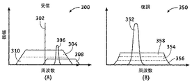
次に図3A〜Bを参照すると、広帯域スペクトラム技術により、従来の単一波長のサンプリング法と比べて改善されたノイズ回避が可能となる。上で説明したように、検知ゾーンが1つの電極112と対応しているか、複数の電極112に共通の変調信号110が提供されて、後の復調および計算のために1つの「電極」として有効に機能する大きな検知ゾーンが生成されうる。変調された波形110は、別個のディジタル符号106の関数であり、印加される検知ゾーンを一意に識別し、これにより、CDMや他の従来の広帯域スペクトラム技術を容易に適用することが可能となる。図3は、キャリア信号111のスペクトル302と、被変調信号110のスペクトル304間の周波数領域の差が強調されている例示的なスペクトルプロット300を示す。単一波長のキャリア信号302と比較して、114で受信される被変調信号の複数周波数スペクトル304は遙かに広い。被変調信号のスペクトル304は非常に広い感受帯域にわたって有効電力が分散しているため、対象となる特定の周波数またはその近傍の狭帯域ノイズ信号306の影響が大幅に低減される。すなわち、単一波長(または狭帯域)のキャリア信号302の近くでスプリアス雑音信号306が仮に発生した場合、検知チャネル113中の電気的効果よりもノイズが支配的となる可能性がある。更に、受信信号116のスペクトルプロット350に示すように、広帯域ノイズ308の悪影響または他の被変調電極チャネル310からの干渉を、広帯域スペクトラム技術によって軽減することができる。プロット350から、被復調信号352(チャネル113の結合および/または被復調検知領域の近くの物体121の存在に対応している)は、比較的狭い周波数帯内に限定されているのに対し、他のチャネルから受信した信号354は、広い帯域に拡散していることがわかる。広帯域のノイズ308と狭帯域のノイズ306のいずれも、被復調信号中で広い周波数帯356および358にわたって同様に拡散している。このため、印加される被変調信号110の帯域幅を上げることによって、被復調信号116の信号対雑音比が劇的に改善される。復調により、信号帯の外のノイズが拡散されて、これが極めて狭くなり、これにより、所望の信号部分352を狭帯域フィルタ等によって容易に抽出できるようになる。この概念は、既知の雑音源を回避するディジタル符号106を選択することによって、更に利用することができる。すなわち、スプリアスノイズの影響を受けやすいことが公知の周波数においてスペクトルの「ギャップ」を形成するために、キャリア信号111に任意のビット長のディジタル符号106が印加される。従来のフーリエ解析を適用する(例えば、単純な高速フーリエ変換(FFT)などを使用する)ことによって、多くの所望のスペクトル特性を有する変調信号110を作成するためのディジタル符号を選択することができる。結果信号116中の、予期されるかまたは実際のノイズを回避するために、被変調電極112に印加される符号が、動作中(例えば図2のステップ210)に変更されても、事前に選択されても、この両方が行われてもよい。別の実施形態では、1つ以上の電極112に印加される特定の符号106が、センサ動作中に、ランダムに、疑似ランダムに、決定論に従って、またはそれ以外の方法で変更されて、経時的に、結果信号116または復調信号118中に存在する任意のノイズが統計学的にフィルタされうる。同様に、特定の空間周波数または空間位置を、(例えば符号化利得によって)強調したり、または異なる変調電極に符号を印加してフィルタ除外することができる。動作中の符号のシフトにより、ノイズの影響または非入力物体(手のひらなど)のスプリアス効果の低減に加えて、ほかの利点(選別または耐湿性など)が提供されうる。各種の同等の実施形態では、ディジタル符号106を変更する代わりに、あるいはこれに加えて、キャリア信号111の周波数、位相、振幅および/または波形が調整されうる。
Referring now to FIGS. 3A-B, wideband spectrum technology allows improved noise avoidance compared to conventional single wavelength sampling methods. As described above, the detection zone corresponds to one electrode 112 or a
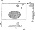
次に図4を参照すると、さまざまな電極112A〜Dに複数の符号化変調信号110A〜Dを同時に印加する広帯域スペクトラム技術により、検知領域101内にある物体121の複数の存在408,410,412を識別することが可能である。例えば、複数の物体は、タッチパッド上の複数本の指、使用中にセンサ100に載っている手のひらの存在や、指とスタイラスが一緒に存在すること、および/またはその他の入力の任意の組合せに対応しうる。複数の存在408,410から生じる電気的効果が、概念的には、図4に示すように、1つ以上の軸404,406上に投影されて、その軸での物体の相対位置が識別されうる。すなわち、電気的効果のピーク値を、検知領域101に対する物体121の相対位置と相関させることができる。図4の例では、「X」軸404および「Y」軸406上に投影された電気的効果の増加によって、指408を識別することができる。ピークの電気的効果の相対X位置およびY位置を相関させることによって、存在408の位置を、二次元(または他の次元数で)で相関させることができる。同様に、図4Aの例は、電気的効果が軸404,406に投影される第2の存在410を示す大きな領域を示している。このような複数の電気的効果の投影を追加で相関させて、領域101に存在する物体121の像(「輪郭」など)を識別することができる。この概念を更に広げると、1つ以上の像408,410がその後適切に処理されうる。領域101の中の複数本の指の存在は、例えば、スクロール、モードの選択または他のタスクを実行するために使用することができる。画像が、ユーザの手のひら(またはその他のユーザの体の不要な部分)から生じたものであると識別することができれば、その画像410を、位置情報または他の出力信号の報告など、後の処理で回避することができる。
Referring now to FIG. 4,
図4に示す例示的な実施形態では、2本の軸404,406は被変調電極112の一部か、または図1Bのように、2つの略直交する方向に配置された、その関連チャネルにほぼ対応している。しかし、別の実施形態では、任意の数の電極112が、重複していたり、重複していなかったり、行列またはその他の構成に配置されてもよい。二次元に配置された、重複する電極112A〜Gを有するセンサ500の例が、図5に示される。このような実施形態では、受信チャネルに対する電気的効果が、2方向の電極のそれぞれの交点で独立して有効に測定され(例えば、X方向とY方向が、等高線プロット400の軸404,406に対応しているなど)、コントローラ102で結果が相関され、404および406のような2つの一次元の「シルエット」ではなく、物体121の二次元の表現または像が提供される。このような場合、第1の方向に配置された電極(例えば電極112A〜C)が、第2の方向に配置された電極(例えば電極112D〜G)とは別の時間に変調され、ある時点での電極のいずれかの組(電極112DとFなど)からの1つ以上の受信信号116が、マルチプレクサ502を介して復調器117に提供される。図5は、さまざまな電極112A〜Gがマルチプレクサ502を介して変調器107と復調器117に結合されていることを示している。また、マルチプレクサは、電極の1つ以上を、復調前に受信回路115に接続しうる。実際には、信号が電極112の一方のサブセットに印加され、もう一方のサブセットで受信されるような任意の方法で、各電極が接続されうる。
In the exemplary embodiment shown in FIG. 4, the two
さまざまな実施形態では、受信チャネルとして機能する2つ以上の電極(例えば、上記のチャネル113に相当する)に、別個の結果信号116が供給されうる。更に、非駆動または不使用の電極(112EおよびGなど)が、電気的基準(グラウンドなど)と結合されるか、または被変調信号によって駆動されて、駆動中の受信チャネルの空間的分解能が改善されうる。この基準は、一般にシールド信号または保護信号と呼ばれており、多重化ロジック502等を介して印加されうる。
In various embodiments, separate result signals 116 may be provided to two or more electrodes that function as receiving channels (eg, corresponding to channel 113 above). In addition, undriven or unused electrodes (such as 112E and G) are coupled to an electrical reference (such as ground) or driven by a modulated signal to improve the spatial resolution of the receiving channel being driven. Can be done. This reference is generally called a shield signal or a protection signal, and can be applied via the
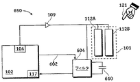
ディジタル符号化処理および他の広帯域スペクトラム技術を、任意の数の異なる方法で機能するセンサにも、同様に適用することができる。図6Aは例示的なセンサ600を示しており、例えば、一次元または多次元に配置された任意の数の被変調電極112A〜Bを備え、これが、被変調電極によって移動された電荷を線形的に変換する容量性フィルタ(積分コンデンサ610など)に結合されている。マイクロコントローラ102/104などが、電極114に結合された112A〜Bを、上で説明したように変調する別個のディジタル符号106を適切に生成する。しかし、この例では、ディジタル符号106は、必ずしも各電極112A〜Bに供給される電圧を符号化するためのものではなく、114に移動される電荷のタイミングを制御するものである。各電極の充電および放電のタイミングを制御し、その後、114から積分コンデンサ610に収集された電荷量を確認することによって、各電極112A〜Bによって提供される電荷量を、被復調信号118から決定することができる。各電極112A〜Bの充電は、受信電極114に電荷を移動すべき場合にのみ各電極に電圧が印加され、それ以外の場合にはフロートとなるようにディジタル符号106を選択することによって制御することができる。個々の電極112A〜Bおよび/またはその組からの電荷を選択的にコンデンサ610に供給することによって、各電極112A〜Bからの結合の量(物体121の近接度によって影響される)を決定することができる。
Digital encoding processes and other wideband spectrum technologies can be applied to sensors that function in any number of different ways as well. FIG. 6A shows an
図6Bは、各電極112で検知と駆動が統合されており、1つ以上のコンデンサ610によってフィルタまたは復調される例示的なセンサを有する別の実施形態を示す。符号106が駆動回路109を変調し、これは電極112に接続された電流源として実装されうる。駆動回路に対する電極の応答が、電極の近くの物体121の結合によって影響され、結果信号(結合によって生じた電圧など)が、回路604およびコンデンサ610によってフィルタおよび/または復調される。フィルタされた信号が更に復調されて、物体の位置属性が決定される。更に、複数の電極が、実質的に直交する符号によって同時に駆動され、復調後に、電極112Aの別の電極112Bへの安定した結合が実質的に相殺されうる。これらの位置検知方法、および他の多くの位置検知方法は、ディジタル符号化処理および広帯域スペクトラムの技術の利益を受ける。
FIG. 6B shows another embodiment with an exemplary sensor that has integrated sensing and driving at each electrode 112 and is filtered or demodulated by one or
次に図7を参照すると、ここに記載の符号化技術に従って形成された各種センサ700が、1つの回路基板または他の基板702に形成されうる。このような実施形態では、検知領域101を形成している電極112A〜Gが基板の一方の面に配置され、処理要素(例えばコントローラ102など)が反対側の面に形成されうる。各種センサ(図1,5に示すセンサ100および500など)では、検知電極、受信電極112,114を互いに物理的に移動させる必要がないため、このようなセンサの電極112,114は、基板702上に任意の方法で堅固に固定されてもよい。基板702は、折りたたみまたは屈曲が可能なように、可撓性材料から形成することができる。更に、安定した絶縁分離を提供し、湿気やごみ、その他の環境的な影響から保護するために、電極上に保護面704が、堆積されるか別の方法によって設けられうる。面704は、ユーザに触覚フィードバックを適切に提供しうる。図8は、可撓性基板802に適切に形成された例示的なセンサ800を示す。図8には、各種の処理要素が、被変調電極および検知電極と基板802の同じ面にあり、基板802が領域101に触覚フィードバックを提供することができることが示されている。さまざまな別の実施形態を作成するために、ここに記載した各種の概念、構造、構成要素および技術が、相互に組み合わされたり、適宜変更されてもよいことを理解すべきである。
Referring now to FIG. 7,
したがって、タッチパッド等の位置検知装置で指、スタイラスまたは他の物体の位置に基づく属性を検出するための数多くのシステム、装置およびプロセスが提供される。上記の詳細な説明において少なくとも1つの代表的な実施形態を示したが、膨大な数の変形例が存在することを理解されたい。例えば、ここに記載される手法のさまざまなステップは、任意の時間的順序において実施されてもよく、ここに提示および/または権利を請求する順序に限定されることはない。また、ここに記載した代表的な実施形態は例に過ぎず、いかなる形であれ本発明の範囲、利用可能性または構成を限定することを意図するものではないことも理解されたい。このため、添付の特許請求の範囲とその法的均等物に記載されている本発明の範囲から逸脱することなく、各種要素の機能および構成をさまざまに変更することができる。 Accordingly, numerous systems, devices and processes are provided for detecting attributes based on the position of a finger, stylus or other object with a position sensing device such as a touchpad. While at least one exemplary embodiment has been presented in the foregoing detailed description, it should be appreciated that a vast number of variations exist. For example, the various steps of the techniques described herein may be performed in any temporal order and are not limited to the order presented and / or claimed herein. It should also be understood that the exemplary embodiments described herein are examples only and are not intended to limit the scope, applicability, or configuration of the invention in any way. Thus, various functions and configurations of the various elements may be made without departing from the scope of the invention as set forth in the appended claims and the legal equivalents thereof.
Claims (10)
前記物体の位置によって電気的に影響された結果信号を前記第2の複数の電極の少なくとも1つにより得るために、前記第1の複数の電極の関連する少なくとも1つに印加される、複数の別個のデジタル符号に基づく複数の変調信号を印加するステップと、
前記複数の別個のデジタル符号を使用して前記結果信号を復調し、前記物体によって引き起こされた電気的効果を選別するステップと、
前記電気的効果から、前記第1及び第2の複数の電極に対する前記物体の前記位置に基づく属性を決定するステップとを含む方法。 A method for detecting an attribute based on a position of an object with respect to the touch sense area in a touch pad device having a touch sense area defined by a first plurality of electrodes and a second plurality of electrodes, comprising:
A plurality of applied to at least one associated one of the first plurality of electrodes to obtain a result signal electrically influenced by the position of the object by at least one of the second plurality of electrodes; Applying a plurality of modulation signals based on separate digital codes;
Demodulating the result signal using the plurality of separate digital codes to screen for electrical effects caused by the object;
Determining an attribute based on the position of the object relative to the first and second plurality of electrodes from the electrical effect.
前記複数の電極のうちの少なくとも一つに関連する前記別個のデジタル符号を用いて前記複数の相補的検出信号のそれぞれを復号し、前記複数の電極から相補的電気的効果を特定するステップと、
前記電気的効果と前記相補的電気的効果とを比較することによって二重差動変換を実行するステップとをさらに含む、請求項1に記載の方法。 The plurality of separate digital codes applied to the associated at least one of the first plurality of electrodes to obtain a plurality of complementary detection signals at the at least one of the second plurality of electrodes. Applying a plurality of complementary modulation signals based on the complement of
Decoding each of the plurality of complementary detection signals using the separate digital code associated with at least one of the plurality of electrodes to identify a complementary electrical effect from the plurality of electrodes;
Further comprising the method of claim 1 and performing a double differential conversion by comparing the complementary electrical effects and the electrical effects.
前記物体の近接度に影響されるように構成された電気的特性を有する複数の電極であって、該複数の電極は、第1方向を持つ第1電極と、前記第1方向とは異なる第2方向を持つ第2電極とを有する複数の電極と、
前記複数の電極の各電極と関連する回路と、
前記複数の電極に関連する復調器と、
前記回路および前記復調器に結合されたプロセッサとを備え、
前記プロセッサは、複数の別個の相互に直交するデジタル符号の関数としての複数の変調信号を生成させ、
前記回路を介して前記第1電極の一又は複数へ前記複数の変調信号をそれぞれ印加させ、
前記物体によって前記複数の電極のうちの少なくとも1つの電極に引き起こされた電気的効果を選別するために、前記デジタル符号を使用して前記第2電極の少なくとも1つから受信した検知信号を復調し、
前記電気的効果から、前記複数の電極に対する前記物体の前記位置に基づく属性を決定するように構成されている、装置。
In a touchpad device for detecting an attribute based on the position of an object,
A plurality of electrodes having electrical characteristics configured to be influenced by proximity of the object, the plurality of electrodes being a first electrode having a first direction and a first electrode different from the first direction; A plurality of electrodes having a second electrode having two directions;
A circuit associated with each electrode of the plurality of electrodes;
A demodulator associated with the plurality of electrodes;
A processor coupled to the circuit and the demodulator,
The processor generates a plurality of modulated signals as a function of a plurality of distinct mutually orthogonal digital codes;
Applying each of the plurality of modulation signals to one or more of the first electrodes via the circuit,
The digital code is used to demodulate a detection signal received from at least one of the second electrodes to screen for electrical effects caused by the object on at least one of the plurality of electrodes. ,
An apparatus configured to determine an attribute based on the position of the object relative to the plurality of electrodes from the electrical effect.
Applications Claiming Priority (3)
| Application Number | Priority Date | Filing Date | Title |
|---|---|---|---|
| US11/274,999 US7868874B2 (en) | 2005-11-15 | 2005-11-15 | Methods and systems for detecting a position-based attribute of an object using digital codes |
| US11/274,999 | 2005-11-15 | ||
| PCT/US2006/040266 WO2007058727A1 (en) | 2005-11-15 | 2006-10-13 | Methods and systems for detecting a position-based attribute of an object using digital codes |
Related Child Applications (1)
| Application Number | Title | Priority Date | Filing Date |
|---|---|---|---|
| JP2013100309A Division JP5512016B2 (en) | 2005-11-15 | 2013-05-10 | Method and system for detecting object position-based attributes using digital codes |
Publications (3)
| Publication Number | Publication Date |
|---|---|
| JP2009516295A JP2009516295A (en) | 2009-04-16 |
| JP2009516295A5 JP2009516295A5 (en) | 2009-11-26 |
| JP5357547B2 true JP5357547B2 (en) | 2013-12-04 |
Family
ID=37768702
Family Applications (2)
| Application Number | Title | Priority Date | Filing Date |
|---|---|---|---|
| JP2008541174A Active JP5357547B2 (en) | 2005-11-15 | 2006-10-13 | Method and system for detecting object position-based attributes using digital codes |
| JP2013100309A Active JP5512016B2 (en) | 2005-11-15 | 2013-05-10 | Method and system for detecting object position-based attributes using digital codes |
Family Applications After (1)
| Application Number | Title | Priority Date | Filing Date |
|---|---|---|---|
| JP2013100309A Active JP5512016B2 (en) | 2005-11-15 | 2013-05-10 | Method and system for detecting object position-based attributes using digital codes |
Country Status (5)
| Country | Link |
|---|---|
| US (9) | US7868874B2 (en) |
| EP (2) | EP1949208B1 (en) |
| JP (2) | JP5357547B2 (en) |
| CN (2) | CN102841704B (en) |
| WO (1) | WO2007058727A1 (en) |
Families Citing this family (358)
| Publication number | Priority date | Publication date | Assignee | Title |
|---|---|---|---|---|
| GB9722766D0 (en) | 1997-10-28 | 1997-12-24 | British Telecomm | Portable computers |
| US7663607B2 (en) | 2004-05-06 | 2010-02-16 | Apple Inc. | Multipoint touchscreen |
| US20040239648A1 (en) | 2003-05-30 | 2004-12-02 | Abdallah David S. | Man-machine interface for controlling access to electronic devices |
| US8643595B2 (en) * | 2004-10-25 | 2014-02-04 | Sipix Imaging, Inc. | Electrophoretic display driving approaches |
| US7868874B2 (en) | 2005-11-15 | 2011-01-11 | Synaptics Incorporated | Methods and systems for detecting a position-based attribute of an object using digital codes |
| US7656168B2 (en) * | 2005-11-28 | 2010-02-02 | Avago Technologies General Ip (Singapore) Pte. Ltd. | Neutralizing electromagnetic noise for a capacitive input device |
| US7657849B2 (en) | 2005-12-23 | 2010-02-02 | Apple Inc. | Unlocking a device by performing gestures on an unlock image |
| US8018440B2 (en) | 2005-12-30 | 2011-09-13 | Microsoft Corporation | Unintentional touch rejection |
| US8144125B2 (en) | 2006-03-30 | 2012-03-27 | Cypress Semiconductor Corporation | Apparatus and method for reducing average scan rate to detect a conductive object on a sensing device |
| US8111243B2 (en) | 2006-03-30 | 2012-02-07 | Cypress Semiconductor Corporation | Apparatus and method for recognizing a tap gesture on a touch sensing device |
| US8279180B2 (en) * | 2006-05-02 | 2012-10-02 | Apple Inc. | Multipoint touch surface controller |
| WO2007146785A2 (en) | 2006-06-09 | 2007-12-21 | Apple Inc. | Touch screen liquid crystal display |
| CN104965621B (en) | 2006-06-09 | 2018-06-12 | 苹果公司 | Touch screen LCD and its operating method |
| US8243027B2 (en) | 2006-06-09 | 2012-08-14 | Apple Inc. | Touch screen liquid crystal display |
| US8059102B2 (en) * | 2006-06-13 | 2011-11-15 | N-Trig Ltd. | Fingertip touch recognition for a digitizer |
| WO2008007372A2 (en) | 2006-07-12 | 2008-01-17 | N-Trig Ltd. | Hover and touch detection for a digitizer |
| US8686964B2 (en) * | 2006-07-13 | 2014-04-01 | N-Trig Ltd. | User specific recognition of intended user interaction with a digitizer |
| US20080074398A1 (en) * | 2006-09-26 | 2008-03-27 | David Gordon Wright | Single-layer capacitive sensing device |
| US7812827B2 (en) | 2007-01-03 | 2010-10-12 | Apple Inc. | Simultaneous sensing arrangement |
| US8493330B2 (en) * | 2007-01-03 | 2013-07-23 | Apple Inc. | Individual channel phase delay scheme |
| US8049732B2 (en) | 2007-01-03 | 2011-11-01 | Apple Inc. | Front-end signal compensation |
| US8094128B2 (en) * | 2007-01-03 | 2012-01-10 | Apple Inc. | Channel scan logic |
| US8711129B2 (en) * | 2007-01-03 | 2014-04-29 | Apple Inc. | Minimizing mismatch during compensation |
| US8125456B2 (en) | 2007-01-03 | 2012-02-28 | Apple Inc. | Multi-touch auto scanning |
| US9710095B2 (en) | 2007-01-05 | 2017-07-18 | Apple Inc. | Touch screen stack-ups |
| US20090225036A1 (en) * | 2007-01-17 | 2009-09-10 | Wright David G | Method and apparatus for discriminating between user interactions |
| US8736420B2 (en) | 2007-01-29 | 2014-05-27 | At&T Intellectual Property I, L.P. | Methods, systems, and products for controlling devices |
| KR101350874B1 (en) * | 2007-02-13 | 2014-01-13 | 삼성디스플레이 주식회사 | Display device and driving method thereof |
| US8243043B2 (en) * | 2007-03-29 | 2012-08-14 | Cirque Corporation | Driven shield for capacitive touchpads |
| US8243013B1 (en) | 2007-05-03 | 2012-08-14 | Sipix Imaging, Inc. | Driving bistable displays |
| US8144126B2 (en) | 2007-05-07 | 2012-03-27 | Cypress Semiconductor Corporation | Reducing sleep current in a capacitance sensing system |
| US20080303780A1 (en) | 2007-06-07 | 2008-12-11 | Sipix Imaging, Inc. | Driving methods and circuit for bi-stable displays |
| US8493331B2 (en) | 2007-06-13 | 2013-07-23 | Apple Inc. | Touch detection using multiple simultaneous frequencies |
| US20090009483A1 (en) * | 2007-06-13 | 2009-01-08 | Apple Inc. | Single-chip touch controller with integrated drive system |
| US8040326B2 (en) * | 2007-06-13 | 2011-10-18 | Apple Inc. | Integrated in-plane switching display and touch sensor |
| US7876311B2 (en) * | 2007-06-13 | 2011-01-25 | Apple Inc. | Detection of low noise frequencies for multiple frequency sensor panel stimulation |
| DK2164365T3 (en) * | 2007-07-04 | 2011-03-14 | Arcelik As | Handles for household appliances |
| DE102007035455A1 (en) * | 2007-07-26 | 2009-02-05 | Diehl Ako Stiftung & Co. Kg | Capacitive touch switch |
| KR20230116073A (en) | 2007-09-24 | 2023-08-03 | 애플 인크. | Embedded authentication systems in an electronic device |
| WO2009049204A1 (en) * | 2007-10-12 | 2009-04-16 | Sipix Imaging, Inc. | Approach to adjust driving waveforms for a display device |
| US8174508B2 (en) * | 2007-11-19 | 2012-05-08 | Microsoft Corporation | Pointing and data entry input device |
| US8600120B2 (en) | 2008-01-03 | 2013-12-03 | Apple Inc. | Personal computing device control using face detection and recognition |
| US10969917B2 (en) * | 2008-01-30 | 2021-04-06 | Apple Inc. | Auto scanning for multiple frequency stimulation multi-touch sensor panels |
| US8319505B1 (en) | 2008-10-24 | 2012-11-27 | Cypress Semiconductor Corporation | Methods and circuits for measuring mutual and self capacitance |
| US20110043478A1 (en) * | 2008-02-27 | 2011-02-24 | Kenichi Matsushima | Proximity detection device and proximity detection method |
| US8358142B2 (en) | 2008-02-27 | 2013-01-22 | Cypress Semiconductor Corporation | Methods and circuits for measuring mutual and self capacitance |
| US8902174B1 (en) * | 2008-02-29 | 2014-12-02 | Cypress Semiconductor Corporation | Resolving multiple presences over a touch sensor array |
| US8462102B2 (en) * | 2008-04-25 | 2013-06-11 | Sipix Imaging, Inc. | Driving methods for bistable displays |
| EP2113827B8 (en) | 2008-04-30 | 2018-09-19 | InnoLux Corporation | Touch input device |
| US20090278794A1 (en) * | 2008-05-09 | 2009-11-12 | Smart Technologies Ulc | Interactive Input System With Controlled Lighting |
| US8228306B2 (en) | 2008-07-23 | 2012-07-24 | Flextronics Ap, Llc | Integration design for capacitive touch panels and liquid crystal displays |
| US9128568B2 (en) | 2008-07-30 | 2015-09-08 | New Vision Display (Shenzhen) Co., Limited | Capacitive touch panel with FPC connector electrically coupled to conductive traces of face-to-face ITO pattern structure in single plane |
| JP5588982B2 (en) * | 2008-08-07 | 2014-09-10 | ラプト アイピー リミテッド | Optical control system with modulated emitter |
| US8390576B2 (en) * | 2008-09-01 | 2013-03-05 | Mediatek, Inc. | Methods and apparatus for detecting user's touch on a touch panel |
| US8207948B2 (en) * | 2008-09-02 | 2012-06-26 | Elan Microelectronics Corporation | Method and systems for identifying objects on a touch-sensitive device |
| US9348451B2 (en) | 2008-09-10 | 2016-05-24 | Apple Inc. | Channel scan architecture for multiple stimulus multi-touch sensor panels |
| US9606663B2 (en) * | 2008-09-10 | 2017-03-28 | Apple Inc. | Multiple stimulation phase determination |
| US8592697B2 (en) | 2008-09-10 | 2013-11-26 | Apple Inc. | Single-chip multi-stimulus sensor controller |
| US8237667B2 (en) | 2008-09-10 | 2012-08-07 | Apple Inc. | Phase compensation for multi-stimulus controller |
| KR100985844B1 (en) * | 2008-10-07 | 2010-10-08 | 주식회사 애트랩 | Portable device with proximity sensor |
| US8558855B2 (en) * | 2008-10-24 | 2013-10-15 | Sipix Imaging, Inc. | Driving methods for electrophoretic displays |
| US9019318B2 (en) * | 2008-10-24 | 2015-04-28 | E Ink California, Llc | Driving methods for electrophoretic displays employing grey level waveforms |
| US8209861B2 (en) | 2008-12-05 | 2012-07-03 | Flextronics Ap, Llc | Method for manufacturing a touch screen sensor assembly |
| US8294047B2 (en) * | 2008-12-08 | 2012-10-23 | Apple Inc. | Selective input signal rejection and modification |
| US8274486B2 (en) | 2008-12-22 | 2012-09-25 | Flextronics Ap, Llc | Diamond pattern on a single layer |
| EP2204726A1 (en) * | 2008-12-30 | 2010-07-07 | STMicroelectronics R&D Oy | Touch screen controller |
| US9251736B2 (en) | 2009-01-30 | 2016-02-02 | E Ink California, Llc | Multiple voltage level driving for electrophoretic displays |
| US20100194733A1 (en) * | 2009-01-30 | 2010-08-05 | Craig Lin | Multiple voltage level driving for electrophoretic displays |
| US20100194789A1 (en) * | 2009-01-30 | 2010-08-05 | Craig Lin | Partial image update for electrophoretic displays |
| US8314779B2 (en) * | 2009-02-23 | 2012-11-20 | Solomon Systech Limited | Method and apparatus for operating a touch panel |
| US20110068810A1 (en) * | 2009-04-03 | 2011-03-24 | Tpo Displays Corp. | Sensing method and driving circuit of capacitive touch screen |
| US8773390B1 (en) * | 2009-04-24 | 2014-07-08 | Cypress Semiconductor Corporation | Biometric identification devices, methods and systems having touch surfaces |
| US9460666B2 (en) | 2009-05-11 | 2016-10-04 | E Ink California, Llc | Driving methods and waveforms for electrophoretic displays |
| US8154529B2 (en) * | 2009-05-14 | 2012-04-10 | Atmel Corporation | Two-dimensional touch sensors |
| US8836648B2 (en) | 2009-05-27 | 2014-09-16 | Microsoft Corporation | Touch pull-in gesture |
| JP5396167B2 (en) * | 2009-06-18 | 2014-01-22 | 株式会社ワコム | Indicator detection apparatus and indicator detection method |
| JP5295008B2 (en) * | 2009-06-18 | 2013-09-18 | 株式会社ワコム | Indicator detection device |
| JP5561513B2 (en) * | 2009-06-23 | 2014-07-30 | トヨタ紡織株式会社 | Capacitance sensor and vehicle proximity sensor using the same |
| WO2011004135A1 (en) | 2009-07-07 | 2011-01-13 | Elliptic Laboratories As | Control using movements |
| US9323398B2 (en) | 2009-07-10 | 2016-04-26 | Apple Inc. | Touch and hover sensing |
| TW201104531A (en) * | 2009-07-17 | 2011-02-01 | Egalax Empia Technology Inc | Method and device for palm rejection |
| US8723827B2 (en) | 2009-07-28 | 2014-05-13 | Cypress Semiconductor Corporation | Predictive touch surface scanning |
| US8384514B2 (en) | 2009-08-07 | 2013-02-26 | At&T Intellectual Property I, L.P. | Enhanced biometric authentication |
| JP5746171B2 (en) * | 2009-08-12 | 2015-07-08 | サーク・コーポレーション | Simultaneous time orthogonal measurement pattern for multiple touch detection on touchpad |
| US8791907B2 (en) * | 2009-08-19 | 2014-07-29 | U-Pixel Technologies Inc. | Touch sensing apparatus and method using different modulated driving signals |
| US20110042153A1 (en) * | 2009-08-19 | 2011-02-24 | U-Pixel Technologies Inc. | Touch sensing device and method using random spread spectrum signal |
| JP5548270B2 (en) * | 2009-08-21 | 2014-07-16 | アップル インコーポレイテッド | Capacitive sensing method and apparatus |
| JP2011047774A (en) * | 2009-08-26 | 2011-03-10 | Seiko Instruments Inc | Proximity detection device and proximity detection method |
| GB2473240A (en) * | 2009-09-04 | 2011-03-09 | Cambridge Display Tech Ltd | A touch screen device using correlated emitter-detector pairs |
| US8269511B2 (en) * | 2009-09-08 | 2012-09-18 | Synaptics Incorporated | Sensing and defining an input object |
| US9036650B2 (en) | 2009-09-11 | 2015-05-19 | Apple Inc. | Automatic low noise frequency selection |
| TWI430168B (en) * | 2009-09-23 | 2014-03-11 | Egalax Empia Technology Inc | Method and device for resistive multi-point touch |
| US9753586B2 (en) | 2009-10-08 | 2017-09-05 | 3M Innovative Properties Company | Multi-touch touch device with multiple drive frequencies and maximum likelihood estimation |
| WO2011041945A1 (en) * | 2009-10-09 | 2011-04-14 | 禾瑞亚科技股份有限公司 | Method and apparatus for analyzing 2 dimension sense information |
| TWI405108B (en) | 2009-10-09 | 2013-08-11 | Egalax Empia Technology Inc | Method and device for analyzing positions |
| US8896548B2 (en) * | 2009-10-09 | 2014-11-25 | Egalax—Empia Technology Inc. | Capacitive touch screen with method and device for converting sensing information including zero cross point |
| CN102063216B (en) | 2009-10-09 | 2012-12-12 | 禾瑞亚科技股份有限公司 | Device and method for parallel-scanning differential touch detection |
| EP2503432A4 (en) | 2009-10-09 | 2014-07-23 | Egalax Empia Technology Inc | Method and device for dual-differential sensing |
| US8576164B2 (en) | 2009-10-26 | 2013-11-05 | Sipix Imaging, Inc. | Spatially combined waveforms for electrophoretic displays |
| JP5341719B2 (en) * | 2009-11-12 | 2013-11-13 | 京セラ株式会社 | Mobile communication terminal and input control program |
| US8535133B2 (en) * | 2009-11-16 | 2013-09-17 | Broadcom Corporation | Video game with controller sensing player inappropriate activity |
| US8558802B2 (en) * | 2009-11-21 | 2013-10-15 | Freescale Semiconductor, Inc. | Methods and apparatus for performing capacitive touch sensing and proximity detection |
| JP5295090B2 (en) * | 2009-12-18 | 2013-09-18 | 株式会社ワコム | Indicator detection device |
| US20120327010A1 (en) * | 2009-12-21 | 2012-12-27 | Soft Haptic Technology Inc. | Pointing device |
| NO20093601A1 (en) | 2009-12-29 | 2011-06-30 | Idex Asa | surface Sensor |
| US8866347B2 (en) | 2010-01-15 | 2014-10-21 | Idex Asa | Biometric image sensing |
| US8421890B2 (en) | 2010-01-15 | 2013-04-16 | Picofield Technologies, Inc. | Electronic imager using an impedance sensor grid array and method of making |
| US11049463B2 (en) * | 2010-01-15 | 2021-06-29 | E Ink California, Llc | Driving methods with variable frame time |
| US8791792B2 (en) * | 2010-01-15 | 2014-07-29 | Idex Asa | Electronic imager using an impedance sensor grid array mounted on or about a switch and method of making |
| US8558786B2 (en) * | 2010-01-20 | 2013-10-15 | Sipix Imaging, Inc. | Driving methods for electrophoretic displays |
| US20110185320A1 (en) * | 2010-01-28 | 2011-07-28 | Microsoft Corporation | Cross-reference Gestures |
| US20110185299A1 (en) * | 2010-01-28 | 2011-07-28 | Microsoft Corporation | Stamp Gestures |
| US9411504B2 (en) | 2010-01-28 | 2016-08-09 | Microsoft Technology Licensing, Llc | Copy and staple gestures |
| US8261213B2 (en) | 2010-01-28 | 2012-09-04 | Microsoft Corporation | Brush, carbon-copy, and fill gestures |
| US9519356B2 (en) * | 2010-02-04 | 2016-12-13 | Microsoft Technology Licensing, Llc | Link gestures |
| US20110191704A1 (en) * | 2010-02-04 | 2011-08-04 | Microsoft Corporation | Contextual multiplexing gestures |
| US9310994B2 (en) * | 2010-02-19 | 2016-04-12 | Microsoft Technology Licensing, Llc | Use of bezel as an input mechanism |
| US8799827B2 (en) * | 2010-02-19 | 2014-08-05 | Microsoft Corporation | Page manipulations using on and off-screen gestures |
| US9965165B2 (en) * | 2010-02-19 | 2018-05-08 | Microsoft Technology Licensing, Llc | Multi-finger gestures |
| US9367205B2 (en) | 2010-02-19 | 2016-06-14 | Microsoft Technolgoy Licensing, Llc | Radial menus with bezel gestures |
| US9274682B2 (en) | 2010-02-19 | 2016-03-01 | Microsoft Technology Licensing, Llc | Off-screen gestures to create on-screen input |
| US20110209058A1 (en) * | 2010-02-25 | 2011-08-25 | Microsoft Corporation | Multi-screen hold and tap gesture |
| US9075522B2 (en) * | 2010-02-25 | 2015-07-07 | Microsoft Technology Licensing, Llc | Multi-screen bookmark hold gesture |
| US20110209089A1 (en) * | 2010-02-25 | 2011-08-25 | Hinckley Kenneth P | Multi-screen object-hold and page-change gesture |
| US9454304B2 (en) * | 2010-02-25 | 2016-09-27 | Microsoft Technology Licensing, Llc | Multi-screen dual tap gesture |
| CN101847069B (en) * | 2010-03-03 | 2012-07-04 | 敦泰科技(深圳)有限公司 | Multi-point touch detection method of touch screen |
| US9224338B2 (en) * | 2010-03-08 | 2015-12-29 | E Ink California, Llc | Driving methods for electrophoretic displays |
| JP5429814B2 (en) * | 2010-03-29 | 2014-02-26 | 株式会社ワコム | Indicator detection device and detection sensor |
| US9285929B2 (en) | 2010-03-30 | 2016-03-15 | New Vision Display (Shenzhen) Co., Limited | Touchscreen system with simplified mechanical touchscreen design using capacitance and acoustic sensing technologies, and method therefor |
| US8766930B2 (en) * | 2010-06-02 | 2014-07-01 | Pixart Imaging Inc. | Capacitive touchscreen system with drive-sense circuits |
| US8692781B2 (en) * | 2010-06-02 | 2014-04-08 | Pixart Imaging Inc. | Capacitive touchscreen system with multiplexers |
| US9013394B2 (en) | 2010-06-04 | 2015-04-21 | E Ink California, Llc | Driving method for electrophoretic displays |
| US9551738B2 (en) | 2010-06-08 | 2017-01-24 | Iee International Electronics & Engineering S.A. | Robust capacitive measurement system |
| WO2011154468A1 (en) | 2010-06-08 | 2011-12-15 | Iee International Electronics & Engineering S.A. | Robust capacitive measurement system |
| TWI403948B (en) * | 2010-06-08 | 2013-08-01 | Au Optronics Corp | Method of reducing noises on a touch panel |
| US8988080B2 (en) * | 2010-06-08 | 2015-03-24 | Iee International Electronics & Engineering S.A. | Capacitive measurement system with increased robustness against electro-magnetic interference |
| KR101431366B1 (en) * | 2010-07-20 | 2014-08-19 | 엠파이어 테크놀로지 디벨롭먼트 엘엘씨 | Augmented reality proximity sensing |
| US8528072B2 (en) | 2010-07-23 | 2013-09-03 | Apple Inc. | Method, apparatus and system for access mode control of a device |
| KR101710657B1 (en) | 2010-08-05 | 2017-02-28 | 삼성디스플레이 주식회사 | Display device and driving method thereof |
| US9098138B2 (en) | 2010-08-27 | 2015-08-04 | Apple Inc. | Concurrent signal detection for touch and hover sensing |
| US8730204B2 (en) * | 2010-09-16 | 2014-05-20 | Synaptics Incorporated | Systems and methods for signaling and interference detection in sensor devices |
| WO2012050561A1 (en) * | 2010-10-11 | 2012-04-19 | Hewlett-Packard Development Company, L.P. | A first image and a second image on a display |
| EP2455840A1 (en) * | 2010-11-02 | 2012-05-23 | Sony Ericsson Mobile Communications AB | Communication device and method |
| TWI441065B (en) * | 2010-11-03 | 2014-06-11 | Elan Microelectronics Corp | A Capacitive Touch Element for Identifying Conductor and Non - Conductor and Its Method of Discrimination |
| CN102455815B (en) * | 2010-11-03 | 2015-04-22 | 矽统科技股份有限公司 | Touch sensing device and method thereof |
| TWI598672B (en) | 2010-11-11 | 2017-09-11 | 希畢克斯幻像有限公司 | Driving method for electrophoretic displays |
| JP4927216B1 (en) | 2010-11-12 | 2012-05-09 | シャープ株式会社 | Linear element array value estimation method, capacitance detection method, integrated circuit, touch sensor system, and electronic device |
| JP5578566B2 (en) * | 2010-12-08 | 2014-08-27 | 株式会社ワコム | Indicator detection apparatus and indicator detection method |
| US8804056B2 (en) | 2010-12-22 | 2014-08-12 | Apple Inc. | Integrated touch screens |
| CN102063206A (en) * | 2010-12-31 | 2011-05-18 | 黄天麒 | Photoelectronic input device |
| TWI403939B (en) * | 2010-12-31 | 2013-08-01 | Au Optronics Corp | Touch panel and touch display panel |
| KR101773612B1 (en) * | 2011-01-13 | 2017-08-31 | 삼성전자주식회사 | Apparatus for determining touch position and method for the same |
| CN102707821B (en) * | 2011-03-28 | 2015-04-22 | 深圳市汇顶科技股份有限公司 | Method and system for de-noising touch detection device |
| US10198097B2 (en) | 2011-04-26 | 2019-02-05 | Sentons Inc. | Detecting touch input force |
| US9639213B2 (en) | 2011-04-26 | 2017-05-02 | Sentons Inc. | Using multiple signals to detect touch input |
| CN103608749B (en) * | 2011-04-26 | 2016-12-07 | 加利福尼亚大学董事会 | The system felt for record and reproduction and device |
| US9477350B2 (en) * | 2011-04-26 | 2016-10-25 | Sentons Inc. | Method and apparatus for active ultrasonic touch devices |
| US9189109B2 (en) | 2012-07-18 | 2015-11-17 | Sentons Inc. | Detection of type of object used to provide a touch contact input |
| US11327599B2 (en) | 2011-04-26 | 2022-05-10 | Sentons Inc. | Identifying a contact type |
| JP5615235B2 (en) * | 2011-06-20 | 2014-10-29 | アルプス電気株式会社 | Coordinate detection apparatus and coordinate detection program |
| JP5539269B2 (en) * | 2011-06-27 | 2014-07-02 | シャープ株式会社 | Capacitance value distribution detection method, capacitance value distribution detection circuit, touch sensor system, and information input / output device |
| WO2012176639A1 (en) | 2011-06-22 | 2012-12-27 | Sharp Kabushiki Kaisha | Touch panel system and electronic device |
| US8976154B2 (en) * | 2011-06-22 | 2015-03-10 | Sharp Kabushiki Kaisha | Touch panel system and electronic device |
| JP5384598B2 (en) | 2011-09-09 | 2014-01-08 | シャープ株式会社 | Capacitive touch sensor panel, capacitive touch sensor system using the same, and information input / output device |
| TWI499957B (en) | 2011-06-22 | 2015-09-11 | Sharp Kk | Touch panel system and electronic device |
| JP5350437B2 (en) | 2011-06-27 | 2013-11-27 | シャープ株式会社 | Touch sensor system |
| US8743080B2 (en) | 2011-06-27 | 2014-06-03 | Synaptics Incorporated | System and method for signaling in sensor devices |
| US9830026B2 (en) | 2011-06-29 | 2017-11-28 | Sharp Kabushiki Kaisha | Touch sensor system and electronic device |
| US8752200B2 (en) | 2011-07-12 | 2014-06-10 | At&T Intellectual Property I, L.P. | Devices, systems and methods for security using magnetic field based identification |
| US20130038378A1 (en) * | 2011-08-12 | 2013-02-14 | Tajeshwar Singh | Touch Sensing With A Common Driver |
| US20130037330A1 (en) * | 2011-08-12 | 2013-02-14 | Tajeshwar Singh | Touch Sensing With A Common Driver |
| US9002322B2 (en) | 2011-09-29 | 2015-04-07 | Apple Inc. | Authentication with secondary approver |
| US8769624B2 (en) | 2011-09-29 | 2014-07-01 | Apple Inc. | Access control utilizing indirect authentication |
| US10235004B1 (en) | 2011-11-18 | 2019-03-19 | Sentons Inc. | Touch input detector with an integrated antenna |
| US11262253B2 (en) | 2017-08-14 | 2022-03-01 | Sentons Inc. | Touch input detection using a piezoresistive sensor |
| EP2780783B1 (en) | 2011-11-18 | 2022-12-28 | Sentons Inc. | Detecting touch input force |
| US9176621B2 (en) * | 2011-11-18 | 2015-11-03 | Synaptics Incorporated | Flexible timing and multiplexing for a display device comprising an integrated capacitive sensing device |
| KR101852549B1 (en) | 2011-11-18 | 2018-04-27 | 센톤스 아이엔씨. | Localized haptic feedback |
| KR101398322B1 (en) * | 2011-12-05 | 2014-05-23 | 엘지디스플레이 주식회사 | Sensing device and method for touch screen |
| TWI447631B (en) * | 2011-12-07 | 2014-08-01 | Ind Tech Res Inst | Projective capacitance touch apparatus and touching control method thereof |
| KR101339490B1 (en) * | 2011-12-14 | 2013-12-10 | 삼성전기주식회사 | Apparatus and method for sensing touch input |
| CN108459757B (en) * | 2011-12-19 | 2022-04-01 | 禾瑞亚科技股份有限公司 | Processor and touch control method of touch screen |
| US8766949B2 (en) | 2011-12-22 | 2014-07-01 | Synaptics Incorporated | Systems and methods for determining user input using simultaneous transmission from multiple electrodes |
| US8525955B2 (en) | 2012-01-31 | 2013-09-03 | Multek Display (Hong Kong) Limited | Heater for liquid crystal display |
| GB2499242A (en) * | 2012-02-10 | 2013-08-14 | Alterix Ltd | methods of operating excitation circuitry and/or measurement circuitry in a digitiser and a method of manufacturing a transducer for a digitiser |
| JP5960293B2 (en) * | 2012-02-27 | 2016-08-02 | 熊光 蔡 | Display device and touch detection method thereof |
| US20150002452A1 (en) * | 2012-03-15 | 2015-01-01 | Sony Mobile Communications Ab | Method for controlling a touch sensor |
| EP2958053A1 (en) | 2012-04-10 | 2015-12-23 | Idex Asa | Biometric sensing |
| US9086768B2 (en) | 2012-04-30 | 2015-07-21 | Apple Inc. | Mitigation of parasitic capacitance |
| US9201547B2 (en) | 2012-04-30 | 2015-12-01 | Apple Inc. | Wide dynamic range capacitive sensing |
| AU2013262488A1 (en) | 2012-05-18 | 2014-12-18 | Apple Inc. | Device, method, and graphical user interface for manipulating user interfaces based on fingerprint sensor inputs |
| US8970544B1 (en) * | 2012-05-24 | 2015-03-03 | Maxim Integrated Products, Inc. | Digital filtering and spread spectrum based interference mitigation for mutual and self capacitance panel |
| US8982091B1 (en) * | 2012-05-24 | 2015-03-17 | Maxim Integrated Products, Inc. | Hadamard matrix based projected mutual capacitance touch panel decoding |
| US9235280B1 (en) * | 2012-05-24 | 2016-01-12 | Qualcomm Technologies, Inc. | Mutual capacitance large panel phase shift mitigation |
| TW201350974A (en) * | 2012-06-08 | 2013-12-16 | Inv Element Inc | In-cell touch display panel system with increased accuracy of touch positions |
| US9063608B2 (en) | 2012-06-14 | 2015-06-23 | Synaptics Incorporated | Systems and methods for sensor devices having a non-commensurate number of transmitter electrodes |
| TWI470491B (en) | 2012-06-19 | 2015-01-21 | Ind Tech Res Inst | Feedback tactile sense apparatus |
| CN103543855A (en) * | 2012-07-10 | 2014-01-29 | 程芹 | Touch screen system and method for positioning touch coordinates |
| US9348468B2 (en) | 2013-06-07 | 2016-05-24 | Sentons Inc. | Detecting multi-touch inputs |
| US9654184B2 (en) * | 2012-07-20 | 2017-05-16 | WIPQTUS Inc. | Transmitter to receiver communication link in a wireless power system |
| US9176604B2 (en) * | 2012-07-27 | 2015-11-03 | Apple Inc. | Stylus device |
| US9958966B2 (en) | 2012-10-16 | 2018-05-01 | Atmel Corporation | Active stylus communication and position system |
| US9841862B2 (en) | 2012-10-16 | 2017-12-12 | Atmel Corporation | Stylus position system |
| US10013096B2 (en) * | 2012-10-18 | 2018-07-03 | Atmel Corporation | Touch sensor with simultaneously driven drive electrodes |
| JP6340373B2 (en) | 2012-11-06 | 2018-06-06 | ニューポート・コーポレイションNewport Corporation | Capacitive load presence and type detection system |
| TWI507952B (en) * | 2012-11-08 | 2015-11-11 | Mstar Semiconductor Inc | Touch control system and capacitance detecting apparatus thereof |
| US8928615B2 (en) * | 2012-11-08 | 2015-01-06 | Good Will Instrument Co., Ltd. | Oscilloscope with touch control and touch control operating method of displaying waveform thereof |
| US9582122B2 (en) | 2012-11-12 | 2017-02-28 | Microsoft Technology Licensing, Llc | Touch-sensitive bezel techniques |
| WO2014081104A1 (en) * | 2012-11-21 | 2014-05-30 | Lg Electronics Inc. | Multimedia device for having touch sensor and method for controlling the same |
| CN103837748B (en) * | 2012-11-23 | 2017-06-16 | 晨星软件研发(深圳)有限公司 | Touch-control system and its electric capacity amount detecting device |
| US20140204053A1 (en) * | 2013-01-22 | 2014-07-24 | Pixart Imaging Inc. | Concurrent driving capacitive touch sensing device and transmission system |
| US9075465B2 (en) * | 2013-02-19 | 2015-07-07 | Himax Technologies Limited | Method of identifying touch event on touch panel by shape of signal group and computer readable medium thereof |
| WO2014145872A1 (en) * | 2013-03-15 | 2014-09-18 | Tactual Labs Co. | Fast multi-touch stylus and sensor |
| US20140267143A1 (en) * | 2013-03-15 | 2014-09-18 | Synaptics Incorporated | System and method for a transcapacitive proximity sensing device |
| MX349679B (en) * | 2013-03-15 | 2017-08-09 | Tactual Labs Co | Fast multi-touch sensor with user identification techniques. |
| BR112015022961A2 (en) * | 2013-03-15 | 2017-07-18 | Tactual Labs Co | fast multitap noise reduction |
| US9019224B2 (en) * | 2013-03-15 | 2015-04-28 | Tactual Labs Co. | Low-latency touch sensitive device |
| KR102011433B1 (en) * | 2013-04-22 | 2019-10-22 | 삼성디스플레이 주식회사 | Touch Sensing Apparatus and Touch Sensing Method Using the Same |
| JP5902351B2 (en) * | 2013-05-10 | 2016-04-13 | シャープ株式会社 | Touch panel system, stylus pen, and electronic device |
| US9658728B2 (en) * | 2013-06-20 | 2017-05-23 | Sharp Kabushiki Kaisha | Touch panel controller, integrated circuit, touch panel device, and electronic device |
| US8988390B1 (en) | 2013-07-03 | 2015-03-24 | Apple Inc. | Frequency agile touch processing |
| KR101438636B1 (en) * | 2013-07-25 | 2014-09-05 | 현대자동차 주식회사 | Touch point recognition method of touch screen and the system performing this |
| US9619090B2 (en) | 2013-07-29 | 2017-04-11 | Microsoft Technology Licensing, Llc | Finger touch sensing with a digitizer system |
| KR20150017123A (en) * | 2013-08-06 | 2015-02-16 | 삼성디스플레이 주식회사 | Touch sensor and drinving method thereof |
| US9542023B2 (en) | 2013-08-07 | 2017-01-10 | Synaptics Incorporated | Capacitive sensing using matrix electrodes driven by routing traces disposed in a source line layer |
| US10042446B2 (en) | 2013-08-13 | 2018-08-07 | Samsung Electronics Company, Ltd. | Interaction modes for object-device interactions |
| US10108305B2 (en) * | 2013-08-13 | 2018-10-23 | Samsung Electronics Company, Ltd. | Interaction sensing |
| US10141929B2 (en) | 2013-08-13 | 2018-11-27 | Samsung Electronics Company, Ltd. | Processing electromagnetic interference signal using machine learning |
| US10073578B2 (en) | 2013-08-13 | 2018-09-11 | Samsung Electronics Company, Ltd | Electromagnetic interference signal detection |
| US10101869B2 (en) | 2013-08-13 | 2018-10-16 | Samsung Electronics Company, Ltd. | Identifying device associated with touch event |
| KR102111032B1 (en) | 2013-08-14 | 2020-05-15 | 삼성디스플레이 주식회사 | Touch sensing display device |
| US9569054B2 (en) | 2013-08-19 | 2017-02-14 | Touchsensor Technologies, Llc | Capacitive sensor filtering apparatus, method, and system |
| US10013113B2 (en) | 2013-08-19 | 2018-07-03 | Touchsensor Technologies, Llc | Capacitive sensor filtering apparatus, method, and system |
| US9430111B2 (en) | 2013-08-19 | 2016-08-30 | Touchsensor Technologies, Llc | Capacitive sensor filtering apparatus, method, and system |
| US9898642B2 (en) | 2013-09-09 | 2018-02-20 | Apple Inc. | Device, method, and graphical user interface for manipulating user interfaces based on fingerprint sensor inputs |
| US9588552B2 (en) * | 2013-09-11 | 2017-03-07 | Sentons Inc. | Attaching electrical components using non-conductive adhesive |
| US9459715B1 (en) | 2013-09-20 | 2016-10-04 | Sentons Inc. | Using spectral control in detecting touch input |
| CN104516555A (en) * | 2013-09-27 | 2015-04-15 | 天津富纳源创科技有限公司 | Method for preventing error touch of touch panel |
| US9430097B2 (en) | 2013-09-30 | 2016-08-30 | Synaptics Incorporated | Non-orthogonal coding techniques for optical sensing |
| US10726760B2 (en) | 2013-10-07 | 2020-07-28 | E Ink California, Llc | Driving methods to produce a mixed color state for an electrophoretic display |
| TWI550332B (en) | 2013-10-07 | 2016-09-21 | 電子墨水加利福尼亞有限責任公司 | Driving methods for color display device |
| US10380931B2 (en) | 2013-10-07 | 2019-08-13 | E Ink California, Llc | Driving methods for color display device |
| US9274662B2 (en) | 2013-10-18 | 2016-03-01 | Synaptics Incorporated | Sensor matrix pad for performing multiple capacitive sensing techniques |
| KR102140197B1 (en) * | 2013-10-23 | 2020-08-03 | 삼성디스플레이 주식회사 | Capacitive type touch sensor |
| TWI505165B (en) * | 2013-11-15 | 2015-10-21 | Ili Technology Corp | Touch sensor and operating method thereof |
| US9933879B2 (en) | 2013-11-25 | 2018-04-03 | Apple Inc. | Reconfigurable circuit topology for both self-capacitance and mutual capacitance sensing |
| CN116560524A (en) | 2013-12-13 | 2023-08-08 | 苹果公司 | Integrated touch and display architecture for self-capacitance touch sensor |
| EP3079043A4 (en) * | 2014-01-26 | 2017-01-18 | Huawei Device Co., Ltd. | Interference suppression method and apparatus for touch screen and terminal device |
| KR101606404B1 (en) * | 2014-03-05 | 2016-03-25 | 주식회사 동부하이텍 | A touch sensor |
| US10372232B2 (en) * | 2014-03-12 | 2019-08-06 | Hewlett-Packard Development Company, L.P. | Keyboard devices with flexible layers and lattice substrates |
| US9477337B2 (en) | 2014-03-14 | 2016-10-25 | Microsoft Technology Licensing, Llc | Conductive trace routing for display and bezel sensors |
| US9176633B2 (en) | 2014-03-31 | 2015-11-03 | Synaptics Incorporated | Sensor device and method for estimating noise in a capacitive sensing device |
| US10042483B2 (en) * | 2014-04-18 | 2018-08-07 | Atmel Corporation | Touch system with code hopping algorithms and code division multiplexing |
| WO2015166568A1 (en) * | 2014-04-30 | 2015-11-05 | 楽天株式会社 | Input device, input method, and program |
| WO2015178920A1 (en) | 2014-05-22 | 2015-11-26 | Onamp Research Llc | Panel bootstrapping architectures for in-cell self-capacitance |
| US10043185B2 (en) | 2014-05-29 | 2018-08-07 | Apple Inc. | User interface for payments |
| JP2015230599A (en) | 2014-06-05 | 2015-12-21 | 株式会社ジャパンディスプレイ | Display device with sensor and its drive method |
| US9304643B2 (en) * | 2014-06-24 | 2016-04-05 | Synaptics Incorporated | Classifying input objects interacting with a capacitive button |
| KR102161745B1 (en) * | 2014-07-01 | 2020-10-06 | 삼성디스플레이 주식회사 | Accelerator for providing visual feedback to touch input, touch input processing device and method for providing visual feedback to touch input |
| KR101630047B1 (en) * | 2014-07-08 | 2016-06-14 | 한양대학교 산학협력단 | Appratus of Capacitive Touch Panel and Method of driving the same |
| US20160034080A1 (en) * | 2014-08-01 | 2016-02-04 | Jin-chul Lee | Semiconductor device and method of operating the same |
| KR102249203B1 (en) | 2014-09-05 | 2021-05-10 | 삼성전자주식회사 | Coordinate indicating apparatus and method for driving thereof |
| TWI559202B (en) * | 2014-10-01 | 2016-11-21 | 義隆電子股份有限公司 | Capacitive touch device and exciting signal generating circuit and method thereof |
| US9804719B2 (en) * | 2014-10-23 | 2017-10-31 | Semiconductor Energy Laboratory Co., Ltd. | Electronic device |
| KR102249736B1 (en) * | 2014-10-27 | 2021-05-10 | 삼성전자주식회사 | sensor panel driving method and electronic device supporting the same |
| CN104461194A (en) * | 2014-10-29 | 2015-03-25 | 张明 | Spread spectrum capacitance type touch sensor |
| CN104461193A (en) * | 2014-10-29 | 2015-03-25 | 张明 | Method for increasing signal-to-noise ratio of capacitive touch sensor |
| US9542588B2 (en) * | 2014-11-17 | 2017-01-10 | Cypress Semiconductor Corporations | Capacitive fingerprint sensor with quadrature demodulator and multiphase scanning |
| WO2016079776A1 (en) * | 2014-11-17 | 2016-05-26 | 株式会社ワコム | Position indicator |
| KR101628894B1 (en) * | 2014-12-09 | 2016-06-14 | 한승희 | Touch sensing method, touch sensing controller and touch sensing device |
| US11402945B2 (en) | 2014-12-09 | 2022-08-02 | Seung-Hee Han | Touch sensing method and touch sensing device based on driving and sensing signals |
| US9952732B2 (en) | 2014-12-10 | 2018-04-24 | Pixart Imaging Inc. | Capacitive touch device, capacitive communication device and communication system |
| US9800292B2 (en) | 2014-12-10 | 2017-10-24 | Pixart Imaging Inc | Capacitive communication system and Bluetooth pairing method |
| US10452195B2 (en) | 2014-12-30 | 2019-10-22 | Samsung Electronics Co., Ltd. | Electronic system with gesture calibration mechanism and method of operation thereof |
| US9778713B2 (en) | 2015-01-05 | 2017-10-03 | Synaptics Incorporated | Modulating a reference voltage to preform capacitive sensing |
| KR102276911B1 (en) | 2015-01-14 | 2021-07-13 | 삼성전자주식회사 | Touch controller, touch sensing device and touch sensing method |
| CN107209602B (en) | 2015-02-02 | 2020-05-26 | 苹果公司 | Flexible self-capacitance and mutual capacitance touch sensing system architecture |
| CN107250818B (en) * | 2015-03-06 | 2020-03-17 | 德州仪器公司 | Broadband capacitive sensing using sensing signal modulation |
| KR102109419B1 (en) * | 2015-03-09 | 2020-05-12 | 주식회사 디비하이텍 | A touch sensor |
| KR102319276B1 (en) * | 2015-03-09 | 2021-11-01 | 주식회사 디비하이텍 | A touch sensor |
| US10095361B2 (en) | 2015-03-18 | 2018-10-09 | Microsoft Technology Licensing, Llc | Stylus detection with capacitive based digitizer sensor |
| US9874966B2 (en) | 2015-04-28 | 2018-01-23 | Microsoft Technology Licensing, Llc | Electrostatic device having spaced electrodes |
| USD776664S1 (en) * | 2015-05-20 | 2017-01-17 | Chaya Coleena Hendrick | Smart card |
| US9778804B2 (en) * | 2015-06-04 | 2017-10-03 | Synaptics Incorporated | Calibrating charge mismatch in a baseline correction circuit |
| US9720541B2 (en) | 2015-06-30 | 2017-08-01 | Synaptics Incorporated | Arrangement of sensor pads and display driver pads for input device |
| US9715304B2 (en) | 2015-06-30 | 2017-07-25 | Synaptics Incorporated | Regular via pattern for sensor-based input device |
| KR20170029377A (en) | 2015-09-07 | 2017-03-15 | 삼성전자주식회사 | Oordinate indicating apparatus and method for sensing of hover |
| US10380397B2 (en) | 2015-09-09 | 2019-08-13 | Cypress Semiconductor Corporation | Half-bridge fingeprint sensing method |
| US10013593B2 (en) | 2015-09-09 | 2018-07-03 | Cypress Semiconductor Corporation | Multiphase fingerprint sensor layout and construction |
| US10048811B2 (en) | 2015-09-18 | 2018-08-14 | Sentons Inc. | Detecting touch input provided by signal transmitting stylus |
| US10025428B2 (en) | 2015-11-19 | 2018-07-17 | Synaptics Incorporated | Method and apparatus for improving capacitive sensing detection |
| DE102015226129A1 (en) | 2015-12-21 | 2017-06-22 | Robert Bosch Gmbh | Method for operating a sensor system, sensor element and sensor system |
| US10423268B2 (en) | 2015-12-22 | 2019-09-24 | Microsoft Technology Licensing, Llc | System and method for detecting grounding state of a touch enabled computing device |
| US10296146B2 (en) | 2015-12-22 | 2019-05-21 | Microsoft Technology Licensing, Llc | System and method for detecting grip of a touch enabled device |
| US10067587B2 (en) | 2015-12-29 | 2018-09-04 | Synaptics Incorporated | Routing conductors in an integrated display device and sensing device |
| CN106775046B (en) * | 2015-12-31 | 2020-02-11 | 深圳市汇顶科技股份有限公司 | Same-frequency noise processing method, same-frequency noise processing device and same-frequency noise processing system |
| US9823774B2 (en) | 2016-02-23 | 2017-11-21 | Microsoft Technology Licensing, Llc | Noise reduction in a digitizer system |
| CN112416149A (en) * | 2016-03-08 | 2021-02-26 | 禾瑞亚科技股份有限公司 | Touch control device for detecting inclination angle of touch pen and control method thereof |
| US10019122B2 (en) | 2016-03-31 | 2018-07-10 | Synaptics Incorporated | Capacitive sensing using non-integer excitation |
| JP6557628B2 (en) | 2016-03-31 | 2019-08-07 | 株式会社ジャパンディスプレイ | Detection device, display device, and detection method |
| US10004048B2 (en) * | 2016-04-01 | 2018-06-19 | Intel Corporation | Transmission power control methods and devices |
| DK179186B1 (en) | 2016-05-19 | 2018-01-15 | Apple Inc | REMOTE AUTHORIZATION TO CONTINUE WITH AN ACTION |
| US20170371487A1 (en) * | 2016-06-28 | 2017-12-28 | Tactual Labs Co. | Frame-phase synchronization in frequency division modulated touch systems |
| KR102287074B1 (en) * | 2016-07-29 | 2021-08-06 | 애플 인크. | Touch sensor panel with multi-power domain chip configuration |
| KR20180015025A (en) | 2016-08-02 | 2018-02-12 | 삼성전자주식회사 | Analog front end for read-out signals from on-display fingerprint sensor and device having the same |
| KR102635898B1 (en) * | 2016-10-25 | 2024-02-15 | 엘지디스플레이 주식회사 | Finger sensor integrated type touch screen device |
| JP2018072928A (en) | 2016-10-25 | 2018-05-10 | シナプティクス インコーポレイテッド | Sensing system, touch detection circuit and semiconductor device |
| US10261604B2 (en) | 2016-11-04 | 2019-04-16 | Microsoft Technology Licensing, Llc | Active stylus velocity correction |
| US10126874B2 (en) | 2016-11-08 | 2018-11-13 | Synaptics Incorporated | Active pen panel receiver interference cancellation |
| US10908741B2 (en) | 2016-11-10 | 2021-02-02 | Sentons Inc. | Touch input detection along device sidewall |
| US10296144B2 (en) | 2016-12-12 | 2019-05-21 | Sentons Inc. | Touch input detection with shared receivers |
| CN108228250A (en) * | 2016-12-19 | 2018-06-29 | 南昌欧菲生物识别技术有限公司 | The display methods and terminal of a kind of application interface |
| TWI613636B (en) * | 2016-12-28 | 2018-02-01 | 財團法人工業技術研究院 | Driving device and driving method |
| CN108256399B (en) * | 2016-12-28 | 2020-10-27 | 上海箩箕技术有限公司 | Fingerprint imaging module and electronic equipment |
| US10528180B2 (en) * | 2016-12-30 | 2020-01-07 | Cirque Corporation | Waterproof touch keypad with skimmer detection |
| US10126877B1 (en) | 2017-02-01 | 2018-11-13 | Sentons Inc. | Update of reference data for touch input detection |
| CN108399356A (en) * | 2017-02-08 | 2018-08-14 | 茂丞科技股份有限公司 | Fingerprint acquisition apparatus and fingerprinting method |
| US10585522B2 (en) | 2017-02-27 | 2020-03-10 | Sentons Inc. | Detection of non-touch inputs using a signature |
| US10338742B2 (en) * | 2017-03-02 | 2019-07-02 | Microsoft Technology Licensing, Llc | Detection method for a digitizer |
| EP3407172B1 (en) * | 2017-03-16 | 2022-01-12 | Shenzhen Goodix Technology Co., Ltd. | Touch detection method and system |
| US10089514B1 (en) | 2017-03-31 | 2018-10-02 | Synaptics Incorporated | Adaptive reference for differential capacitive measurements |
| JP2018190095A (en) * | 2017-04-28 | 2018-11-29 | 株式会社ジャパンディスプレイ | Detection device, display device and detection method |
| US11580829B2 (en) | 2017-08-14 | 2023-02-14 | Sentons Inc. | Dynamic feedback for haptics |
| US10466848B2 (en) * | 2017-08-28 | 2019-11-05 | Synaptics Incorporated | CDM excitation on full in-cell matrix sensor array with reduced background capacitance |
| US10530363B2 (en) * | 2017-08-31 | 2020-01-07 | Synaptics Incorporated | Interference monitoring with transmitter electrodes |
| KR102301599B1 (en) | 2017-09-09 | 2021-09-10 | 애플 인크. | Implementation of biometric authentication |
| KR102185854B1 (en) | 2017-09-09 | 2020-12-02 | 애플 인크. | Implementation of biometric authentication |
| US10318084B2 (en) * | 2017-09-18 | 2019-06-11 | Synaptics Incorporated | Methods and systems for matrix electrode arrays |
| WO2019067268A1 (en) | 2017-09-29 | 2019-04-04 | Apple Inc. | Multi modal touch controller |
| US10990221B2 (en) | 2017-09-29 | 2021-04-27 | Apple Inc. | Multi-power domain touch sensing |
| US10459581B2 (en) * | 2017-09-29 | 2019-10-29 | Synaptics Incorporated | Input sensing using lower-order CDM |
| JP7028886B2 (en) * | 2017-11-10 | 2022-03-02 | アルプスアルパイン株式会社 | Input device |
| US10691258B2 (en) | 2018-01-12 | 2020-06-23 | Idex Biometrics Asa | Systems and methods for noise reduction in sensors |
| US10678348B2 (en) | 2018-03-12 | 2020-06-09 | Microsoft Technology Licensing, Llc | Touch detection on an ungrounded pen enabled device |
| US10616349B2 (en) | 2018-05-01 | 2020-04-07 | Microsoft Technology Licensing, Llc | Hybrid sensor centric recommendation engine |
| CN108833937B (en) | 2018-05-30 | 2021-03-23 | 华为技术有限公司 | Video processing method and device |
| US11170085B2 (en) | 2018-06-03 | 2021-11-09 | Apple Inc. | Implementation of biometric authentication |
| US11586326B2 (en) * | 2018-06-21 | 2023-02-21 | Microchip Technology Incorporated | Spread acquisition and measurement of capacitance sensors and related systems, methods and devices |
| US11106310B2 (en) | 2019-08-22 | 2021-08-31 | Idex Biometrics Asa | Systems and methods for improving image quality in sensors |
| US10915724B2 (en) | 2018-08-22 | 2021-02-09 | Idex Biometrics Asa | Systems and methods for improving image quality in sensors |
| US11100349B2 (en) | 2018-09-28 | 2021-08-24 | Apple Inc. | Audio assisted enrollment |
| US10860096B2 (en) | 2018-09-28 | 2020-12-08 | Apple Inc. | Device control using gaze information |
| US11016616B2 (en) | 2018-09-28 | 2021-05-25 | Apple Inc. | Multi-domain touch sensing with touch and display circuitry operable in guarded power domain |
| US10788939B2 (en) * | 2018-12-19 | 2020-09-29 | Synaptics Incorporated | Capacitive sensing acquisition schemes |
| US11042773B2 (en) | 2019-01-11 | 2021-06-22 | Idex Biometrics Asa | Systems and methods for accelerating data capture in sensors |
| CN110231869B (en) * | 2019-06-11 | 2022-08-05 | Oppo广东移动通信有限公司 | Control method and device of touch electrode, storage medium and electronic equipment |
| EP3991019A4 (en) * | 2019-06-26 | 2024-04-17 | Tactual Labs Co | Phase sensing of an object |
| CN111819528A (en) * | 2019-12-26 | 2020-10-23 | 深圳市汇顶科技股份有限公司 | Capacitance detection circuit, touch chip and electronic equipment |
| KR20210124649A (en) * | 2020-04-07 | 2021-10-15 | 주식회사 하이딥 | Touch apparatus and touch detection method thereof |
| US11106317B1 (en) * | 2020-04-14 | 2021-08-31 | Synaptics Incorporated | Common mode noise suppression with restoration of common mode signal |
| US11914820B2 (en) | 2020-04-14 | 2024-02-27 | Synaptics Incorporated | Distributed analog display noise suppression circuit |
| US11662867B1 (en) | 2020-05-30 | 2023-05-30 | Apple Inc. | Hover detection on a touch sensor panel |
| KR20220084786A (en) * | 2020-12-14 | 2022-06-21 | 주식회사 엘엑스세미콘 | Two levels coding/decoding based touch sensing apparatus and touch sensing method for mutual capacitance touch sensor |
| US11175779B1 (en) | 2020-12-18 | 2021-11-16 | Nxp Usa, Inc. | Position refinement in a touch indicating array |
| CN114661181A (en) * | 2020-12-22 | 2022-06-24 | 禾瑞亚科技股份有限公司 | Touch processing device and method and touch system |
| CN115390703A (en) * | 2021-05-25 | 2022-11-25 | 矽创电子股份有限公司 | Capacitance sensing device and sensing method thereof |
| KR20230025620A (en) | 2021-08-13 | 2023-02-22 | 삼성디스플레이 주식회사 | Touch screen panel and driving method thereof |
| US11921952B1 (en) * | 2022-09-05 | 2024-03-05 | Novatek Microelectronics Corp. | Signal processing circuit and method |
Family Cites Families (191)
| Publication number | Priority date | Publication date | Assignee | Title |
|---|---|---|---|---|
| US497786A (en) | 1893-05-23 | Tire-fastener | ||
| NO149446C (en) | 1975-05-23 | 1984-04-25 | Seiko Instr & Electronics | DEVICE FOR AUTOMATIC COORDINATE DETERMINATION |
| US4087625A (en) | 1976-12-29 | 1978-05-02 | International Business Machines Corporation | Capacitive two dimensional tablet with single conductive layer |
| US4250503A (en) | 1977-07-26 | 1981-02-10 | National Research Development Corporation | Apparatus for displaying waveforms on a matrix display |
| US4145748A (en) | 1977-12-23 | 1979-03-20 | General Electric Company | Self-optimizing touch pad sensor circuit |
| US4170025A (en) * | 1978-06-06 | 1979-10-02 | The United States Of America As Represented By The Secretary Of The Air Force | Low contrast measurement apparatus |
| US4264903A (en) | 1978-06-12 | 1981-04-28 | General Electric Company | Capacitive touch control and display |
| US4266144A (en) | 1979-05-14 | 1981-05-05 | Emhart Industries, Inc. | Detection means for multiple capacitive sensing devices |
| JPS56114028A (en) | 1980-02-12 | 1981-09-08 | Kureha Chem Ind Co Ltd | Capacity-type coordinate input device |
| DE3143114A1 (en) * | 1980-11-07 | 1982-07-15 | Mestra AG, 4153 Reinach | METHOD AND CIRCUIT FOR MEASURING CAPACITY |
| US4507523A (en) | 1982-05-19 | 1985-03-26 | Matsushita Electric Industrial Co., Ltd. | Position determination apparatus |
| US4455452A (en) | 1982-09-13 | 1984-06-19 | Touch Activated Switch Arrays, Inc. | Touch activated controller for generating X-Y output information |
| JPS5987583A (en) | 1982-11-11 | 1984-05-21 | Sony Corp | Position detector |
| US4733222A (en) * | 1983-12-27 | 1988-03-22 | Integrated Touch Arrays, Inc. | Capacitance-variation-sensitive touch sensing array system |
| US4698461A (en) | 1986-08-26 | 1987-10-06 | Tektronix, Inc. | Touch panel with automatic frequency control |
| FR2615941B1 (en) | 1987-05-25 | 1991-12-06 | Sfena | DEVICE FOR DETECTING THE POSITION OF A CONTROL MEMBER ON A TOUCH TABLET |
| GB2214374A (en) | 1988-01-06 | 1989-08-31 | Philips Electronic Associated | Ssb signal generator |
| US4794208A (en) | 1988-02-08 | 1988-12-27 | Calcomp Inc. | Frequency shifting digitizer for reducing AC fields interference |
| US4853498A (en) | 1988-06-13 | 1989-08-01 | Tektronix, Inc. | Position measurement apparatus for capacitive touch panel system |
| JP2733300B2 (en) | 1989-04-28 | 1998-03-30 | 松下電器産業株式会社 | Key input device |
| US5305017A (en) * | 1989-08-16 | 1994-04-19 | Gerpheide George E | Methods and apparatus for data input |
| CA1312656C (en) | 1989-08-24 | 1993-01-12 | Steven Messenger | Wireless communications systems |
| DE68928987T2 (en) | 1989-10-02 | 1999-11-11 | Koninkl Philips Electronics Nv | Data processing system with a touch display and a digitizing tablet, both integrated in an input device |
| US5666113A (en) * | 1991-07-31 | 1997-09-09 | Microtouch Systems, Inc. | System for using a touchpad input device for cursor control and keyboard emulation |
| JPH0564169A (en) * | 1991-09-04 | 1993-03-12 | Toshiba Corp | Orthogonal multiplex modulation receiver |
| CH685214A5 (en) | 1991-10-15 | 1995-04-28 | Hans Ulrich Meyer | capacitive sensor position. |
| US5488204A (en) | 1992-06-08 | 1996-01-30 | Synaptics, Incorporated | Paintbrush stylus for capacitive touch sensor pad |
| US5880411A (en) * | 1992-06-08 | 1999-03-09 | Synaptics, Incorporated | Object position detector with edge motion feature and gesture recognition |
| DE69324067T2 (en) | 1992-06-08 | 1999-07-15 | Synaptics Inc | Object position detector |
| US5861875A (en) * | 1992-07-13 | 1999-01-19 | Cirque Corporation | Methods and apparatus for data input |
| US5565658A (en) | 1992-07-13 | 1996-10-15 | Cirque Corporation | Capacitance-based proximity with interference rejection apparatus and methods |
| US5463388A (en) | 1993-01-29 | 1995-10-31 | At&T Ipm Corp. | Computer mouse or keyboard input device utilizing capacitive sensors |
| DE4313344A1 (en) | 1993-04-23 | 1994-11-03 | Roch Pierre Ets | Capacitive measuring device |
| BE1007462A3 (en) | 1993-08-26 | 1995-07-04 | Philips Electronics Nv | Data processing device with touch sensor and power. |
| US5914610A (en) | 1994-02-03 | 1999-06-22 | Massachusetts Institute Of Technology | Apparatus and method for characterizing movement of a mass within a defined space |
| US5844415A (en) | 1994-02-03 | 1998-12-01 | Massachusetts Institute Of Technology | Method for three-dimensional positions, orientation and mass distribution |
| US5463657A (en) | 1994-02-15 | 1995-10-31 | Lockheed Missiles & Space Company, Inc. | Detection of a multi-sequence spread spectrum signal |
| TW241352B (en) | 1994-03-30 | 1995-02-21 | Whitaker Corp | Reflective mode ultrasonic touch sensitive switch |
| GB9406702D0 (en) | 1994-04-05 | 1994-05-25 | Binstead Ronald P | Multiple input proximity detector and touchpad system |
| ATE224567T1 (en) | 1994-06-09 | 2002-10-15 | Corp For Nat Res Initiatives | NOTICE ARRANGEMENT INTERFACE |
| TW274598B (en) * | 1994-11-15 | 1996-04-21 | Alps Electric Co Ltd | Coordinate input device for pen of finger tip |
| JP3188367B2 (en) | 1994-12-26 | 2001-07-16 | シャープ株式会社 | Coordinate detection device |
| JP3252639B2 (en) | 1995-03-03 | 2002-02-04 | 三菱電機株式会社 | Detector, receiving device, and transmitting device |
| EP0824799B1 (en) | 1995-05-08 | 2002-08-21 | Massachusetts Institute Of Technology | System for non-contact sensing and signalling using human body as signal transmission medium |
| JP2715993B2 (en) * | 1995-06-06 | 1998-02-18 | 日本電気株式会社 | Simulation method and apparatus |
| JP3889046B2 (en) | 1995-06-12 | 2007-03-07 | サムスン エレクトロニクス カンパニー リミテッド | Digitizer controller |
| DE69528047T2 (en) | 1995-06-15 | 2003-06-05 | Wacom Co Ltd | Positioning device |
| US5825352A (en) * | 1996-01-04 | 1998-10-20 | Logitech, Inc. | Multiple fingers contact sensing method for emulating mouse buttons and mouse operations on a touch sensor pad |
| US5920309A (en) | 1996-01-04 | 1999-07-06 | Logitech, Inc. | Touch sensing method and apparatus |
| US6067368A (en) | 1996-01-26 | 2000-05-23 | Authentec, Inc. | Fingerprint sensor having filtering and power conserving features and related methods |
| US5963679A (en) | 1996-01-26 | 1999-10-05 | Harris Corporation | Electric field fingerprint sensor apparatus and related methods |
| JP3251489B2 (en) | 1996-02-16 | 2002-01-28 | シャープ株式会社 | Coordinate input device |
| EP1012530B1 (en) | 1996-02-23 | 2002-12-18 | Massachusetts Institute Of Technology | Displacement-current method and apparatus for resolving presence, orientation and activity in a defined space |
| JP3436637B2 (en) | 1996-06-04 | 2003-08-11 | アルプス電気株式会社 | Coordinate input device |
| KR0173911B1 (en) | 1996-07-25 | 1999-04-01 | 에스케이텔레콤주식회사 | Communication system using cdma modulating demodulating mathod reducing interference |
| US6288707B1 (en) | 1996-07-29 | 2001-09-11 | Harald Philipp | Capacitive position sensor |
| US6445384B1 (en) | 1996-10-01 | 2002-09-03 | Greensteel, Inc. | Electronic whiteboard system eraser |
| CN1182231A (en) * | 1996-11-12 | 1998-05-20 | 段西京 | Touching computer input device |
| US5796827A (en) | 1996-11-14 | 1998-08-18 | International Business Machines Corporation | System and method for near-field human-body coupling for encrypted communication with identification cards |
| TW408277B (en) | 1996-11-15 | 2000-10-11 | Alps Electric Co Ltd | Small current detector circuit and locator device using the same |
| US5982809A (en) | 1997-01-23 | 1999-11-09 | Cwill Telecommunications, Inc. | Method and apparatus for carrier recovery and compensation in spread spectrum communications |
| US6222528B1 (en) | 1997-03-07 | 2001-04-24 | Cirque Corporation | Method and apparatus for data input |
| US5940526A (en) | 1997-05-16 | 1999-08-17 | Harris Corporation | Electric field fingerprint sensor having enhanced features and related methods |
| US6259804B1 (en) | 1997-05-16 | 2001-07-10 | Authentic, Inc. | Fingerprint sensor with gain control features and associated methods |
| US6210771B1 (en) | 1997-09-24 | 2001-04-03 | Massachusetts Institute Of Technology | Electrically active textiles and articles made therefrom |
| US5917906A (en) * | 1997-10-01 | 1999-06-29 | Ericsson Inc. | Touch pad with tactile feature |
| US5945980A (en) | 1997-11-14 | 1999-08-31 | Logitech, Inc. | Touchpad with active plane for pen detection |
| US7663607B2 (en) | 2004-05-06 | 2010-02-16 | Apple Inc. | Multipoint touchscreen |
| WO1999038149A1 (en) | 1998-01-26 | 1999-07-29 | Wayne Westerman | Method and apparatus for integrating manual input |
| US7430257B1 (en) | 1998-02-12 | 2008-09-30 | Lot 41 Acquisition Foundation, Llc | Multicarrier sub-layer for direct sequence channel and multiple-access coding |
| AU2848699A (en) | 1998-03-30 | 1999-10-18 | Northern Telecom Limited | Adaptive modulation for cdma systems |
| JPH11282628A (en) * | 1998-03-31 | 1999-10-15 | Canon Inc | Display device, coordinate input device, method and system applied to the display device and storage medium |
| JPH11327772A (en) | 1998-05-07 | 1999-11-30 | Ricoh Co Ltd | Ultrasonic wave touch panel |
| US7027484B1 (en) | 1998-07-10 | 2006-04-11 | Qualcomm Incorporated | Method and apparatus for transmitting and receiving high speed data using code division multiple access channels |
| US6243080B1 (en) | 1998-07-14 | 2001-06-05 | Ericsson Inc. | Touch-sensitive panel with selector |
| US6542493B1 (en) * | 1998-07-21 | 2003-04-01 | Tachyon, Inc. | Method and apparatus for a CDMA random access communication system |
| US6466036B1 (en) | 1998-11-25 | 2002-10-15 | Harald Philipp | Charge transfer capacitance measurement circuit |
| US6320282B1 (en) | 1999-01-19 | 2001-11-20 | Touchsensor Technologies, Llc | Touch switch with integral control circuit |
| EP1153404B1 (en) | 1999-01-26 | 2011-07-20 | QRG Limited | Capacitive sensor and array |
| US6373265B1 (en) | 1999-02-02 | 2002-04-16 | Nitta Corporation | Electrostatic capacitive touch sensor |
| US6647059B1 (en) | 1999-02-11 | 2003-11-11 | Nortel Networks Limited | Code division multiple access cable modem |
| JP2000286986A (en) | 1999-03-30 | 2000-10-13 | Aiphone Co Ltd | Apartment house interphone device |
| US6730863B1 (en) | 1999-06-22 | 2004-05-04 | Cirque Corporation | Touchpad having increased noise rejection, decreased moisture sensitivity, and improved tracking |
| US6459424B1 (en) | 1999-08-10 | 2002-10-01 | Hewlett-Packard Company | Touch-sensitive input screen having regional sensitivity and resolution properties |
| JP4233698B2 (en) | 1999-08-12 | 2009-03-04 | セイコーインスツル株式会社 | Fingerprint reading apparatus and method |
| US6414951B1 (en) * | 1999-10-08 | 2002-07-02 | Interdigital Technology Corporation | Method for detecting short codes in CDMA systems |
| US6366099B1 (en) | 1999-12-21 | 2002-04-02 | Conrad Technologies, Inc. | Differential capacitance sampler |
| JP3841685B2 (en) | 2000-05-22 | 2006-11-01 | 富士通株式会社 | Touch panel device |
| US6621487B2 (en) * | 2000-07-25 | 2003-09-16 | Rohm Co., Ltd. | Circuit for generating touch detection signals, locator device and a method of generating touch detection signals |
| JP3943876B2 (en) * | 2000-08-11 | 2007-07-11 | アルプス電気株式会社 | INPUT DEVICE AND ELECTRONIC DEVICE HAVING THE SAME |
| EP1179767B1 (en) * | 2000-08-11 | 2010-05-12 | Alps Electric Co., Ltd. | Input device which allows button input operation and coordinate input operation |
| US6864802B2 (en) | 2000-09-01 | 2005-03-08 | Ut-Battelle, Llc | Wireless spread-spectrum telesensor chip with synchronous digital architecture |
| US6788288B2 (en) * | 2000-09-11 | 2004-09-07 | Matsushita Electric Industrial Co., Ltd. | Coordinate input device and portable information apparatus equipped with coordinate input device |
| US7113175B2 (en) | 2000-09-26 | 2006-09-26 | Intertact Corporation | Methods and apparatus for supplying power to touch input devices in a touch sensing system |
| US20020050983A1 (en) | 2000-09-26 | 2002-05-02 | Qianjun Liu | Method and apparatus for a touch sensitive system employing spread spectrum technology for the operation of one or more input devices |
| GB2367530B (en) * | 2000-10-03 | 2003-07-23 | Nokia Mobile Phones Ltd | User interface device |
| US7054292B2 (en) | 2000-10-27 | 2006-05-30 | L-3 Communications Corporation | Hybrid synchronous space/code multiple access system using an adaptive antenna system |
| US7099372B2 (en) | 2000-10-27 | 2006-08-29 | L-3 Communications Corporation | Spreading code hopping for synchronous DS-CDMA system to mitigate interference effects |
| JP3847083B2 (en) | 2000-12-01 | 2006-11-15 | 富士通株式会社 | Touch panel device |
| EP1624399B1 (en) | 2000-12-05 | 2007-10-31 | Validity Sensors Inc. | Capacitive rate of movement sensor |
| AU2002228809A1 (en) | 2000-12-05 | 2002-06-18 | Validity, Inc. | Swiped aperture capacitive fingerprint sensing systems and methods |
| US6570557B1 (en) * | 2001-02-10 | 2003-05-27 | Finger Works, Inc. | Multi-touch system and method for emulating modifier keys via fingertip chords |
| US6917815B2 (en) | 2001-03-14 | 2005-07-12 | California Institute Of Technology | Concurrent dual-band receiver architecture |
| US6879930B2 (en) | 2001-03-30 | 2005-04-12 | Microsoft Corporation | Capacitance touch slider |
| US6525547B2 (en) | 2001-04-17 | 2003-02-25 | Sentronics Corporation | Capacitive two dimensional sensor |
| US6819316B2 (en) | 2001-04-17 | 2004-11-16 | 3M Innovative Properties Company | Flexible capacitive touch sensor |
| WO2002089038A2 (en) | 2001-04-27 | 2002-11-07 | Atrua Technologies, Inc. | Capacitive sensor system with improved capacitance measuring sensitivity |
| JP2002366291A (en) | 2001-06-07 | 2002-12-20 | Sony Corp | Device and method for processing information |
| US6777922B2 (en) * | 2001-05-14 | 2004-08-17 | Sony Corporation | Information processing apparatus for inputting a signal, and method therefor |
| JP3800984B2 (en) * | 2001-05-21 | 2006-07-26 | ソニー株式会社 | User input device |
| US6498590B1 (en) * | 2001-05-24 | 2002-12-24 | Mitsubishi Electric Research Laboratories, Inc. | Multi-user touch surface |
| US7084860B1 (en) | 2001-06-08 | 2006-08-01 | Intertact Corporation | Method and apparatus for a touch sensitive system employing direct sequence spread spectrum (DSSS) technology |
| KR20030003988A (en) | 2001-07-04 | 2003-01-14 | 전자부품연구원 | An adaptive frequency hopping apparatus in wireless personal area network system |
| US20030067447A1 (en) | 2001-07-09 | 2003-04-10 | Geaghan Bernard O. | Touch screen with selective touch sources |
| KR100571802B1 (en) * | 2001-09-03 | 2006-04-17 | 삼성전자주식회사 | Mobile communication system and method for raising communication efficiency |
| GB0121491D0 (en) | 2001-09-05 | 2001-10-24 | Thales Res Ltd | Position fixing system |
| JP3798287B2 (en) * | 2001-10-10 | 2006-07-19 | Smk株式会社 | Touch panel input device |
| US7046230B2 (en) * | 2001-10-22 | 2006-05-16 | Apple Computer, Inc. | Touch pad handheld device |
| FR2832240A1 (en) | 2001-11-13 | 2003-05-16 | St Microelectronics Sa | Contact sensor for finger of stylus for use with a pocket computer, etc., whereby sensor has a low resolution low power operation mode for command input and a high resolution high power mode for fingerprint authentication |
| US6762752B2 (en) | 2001-11-29 | 2004-07-13 | N-Trig Ltd. | Dual function input device and method |
| US7109975B2 (en) | 2002-01-29 | 2006-09-19 | Meta4Hand Inc. | Computer pointer control |
| JP3951727B2 (en) * | 2002-02-06 | 2007-08-01 | 松下電器産業株式会社 | Information processing device |
| GB2385747B (en) | 2002-02-21 | 2004-04-28 | Toshiba Res Europ Ltd | Channel management in adaptive hopping schemes |
| EP1504330B1 (en) * | 2002-04-15 | 2006-08-30 | Epos Technologies Limited | Method and system for obtaining positioning data |
| JP2004005415A (en) | 2002-04-19 | 2004-01-08 | Sharp Corp | Input device and input/output integrated display |
| US20040056849A1 (en) | 2002-07-25 | 2004-03-25 | Andrew Lohbihler | Method and apparatus for powering, detecting and locating multiple touch input devices on a touch screen |
| GB2391431A (en) | 2002-07-30 | 2004-02-04 | Fujitsu Ltd | Adaptive modulation and coding method |
| CA2397431A1 (en) | 2002-08-09 | 2004-02-09 | Andrew Lohbihler | Method and apparatus for a wireless position sensing interface device employing spread spectrum technology of one or more radio transmitting devices |
| US7292229B2 (en) | 2002-08-29 | 2007-11-06 | N-Trig Ltd. | Transparent digitiser |
| US7180508B2 (en) | 2002-09-17 | 2007-02-20 | Tyco Electronics Corporation | Dynamic corrections for a non-linear touchscreen |
| US6876319B2 (en) | 2002-09-20 | 2005-04-05 | Intersil Americas Inc. | Integrated modulator and demodulator configuration |
| US6990435B2 (en) | 2002-10-10 | 2006-01-24 | Harmonic Drive Systems Inc. | Tactile sensing method and system |
| US7352355B2 (en) * | 2002-10-28 | 2008-04-01 | Delphi Technologies, Inc. | Transparent overlay input device |
| KR100480823B1 (en) | 2002-11-14 | 2005-04-07 | 엘지.필립스 엘시디 주식회사 | touch panel for display device |
| US7388571B2 (en) | 2002-11-21 | 2008-06-17 | Research In Motion Limited | System and method of integrating a touchscreen within an LCD |
| US7991920B2 (en) | 2002-12-18 | 2011-08-02 | Xerox Corporation | System and method for controlling information output devices |
| US6970160B2 (en) | 2002-12-19 | 2005-11-29 | 3M Innovative Properties Company | Lattice touch-sensing system |
| GB0229763D0 (en) | 2002-12-23 | 2003-01-29 | Renishaw Plc | Signal transmission system for a trigger probe |
| CN101261561A (en) | 2003-02-10 | 2008-09-10 | N-特莱格有限公司 | Touch detection for a digitizer |
| US6947032B2 (en) | 2003-03-11 | 2005-09-20 | Smart Technologies Inc. | Touch system and method for determining pointer contacts on a touch surface |
| KR100539978B1 (en) | 2003-04-28 | 2006-01-10 | 삼성전자주식회사 | Circuits and method for mixing frequency, and circuits and method for receiving radio frequency |
| GB0312465D0 (en) | 2003-05-30 | 2003-07-09 | Therefore Ltd | A data input method for a computing device |
| JP4531358B2 (en) | 2003-07-10 | 2010-08-25 | 株式会社エヌ・ティ・ティ・ドコモ | Touch panel display device |
| JP2005030901A (en) * | 2003-07-11 | 2005-02-03 | Alps Electric Co Ltd | Capacitive sensor |
| JP2005300504A (en) | 2003-07-28 | 2005-10-27 | Rcs:Kk | Ultrasonic position detecting input device |
| JP4036798B2 (en) * | 2003-07-29 | 2008-01-23 | アルプス電気株式会社 | Capacitance detection circuit, detection method, and fingerprint sensor |
| US7499040B2 (en) * | 2003-08-18 | 2009-03-03 | Apple Inc. | Movable touch pad with added functionality |
| GB0319714D0 (en) | 2003-08-21 | 2003-09-24 | Philipp Harald | Anisotropic touch screen element |
| GB2418493B (en) | 2003-08-21 | 2006-11-15 | Harald Philipp | Capacitive position sensor |
| EP1678655B1 (en) | 2003-09-24 | 2008-11-12 | Authentec, Inc. | Finger biometric sensor with sensor electronics distributed over thin film and monocrystalline substrates and related methods |
| JP2005098789A (en) | 2003-09-24 | 2005-04-14 | Alps Electric Co Ltd | Capacitance detection sensor, fingerprint sensor, and capacitance detection method |
| US7075316B2 (en) * | 2003-10-02 | 2006-07-11 | Alps Electric Co., Ltd. | Capacitance detector circuit, capacitance detection method, and fingerprint sensor using the same |
| JP2005114362A (en) | 2003-10-02 | 2005-04-28 | Alps Electric Co Ltd | Capacitance detecting circuit and method, and fingerprint sensor using the same |
| JP4440603B2 (en) * | 2003-11-06 | 2010-03-24 | アルプス電気株式会社 | Capacitance detection circuit, detection method, and fingerprint sensor using the same |
| JP4387773B2 (en) | 2003-11-25 | 2009-12-24 | アルプス電気株式会社 | Capacitance detection circuit, detection method, and fingerprint sensor using the same |
| US7495659B2 (en) | 2003-11-25 | 2009-02-24 | Apple Inc. | Touch pad for handheld device |
| JP4364609B2 (en) | 2003-11-25 | 2009-11-18 | アルプス電気株式会社 | Capacitance detection circuit and fingerprint sensor using the same |
| US8164573B2 (en) | 2003-11-26 | 2012-04-24 | Immersion Corporation | Systems and methods for adaptive interpretation of input from a touch-sensitive input device |
| US7411584B2 (en) | 2003-12-31 | 2008-08-12 | 3M Innovative Properties Company | Touch sensitive device employing bending wave vibration sensing and excitation transducers |
| US6856259B1 (en) | 2004-02-06 | 2005-02-15 | Elo Touchsystems, Inc. | Touch sensor system to detect multiple touch events |
| US7091849B1 (en) | 2004-05-06 | 2006-08-15 | At&T Corp. | Inbound interference reduction in a broadband powerline system |
| US7589713B2 (en) | 2004-10-07 | 2009-09-15 | Alps Electric Co., Ltd. | Capacitive coordinate detection device |
| US7031886B1 (en) | 2004-12-14 | 2006-04-18 | Synaptics Incorporated | Methods and systems for detecting noise in a position sensor using minor shifts in sensing frequency |
| JP3856149B2 (en) * | 2005-01-13 | 2006-12-13 | 富士通株式会社 | Touch panel device |
| US20060262101A1 (en) | 2005-02-10 | 2006-11-23 | Layton Michael D | Expanded electrode grid of a capacitance sensitive touchpad by using demultiplexing of signals to the grid as controlled by binary patterns from a touch sensor circuit |
| US20090143031A1 (en) | 2005-03-11 | 2009-06-04 | Peter Shah | Harmonic suppression mixer and tuner |
| US20060221061A1 (en) | 2005-03-31 | 2006-10-05 | Tyco Electronic Corporation | Touch sensor and control with random pulse spacing |
| US20060220788A1 (en) | 2005-04-04 | 2006-10-05 | Dietz Paul H | Control system for differentiating multiple users |
| US7605804B2 (en) | 2005-04-29 | 2009-10-20 | Microsoft Corporation | System and method for fine cursor positioning using a low resolution imaging touch screen |
| US7693037B2 (en) | 2005-06-21 | 2010-04-06 | Qualcomm Incorporated | Method and system for adapting an effective spreading sequence in a communication system using direct sequence spreading |
| US8045650B2 (en) | 2005-06-24 | 2011-10-25 | Panasonic Corporation | Radio receiving apparatus |
| GB2428306B (en) | 2005-07-08 | 2007-09-26 | Harald Philipp | Two-dimensional capacitive position sensor |
| US7616192B2 (en) | 2005-07-28 | 2009-11-10 | Avago Technologies Ecbu Ip (Singapore) Pte. Ltd. | Touch device and method for providing tactile feedback |
| EP1922602A2 (en) | 2005-08-11 | 2008-05-21 | N-trig Ltd. | Apparatus for object information detection and methods of using same |
| US7529322B2 (en) | 2005-08-26 | 2009-05-05 | University Of Macau | Two-step channel selection for wireless receiver front-ends |
| US20070070046A1 (en) | 2005-09-21 | 2007-03-29 | Leonid Sheynblat | Sensor-based touchscreen assembly, handheld portable electronic device having assembly, and method of determining touch location on a display panel |
| US20070074913A1 (en) | 2005-10-05 | 2007-04-05 | Geaghan Bernard O | Capacitive touch sensor with independently adjustable sense channels |
| ATE445263T1 (en) | 2005-11-11 | 2009-10-15 | Ericsson Telefon Ab L M | FILTER AND METHOD FOR SUPPRESSING EFFECTS OF ADJACENT CHANNEL DISTURBANCES |
| US7868874B2 (en) | 2005-11-15 | 2011-01-11 | Synaptics Incorporated | Methods and systems for detecting a position-based attribute of an object using digital codes |
| JP2008179874A (en) | 2006-12-28 | 2008-08-07 | Kida Seiko Kk | Surface treatment apparatus |
| KR101350874B1 (en) | 2007-02-13 | 2014-01-13 | 삼성디스플레이 주식회사 | Display device and driving method thereof |
| US7714760B2 (en) | 2008-06-27 | 2010-05-11 | Entropic Communications, Inc. | Apparatus and methods for direct quadrature sampling |
| US20090322351A1 (en) | 2008-06-27 | 2009-12-31 | Mcleod Scott C | Adaptive Capacitive Sensing |
| US8659556B2 (en) | 2008-09-10 | 2014-02-25 | Apple Inc. | Advanced receive channel architecture |
| KR101523379B1 (en) | 2008-10-17 | 2015-05-27 | 주식회사 케이티 | Method of correcting position of touched point on touch-screen |
| TW201017501A (en) | 2008-10-31 | 2010-05-01 | Elan Microelectronics Corp | The control circuit, method, and applications of capacitive touch panel |
| US8090320B2 (en) | 2008-12-19 | 2012-01-03 | Telefonaktiebolaget Lm Ericsson (Publ) | Strong signal tolerant OFDM receiver and receiving methods |
| US9036650B2 (en) | 2009-09-11 | 2015-05-19 | Apple Inc. | Automatic low noise frequency selection |
| TWI414979B (en) * | 2010-08-16 | 2013-11-11 | Waltop Int Corp | Handwriting input device and an angle correcting method thereof |
| US8730204B2 (en) | 2010-09-16 | 2014-05-20 | Synaptics Incorporated | Systems and methods for signaling and interference detection in sensor devices |
| JP5714978B2 (en) | 2011-05-20 | 2015-05-07 | 住友ゴム工業株式会社 | Pneumatic tire |
-
2005
- 2005-11-15 US US11/274,999 patent/US7868874B2/en active Active
-
2006
- 2006-10-13 CN CN201210174857.6A patent/CN102841704B/en active Active
- 2006-10-13 JP JP2008541174A patent/JP5357547B2/en active Active
- 2006-10-13 EP EP06816952.3A patent/EP1949208B1/en active Active
- 2006-10-13 CN CN2006800427015A patent/CN101310246B/en active Active
- 2006-10-13 EP EP16171402.7A patent/EP3101515A1/en not_active Withdrawn
- 2006-10-13 WO PCT/US2006/040266 patent/WO2007058727A1/en active Application Filing
-
2010
- 2010-12-07 US US12/962,110 patent/US8314351B2/en active Active
- 2010-12-07 US US12/962,096 patent/US8338724B2/en active Active
-
2012
- 2012-11-16 US US13/679,355 patent/US8558811B2/en active Active
-
2013
- 2013-05-10 JP JP2013100309A patent/JP5512016B2/en active Active
- 2013-09-11 US US14/024,312 patent/US8952916B2/en active Active
- 2013-09-11 US US14/024,302 patent/US9012793B2/en active Active
-
2014
- 2014-02-11 US US14/177,566 patent/US8809702B2/en active Active
- 2014-12-23 US US14/580,914 patent/US9348477B2/en active Active
-
2016
- 2016-04-25 US US15/137,318 patent/US9696863B2/en active Active
Also Published As
| Publication number | Publication date |
|---|---|
| US7868874B2 (en) | 2011-01-11 |
| EP1949208B1 (en) | 2016-06-15 |
| EP3101515A1 (en) | 2016-12-07 |
| US8809702B2 (en) | 2014-08-19 |
| US8952916B2 (en) | 2015-02-10 |
| US20140168144A1 (en) | 2014-06-19 |
| JP2013229032A (en) | 2013-11-07 |
| US20070109274A1 (en) | 2007-05-17 |
| CN102841704B (en) | 2017-09-08 |
| US9012793B2 (en) | 2015-04-21 |
| US20150185920A1 (en) | 2015-07-02 |
| US20160306467A1 (en) | 2016-10-20 |
| US20110074732A1 (en) | 2011-03-31 |
| US8314351B2 (en) | 2012-11-20 |
| JP5512016B2 (en) | 2014-06-04 |
| US20140168145A1 (en) | 2014-06-19 |
| EP1949208A1 (en) | 2008-07-30 |
| US8338724B2 (en) | 2012-12-25 |
| WO2007058727A1 (en) | 2007-05-24 |
| US8558811B2 (en) | 2013-10-15 |
| US20140160071A1 (en) | 2014-06-12 |
| US20110074723A1 (en) | 2011-03-31 |
| CN101310246A (en) | 2008-11-19 |
| CN101310246B (en) | 2012-07-18 |
| US20130093725A1 (en) | 2013-04-18 |
| JP2009516295A (en) | 2009-04-16 |
| CN102841704A (en) | 2012-12-26 |
| US9348477B2 (en) | 2016-05-24 |
| US9696863B2 (en) | 2017-07-04 |
Similar Documents
| Publication | Publication Date | Title |
|---|---|---|
| JP5357547B2 (en) | Method and system for detecting object position-based attributes using digital codes | |
| JP6247362B2 (en) | Techniques for locally improving the signal-to-noise of capacitive touch sensors | |
| US9594452B2 (en) | Synchronous timed orthogonal measurement pattern for multi-touch sensing on a touchpad | |
| JP5826840B2 (en) | Capacitive touch sensor having code-division transmission waveform and time-division transmission waveform | |
| JP2013531326A (en) | Capacitive touch sensor interrelated with receiver | |
| JP2018526734A (en) | Semi-passive stylus | |
| WO2018017219A1 (en) | Hover-sensitive touchpad | |
| US10816582B2 (en) | Sigma-delta configurations for capacitance sensing | |
| CN111480138A (en) | Input sensing using Code Division Multiplexing (CDM) | |
| KR20210040254A (en) | Input sensing using overlapping code division multiplexing (cdm) | |
| CN110383220B (en) | Detection method for digitizer |
Legal Events
| Date | Code | Title | Description |
|---|---|---|---|
| A521 | Request for written amendment filed |
Free format text: JAPANESE INTERMEDIATE CODE: A523 Effective date: 20091009 |
|
| A621 | Written request for application examination |
Free format text: JAPANESE INTERMEDIATE CODE: A621 Effective date: 20091009 |
|
| RD03 | Notification of appointment of power of attorney |
Free format text: JAPANESE INTERMEDIATE CODE: A7423 Effective date: 20110308 |
|
| RD04 | Notification of resignation of power of attorney |
Free format text: JAPANESE INTERMEDIATE CODE: A7424 Effective date: 20110311 |
|
| A977 | Report on retrieval |
Free format text: JAPANESE INTERMEDIATE CODE: A971007 Effective date: 20111222 |
|
| A131 | Notification of reasons for refusal |
Free format text: JAPANESE INTERMEDIATE CODE: A131 Effective date: 20120229 |
|
| A521 | Request for written amendment filed |
Free format text: JAPANESE INTERMEDIATE CODE: A523 Effective date: 20120531 |
|
| A131 | Notification of reasons for refusal |
Free format text: JAPANESE INTERMEDIATE CODE: A131 Effective date: 20130219 |
|
| A521 | Request for written amendment filed |
Free format text: JAPANESE INTERMEDIATE CODE: A523 Effective date: 20130510 |
|
| TRDD | Decision of grant or rejection written | ||
| A01 | Written decision to grant a patent or to grant a registration (utility model) |
Free format text: JAPANESE INTERMEDIATE CODE: A01 Effective date: 20130806 |
|
| A61 | First payment of annual fees (during grant procedure) |
Free format text: JAPANESE INTERMEDIATE CODE: A61 Effective date: 20130830 |
|
| R150 | Certificate of patent or registration of utility model |
Ref document number: 5357547 Country of ref document: JP Free format text: JAPANESE INTERMEDIATE CODE: R150 Free format text: JAPANESE INTERMEDIATE CODE: R150 |
|
| R250 | Receipt of annual fees |
Free format text: JAPANESE INTERMEDIATE CODE: R250 |
|
| R250 | Receipt of annual fees |
Free format text: JAPANESE INTERMEDIATE CODE: R250 |
|
| R250 | Receipt of annual fees |
Free format text: JAPANESE INTERMEDIATE CODE: R250 |
|
| R250 | Receipt of annual fees |
Free format text: JAPANESE INTERMEDIATE CODE: R250 |
|
| R250 | Receipt of annual fees |
Free format text: JAPANESE INTERMEDIATE CODE: R250 |
|
| R250 | Receipt of annual fees |
Free format text: JAPANESE INTERMEDIATE CODE: R250 |
|
| R250 | Receipt of annual fees |
Free format text: JAPANESE INTERMEDIATE CODE: R250 |
|
| R250 | Receipt of annual fees |
Free format text: JAPANESE INTERMEDIATE CODE: R250 |