JP5429814B2 - Indicator detection device and detection sensor - Google Patents
Indicator detection device and detection sensor Download PDFInfo
- Publication number
- JP5429814B2 JP5429814B2 JP2010074112A JP2010074112A JP5429814B2 JP 5429814 B2 JP5429814 B2 JP 5429814B2 JP 2010074112 A JP2010074112 A JP 2010074112A JP 2010074112 A JP2010074112 A JP 2010074112A JP 5429814 B2 JP5429814 B2 JP 5429814B2
- Authority
- JP
- Japan
- Prior art keywords
- circuit
- conductors
- indicator
- signal
- transmission
- Prior art date
- Legal status (The legal status is an assumption and is not a legal conclusion. Google has not performed a legal analysis and makes no representation as to the accuracy of the status listed.)
- Active
Links
- 238000001514 detection method Methods 0.000 title claims description 617
- 239000004020 conductor Substances 0.000 claims description 797
- 230000005540 biological transmission Effects 0.000 claims description 538
- 238000006243 chemical reaction Methods 0.000 claims description 138
- 239000000758 substrate Substances 0.000 claims description 72
- 239000000463 material Substances 0.000 claims description 43
- 239000003990 capacitor Substances 0.000 claims description 37
- 230000008859 change Effects 0.000 claims description 35
- 239000011159 matrix material Substances 0.000 claims description 15
- 239000002245 particle Substances 0.000 claims description 7
- 230000004044 response Effects 0.000 claims description 4
- 239000011810 insulating material Substances 0.000 claims description 3
- 230000003287 optical effect Effects 0.000 claims description 3
- 230000035699 permeability Effects 0.000 claims description 3
- 238000012545 processing Methods 0.000 description 106
- 230000000875 corresponding effect Effects 0.000 description 97
- 238000003860 storage Methods 0.000 description 93
- 238000003825 pressing Methods 0.000 description 72
- 230000007480 spreading Effects 0.000 description 72
- 238000003892 spreading Methods 0.000 description 72
- 238000000034 method Methods 0.000 description 71
- 230000015654 memory Effects 0.000 description 56
- 238000010168 coupling process Methods 0.000 description 49
- 230000004048 modification Effects 0.000 description 44
- 238000012986 modification Methods 0.000 description 44
- 230000008569 process Effects 0.000 description 37
- 239000010410 layer Substances 0.000 description 31
- 238000010586 diagram Methods 0.000 description 29
- 230000003321 amplification Effects 0.000 description 28
- 238000003199 nucleic acid amplification method Methods 0.000 description 28
- 230000008878 coupling Effects 0.000 description 24
- 238000005859 coupling reaction Methods 0.000 description 24
- 230000007423 decrease Effects 0.000 description 18
- 230000015572 biosynthetic process Effects 0.000 description 14
- 238000003786 synthesis reaction Methods 0.000 description 14
- 229910052751 metal Inorganic materials 0.000 description 13
- 239000002184 metal Substances 0.000 description 13
- 230000002829 reductive effect Effects 0.000 description 10
- 238000000926 separation method Methods 0.000 description 9
- 239000000203 mixture Substances 0.000 description 8
- 238000002834 transmittance Methods 0.000 description 8
- 230000000630 rising effect Effects 0.000 description 7
- 230000001360 synchronised effect Effects 0.000 description 7
- RYGMFSIKBFXOCR-UHFFFAOYSA-N Copper Chemical compound [Cu] RYGMFSIKBFXOCR-UHFFFAOYSA-N 0.000 description 5
- 230000001276 controlling effect Effects 0.000 description 5
- 230000035945 sensitivity Effects 0.000 description 5
- 239000011889 copper foil Substances 0.000 description 4
- 230000003247 decreasing effect Effects 0.000 description 4
- 230000000694 effects Effects 0.000 description 4
- 230000006870 function Effects 0.000 description 4
- 239000011521 glass Substances 0.000 description 4
- 125000006850 spacer group Chemical group 0.000 description 4
- 238000013459 approach Methods 0.000 description 3
- 238000006073 displacement reaction Methods 0.000 description 3
- 230000002093 peripheral effect Effects 0.000 description 3
- 230000002194 synthesizing effect Effects 0.000 description 3
- 230000002596 correlated effect Effects 0.000 description 2
- 230000003111 delayed effect Effects 0.000 description 2
- AMGQUBHHOARCQH-UHFFFAOYSA-N indium;oxotin Chemical compound [In].[Sn]=O AMGQUBHHOARCQH-UHFFFAOYSA-N 0.000 description 2
- 230000010354 integration Effects 0.000 description 2
- 239000004973 liquid crystal related substance Substances 0.000 description 2
- 239000007769 metal material Substances 0.000 description 2
- 239000011295 pitch Substances 0.000 description 2
- 229920003002 synthetic resin Polymers 0.000 description 2
- 239000000057 synthetic resin Substances 0.000 description 2
- ZOKXTWBITQBERF-UHFFFAOYSA-N Molybdenum Chemical compound [Mo] ZOKXTWBITQBERF-UHFFFAOYSA-N 0.000 description 1
- BQCADISMDOOEFD-UHFFFAOYSA-N Silver Chemical compound [Ag] BQCADISMDOOEFD-UHFFFAOYSA-N 0.000 description 1
- 229910052799 carbon Inorganic materials 0.000 description 1
- 239000006229 carbon black Substances 0.000 description 1
- 239000003795 chemical substances by application Substances 0.000 description 1
- 239000011248 coating agent Substances 0.000 description 1
- 238000000576 coating method Methods 0.000 description 1
- 229910052802 copper Inorganic materials 0.000 description 1
- 239000010949 copper Substances 0.000 description 1
- 238000009792 diffusion process Methods 0.000 description 1
- 238000009826 distribution Methods 0.000 description 1
- 238000007688 edging Methods 0.000 description 1
- 238000010292 electrical insulation Methods 0.000 description 1
- 230000005674 electromagnetic induction Effects 0.000 description 1
- 230000007613 environmental effect Effects 0.000 description 1
- 238000007667 floating Methods 0.000 description 1
- 238000013507 mapping Methods 0.000 description 1
- 230000000873 masking effect Effects 0.000 description 1
- 229910052750 molybdenum Inorganic materials 0.000 description 1
- 239000011733 molybdenum Substances 0.000 description 1
- 238000012544 monitoring process Methods 0.000 description 1
- 239000000843 powder Substances 0.000 description 1
- 238000007639 printing Methods 0.000 description 1
- 230000001681 protective effect Effects 0.000 description 1
- 239000011241 protective layer Substances 0.000 description 1
- 230000000717 retained effect Effects 0.000 description 1
- 238000005070 sampling Methods 0.000 description 1
- 238000010187 selection method Methods 0.000 description 1
- 229910052709 silver Inorganic materials 0.000 description 1
- 239000004332 silver Substances 0.000 description 1
- 239000007921 spray Substances 0.000 description 1
- 238000004544 sputter deposition Methods 0.000 description 1
- 238000001308 synthesis method Methods 0.000 description 1
- XOLBLPGZBRYERU-UHFFFAOYSA-N tin dioxide Chemical compound O=[Sn]=O XOLBLPGZBRYERU-UHFFFAOYSA-N 0.000 description 1
- 229910001887 tin oxide Inorganic materials 0.000 description 1
- 238000012546 transfer Methods 0.000 description 1
- 230000001052 transient effect Effects 0.000 description 1
- 238000007740 vapor deposition Methods 0.000 description 1
Images


Classifications
-
- G—PHYSICS
- G06—COMPUTING; CALCULATING OR COUNTING
- G06F—ELECTRIC DIGITAL DATA PROCESSING
- G06F3/00—Input arrangements for transferring data to be processed into a form capable of being handled by the computer; Output arrangements for transferring data from processing unit to output unit, e.g. interface arrangements
- G06F3/01—Input arrangements or combined input and output arrangements for interaction between user and computer
- G06F3/03—Arrangements for converting the position or the displacement of a member into a coded form
- G06F3/041—Digitisers, e.g. for touch screens or touch pads, characterised by the transducing means
- G06F3/045—Digitisers, e.g. for touch screens or touch pads, characterised by the transducing means using resistive elements, e.g. a single continuous surface or two parallel surfaces put in contact
-
- G—PHYSICS
- G06—COMPUTING; CALCULATING OR COUNTING
- G06F—ELECTRIC DIGITAL DATA PROCESSING
- G06F3/00—Input arrangements for transferring data to be processed into a form capable of being handled by the computer; Output arrangements for transferring data from processing unit to output unit, e.g. interface arrangements
- G06F3/01—Input arrangements or combined input and output arrangements for interaction between user and computer
- G06F3/03—Arrangements for converting the position or the displacement of a member into a coded form
- G06F3/041—Digitisers, e.g. for touch screens or touch pads, characterised by the transducing means
- G06F3/044—Digitisers, e.g. for touch screens or touch pads, characterised by the transducing means by capacitive means
- G06F3/0446—Digitisers, e.g. for touch screens or touch pads, characterised by the transducing means by capacitive means using a grid-like structure of electrodes in at least two directions, e.g. using row and column electrodes
-
- G—PHYSICS
- G06—COMPUTING; CALCULATING OR COUNTING
- G06F—ELECTRIC DIGITAL DATA PROCESSING
- G06F3/00—Input arrangements for transferring data to be processed into a form capable of being handled by the computer; Output arrangements for transferring data from processing unit to output unit, e.g. interface arrangements
- G06F3/01—Input arrangements or combined input and output arrangements for interaction between user and computer
- G06F3/03—Arrangements for converting the position or the displacement of a member into a coded form
- G06F3/041—Digitisers, e.g. for touch screens or touch pads, characterised by the transducing means
- G06F3/0412—Digitisers structurally integrated in a display
-
- G—PHYSICS
- G06—COMPUTING; CALCULATING OR COUNTING
- G06F—ELECTRIC DIGITAL DATA PROCESSING
- G06F3/00—Input arrangements for transferring data to be processed into a form capable of being handled by the computer; Output arrangements for transferring data from processing unit to output unit, e.g. interface arrangements
- G06F3/01—Input arrangements or combined input and output arrangements for interaction between user and computer
- G06F3/03—Arrangements for converting the position or the displacement of a member into a coded form
- G06F3/041—Digitisers, e.g. for touch screens or touch pads, characterised by the transducing means
- G06F3/044—Digitisers, e.g. for touch screens or touch pads, characterised by the transducing means by capacitive means
- G06F3/0442—Digitisers, e.g. for touch screens or touch pads, characterised by the transducing means by capacitive means using active external devices, e.g. active pens, for transmitting changes in electrical potential to be received by the digitiser
-
- G—PHYSICS
- G06—COMPUTING; CALCULATING OR COUNTING
- G06F—ELECTRIC DIGITAL DATA PROCESSING
- G06F3/00—Input arrangements for transferring data to be processed into a form capable of being handled by the computer; Output arrangements for transferring data from processing unit to output unit, e.g. interface arrangements
- G06F3/01—Input arrangements or combined input and output arrangements for interaction between user and computer
- G06F3/03—Arrangements for converting the position or the displacement of a member into a coded form
- G06F3/041—Digitisers, e.g. for touch screens or touch pads, characterised by the transducing means
- G06F3/044—Digitisers, e.g. for touch screens or touch pads, characterised by the transducing means by capacitive means
- G06F3/0445—Digitisers, e.g. for touch screens or touch pads, characterised by the transducing means by capacitive means using two or more layers of sensing electrodes, e.g. using two layers of electrodes separated by a dielectric layer
-
- G—PHYSICS
- G06—COMPUTING; CALCULATING OR COUNTING
- G06F—ELECTRIC DIGITAL DATA PROCESSING
- G06F2203/00—Indexing scheme relating to G06F3/00 - G06F3/048
- G06F2203/041—Indexing scheme relating to G06F3/041 - G06F3/045
- G06F2203/04106—Multi-sensing digitiser, i.e. digitiser using at least two different sensing technologies simultaneously or alternatively, e.g. for detecting pen and finger, for saving power or for improving position detection
-
- G—PHYSICS
- G06—COMPUTING; CALCULATING OR COUNTING
- G06F—ELECTRIC DIGITAL DATA PROCESSING
- G06F2203/00—Indexing scheme relating to G06F3/00 - G06F3/048
- G06F2203/041—Indexing scheme relating to G06F3/041 - G06F3/045
- G06F2203/04108—Touchless 2D- digitiser, i.e. digitiser detecting the X/Y position of the input means, finger or stylus, also when it does not touch, but is proximate to the digitiser's interaction surface without distance measurement in the Z direction
Landscapes
- Engineering & Computer Science (AREA)
- General Engineering & Computer Science (AREA)
- Theoretical Computer Science (AREA)
- Human Computer Interaction (AREA)
- Physics & Mathematics (AREA)
- General Physics & Mathematics (AREA)
- Position Input By Displaying (AREA)
- Measurement Of Length, Angles, Or The Like Using Electric Or Magnetic Means (AREA)
- Measuring Fluid Pressure (AREA)
Description
この発明は、例えばタッチパネルに用いられる指示体検出装置に関する。より詳細には、指や静電ペンなどの指示体により指示操作入力がされる面(指示操作入力時に指示体が接触可能である面:以下、指示入力面という)に対して交叉する方向の指示体の移動に応じた前記指示入力面からの離隔位置および前記指示入力面に対する押圧力を検出することができるようにするものに関する。 The present invention relates to a pointer detection apparatus used for a touch panel, for example. More specifically, the direction of crossing with respect to a surface on which an instruction operation is input by an indicator such as a finger or an electrostatic pen (a surface on which the indicator can be contacted when the instruction operation is input: hereinafter referred to as an instruction input surface). The present invention relates to an apparatus capable of detecting a separation position from the instruction input surface and a pressing force on the instruction input surface according to movement of an indicator.
従来、タッチパネル等に用いられるユーザの指や専用のペン等の指示体の検出方式として、例えば、静電結合方式(静電容量方式)、抵抗膜方式、電磁誘導方式等の種々のセンサー方式が提案されている。 Conventionally, as a detection method of an indicator such as a user's finger or a dedicated pen used for a touch panel, for example, various sensor methods such as an electrostatic coupling method (capacitance method), a resistance film method, and an electromagnetic induction method are available. Proposed.
静電結合方式の指示体検出装置においては、図59に示すように、複数個の上部電極Exと、複数個の下部電極Eyとを、指示入力面の例えばX軸方向(横方向)およびY軸方向(縦方向)に並べ、互いに直交するとともに、僅かな隙間を空けて配列させる。これにより、上部電極Exと下部電極Eyとの間の重なり部分には所定の静電容量Coが形成される。 In the electrostatic coupling type indicator detection apparatus, as shown in FIG. 59, a plurality of upper electrodes Ex and a plurality of lower electrodes Ey are connected to, for example, the X-axis direction (lateral direction) and Y of the instruction input surface. They are arranged in the axial direction (longitudinal direction), orthogonal to each other, and arranged with a slight gap. As a result, a predetermined capacitance Co is formed in the overlapping portion between the upper electrode Ex and the lower electrode Ey.
この図59の静電結合方式の指示体検出装置では、使用者の指などの指示体が、指示入力面に近づくあるいは接触すると、その部分の上部電極Exとの間に静電容量Cfが形成され、この結果、その部分の上部電極Exと下部電極Eyとの間の電荷の移動量が変化する。静電結合方式の指示体検出装置では、この電荷の移動量の変化を検出することで、指示入力面内において指示体により指示された位置が特定される。 In the electrostatic coupling type indicator detection apparatus of FIG. 59, when an indicator such as a user's finger approaches or contacts the instruction input surface, a capacitance Cf is formed between the upper electrode Ex of that portion. As a result, the amount of charge movement between the upper electrode Ex and the lower electrode Ey in that portion changes. In the electrostatic coupling type indicator detection device, the position indicated by the indicator on the indication input surface is specified by detecting the change in the amount of movement of the charges.
この種の静電結合方式の指示体検出装置は、従来から、例えば特許文献1−3などに記載されている。特許文献1には、直交拡散符号を用いた符号分割多重化方式を、マルチユーザタッチシステムに適用する技術が記載されている。特許文献2には、疑似ランダム信号を使用した座標入力装置が記載されている。また、特許文献3には、静電容量型座標装置で使用される静電ペンが記載されている。
Conventionally, this type of electrostatic coupling type indicator detection device is described in, for example, Patent Documents 1-3.
また、抵抗膜方式を用いた指示体検出に関し、特に、同時に複数の指示体入力を検出する技術が、例えば特許文献4に開示されている。図60を参照して、この特許文献4に開示されている抵抗膜方式を用いた指示体検出技術について説明する。
In addition, regarding indicator detection using the resistive film method, a technique for detecting a plurality of indicator inputs at the same time is disclosed in
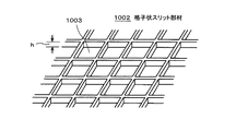
すなわち、特許文献4の指示体検出装置においては、図59の例と同様の複数個の上部電極Exが形成された電極シート1001と、第1の抵抗体層1002と、第2の抵抗体層1003と、図59の例と同様の複数個の下部電極Eyが形成された電極シート1004とが、x軸およびy軸に直交するz軸方向に積層されて配列される。
That is, in the pointer detection apparatus of
この場合に、図60(B)の図60(A)の断面図に示すように、電極シート1001に形成された上部電極Ex上に第1の抵抗体層1002が形成されて、上部電極Exと第1の抵抗体1002とが電気的に接続される。また、電極シート1004に形成された下部電極Ey上に第2の抵抗体1003が形成されて、下部電極Eyと第2の抵抗体1003とが電気的に接続される。そして、第1の抵抗体層1002と、第2の抵抗体層1003との間には、僅かな空隙AGが形成されるようにする。
In this case, as shown in the cross-sectional view of FIG. 60A of FIG. 60B, the
この例の指示体検出装置は、指などの指示体により、指示入力面、図の例では電極シート1001がZ軸方向に押圧されると、電極シート1001は、図60(C)の断面図に示すように、当該押圧部分が弾性的に変位して、第1の抵抗体層1002と第2の抵抗体層1003とが接触するようになる。そして、指示体からの指示入力面への押圧力が大きくなるほど、第1の抵抗体層1002と第2の抵抗体層1003との接触面積がおおきくなる。
In the pointer detection apparatus of this example, when the pointer, such as a finger, is pressed in the Z-axis direction, the
すると、当該押圧部分の上部電極Rxと下部電極Eyとの間には、第1の抵抗体層1002と第2の抵抗体層1003との両者の接触面積に応じた可変抵抗が介在するものとなる。この場合、この可変抵抗は、第1の抵抗体層1002と第2の抵抗体層1003との接触面積が大きくなればなるほど小さくなる。なお、図60(B)のように、指示体により押圧されていないときには、第1の抵抗体層1002と第2の抵抗体層1003とはほぼ非接触状態であるので、可変抵抗はほぼ無限大となる。
Then, a variable resistance corresponding to the contact area between the
したがって、図60(B)の状態で、上部電極Exと下部電極Eyとの一方の電極から電圧を印加しても、他方の電極にはその信号電流は伝達されない。そして、第1の抵抗体層1002と第2の抵抗体層1003とが接触すると、一方の電極からの信号電流が可変抵抗を介して他方の電極に流れ始める。そして、押圧力が大きくなるに従い、第1の抵抗体層1002と第2の抵抗体層1003との接触面積が大きくなると、一方の電極から他方の電極に流れる信号電流が、その接触面積に応じて大きくなる。
Therefore, even when a voltage is applied from one of the upper electrode Ex and the lower electrode Ey in the state of FIG. 60B, the signal current is not transmitted to the other electrode. When the
以上のことから、抵抗膜方式の指示体検出装置では、上部電極Exと下部電極Eyとの間の抵抗値の変化を検出することで、指示体により指示された位置が特定されると共に、その抵抗値により押圧力が検知される。 From the above, in the resistance film type indicator detection device, the change in the resistance value between the upper electrode Ex and the lower electrode Ey is detected, so that the position indicated by the indicator is specified. The pressing force is detected by the resistance value.
上述の静電結合方式の指示体検出装置においては、指示体が指示入力面に近づくあるいは接触した位置あるいは指示入力面からの指示体の離隔位置を検出することは可能であるが、入力面に対する押圧については検出することができないという問題がある。 In the electrostatic coupling type indicator detection apparatus described above, it is possible to detect the position at which the indicator approaches or contacts the instruction input surface, or the separation position of the indicator from the instruction input surface. There is a problem that pressing cannot be detected.
一方、抵抗膜方式を用いた指示体検出装置の場合には、指示体の指示入力面への接触(タッチ)位置の検知感度(初期指圧感度)が低く、また、指示入力面からの指示体の離隔位置の検出することは全くできないという問題がある。 On the other hand, in the case of the indicator detection device using the resistance film method, the detection sensitivity (initial sensitivity) of the contact (touch) position of the indicator on the instruction input surface is low, and the indicator from the instruction input surface is low. There is a problem in that it is impossible to detect the distance between the two.
この発明は、以上の点にかんがみ、指示体が指示入力面から離隔、あるいは接触した位置を検出することができると共に、指示体が指示入力面を押圧する状態における押圧力に応じた検出出力を得ることができる指示体検出装置を提供することを目的とする。 In view of the above points, the present invention can detect the position at which the indicator is separated from or in contact with the instruction input surface, and provides a detection output corresponding to the pressing force when the indicator presses the instruction input surface. An object of the present invention is to provide a pointer detection apparatus that can be obtained.
そして、この発明は、さらに、比較的簡単な構成で上記の指示体検出装置を実現することができるようにすることも目的とする。 Another object of the present invention is to realize the above indicator detection apparatus with a relatively simple configuration.
上記の課題を解決するために、この発明は、
第1の方向に配置された第1の複数の導体と、前記第1の方向に対して交叉する第2の方向に配置された第2の複数の導体と、前記第1の複数の導体と前記第2の複数の導体との間に配置された所定の抵抗特性を有する感圧材とを有する検出センサと、
前記第1の複数の導体に所定の信号を供給するための信号供給回路と、
前記第2の複数の導体から信号検出を行うための信号検出回路と、
を備え、
前記検出センサは、指示体が前記検出センサに接触した際に印加される圧力が所定の圧力よりも小さい場合には前記第1の複数の導体と前記第2の複数の導体との間の静電容量の変化に応じた信号を前記信号検出回路に供給し、前記指示体が前記検出センサに対して前記所定の圧力を超えた圧力を印加した場合には前記指示体からの前記圧力の前記感圧材への印加による前記第1の複数の導体と前記第2の複数の導体との間の抵抗特性の変化に応じた信号を前記信号検出回路に供給することで、
前記指示体による指示位置及び圧力を検知可能とした指示体検出装置を提供する。
In order to solve the above problems, the present invention provides:
A first plurality of conductors arranged in a first direction; a second plurality of conductors arranged in a second direction intersecting the first direction; and the first plurality of conductors; A detection sensor having a pressure sensitive material having a predetermined resistance characteristic disposed between the second plurality of conductors;
A signal supply circuit for supplying a predetermined signal to the first plurality of conductors;
A signal detection circuit for performing signal detection from the second plurality of conductors;
With
The detection sensor, when the pressure finger示体is applied upon contact with the detection sensor is smaller than a predetermined pressure between said first plurality of conductors and the second plurality of conductors A signal corresponding to a change in capacitance is supplied to the signal detection circuit, and when the indicator applies a pressure exceeding the predetermined pressure to the detection sensor, the pressure of the indicator from the indicator is changed. By supplying a signal corresponding to a change in resistance characteristics between the first plurality of conductors and the second plurality of conductors by application to the pressure-sensitive material to the signal detection circuit,
Provided is an indicator detection apparatus capable of detecting an indication position and pressure by the indicator.
上記の構成のこの発明の指示体検出装置によれば、信号検出回路は、第1の複数の導体と第2の複数の導体との間の静電容量の変化に応じた信号を検出し、その検出出力から指示体による検出センサへの例えば接触およびその位置を検出することができる。 According to the pointer detection apparatus of the present invention having the above-described configuration, the signal detection circuit detects a signal corresponding to a change in capacitance between the first plurality of conductors and the second plurality of conductors, For example, the contact and the position of the indicator to the detection sensor can be detected from the detection output.
また、信号検出回路は、第1の複数の導体と第2の複数の導体との間の抵抗特性の変化に応じた信号を検出し、その検出出力から指示体により検出センサへ圧力がかかっている指示位置を検出することができると共に、その圧力を検出することができる。 The signal detection circuit detects a signal corresponding to a change in resistance characteristics between the first plurality of conductors and the second plurality of conductors, and pressure is applied to the detection sensor by the indicator from the detection output. The indicated position can be detected, and the pressure can be detected.
すなわち、この発明の指示体検出装置によれば、信号検出回路で、第1の複数の導体と第2の複数の導体との間の静電容量の変化に応じた信号と、第1の複数の導体と第2の複数の導体との間の抵抗特性の変化に応じた信号を検出するという比較的簡単な構成で、指示体による指示位置及び圧力を検知可能である。 That is, according to the pointer detection apparatus of the present invention, in the signal detection circuit, the signal corresponding to the change in capacitance between the first plurality of conductors and the second plurality of conductors, and the first plurality The indication position and pressure by the indicator can be detected with a relatively simple configuration of detecting a signal corresponding to a change in resistance characteristics between the first conductor and the second plurality of conductors.
この発明によれば、比較的簡単な構成で、指示体の指示入力面への接触位置の検知感度が高く、指示体が指示入力面を押圧する状態における押圧力に応じた検出出力を得ることができる指示体検出装置を得ることができる。 According to the present invention, with a relatively simple configuration, the detection sensitivity of the contact position of the indicator on the instruction input surface is high, and a detection output corresponding to the pressing force when the indicator presses the instruction input surface is obtained. It is possible to obtain a pointer detection apparatus that can
以下、この発明による指示体検出装置の実施の形態を、図を参照しながら、以下の順序で説明する。 Embodiments of a pointer detection apparatus according to the present invention will be described below in the following order with reference to the drawings.
1.第1の実施の形態:基本構成例
2.第2の実施の形態:検出モードの切り替えを行わない例
3.第3の実施の形態:2つの検出モードを並行して実行する例
4.第4の実施の形態:拡散符号としてアダマール符号を用いる場合の改良構成例
5.第5の実施の形態:検出むらを除去する例
6.第6の実施の形態:増幅回路の自動利得制御
7.第7の実施の形態:大型のセンサ部の場合の例
8.第8の実施の形態:変調された拡散符号を用いる構成例
9.第9の実施の形態:拡散符号の他の供給方法
10.第10の実施の形態:受信導体の選択方法
11.第11の実施の形態:センサ部の他の構成例
[第1の実施の形態:基本構成例]
この実施の形態の指示体検出装置は、指示体の指示入力面との接触および指示体による指示入力面の押圧を検出するだけでなく、指示入力面上の空間における指示体の位置、指示体の指示入力面での接触位置および押圧位置(指示体座標位置)をも検出する。この例において、指示入力面上の空間における指示体の位置とは、指示入力面に接触せずに離隔した空間位置にある指示体の位置のことであり、この例では、指示体から指示入力面に対して垂線を下ろしたときの指示入力面の座標位置と、指示体の指示入力面からの離隔距離とから特定される。
1. 1. First embodiment: basic configuration example Second Embodiment: Example in which detection mode switching is not performed. 3. Third embodiment: Example of executing two detection modes in parallel 4. Fourth embodiment: Improved configuration example when Hadamard code is used as spreading
The indicator detection device of this embodiment not only detects the contact of the indicator with the instruction input surface and the pressing of the instruction input surface by the indicator, but also the position of the indicator in the space on the instruction input surface, the indicator The contact position and the pressed position (indicator coordinate position) on the instruction input surface are also detected. In this example, the position of the indicator in the space on the instruction input surface is the position of the indicator at a spatial position apart from the instruction input surface, and in this example, the instruction input from the indicator It is specified from the coordinate position of the instruction input surface when the perpendicular is drawn with respect to the surface and the separation distance of the indicator from the instruction input surface.
なお、この明細書において、指示入力面とは離隔した空間位置に指示体が存在する状態をホバーリング状態と称することとする。そして、この明細書において、指示体から指示入力面に対して垂線を下ろした方向をZ軸方向とし、指示入力面における座標位置は、互いに直交するX軸方向およびY軸方向の位置により定めるものとする。 In this specification, a state in which the indicator is present in a spatial position separated from the instruction input surface is referred to as a hovering state. In this specification, the direction in which the perpendicular from the indicator to the instruction input surface is defined as the Z-axis direction, and the coordinate position on the instruction input surface is determined by the X-axis direction and the Y-axis direction orthogonal to each other. And
また、指示体としては、以下の説明では、ユーザの指を主として用いる場合を説明するが、前述した静電ペン等を指示体として用いることもできる。 Further, in the following description, the case where the user's finger is mainly used will be described as the indicator, but the above-described electrostatic pen or the like can also be used as the indicator.
また、以下に説明する実施の形態は、指示入力面に同時に存在する複数の指示体、例えば複数本の指をも検出することが可能な例である。 The embodiment described below is an example in which a plurality of indicators, for example, a plurality of fingers, that exist simultaneously on the instruction input surface can be detected.
さらに、以下に説明する実施の形態は、指示入力面上における指示体の位置検出を、高速に行えるように工夫された構成を備える。 Furthermore, the embodiment described below has a configuration devised so that the position of the pointer on the instruction input surface can be detected at high speed.
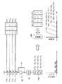
<第1の実施の形態の指示体検出装置の全体構成例:図1>
図1は、この第1の実施の形態の指示体検出装置1の全体の構成例を示すブロック図である。この実施の形態の指示体検出装置1は、検出センサの例であるセンサ部100と、送信部200と、受信部300と、送信部200及び受信部300の動作を制御する制御回路40とから構成される。以下、各部の構成について説明する。
<Example of Overall Configuration of Indicator Detection Device of First Embodiment: FIG. 1>
FIG. 1 is a block diagram showing an example of the overall configuration of the
制御回路40は、この実施の形態の指示体検出装置1の各部を制御するための回路であり、例えばマイクロコンピュータを搭載して構成されている。この制御回路40は、図1に示すように、送信部200の後述する送信信号供給回路21と、送信導体選択回路22と、クロック発生回路23とに接続されていると共に、受信部300の後述する受信導体選択回路31、増幅回路32、位置検出回路34とに接続されている。
The
そして、制御回路40は、後述するように、クロック発生回路23から出力されるクロック信号CLKに基づき、スタート信号ST、送信ロード信号Stload及び受信ロード信号Srloadを適宜生成及び出力して、上記各部の動作タイミングを制御する。
Then, as will be described later, the
<センサ部100の説明>
〔センサ部100の構成例:図1−図2〕
センサ部100について、図1および図2を参照して説明する。なお、図2(A)は、図1のセンサ部100におけるX軸方向断面図であり、図2(B)は、図1のセンサ部100におけるY軸方向断面図である。
<Description of
[Configuration Example of Sensor Unit 100: FIGS. 1-2]
The
センサ部100は、送信部200に接続される複数個の第1の電極と、受信部300に接続される複数個の第2の電極とを備えると共に、後述する感圧材を備える。以下の説明では、第1の電極は、送信導体と称し、複数の第1の電極からなる一群は、送信導体群11と称する。この実施の形態では、送信導体群11は、例えば64個の送信導体11Y1〜11Y64からなる。また、この実施の形態では、第2の電極は、受信導体と称し、複数の第2の電極からなる一群は、受信導体群12と称する。受信導体群12は、例えば128個の受信導体12X1〜12X128からなる。
The
なお、この明細書中で送信導体の説明において、送信導体群11中の64本の送信導体11Y1〜11Y64のいずれであるかを区別する必要のないときには、送信導体11Yと称することにする。同様に、受信導体の説明において、受信導体群12中の128本の受信導体12X1〜12X128のいずれであるかを区別する必要のないときには、受信導体12Xと称することにする。
In the description of the transmission conductor in this specification, when it is not necessary to distinguish between the 64
送信導体11Yは、指示入力面100Sの横方向(X軸方向)に延伸する直線状(板状)の導体である。この例では、送信導体11Yが、図2に示す下側基板16上に、図1に示すように、センサ部100の縦方向(Y軸方向)において、等間隔ずつ隔てて64本配列されることにより、送信導体群11が形成される。
The
また、受信導体12Xは、指示入力面100Sの縦方向(Y軸方向)に延伸する直線状(板状)の導体である。この例では、受信導体12Xが、図2に示す上側基板17の下側に、図1に示すように、センサ部100の横方向(X軸方向)において、等間隔ずつ隔てて128本配列されることにより、受信導体群12が形成される。
The receiving
上側基板17の上側面が、指や静電ペンなどの指示体により指示操作入力が行われる指示入力面100Sとされている。
The upper side surface of the
下側基板16と上側基板17とは、Z軸方向に所定の距離だけ隔てられている。そして、送信導体11Yと受信導体12XもZ軸方向に所定の距離だけ間隔を空けて互いに対向すると共に、送信導体11Yと受信導体12Xとは、延伸方向が互いに直交するように配置される。
The
上述のように構成されるので、複数本の送信導体11Yのそれぞれと、複数本の受信導体12Xのそれぞれとは、この例では、Z軸方向に所定の距離だけ間隔を空けた状態で、互いに直交する方向に交叉する。この明細書では、送信導体11Yと受信導体12Xとの交叉点をクロスポイントと称する。指示入力面100Sにおけるクロスポイントの座標位置は、指示体による指示入力の検出座標位置となる。
Since it is configured as described above, each of the plurality of
なお、直線状に形成された送信導体11Yと受信導体12Xとを直交するように配置した場合を例示して説明したが、送信導体11Yおよび受信導体12Xの形状は、実施の態様に応じて適宜設定される。また、送信導体11Yと受信導体12Xとは直交以外の角度、例えば、送信導体11Yと受信導体12Xとが斜めに交差する構成としても良い。また、送信導体11Y及び受信導体12Xの少なくとも一方を曲線状あるいは同心円状に形成した導体で構成してもよい。例えば複数の送信導体11Yをそれぞれ径の異なる円形状に形成し、これを同心円状に配置すると共に、複数の受信導体12Xを前記同心円の中心から放射状に延伸した直線形状の複数の導体により形成し、その複数の直線形状の導体を周方向に等角間隔で配置するようにしても良い。
In addition, although the case where the
また、電気特性上、受信導体12Xの幅は送信導体11Yの幅より細く形成すると良い。浮遊容量が減ることにより、受信導体12Xに混入するノイズを低減できるからである。
Further, in terms of electrical characteristics, the width of the
そして、送信導体11Yおよび受信導体12Xのそれぞれの配列間隔(ピッチ)は、例えば、ともに3.2mmとなるように形成される。なお、送信導体11Yおよび受信導体12Xの本数およびピッチはこれに限定されず、センサ部100のサイズや必要とする検出精細度等に応じて適宜設定される。
And the arrangement | positioning space | interval (pitch) of each of the
下側基板16および上側基板17は、例えば透明の合成樹脂等からなるシート状(フィルム状)の基板を用いる。上側基板17は、指示体により押圧されたときに押圧方向に弾性変位可能な材料で構成される。下側基板16は、弾性変位をする必要がないことから、ガラス基板や銅箔パターン基板で構成されていても良い。
For the
送信導体11Yおよび受信導体12Xは、例えば、銀パターンやITO(Indium Tin Oxide:酸化インジウムスズ)膜からなる透明電極膜、あるいは銅箔等で形成される。送信導体群11および受信導体群12の電極パターンは、例えば、次のように形成することができる。まず、上述した材料等で形成された電極膜を、例えば、スパッタ法、蒸着法、塗布法等により基板16および基板17上にそれぞれ形成する。次いで、形成した電極膜をエッチングして、所定の電極パターンの送信導体群11および受信導体群12をそれぞれ形成する。なお、送信導体11Yおよび受信導体12Xを銅箔で形成する場合には、銅箔エッジングの他、例えばインクジェットプリンタを用いて、銅粒子を含むインクをガラス板等上に吹き付けて所定の電極パターンを形成することもできる。
The
そして、感圧材は、第1の抵抗体と第2の抵抗体とからなる構成とされている。すなわち、図2に示すように、下側基板16上の送信導体11Y上には、第1の抵抗体(以下、送信抵抗体という)13Yが積層して形成される。また、上側基板17の下側の受信導体12X上には、第2の抵抗体(以下、受信抵抗体という)14Xが積層して形成される。送信抵抗体13Yと受信抵抗体14Xとは、指示入力面100Sに直交する方向において、僅かの空隙15の分だけ離隔されて設けられる。
The pressure sensitive material is configured by a first resistor and a second resistor. That is, as shown in FIG. 2, a first resistor (hereinafter referred to as a transmission resistor) 13 </ b> Y is laminated on the transmission conductor 11 </ b> Y on the
この例では、送信抵抗体13Yと受信抵抗体14Xとにおいて、空隙15を介して対向している面のそれぞれには、図2に示すように、極微な凹凸が形成されている。後述するように、送信抵抗体13Yと受信抵抗体14Xとが接触した状態における送信導体11Yと受信導体12X間の抵抗値は、送信抵抗体13Yおよび受信抵抗体14Xのこの凹凸が形成されている両対向面の接触面積に応じた値となる。
In this example, in the
なお、図示は省略するが、センサ部100の周縁部の下側基板16と上側基板17との間には、空隙15を維持するようにするためのスペーサ部材が設けられている。つまり、下側基板16と上側基板17とは、このスペーサ部材を介して接合されている。
Although not shown, a spacer member is provided between the
送信抵抗体13Yおよび受信抵抗体14Xは、指示体による押圧位置(X−Y座標位置)の検出感度および押圧力の検出感度を上げるために、送信導体11Yおよび受信導体12Xのそれぞれに対応して、分離した複数個からなる送信抵抗体および受信抵抗体として形成される。
The
すなわち、送信抵抗体13Yは、図2(B)に示すように、送信導体11Yのそれぞれを覆うと共に、隣接する送信抵抗体13Y同士が、空隙15Yにより離隔されて電気的に独立の状態となるように形成される。送信導体11Yを覆うように送信抵抗体13Yが設けられることにより、送信導体11Yと送信抵抗体13Yのそれぞれは、電気的に接続されている。
That is, as shown in FIG. 2B, the
同様に、受信抵抗体14Xは、図2(A)に示すように、受信導体12Xのそれぞれを覆うと共に、隣接する受信抵抗体14Y同士は、空隙15Xにより離隔されて電気的に独立の状態となるように形成される。受信導体12Xを覆うように受信抵抗体14Xが設けられることにより、受信導体12Xと送信抵抗体14Xのそれぞれは、電気的に接続されている。
Similarly, as shown in FIG. 2A, the
なお、送信抵抗体13Yおよび受信抵抗体14Xは、図60に示したように、基板16および基板17の一面の全体に設けるようにしても良い。ただし、送信抵抗体13Yおよび受信抵抗体14Xの双方を基板16および基板17の一面の全体に設けると、指示体の検出時に分解能が落ちるので、送信抵抗体13Yと受信抵抗体14Xのいずれか一方は、上述の例のように分離された複数の抵抗体の構成とした方が良い。
The
送信抵抗体13Yおよび受信抵抗体14Xは、例えばITO(Indium Tin Oxide:酸化インジウムスズ)やATO(アンチモンドープ酸化スズ)などの透明な抵抗膜で構成される。なお、指示体検出装置1が表示画面の前面に配する必要のない用途に用いられる場合には、送信抵抗体13Yおよび受信抵抗体14Xを構成する材料は、透明の抵抗膜材料に限られるものではないことは言うまでもない。
The
この発明の指示体検出装置は、液晶パネル等の表示装置とを一体構成することができるものであるが、その場合は、センサ部100は、液晶パネル上に重ねられて設けられるものである。
The pointer detection apparatus of the present invention can be configured integrally with a display device such as a liquid crystal panel. In this case, the
〔センサ部100における指示体検出の原理説明:図3−図10〕
この実施の形態では、送信部200からセンサ部100の送信導体11Yのそれぞれに対して後述する送信信号が供給される。この送信信号は、電圧信号として送信導体11Yに供給される。この送信信号(電圧信号)は送信導体11Yと受信導体12Xとの間の静電容量Coに供給される。当該静電容量Coには、指示体の有無に応じて変化する電流が流れ、この電流が受信導体12Xに流れる。
[Description of Principle of Indicator Detection in Sensor Unit 100: FIGS. 3 to 10]
In this embodiment, a transmission signal described later is supplied from the
また、後述するように、指示体により指示入力面100Sに押圧力が印加されて、送信抵抗体13Yと受信抵抗体14Xとが接触する状態のときには、前記押圧力に応じて送信抵抗体13Yと受信抵抗体14Xとの接触面積が変わる。そして、送信導体11Yに供給された送信信号(電圧信号)により、送信抵抗体13Yと受信抵抗体14Xとの接触面積に応じた電流が受信導体12Xに流れる。
As will be described later, when the pressing force is applied to the pointing
受信導体12Xに流れる電流は、受信信号として受信部300に供給される。受信部300は、信号検出回路を構成するもので、電流信号として受信した受信信号を電圧信号に変換し、後述するようにして指示体検出結果を得るようにする。なお、以下に説明する原理説明では、簡単のため、同一の送信信号が、64本の送信導体11Y1〜11Y64に、順次に送信タイミングをずらして供給される場合を想定する。
The current flowing through the
<指示体が指示入力面から離隔した状態から接触までの検出;静電結合方式、図3−図5>
この場合に、センサ部100の上側基板17の表面である指示入力面100S上に指などの指示体が存在しないときには、送信導体11Yに供給された送信信号(電圧信号)により、受信導体12Xと送信導体11Yとのクロスポイントにおける静電容量Coに電流が流れる。その電流は受信導体12Xに流れて、受信部300に受信信号(電流信号)として供給される。これは、指示入力面100Sの全てのクロスポイントにおいて同様となるので、指示入力面100S上に指などの指示体が存在しないときには、受信導体12X1〜12X128の全てから、図4(A)に示すように、同レベル(同じ電流値)の受信信号が受信部300に供給される。
<Detection from the state where the indicator is separated from the instruction input surface to contact; electrostatic coupling method, FIG. 3 to FIG. 5>
In this case, when there is no indicator such as a finger on the
なお、図4(A)は、任意の1本の送信導体11Yと交叉する128本の受信導体12X1〜12X128についての128個のクロスポイントに流れる電流、すなわち、各受信導体12X1〜12X128から得られる受信信号を示すものである。指示入力面100S上に指などの指示体が存在しないときには、その他の全ての送信導体11Yと128本の受信導体12X1〜12X128とのクロスポイントにおいても同様に、図4(A)に示すように、受信導体12Xから受信部300に供給される受信信号は、同レベルとなる。
Incidentally, FIG. 4 (A), the current flowing through the 128 cross points of the
一方、図3に示すように、指示入力面100S上において、指示体18の例としての指が、指示入力面100Sとは離隔した近接位置に置かれたり、指示入力面100Sと接触する位置に置かれて指示入力されると、その指示入力位置においては、指示体18と受信導体12Xとの間での結合により静電容量Cfa、Cfbが生じる。すると、指示体18による指示入力位置に対応するクロスポイントにおいては、送信信号(電圧信号)により静電容量Coに流れる電流の一部が、静電容量Cfa、Cfbを通じて消失するようになる。
On the other hand, as shown in FIG. 3, on the
すなわち、センサ部100の指示入力面100S上に指示体18が存在する場合には、図3に示すように、当該指示体18による指示入力位置の送信導体11Yは、受信導体12Xだけでなく、指示体18を介してグラウンドと静電結合した状態となる。この状態では、図3において矢印で示すように、送信信号に応じて送信導体11Yに接続される送信抵抗体13Yから出た電気力線は、受信抵抗体14Xを通じて受信導体12Xに収束するのみではなく、その一部が指示体18にも収束する。そのため、送信信号に応じて受信導体12Xに流れる電流の一部が指示体18を介してグラウンドに分流する。その結果、図4(B)に示すように、指示体18による指示入力位置の受信導体12Xに流れる電流は、指示体18が存在しないときの値ref(これを基準値とする)よりも減少する。
That is, when the
この基準値refよりも減少する電流変化を検出することで、指示入力面100Sに対して離隔した位置から接触位置までの指示体18による指示入力面100S上での指示入力位置を検出する。そして、その減少する電流変化が生じたクロスポイントの位置を検出することにより、指示入力面100Sに対して離隔した位置から接触位置までの指示体18による指示入力位置を検出する。指示体18による指示入力位置の検出については、後で詳述する。
By detecting a current change that is smaller than the reference value ref, the instruction input position on the
以上のように、指示体18が指示入力面100Sとは離隔したホバーリング状態から指示入力面100Sと接触する状態までの間に存在する場合においては、この実施の形態では、静電結合方式により、指示体検出がなされる。
As described above, when the
この静電結合方式において受信導体12Xから得られる電流信号としての受信信号は、受信部300において、電圧信号に変換される。図5は、静電結合方式における電流−電圧変換回路(以下、I/V変換回路という)の基本構成例を示す図である。
In the electrostatic coupling method, a reception signal as a current signal obtained from the
すなわち、静電結合方式において受信導体12Xからの受信信号(電流信号)に対して設けられるI/V変換回路は、図5に示すように、演算増幅器51の入出力端間に検出用コンデンサ52が接続されて構成される。なお、実際的には、検出用コンデンサ52には並列に直流バイアス用の抵抗53が接続されるものである。
That is, the I / V conversion circuit provided for the reception signal (current signal) from the
<指示体による指示入力面への押圧力の検出;抵抗膜方式、図6−図8>
上述した、指示体が指示入力面から離隔した状態から接触までの指示体入力面に押圧力が印加されていない状態においては、送信抵抗体13と受信抵抗体14とは、空隙15を隔てて離隔した状態であり、これら送信抵抗体13と受信抵抗体14とを通じて電流が流れることはない。したがって、指示体入力面100Sに指示体18による押圧力が印加されていない状態では、図7(A)に示すように、送信抵抗体13と受信抵抗体14とを通じて電流は流れず、受信導体12Xに流れる電流は一定(=基準値ref)となる。
<Detection of pressure applied to the input surface by the indicator; resistive film system, FIGS. 6 to 8>
In the state where the pressing force is not applied to the indicator input surface from the state in which the indicator is separated from the instruction input surface to the contact described above, the
図6に示すように、指示体18により、指示入力面100Sに対して、接触している状態からさらに、押圧力が印加されると、その押圧力が印加された上側基板17の部位が変位させられ、その部位の受信抵抗体14Xと送信抵抗体13Yの両対向面が接触する状態になる。
As shown in FIG. 6, when a pressing force is further applied by the
すると、送信導体11Yに供給された送信信号(電圧信号)により、押圧力が印加された位置の受信導体12Xに、接触した受信抵抗体14Xと送信抵抗体13Yにより形成される可変抵抗VRの抵抗値を介して電流が流れることになる。すなわち、押圧力が印加された位置においては、送信導体11Yから受信導体12Xに対して、当該押圧力が印加された部位の受信抵抗体14Xと送信抵抗体13Yとの接触部分の可変抵抗VRの抵抗値に応じた電流が流れる(図7(B)参照)。
Then, the resistance of the variable resistor VR formed by the receiving
受信抵抗体14Xと送信抵抗体13Yとの接触部分の可変抵抗VRの抵抗値は、その接触面積が大きくなるほど小さくなり、可変抵抗VRを流れる電流は、接触面積が大きくなるほど大きくなる。前述したように、送信抵抗体13Yと受信抵抗体14Xとが接触する面は、極微な凹凸が形成されており、指示体18による指示入力面100Sに対する押圧力が大きくなればなるほど前記凹凸間の空隙がなくなって、受信抵抗体14Xと送信抵抗体13Yとの接触面積は、大きくなる。
The resistance value of the variable resistor VR at the contact portion between the
したがって、指示体18により、指示入力面100Sに対して押圧力が印加されると、その押圧力が印加された部位では、前記可変抵抗VRを通じて送信導体11Yから受信導体12Xに電流が流れ始め、その電流量は、押圧力に応じて大きくなる。つまり、押圧力が印加されていないときには送信抵抗体13と受信抵抗体14とは接触していないため、可変抵抗VRを通じた電流は流れず、受信導体12Xから得られる電流は基準値refとなっているが、押圧力が印加されて送信抵抗体13と受信抵抗体14とが接触する状態になると、前記可変抵抗VRを通じて電流が流れて、受信導体12Xから得られる電流は、基準値refよりも増加する方向に変化する。
Therefore, when a pressing force is applied by the
この基準値refよりも増加する方向の電流変化を検出することで、指示体18によって指示入力面100Sに印加された押圧力を検出する。そして、基準値refよりも増加する方向の電流変化が生じたクロスポイントの位置を検出することにより、指示入力面100Sに対して指示体18により押圧力が印加された指示入力位置を検出する。
By detecting a current change in a direction increasing from the reference value ref, the pressing force applied to the
以上のように、指示体18による指示入力面100Sへの押圧力を伴う指示入力については、抵抗膜方式により、指示体の検出がなされる。
As described above, for the instruction input accompanied by the pressing force to the
この抵抗膜方式において受信導体12Xから得られる電流も、静電結合方式の場合と同様に、受信部300において、電圧に変換される。ただし、抵抗膜方式の場合には、電流検出用の素子が、コンデンサではなく抵抗とされる点が静電結合方式の場合と異なる。
The current obtained from the receiving
図8は、抵抗膜方式におけるI/V変換回路の基本構成例を示す図である。抵抗膜方式において受信導体12Xから受信部300に供給される受信信号(電流信号)に対して設けられるI/V変換回路は、図8に示すように、演算増幅器51の入出力端間に検出用抵抗54が接続されて構成される。
FIG. 8 is a diagram illustrating a basic configuration example of an I / V conversion circuit in the resistive film system. In the resistive film system, an I / V conversion circuit provided for a reception signal (current signal) supplied from the
以上説明したように、この実施の形態では、センサ部100では、静電結合方式の指示体検出(ホバーリング検出を含む)と、抵抗膜方式の指示体検出(押圧検出を含む)が可能である。
As described above, in this embodiment, the
制御回路40は、受信部300に供給される受信信号(電流信号)の変化に基づいて、受信部300で実行する指示体の検出処理を、静電結合方式あるいは抵抗膜方式のいずれの方式で実行するかを判断する。具体的には、制御回路40は、受信導体12Xから受信部300に供給される受信信号について、基準値refよりも減少する方向に電流変化が生じたときには、受信部300で静電結合方式で指示体検出をするように制御し、基準値refよりも増加する方向に電流変化が生じたときには、受信部300で抵抗膜方式で指示体の検出をするように制御する。なお、制御回路40ではなく、受信部300に、いずれの指示体検出方式で指示体の検出を実行するかの判定手段を設けて、受信部300での指示体検出方式をいずれにするかを制御するようにしても良い。
The
なお、この明細書の以下の説明において、静電結合方式での指示体検出モードを、キャパシティブタッチ検出モードと称し、抵抗膜方式での指示体検出モードを、レジスティブタッチ検出モードと称することとする。 In the following description of this specification, the indicator detection mode in the electrostatic coupling method is referred to as a capacitive touch detection mode, and the indicator detection mode in the resistance film method is referred to as a resistive touch detection mode. To do.
<この実施の形態で用いるI/V変換回路の構成例>
この実施の形態では、I/V変換回路は、上述した静電結合方式と抵抗膜方式の両方の指示体検出方式を可能にする構成とする必要がある。静電結合方式と抵抗膜方式の両方の指示体検出方式を可能にするI/V変換回路の構成例について、以下に説明する。
<Configuration example of I / V conversion circuit used in this embodiment>
In this embodiment, the I / V conversion circuit needs to be configured to enable both the electrostatic coupling method and the resistive film method of detecting the indicator. A configuration example of an I / V conversion circuit that enables both the electrostatic coupling method and the resistive film method of detecting an indicator will be described below.
〔第1の構成例:図9〕
図9に、この実施の形態で用いるI/V変換回路の第1の構成例を示す。このI/V変換回路の第1の構成例においては、静電結合方式と抵抗膜方式とをスイッチ回路55により切り替える。
[First configuration example: FIG. 9]
FIG. 9 shows a first configuration example of the I / V conversion circuit used in this embodiment. In the first configuration example of the I / V conversion circuit, the
すなわち、この第1の構成例においては、演算増幅器51の入出力端間には、外部からの切替制御信号SW1により端子Cと端子Rとに切り替え可能なスイッチ回路55と、静電結合方式における検出用コンデンサ52と、抵抗膜方式における検出用抵抗54とが設けられる。
That is, in the first configuration example, between the input and output terminals of the
そして、このスイッチ回路55の端子C側と、演算増幅器51の出力端との間には、静電結合方式における検出用コンデンサ52が接続される。なお、検出用コンデンサ52には、直流バイアス抵抗53が接続されている。また、このスイッチ回路55の端子R側と、演算増幅器51の出力端との間には、抵抗膜方式における検出用抵抗54が接続される。
A
この第1の構成例においては、指示体検出装置1は、キャパシティブタッチ検出モードと、レジスティブタッチ検出モードの2つの指示体検出モードを備えている。そして、切替制御信号SW1は、制御回路40または受信部300において、前述した静電結合方式あるいは抵抗膜方式のいずれの指示体検出方式で指示体検出処理を実行するかの判定手段の判定結果から生成されて、スイッチ回路55に供給される。すなわち、制御回路40または受信部300は、センサ部100から入力される電流信号に基づいて切替制御信号SW1を生成する。
In the first configuration example, the
そして、キャパシティブタッチ検出モードにおいては、スイッチ回路55は、この切替制御信号SW1により、端子C側に切り替えられ、演算増幅器51の入出力端間に検出用コンデンサ52を接続する。
In the capacitive touch detection mode, the
また、レジスティブタッチ検出モードにおいては、スイッチ回路55は、切替制御信号SW1により、端子R側に切り替えられ、演算増幅器51の入出力端間に検出用抵抗54を接続する。
Further, in the resistive touch detection mode, the
なお、図9の例では、スイッチ回路55は、演算増幅器51の入力端側に設けたが、演算増幅器51の出力端側に設けても勿論よい。
In the example of FIG. 9, the
〔第2の構成例:図10〕
この第2の構成例は、キャパシティブタッチ検出モードと、レジスティブタッチ検出モードの2つのモードに共用できるI/V変換回路の一例である。すなわち、キャパシティブタッチ検出モードと、レジスティブタッチ検出モードとに応じた切り替えを不要とした例である。
[Second Configuration Example: FIG. 10]
The second example, a capacitive touch detection mode, which is an example of the I / V conversion circuit can be shared in two modes of the resistive touch detection mode. That is, in this example, switching according to the capacitive touch detection mode and the resistive touch detection mode is unnecessary.
図10に、この実施の形態で用いるI/V変換回路の第2の構成例を示す。このI/V変換回路の第2の構成例においては、演算増幅器51の入出力端間に、静電結合方式の検出用コンデンサ52と、抵抗膜方式の検出用抵抗54とを並列に接続する構成とする。
FIG. 10 shows a second configuration example of the I / V conversion circuit used in this embodiment. In the second configuration example of the I / V conversion circuit, an electrostatic
この場合、図5に示したように、検出用コンデンサ52には、直流バイアス用抵抗53が接続されている。したがって、抵抗膜方式の検出用抵抗54が検出用コンデンサ52の直流バイアス用抵抗53と等しい抵抗値であれば、第1の構成例のようなモード切り替えスイッチ回路55は不要となる。すなわち、この場合、検出用抵抗54の抵抗値Rが、検出用コンデンサ52の静電容量をCとしたとき、
R≒1/jωC
を満足する場合に、I/V変換回路は、この第2の構成例とすることができる。
In this case, as shown in FIG. 5, a
R ≒ 1 / jωC
In the case of satisfying the above, the I / V conversion circuit can be the second configuration example.
この第2の構成例では、キャパシティブタッチ検出モードと、レジスティブタッチ検出モードとの切り替えは、基本的に不要になる。なお、いずれの検出モードで指示体検出を行ったかを検知して、そのモード検出結果を出力するようにする場合には、第1の構成例と同様に、制御回路40または受信部300で、いずれの検出方式で指示体検出を行うかを判定し、その判定結果を出力するようにする。
In the second configuration example, switching between the capacitive touch detection mode and the resistive touch detection mode is basically unnecessary. In addition, when detecting in which detection mode indicator detection has been performed and outputting the mode detection result, in the
<指示体の指示入力位置(クロスポイント位置)を検出するための構成部分の説明>
この実施の形態では、静電結合方式の指示体検出の場合と、抵抗膜方式の指示体検出の場合とで、指示体の指示入力位置の検出の仕方に関しては、全く同様の検出処理動作がなされる。
<Description of Component for Detecting Instruction Input Position (Cross Point Position) of Indicator>
In this embodiment, exactly the same detection processing operation is performed with respect to the method of detecting the pointing input position of the pointer in the case of electrostatic coupling type pointer detection and in the case of resistance film type pointer detection. Made.
送信導体11Yのそれぞれと受信導体12Xのそれぞれとの全てのクロスポイントにおいて、静電結合方式の指示体検出と抵抗膜方式の指示体検出を実行すれば、いずれのクロスポイントで指示体による指示入力がなされたかの位置検出が可能である。
If electrostatic coupling type indicator detection and resistive film type indicator detection are executed at all cross points between each of the
この場合には、1個(1種類)送信信号を全てのクロスポイントの送信導体に順次に供給するようにすると共に、受信部300において、送信信号が送信導体に供給されたクロスポイントの受信導体からの受信信号について指示体検出を行なうことにより、指示体による指示入力位置の検出が可能である。しかし、このようにしたのでは、多数のクロスポイントの一つ一つ毎に指示体検出を実行することになるため、指示入力面100Sの全てのクロスポイントについての指示体検出の結果を得られるまでに長時間がかかり、実用上好ましくない。
In this case, one (one type) transmission signal is sequentially supplied to all the cross-point transmission conductors, and in the
一方、送信信号を送信導体11Yの本数分だけ複数個用意すると共に、受信部300において受信導体12Xのそれぞれに対してI/V変換回路を設けて、指示体検出を行うように構成することも考えられる。この場合には、全ての送信導体11Yに、受信部300で弁別可能な異なる送信信号を同時に供給すると共に、受信部300において、全ての受信導体からの受信信号を、それぞれのI/V変換回路により同時に電圧信号に変換して、指示体検出をする。受信部300では、複数のI/V変換回路からの受信信号を同時に処理することで、指示入力面100Sの全てのクロスポイントについての指示体検出結果が得られるので、非常に高速に処理結果が得られる。
On the other hand, a plurality of transmission signals corresponding to the number of
しかし、そのようにした場合には、ハードウエア構成が膨大になり、コスト高となると共に、指示体検出装置が大型になってしまうという問題がある。 However, in such a case, there is a problem that the hardware configuration becomes enormous, the cost is increased, and the pointer detection apparatus becomes large.
この実施の形態では、この問題点にかんがみ、ハードウエア規模が膨大にならないことを考慮しながら、高速に指示体検出結果が得られるように、送信部200および受信部300を構成している。
In this embodiment, in consideration of this problem, the
すなわち、この実施の形態では、送信導体群11の複数本の送信導体11Yは、それぞれ同数の複数本の送信導体11Yからなる複数個のグループに分割し、それぞれのグループ毎に、異なる送信信号を割り当てる。以下の説明においては、複数本の送信導体11Yからなるグループを送信ブロックと称することとする。異なる送信信号としては、後述するように、この実施の形態では、符号が異なる拡散符号が用いられる。
That is, in this embodiment, the plurality of
この実施の形態では、複数個の送信ブロックのそれぞれに含まれる複数本の送信導体11Yから選択した1本の送信導体11Yに、前記異なる送信信号を同期させて同時に供給する。そして、各送信ブロックにおいて、選択する1本の送信導体を切り替えて、切り替え後の送信導体11Yのそれぞれに、送信ブロック毎に異なる送信信号を同期させて同時に供給する動作を繰り返す。送信ブロック内の全ての送信導体11Yへの送信信号の供給が終了したら、当該送信ブロック内で最初に選択した送信導体11Yを選択する状態に戻り、以上の処理を繰り返す。
In this embodiment, the different transmission signals are simultaneously supplied in synchronization to one
これにより、受信導体12Xのそれぞれには、複数個の送信ブロックからの異なる送信信号(電圧信号)に応じた電流が多重された状態で流れることになる。そして、後述するように、受信部300は、この受信導体12Xのそれぞれからの電流信号のそれぞれを、送信信号の送信タイミングに同期して検出することができるように構成される。
As a result, currents corresponding to different transmission signals (voltage signals) from a plurality of transmission blocks flow through the
すなわち、この実施の形態では、送信信号として符号が異なる拡散符号を用いるので、受信部300では、その異なる拡散符号のそれぞれについての相関値を、同時並列的に検出するようにする。そして、その検出した相関値に基づいて、受信導体12Xを流れる電流の変化を検出することにより、指示体により指示入力面100S上のいずれのクロスポイントにおいて指示入力されたかどうかの検出出力を得るようにする。
That is, in this embodiment, since spread codes having different codes are used as transmission signals, the receiving
制御回路40は、上述のような送信部200および受信部300での動作を実現するために、各送信ブロック内の複数本の送信導体11Yについての前述した切り替えタイミングに同期して、受信部300における受信導体12Xについての切り替えタイミングを制御する。
In order to realize the operations of the
以上のように構成することにより、送信ブロックの数をN(Nは2以上の整数)とすると、全てのクロスポイントを順次にサーチする場合のN倍の速度(処理時間が1/N)で、指示体検出処理が可能となる。 By configuring as described above, assuming that the number of transmission blocks is N (N is an integer of 2 or more), the speed is N times that when all cross points are searched sequentially (processing time is 1 / N). The indicator detection process can be performed.
〔送信部200の構成例:図11−図13〕
上述の機能を満足するために、この実施の形態の送信部200は、送信信号供給回路21と、送信導体選択回路22と、クロック発生回路23とを備えて構成される。
[Configuration Example of Transmitter 200: FIGS. 11 to 13]
In order to satisfy the above-described functions, the
この実施の形態では、図11に示すように、64本の送信導体11Y1〜11Y64は、例えば4本ずつからなる16個の送信ブロックTB1〜TB16に分割される。したがって、送信信号供給回路21は、16個の異なる送信信号を発生する必要があるが、この例では、送信信号として、16個の異なる拡散符号が用いられる。
In this embodiment, as shown in FIG. 11, the 64
なお、異なる拡散符号としては、一つの拡散符号を1チップ分あるいは複数チップ分ずつ位相をずらしたものを用いることもできる。 In addition, as a different spreading code, one spreading code whose phase is shifted by one chip or a plurality of chips can be used.
特にこの例においては、送信ブロック数に合わせて、図12に示すような16行×16列のアダマール行列を考え、このアダマール行列を構成する各行(各列でも同じ)の16チップのアダマール符号を、16個の拡散符号C1〜C16として用いる。この16個のアダマール符号は、互いに直交関係を有する符号列である。 Particularly in this example, a 16-row × 16-column Hadamard matrix as shown in FIG. 12 is considered according to the number of transmission blocks, and a 16-chip Hadamard code of each row (same in each column) constituting the Hadamard matrix is used. , 16 spread codes C 1 to C 16 are used. The 16 Hadamard codes are code strings that are orthogonal to each other.
この例の送信信号供給回路21は、図11に示すように、16個の拡散符号生成回路2101,2102,・・・,2116からなる。拡散符号生成回路2101,2102,・・・,2116は、互いに直交するアダマール符号からなる拡散符号C1,C2,・・・,C16をそれぞれ発生する
拡散符号生成回路2101,2102,・・・,2116には、それぞれクロック発生回路23からクロック信号CLKが入力される。なお、クロック発生回路23から出力されたクロック信号CLKは、タイミング信号として制御回路40にも入力される。
As shown in FIG. 11, the transmission
各拡散符号生成回路2101,2102,・・・,2116は、制御回路40の制御に基づき、クロック発生回路23から供給されたクロック信号CLKに同期して1チップ毎に、拡散符号C1,C2,・・・,C16を出力する。この例では、各拡散符号生成回路2101,2102,・・・,2116は、それぞれクロック信号CLKの1周期毎に、拡散符号の1チップのデータを生成することで、クロック信号CLKの16周期分で、それぞれ16チップPN1,PN2,・・・,PN16からなる拡散符号C1,C2,・・・,C16を生成する。すなわち、この拡散符号生成回路2101,2102,・・・,2116は、クロック信号CLKの16周期分毎に、16チップPN1,PN2,・・・,PN16からなる拡散符号C1,C2,・・・,C16をそれぞれ、周期的に繰り返し、生成する。
Each of the spread
なお、以下の説明においては、便宜上、クロック信号CLKの16周期分である16チップPN1,PN2,・・・,PN16分を、拡散符号C1,C2,・・・,C16の1周期分と称することとする。
In the following description, for convenience, the
拡散符号生成回路2101,2102,・・・,2116は、生成した拡散符号C1,C2,・・・,C16を送信導体選択回路22に供給する。
, 2116 supplies the generated spread codes C 1 , C 2 ,..., C 16 to the transmission
なお、この送信信号供給回路21は、ROMなどからなる不揮発性メモリに、拡散符号C1,C2,・・・,C16のデータを予め保持しておき、その不揮発性メモリの読み出しアドレスを制御することで、複数個の拡散符号C1,C2,・・・,C16を出力する構成にしてもよい。
The transmission
送信導体選択回路22は、図11に示すように、16個の送信ブロックTB 1 〜TB 16 のそれぞれに対応する16個のスイッチ回路2201〜2216からなる。スイッチ回路2201〜2216のそれぞれは、1入力4出力のスイッチ回路である。これらのスイッチ回路2201〜2216のそれぞれには、対応する拡散符号生成回路2101〜2116のそれぞれからの拡散符号C1,C2,・・・,C16が入力される。そして、スイッチ回路2201〜2216のそれぞれは、対応する送信ブロックTB 1 〜TB 16 のそれぞれを構成する4本の送信導体11Yのうちの1本の送信導体を選択的に前段の拡散符号生成回路2101〜2116に接続して、拡散符号を供給する。
As illustrated in FIG. 11, the transmission
スイッチ回路2201は、送信ブロックTB 1 に対応するものであり、当該スイッチ回路2201に入力される拡散符号C1を供給する送信導体として、送信ブロックTB 1 の4本の送信導体11Y1,11Y2,11Y3,11Y4を1本ずつ順次に切り替える。また、スイッチ回路2202は、送信ブロックTB 2 に対応するものであり、当該スイッチ回路2202に入力される拡散符号C2を供給する送信導体として、送信ブロックTB 2 の4本の送信導体11Y5,11Y6,11Y7,11Y8を1本ずつ順次に切り替える。その他のスイッチ回路2203〜2216のそれぞれについても同様であり、それぞれに入力される拡散符号を供給する送信導体として、対応する送信ブロックTB 3 〜TB 16 のそれぞれ内の4本の送信導体を1本ずつ順次に切り替える。
The switch circuit 2201 sends are those corresponding to the block TB 1, the switch circuit 2201 as a transmission conductors for supplying the spread codes C 1 to be input to the four
これらスイッチ回路2201〜2216には、制御回路40から切替制御信号SW2が供給される。制御回路40は、クロック信号CLKからこの切替制御信号SW2を生成する。制御回路40は、拡散符号の1周期分であるクロック信号CLKの16周期分を1周期とするパルス信号として切替制御信号SW2を生成する。
The switch circuits 2201 to 2216 are supplied with a switching control signal SW2 from the
スイッチ回路2201〜2216は、この切替制御信号SW2により、クロック信号CLKの16周期分毎に、拡散符号を供給する送信導体11Yを切り替えられる。すなわち、スイッチ回路2201〜2216は、切替制御信号SW2により、それぞれが選択中の送信導体11Yに16チップからなる拡散符号の1周期分を供給し終わった後、次の送信導体11Yに切り替える。
The switch circuits 2201 to 2216 can switch the
このときのスイッチ回路2201〜2216の切り替え動作例を図13に示す。この図13の例においては、スイッチ回路2201〜2216により、最初に、16本の送信導体11Y4,11Y8,・・・,11Y60,11Y64が選択される。そして、このスイッチ回路2201〜2216により選択された送信導体11Y4,11Y8,・・・,11Y60,11Y64に、拡散符号C1,C2,・・・,C15,C16のそれぞれが供給される。
An example of the switching operation of the switch circuits 2201 to 2216 at this time is shown in FIG. In the example of FIG. 13, 16
この状態で、クロック信号CLKの16周期分が経過すると、拡散符号C1,C2,・・・,C15,C16のそれぞれの1周期分が、16本の送信導体11Y4,11Y8,・・・,11Y60,11Y64に供給し終わる。そして、この時点において、切替制御信号SW2により、スイッチ回路2201〜2216のそれぞれは、選択する送信導体11Yを、この例ではインデックス番号が小さくなる隣りの送信導体に切り替えられる。
In this state, when 16 cycles of the clock signal CLK have elapsed, each of the spreading codes C 1 , C 2 ,..., C 15 , C 16 has 16
そして、各送信ブロックTB 1 〜TB 16 内の最小インデックス番号の送信導体Y1,Y5,…,Y57およびY61がスイッチ回路2201〜2216により選択され、拡散符号C1〜C16の供給が行われた後は、再度、各送信ブロック内の最大インデックス番号の送信導体11Y4,11Y8,・・・,11Y60,11Y64がスイッチ回路2201〜2216により選択される。上記切り替え動作が各送信ブロック内で繰り返されることで、すべての送信導体11Yに対し拡散符号C1〜C16が供給される。
Then, the transmission conductors Y 1 , Y 5 ,..., Y 57 and Y 61 having the smallest index number in each of the transmission blocks TB 1 to TB 16 are selected by the switch circuits 2201 to 2216, and supply of spreading codes C 1 to C 16 is performed. After that, the
以上のようにして、送信部200においては、複数個の送信ブロックにおいて、同期して、送信導体11Yの切り替えがなされることにより、送信ブロック毎に異なる複数個の拡散符号が、複数本の送信導体11Yに同時に供給される。したがって、送信信号をセンサ部100の全送信導体に供給する時間が、1本ずつの送信導体に送信信号を供給する場合の送信ブロック数分の1にすることができるので、センサ部100の全送信導体に供給する時間を短縮することができる。
As described above, in the
そして、全ての送信導体11Yに対して異なる送信信号を用意する場合に比べると、送信信号をセンサ部100の全送信導体に供給する時間は遅くなるが、送信信号とされる複数の拡散符号は、送信ブロック数の分の1にすることができるので、その分だけ回路規模を、比較的小規模にすることが可能である。
And compared with the case where different transmission signals are prepared for all the
なお、スイッチ回路2201〜2216の切替動作の手順は上述の例に限定されない。例えば、各送信ブロック内での送信導体11Yの切り替えは、拡散符号の1周期分毎に行うようにしたが、拡散符号の複数周期分毎に行っても良い。また、拡散符号は、1チップを、送信ブロック内の送信導体数分のクロック信号CLKの周期毎に発生するようにして生成し、各送信ブロック内での送信導体11Yの切り替えは、クロック信号CLKの1周期分毎に行うようにしてもよい。
Note that the procedure of the switching operation of the switch circuits 2201 to 2216 is not limited to the above example. For example, the switching of the
〔受信部300の構成例:図14−図22〕
受信部300は、受信導体12Xのそれぞれから得られる受信信号(電流)を増幅すると共に、前述した電流変化を検出する信号処理をすることにより、指示体の検出を行うようにする。
[Configuration Example of Receiving Unit 300: FIGS. 14 to 22]
The receiving
ここで、各受信導体12Xから得られた受信信号に対して上記の信号処理を順次に行うと、その完了までに長時間を要してしまう。そこで、各受信導体12Xに上記の信号処理を行う専用の処理回路を設けて、全ての受信信号について同時に信号処理を行うようにして高速化を実現することが考えられる。しかし、それでは回路規模やコストの問題があって現実的はない。
Here, if the above signal processing is sequentially performed on the reception signals obtained from the
そこで、この実施の形態では、受信部300においては、複数本の受信導体12Xで、処理回路を共用するように構成することにより、回路規模を小規模にするようにしている。すなわち、受信導体群12の複数本の受信導体12Xを、それぞれ同数の複数本の受信導体12Xからなる複数個のグループに分割し、それぞれのグループに対して、増幅器およびI/V変換回路等を設けるようにする。以下の説明においては、複数本の受信導体12Xからなるグループを検出ブロックと称することとする。
Therefore, in this embodiment, the receiving
この例では、受信導体群12を構成する複数の受信導体12X1〜12X128は、図14に示すように、8本ずつからなる16個の検出ブロックDB1〜DB16に分割される。そして、16個の検出ブロックDB1〜DB16のそれぞれに含まれる8本の受信導体12Xから、1本の受信導体12Xを順次に切り替え選択して受信部300の処理を実行する。このように構成することにより、全ての受信導体12Xからの受信信号を1本ずつ順次に処理する場合に比べて、検出ブロック数分の1の処理時間で全ての受信導体12Xについての処理が可能になり、処理速度が高速になる。
In this example, the plurality of receiving
受信部300は、図1に示すように、受信導体選択回路31と、増幅回路32と、A/D(Analog to Digital)変換回路33と、位置検出回路34とを備えて構成される。位置検出回路34は、A/D変換回路33からの出力から、指示体検出出力を得る検出手段を構成するものである。この実施形態では、送信信号に互いに符号が異なる複数個の拡散符号を用いているので、位置検出回路34は、この互いに符号が異なる複数個の拡散符号を検出するための演算処理回路35と、指示体検出出力を出力する出力回路36とからなる。
As illustrated in FIG. 1, the
相関値算出回路35については、後で詳述する。出力回路36は、相関値算出回路35で検出された相関値出力に基づいて、指示体の指示入力位置およびホバーリング状態あるいは押圧力に応じた出力を得、指示体検出装置1の出力信号として送出する。
The correlation
〔受信導体選択回路31の構成例:図14、図15〕
この実施の形態では、前述したように、受信導体群12を構成する複数の受信導体12X1〜12X128は、8本ずつからなる16個の検出ブロックDB1〜DB16に分割される。
[Configuration Example of Reception Conductor Selection Circuit 31: FIGS. 14 and 15]
In this embodiment, as described above, the plurality of
そして、受信導体選択回路31は、図14に示すように、16個の検出ブロックDB1〜DB16に対応する16個のスイッチ回路3101〜3116を備えて構成される。スイッチ回路3101〜3116のそれぞれは、8入力1出力のスイッチ回路である。これらのスイッチ回路3101〜3116のそれぞれには、対応する検出ブロックDB 1 〜DB 16 のそれぞれの8本の受信導体12Xからの受信信号が入力される。そして、スイッチ回路3101〜3116のそれぞれは、対応する検出ブロックDB 1 〜DB 16 のそれぞれの8本の受信導体12Xのうちの1本を選択して、後段の増幅回路32のI/V変換回路3201〜3216に接続して、受信信号を供給する。
As shown in FIG. 14, the reception
具体的には、スイッチ回路3101は、検出ブロックDB 1 に対応するものであり、当該検出ブロックDB 1 の8本の受信導体12X1,12X2,・・・,12X8を1本ずつ順次に切り替える。また、スイッチ回路3102は、検出ブロックDB 2 に対応するものであり、当該検出ブロックDB 2 の8本の受信導体12X9,12X10,・・・,12X16を1本ずつ順次に切り替える。その他のスイッチ回路3103〜3116のそれぞれについても同様であり、対応する検出ブロックDB 3 〜DB 16 のそれぞれ内の8本の受信導体を1本ずつ順次に切り替える。
Specifically, the
これらスイッチ回路3101〜3116には、制御回路40から切替制御信号SW3が供給される。制御回路40は、クロック信号CLKからこの切替制御信号SW3を生成する。制御回路40は、クロック信号CLKの16×4周期分(拡散符号の4周期分)を1周期とするパルス信号として切替制御信号SW3を生成する。
A switching control signal SW3 is supplied from the
スイッチ回路3101〜3116は、この切替制御信号SW3により、クロック信号CLKの16×4周期分毎に、選択する受信導体12Xを切り替えられる。すなわち、スイッチ回路3101〜3116のそれぞれは、全ての送信導体11Yに16種の拡散符号が供給し終わる毎に、対応する検出ブロックDB 1 〜DB 16 の受信導体を、次の受信導体12Xに切り替える。
The
そして、スイッチ回路3101〜3116のそれぞれからの出力信号S1〜S16は、増幅回路32に供給される。
The output signals S 1 to S 16 from the
このときのスイッチ回路3101〜3116の切り替え動作例を図15に示す。この図15の例においては、スイッチ回路3101,3102,・・・,3116は、最初に、16本の受信導体12X1,12X9,・・・,12X121を選択して、それら受信導体12X1,12X9,・・・,12X121に得られる受信信号を、出力信号S1,S2,・・・,S16として増幅回路32に出力する。
An example of the switching operation of the
この状態で、クロック信号CLKの16×4周期分が経過すると、拡散符号C1,C2,・・・,C15,C16のそれぞれの1周期分が、全ての送信導体11Yに供給し終わる。そして、この時点において、切替制御信号SW3により、スイッチ回路3101〜3116のそれぞれは、選択する受信導体11Xを、インデックス番号が大きくなる隣りの受信導体を選択する状態に切り替えられる。
In this state, when 16 × 4 periods of the clock signal CLK have elapsed, one period of each of the spread codes C 1 , C 2 ,..., C 15 , C 16 is supplied to all the
そして、各検出ブロックDB 1 〜DB 16 内の最大インデックス番号の受信導体12X8,12X16,…,12X120および12X128がスイッチ回路2201〜2216により選択され、拡散符号C1〜C16の供給が行なわれた後は、再度、各検出ブロック内の最小インデックス番号の受信導体12X1,12X9,・・・,12X121がスイッチ回路3101〜3116により選択される。上記切り替え動作が各検出ブロック内で繰り返されることで、すべての受信導体12Xからの受信信号を得ることができる。
Then, the receiving
以上のようにして、受信導体選択回路31のスイッチ回路3101〜3116のそれぞれから得られる検出ブロックDB 1 〜DB 16 内の1本ずつの受信導体12Xからの受信信号(電流信号)が、出力信号S1,S2,・・・,S16として、増幅回路32に出力される。
As described above, the reception signals (current signals) from the
なお、スイッチ回路3101〜3116において、選択されていない受信導体12Xは、任意の基準電位又はグラウンドに接続することが好ましい。このように、スイッチ回路3101〜3116において、選択されていない受信導体12Xを任意の基準電位又はグラウンドに接続することで、選択されていない受信導体12Xにノイズを退避させることができるので、ノイズ耐性を向上させることができる。また、送信信号の回り込みを低減することもできる。さらに、受信導体12Xの切り替え動作の手順は上述の例に限定されない。その変形例については後で詳述する。
In the
〔増幅回路32の構成例:図14〕
増幅回路32は、検出ブロックDB 1 〜DB 16 のそれぞれに対応する16個のI/V変換回路3201,3202,・・・,3216からなる。
[Configuration Example of Amplifier Circuit 32: FIG. 14]
The
この実施形態では、I/V変換回路3201〜3216のそれぞれとして、図9に示したキャパシティブタッチ検出モードと、レジスティブタッチ検出モードとで、検出用コンデンサ52と検出用抵抗54とをスイッチ回路55により切り替える構成のものを用いる場合を例として説明する。なお、図14では、I/V変換回路3201のみについて、その内部回路を示したが、他のI/V変換回路3202〜3216のそれぞれの内部回路も、I/V変換回路3201の内部回路と全く同様であるので図示は省略する。
In this embodiment, as each of the I /
受信導体選択回路31からの出力信号S1,S2,・・・,S16は、それぞれ、増幅回路32の、対応する検出ブロック用のI/V変換回路3201,3202,・・・,3216のそれぞれに供給される。
The output signals S 1 , S 2 ,..., S 16 from the reception
各I/V変換回路3201〜3216は、受信導体選択回路31のスイッチ回路3101〜3116のそれぞれから、各検出ブロックDB 1 〜DB 16 の出力信号(電流信号)S1、S2、・・・、S16を電圧信号に変換し、増幅して出力する。このI/V変換回路3201〜3216において電圧信号に変換された出力信号S1、S2、・・・、S16は、A/D変換回路33に入力される。
Each of the I /
この実施の形態の指示体検出装置1は、キャパシティブタッチ検出モードとレジスティブタッチ検出モードとを備え、制御回路40は、そのモード管理およびモード切り替え制御をする。
The
制御回路40は、後述するように、受信部300からの情報に基づいて、指示体をキャパシティブタッチ検出モードとレジスティブタッチ検出モードのいずれの検出モードで検出するかを判定し、その判定結果に応じてモード切替制御信号SW1を生成する。そして、制御回路40は、生成したモード切替制御信号SW1を、各I/V変換回路3201〜3216のスイッチ回路55に供給して、モード切り替えを行う。
As will be described later, the
〔A/D変換回路33の構成例:図16〕
A/D変換回路33は、検出ブロック数、すなわち、16個のA/D変換器3301〜3316を備える。I/V変換回路3201〜3216において電圧信号に変換された出力信号S1、S2、・・・、S16は、各A/D変換器3301,3302,・・・,3316に供給されて、クロック信号CLKのタイミングでサンプリングされる。そして、A/D変換器3301,3302,・・・,3316のそれぞれは、サンプリング値のそれぞれを、nビット(nは2以上の整数)、例えば8ビットのデジタルサンプルデータに変換して出力する。
[Configuration example of A / D conversion circuit 33: FIG. 16]
The A /
A/D変換回路33から出力された出力信号S1、S2、・・・、S16のデジタルサンプルデータは、位置検出回路34の演算処理回路35に供給される。したがって、このデジタルサンプルデータは、それぞれセンサ部100の送信導体11Yに供給された拡散符号の各チップに応じた信号となる。ただし、出力信号S1、S2、・・・、S16のそれぞれを得る各受信導体12Xには、16種の拡散符号が同期して同時に16本の送信導体11Yに供給されることにより得られる電流が多重されて流れるので、拡散符号の各チップに対応する出力信号S1、S2、・・・、S16のデジタルサンプルデータは、16種の拡散符号の各チップの値が合成(加算)されたものとなっている。
The digital sample data of the output signals S 1 , S 2 ,..., S 16 output from the A /
なお、A/D変換回路33は、16個のA/D変換器3301〜3316からなる場合のみではなく、1個あるいは、16以外の複数個のA/D変換器であっても実施可能である。
The A /
〔位置検出回路34の構成例:図16〕
位置検出回路34は、A/D変換回路33から供給されたデジタルサンプルデータから、指示体検出を行う検出手段を構成するものである。この位置検出回路34は、送信信号に互いに符号が異なる複数個の拡散符号を用いているので、この互いに符号が異なる複数個の拡散符号を検出するための演算処理回路35と、指示体検出結果を出力する出力回路36とからなる。
[Configuration Example of Position Detection Circuit 34: FIG. 16]
The
演算処理回路35については、後で詳述する。出力回路36は、演算処理回路35の相関値算出回路3501〜3516で検出された相関値に基づいて、指示体の指示入力位置およびホバーリング状態あるいは押圧力に応じた出力を得、指示体検出装置1の出力信号として送出する。
The
演算処理回路35は、検出ブロック数、すなわち、16個の相関値算出回路3501,3502,・・・,3516からなり、出力信号S1、S2、・・・、S16のデジタルサンプルデータが、相関値算出回路3501,3502,・・・,3516にそれぞれ供給される。
相関値算出回路3501,3502,・・・,3516は、その詳細は後述するが、それぞれ拡散符号の1周期分に対応する出力信号S1、S2、・・・、S16のデジタルサンプルデータを保持するためのシフトレジスタを備える。そして、出力信号S1、S2、・・・、S16のデジタルサンプルデータは、クロック信号CLKに同期して、相関値算出回路3501,3502,・・・,3516のそれぞれのシフトレジスタに、拡散符号の1周期分ずつ保持される。
Correlation
そして、相関値算出回路3501,3502,・・・,3516は、このシフトレジスタに保持された出力信号S1、S2、・・・、S16のデジタルサンプルデータと、相関値演算用符号とを相関演算して、両者の相関値を出力する。
Then, the correlation
そして、相関値算出回路3501,3502,・・・,3516のそれぞれで算出された相関値は、出力回路36に供給される。
The correlation values calculated by the correlation
この出力回路36は、記憶回路36Mと位置算出回路361とからなる。出力回路36は、相関値算出回路3501,3502,・・・,3516のそれぞれで算出された相関値を、記憶回路36Mに書き込んで一時保持する。そして、記憶回路36Mに記憶された相関値は位置算出回路361に供給される。位置算出回路361は、記憶回路36Mの相関値データから所定の出力形式の出力データを生成して出力する。出力回路36における処理および出力データについては、後述する。
The
<位置算出回路361の例>
位置算出回路361は、記憶回路36Mに記憶されている全ての相関値と基準値refとを比較し、この基準値refと異なる相関値が得られたクロスポイントを検出する。
<Example of
The
すなわち、位置算出回路361は、基準値refと異なる相関値が得られたクロスポイントを検出すると、その相関値が記憶された記憶回路36Mのアドレス位置から、対応するクロスポイントの座標位置を検出する。このように、位置算出回路361は、各相関値と基準値refとを比較することで、各クロスポイントについて独立に指示体検出が可能であるので、指示入力面100Sに対して同時に複数の指示体による指示入力がなされた場合においても、その複数の指示体を同時に検出することが可能である。例えば、10本の指で、同時に指示入力面100Sにタッチする場合には、その10本の指の全ての入力指示位置を、位置算出回路361が検出することが可能である。
That is, when the
また、例えば指を寝かせて複数のクロスポイントに跨るように指示入力面に接触させた場合などにおいては、それらの複数のクロスポイントにおいて、指示体の検出を示す相関値が得られる。したがって、位置算出回路361は、指の指示入力状態に応じた指示体検出結果を得ることができる。
In addition, for example, when the finger is placed on the instruction input surface so as to straddle a plurality of cross points, a correlation value indicating detection of the indicator is obtained at the plurality of cross points. Therefore, the
なお、基準値refと異なっている相関値が得られたクロスポイントが複数あり、これらが隣接する場合には、指示体検出出力としては、その複数のクロスポイントが占める面積も算出するようにするとよい。 In addition, when there are a plurality of cross points at which correlation values different from the reference value ref are obtained, and these are adjacent to each other, the area occupied by the plurality of cross points is calculated as the indicator detection output. Good.
また、位置算出回路361は、記憶回路361Mに記憶された相関値のうち基準値refを超える相関値があるか否かにより、この記憶回路361Mに記憶された相関値がキャパシティブタッチ検出モードによる指示体の検出結果であるか、または、レジスティブタッチ検出モードによる指示体の検出結果であるかを判定し、その判定結果を、例えばフラグとして出力する。したがって、出力されたフラグがキャパシティブタッチ検出モードを示していれば、指示体は、指示入力面100Sから離隔あるいは接触している状態であることを示している。また、出力されたフラグがレジスティブタッチ検出モードを示していれば、指示体は、指示入力面100Sを押圧している状態であることを示している。
The
そして、位置算出回路361は、記憶回路361Mに記憶された相関値が基準値ref以下の場合、すなわち、記憶回路361Mに記憶された相関値がキャパシティブタッチ検出モードによる指示体の検出結果であると判定したときには、この実施の形態では、ホバーリング状態の検出も行う。また、位置算出回路361は、記憶回路361Mに記憶された相関値が基準値よりも大きい場合、すなわち、記憶回路361Mに記憶された相関値がレジスティブタッチ検出モードでの指示体の検出結果であると判定したときには、指示体による押圧力の検出も行う。
When the correlation value stored in the storage circuit 361M is equal to or smaller than the reference value ref, that is, the
〔送信導体および受信導体の切り替えタイミングの例の説明:図17〕
次に、図17を参照しながら、送信導体11Yの切り替えタイミングおよび受信導体12Xの切り替えタイミングを説明する。
[Description of example of switching timing of transmission conductor and reception conductor: FIG. 17]
Next, the switching timing of the
前述したように、それぞれ16チップからなる16種の拡散符号C1〜C16は、クロック信号CLK(図17(B)参照)の16周期分で、同期して生成される。送信導体選択回路22のスイッチ回路2201〜2216は、制御回路40からの切替制御信号SW2(図17(C)参照)により、このクロック信号CLKの16周期毎に切り替えられる。
As described above, 16 types of spread codes C 1 to C 16 each consisting of 16 chips are generated in synchronism with 16 periods of the clock signal CLK (see FIG. 17B). The switch circuits 2201 to 2216 of the transmission
16個の拡散符号C1〜C16は、このスイッチ回路2201〜2216の切り替えにより、16個の送信ブロックTB1〜TB16のそれぞれの1本ずつの送信導体に、同期して同時に供給される。そして、16個の拡散符号C1〜C16は、クロック信号CLKの16×4周期で、16個の送信ブロックTB1〜TB16のそれぞれ内の4本の送信導体11Yの全てに供給される。すなわち、16種の拡散符号C1〜C16は、クロック信号CLKの16×4周期で、センサ部100の全ての送信導体11Yに対して供給される。
The 16 spread codes C 1 to C 16 are simultaneously supplied in synchronization to the respective transmission conductors of the 16 transmission blocks
すなわち、16個の拡散符号C1〜C16は、16個の検出ブロックDB 1 〜DB 16 のそれぞれ1本ずつの受信導体から出力信号を得るクロック信号CLKの16×4周期の期間において、送信導体11Yの全てに供給される。そして、16個の検出ブロックDB 1 〜DB 16 のそれぞれで選択される1本ずつの受信導体が、クロック信号CLKの16×4周期毎に切り替えられることにより、拡散符号C1〜C16は、センサ部100の全ての送信導体11Yに供給される。そして、以上の動作が繰り返される。
That is, the 16 spread codes C 1 to C 16 are transmitted in a 16 × 4 period of the clock signal CLK that obtains an output signal from each of the 16 detection blocks DB 1 to DB 16. Supplied to all of the
一方、受信導体選択回路31では、スイッチ回路3101〜3116のそれぞれが、制御回路40からの切替制御信号SW3(図17(A)参照)により、クロック信号CLKの16×4周期毎に切り替えられる。図17(A)に示すように、このスイッチ回路3101〜3116の切り替えにより、クロック信号CLKの16×4周期の期間において、16個の検出ブロックDB 1 〜DB 16 のそれぞれ1本ずつの受信導体から受信信号が得られる。
On the other hand, in the reception
この拡散符号C1〜C16が同期して同時に供給されるクロック信号CLKの16周期分、つまり、拡散符号の1周期分の期間において、受信導体選択回路31により選択された各受信導体からの16個の出力信号S1〜S16は、それぞれ各A/D変換器3301〜3316によりクロック信号CLKのタイミングでサンプリングされ、そのサンプリング値がデジタルサンプルデータに変換される。そして、このデジタルサンプルデータは、相関値算出回路3501〜3516の各シフトレジスタに、並列に書き込まれる(図17(D)参照)。
The spread codes C 1 to C 16 are synchronously supplied simultaneously for 16 periods of the clock signal CLK, that is, in the period of one period of the spread code, from each reception conductor selected by the reception
以上のような送信導体11Yおよび受信導体12Xの選択切り替え制御によれば、受信導体12Xの選択切り替え制御回数を少なくすることができ、受信導体12Xからの出力信号に重畳されてしまう可能性のあるスイッチング時のノイズを少なくすることできる。
According to the selection switching control of the
〔相関値算出回路3501〜3516の構成例:図18−図19〕
次に、相関値算出回路3501〜3516の構成例について説明する。16個の相関値算出回路3501〜3516は同一の構成を有するので、ここでは、出力信号S1の相関値演算処理を行う相関値算出回路3501の場合として、図18を参照して、その構成例を説明する。
[Configuration Example of Correlation
Next, a configuration example of the correlation
相関値算出回路3501は、制御回路40の制御に基づいて、A/D変換器3301から出力された出力信号S1のデジタルサンプルデータと、16個の拡散符号C1〜C16との相関値を算出するための回路である。この相関値算出回路3501は、図1に示すように、A/D変換回路33と制御回路40と、出力回路36とに接続されている。
Correlation
そして、この相関値算出回路3501は、信号遅延用のバッファ回路を構成するシフトレジスタ35aと、拡散符号Ck(k=1,2,・・・,16)の数と同数(16個)の相関器35b1,35b2,35b3,・・・,35b16と、この相関器35b1〜35b16のそれぞれに相関値演算用符号Ck´(k=1,2,・・・,16)を供給する相関値演算用符号生成回路35c1,35c2,35c3,・・・,35c15,35c16と、相関値記憶回路35dとを備える。
The correlation
シフトレジスタ35aは、A/D変換器3301から出力されたデジタルサンプルデータを一時的に保持し、この保持されたデータを各相関器35b1〜35b16に同時に供給するための回路である。
The
このシフトレジスタ35aは、拡散符号Ckの符号長(チップ数)と同数(16個)のD−フリップフロップ回路35a1,35a2,35a3,・・・,35a15,35a16から構成される。このD−フリップフロップ回路35a16,35a15,35a14,・・・35a3,35a2,35a1は、シフトレジスタ35aの各段のデータラッチ回路を構成するもので、この順番でA/D変換回路33側から直列接続して構成される。なお、D−フリップフロップ回路35a16,35a15,・・・35a1のそれぞれは、図18では、簡単のため1個のD−フリップフロップ回路で示されているが、実際上は、A/D変換器3301からのデジタルサンプルデータのビット数分からなる。
This
そして、このD−フリップフロップ回路35a16〜35a1のそれぞれの出力端子は、隣接する次段のD−フリップフロップ回路(例えばD−フリップフロップ回路35a16であれば、D−フリップフロップ回路35a15)と、相関器35b1〜35b16とに接続される。すなわち、D−フリップフロップ回路35a1〜35a16からの出力信号はすべての相関器35b1〜35b16に入力される。
Then, the D- respective output terminals of the flip-
シフトレジスタ35aの各段を構成するD−フリップフロップ回路35a1〜35a16のそれぞれの出力は、前述したように、拡散符号の各チップのデータに対応する出力信号S1のデジタルサンプルデータである。以下、この16個のD−フリップフロップ回路35a1〜35a16からの16チップ分の出力信号を、それぞれ出力信号PS1,PS2,PS3,・・・,PS15,PS16と称する。
As described above, the outputs of the D-
相関器35b1〜35b16のそれぞれは、出力信号S1と拡散符号Ckの相関値を算出する回路である。すなわち、各相関器35b1〜35b16は、シフトレジスタ35aを構成するD−フリップフロップ回路35a1〜35a16のそれぞれから出力された出力信号S1のデジタルサンプルデータPS1〜PS16と、相関値演算用符号生成回路35c1〜35c16のそれぞれから入力された相関値演算用符号C1′〜C16′の各チップのそれぞれとを乗算して、出力信号S1と拡散符号Ckの相関値を算出する。
Each of the
各相関値演算用符号生成回路35c1〜35c16は、相関器35b1〜35b16のそれぞれが相関演算を行うための相関値演算用符号C1′〜C16′のそれぞれを、各相関器35b1〜35b16に供給するための回路である。各相関値演算用符号生成回路35c1〜35c16は、相関器35b1〜35b16のうちの対応する相関器に接続される。
Each of the correlation value calculation code generation circuits 35c 1 to 35c 16 is provided with a correlation value calculation code C 1 ′ to C 16 ′ for each of the
相関値演算用符号C1′〜C16′は、送信信号である拡散符号C1〜C16に対応する符号であり、特殊な符号列、例えばアダマール符号を用いる場合には、送信信号供給回路21からの拡散符号C1〜C16を利用することもできる。その場合には、相関値演算用符号生成回路35c1〜35c16は、送信信号供給回路21の拡散符号発生回路2101〜2116のそれぞれからの拡散符号C1〜C16を受けるレジスタの構成とされる。そして、拡散符号発生回路2101〜2116のそれぞれから出力された拡散符号C1〜C16は、クロック信号CLKのタイミングで、そのレジスタの構成の相関値演算用符号生成回路35c1〜35c16に、相関値演算用符号C1′〜C16′として書き込まれる。
The correlation value calculation codes C 1 ′ to C 16 ′ are codes corresponding to the spread codes C 1 to C 16 that are transmission signals. When a special code string, for example, a Hadamard code is used, a transmission signal supply circuit The spreading codes C 1 to C 16 from 21 can also be used. In that case, the correlation value calculation code generation circuits 35c 1 to 35c 16 are configured as registers that receive the spread codes C 1 to C 16 from the spread
なお、拡散符号生成回路2101〜2116のそれぞれと同様に、相関値演算用符号生成回路35c1〜35c16は、ROMなどで構成し、拡散符号C1〜C16に対応する相関値演算用符号C1′〜C16′を発生するようにすることもできる。
Similarly to each of the spread
以下、相関値演算用符号C1′〜C16′のそれぞれの16チップのデータを、生成コードPN1′,PN2′,PN3′,・・・,PN15′,PN16′と称する。 Hereinafter, the 16-chip data of the correlation value calculation codes C 1 ′ to C 16 ′ will be referred to as generated codes PN 1 ′, PN 2 ′, PN 3 ′,..., PN 15 ′, PN 16 ′. .
相関器35b1〜35b16のそれぞれは、シフトレジスタ35aに、拡散符号の1周期分のデジタルサンプルデータPS1〜PS16が書き込まれたタイミング(後述する受信ロード信号Srload参照)で、相関演算を開始する。
Each of the
そして、相関器35b1は、D−フリップフロップ回路35a1〜35a16のそれぞれからの出力信号PS1〜PS16と相関値演算用符号C1′のPN1′〜PN16′とを、同じチップ同士で乗算して合算し、相関値を算出する。同様に、相関器35b2は、D−フリップフロップ回路35a1〜35a16のそれぞれからの出力信号PS1〜PS16と相関値演算用符号C2′のPN1′〜PN16′とを、同じチップ同士で乗算して合算し、相関値を算出する。以降同様にして、16個の相関器35b1〜35b16において、出力信号S1のデジタルサンプルデータPS1〜PS16と、相関値演算用符号C1′〜C16′の生成コードPN1′〜PN16′とを、同じチップ同士で乗算して合算し、相関値を算出する。そして、相関器35b1〜35b16は、算出した相関値を相関値記憶回路35dに出力する。
Then, the
そして、相関器35b1〜35b16のそれぞれにおいて、シフトレジスタ35aに保持された出力信号S1のデジタルサンプルデータと、相関値演算用符号C1′〜C16′との相関演算がなされると、出力信号S1が得られる受信導体上に指示体18が存在しない場合には一定の値の相関値が得られ、また、出力信号S1が得られる受信導体上に指示体が存在する場合には、この一定の値の相関値とは異なる値の相関値が得られる。
Then, in each of the
相関値記憶回路35dは、相関器35b1〜35b16における相関演算で得られた相関値を一時的に記憶するための記憶部である。この相関値記憶回路35dは、相関器35b1〜35b16と同数の複数のレジスタ35d1〜35d16から構成される。
The correlation
図11に示したように、送信ブロックTB 1 〜TB 16 のそれぞれが、4本ずつの送信導体11Yで構成され、送信ブロックTB 1 〜TB 16 の各1本の送信導体11Yがスイッチ回路2201〜2216で切り替えられるので、64本の送信導体群11は、拡散符号C1〜C16が同期して同時に供給される16本の送信導体11Yの組の4組で構成される。
As illustrated in FIG. 11, each of the transmission blocks TB 1 to TB 16 is configured by four
そして、図17において説明したように、その4組の送信導体11Yが、スイッチ回路2201〜2216により、拡散符号の1周期分毎に切り替えられる。したがって、拡散符号の4周期分で、4組の送信導体11Yの全てに対して拡散符号C1〜C16の供給がなされる。
Then, as described with reference to FIG. 17, the four sets of transmission conductors 11 </ b> Y are switched by the switch circuits 2201 to 2216 for each cycle of the spread code. Accordingly, the spread codes C 1 to C 16 are supplied to all four sets of
このため、1つの受信導体12Xからの受信信号について相関演算をすると、それぞれ16本の送信導体11Yからなり位置が互いに異なる4組の送信導体11Yについての4つの相関値が得られる。そして、これに対応して相関値記憶回路35dを構成する16個のレジスタ35d1〜35d16のそれぞれは、4つの領域を備える。この4つの領域には、位置が互いに異なる4組の、それぞれ16本の送信導体11Yについて得られた相関値が記憶される。
For this reason, when the correlation calculation is performed on the reception signal from one
出力回路36の位置算出回路361は、記憶回路36Mに記憶された相関値から、指示体の位置検出や押圧力の検出、ホバーリング状態の検出などを行って、出力データを生成し、出力する。
The
次に、相関値算出回路3501〜3516のそれぞれにおけるデータ処理を、図19のタイミングチャートを参照しながら説明する。
Next, data processing in each of the correlation
ここで、図19(A)は、クロック生成回路23から発生するクロック信号CLKの信号波形である。このクロック信号CLKは、その1周期が、拡散符号Ckの1チップ長に相当する。
Here, FIG. 19A shows a signal waveform of the clock signal CLK generated from the
図19(B)は、センサ部100の全クロスポイントのサーチのスタートタイミングを示すスタート信号STである。制御回路40は、このスタート信号STを、センサ部100の全クロスポイントについての指示体検出が終了するまでの区間に相当する周期で、かつ、クロック信号CLKに同期して、繰り返し発生させる。すなわち、全クロスポイントについてのサーチに要する時間は、一の送信導体11Yに対し拡散符号を供給するのに要する時間(クロック信号CLKの16周期分)と、各送信ブロックTB 1 〜TB 16 を構成する送信導体の数と、各検出ブロックDB 1 〜DB 16 を構成する受信導体の数を乗算した値に相当するので、制御回路40は、スタート信号STをクロック信号CLKの16×4×8周期毎に繰り返し発生することになる。
FIG. 19B is a start signal ST indicating the start timing of the search for all cross points of the
図19(C)は、制御回路40から送信導体選択回路22および受信導体選択回路31に供給される送信ロード信号Stloadの信号波形である。この送信ロード信号Stloadは、その周期が拡散符号Ckの符号長(拡散符号Ckの1周期分=クロック信号CLKの16周期分)に設定されたパルス信号である。制御回路40は、最初の送信ロード信号Stloadをスタート信号STよりもクロック信号CLKの1周期分だけ遅れて発生させ、その後、拡散符号Ckの1周期分毎に繰り返し発生させる。
FIG. 19C is a signal waveform of the transmission load signal St load supplied from the
図19(D)は、制御回路40から相関値算出回路35に供給される受信ロード信号Srloadの信号波形である。この受信ロード信号Srloadは、その周期が、拡散符号Ckの符号長(拡散符号Ckの1周期分=クロック信号CLKの16周期分)に設定されたパルス信号である。制御回路40は、この受信ロード信号Srloadを送信ロード信号Stloadよりもクロック信号CLKの1周期分だけ遅れて出力するようになっている。
FIG. 19D shows a signal waveform of the received load signal Sr load supplied from the
図19(E)は、送信信号供給回路21から送信導体11Yに対して送信される拡散符号Ckの送信出力のタイミングチャートである。
FIG. 19E is a timing chart of the transmission output of the spread code C k transmitted from the transmission
図19(F)は、相関値算出回路3501〜3516のそれぞれのシフトレジスタ35aにセットされる16チップ分の出力信号(PS1,PS2,・・・,PS16)のタイミングチャートである。また、図19(G)は、シフトレジスタ35aにセットされた出力信号に乗算して合算する相関値演算用符号Ck´の生成コード(PN1´,PN2´,・・・,PN16´)である。さらに、図19(G)は、相関値算出回路3501〜3516のそれぞれの相関値出力のタイミングチャートである。
FIG. 19F is a timing chart of output signals (PS 1 , PS 2 ,..., PS 16 ) for 16 chips set in the
クロック発生回路23から出力されたクロック信号CLK(図19(A)参照)が入力されると、制御回路40はこのクロック信号CLKに同期してスタート信号ST(図19(B)参照)を発生し、位置検出回路34の出力回路36に供給する。
When the clock signal CLK (see FIG. 19A) output from the
そして、制御回路40は、スタート信号STよりもクロック信号CLKの1周期分遅れたタイミングで送信ロード信号Stload(図19(C)参照)を発生し、この送信ロード信号Stloadの発生タイミングに同期して拡散符号の1周期毎の切替制御信号SW2を生成し、送信導体選択回路22に供給する。また、制御回路40は、この送信ロード信号Stloadの発生タイミングに同期して、スタート信号STの発生タイミングを基準にした拡散符号の4周期毎の切替制御信号SW3を生成し、受信導体選択回路31に供給する。
Then, the
そして、制御回路40は、送信ロード信号Stload発生の1クロック周期後、受信ロード信号Srload(図19(D)参照)を発生し、位置検出回路34の演算処理回路35の相関値算出回路3501〜3516のそれぞれに供給する。
Then, the
相関値算出回路3501〜3516は、受信ロード信号Srloadのタイミングに基づいて、前述した相関演算を実行して、相関値を出力回路36に出力する。
The correlation
出力回路36の記憶回路36Mは、各相関値算出回路3501〜3516から出力される相関値を、制御回路40からのクロック信号CLKおよび受信ロード信号Srloadのタイミングに基づいて、記憶回路36Mの予め定められた番地に記憶する。予め定められた番地とは、各クロスポイント毎に定められた記憶回路36M上の番地である。
The
送信導体選択回路22は、送信ロード信号Stloadがハイレベルであって、かつクロック信号CLKの立ち上がりタイミング(図19中の時点t0)で、16本の送信導体11Yへ16種の拡散符号C1〜C16の供給を開始する。そして、送信導体選択回路22は、切替制御信号SW2によってスイッチ回路2201〜2216が切り替えられることにより、拡散符号C1〜C16を供給する16本の送信導体11Yを切り替える。ここで、切替制御信号SW2によるスイッチ回路2201〜2216の切替時点は、送信ロード信号Stloadがハイレベルであって、かつクロック信号CLKの立ち上がりタイミング(例えば、図19中の時点t2および時点t4)である。
The transmission
送信導体選択回路22により選択された各送信導体11Yには、クロック信号CLKの立ち上がりタイミングで、拡散符号C1〜C16のnチップ目の符号が供給される。すなわち、時点t1においては各拡散符号C1〜C16の1チップ目の符号が送信導体11Yに供給される。以降、クロック信号CLKの1クロック毎に、2チップ目、3チップ目・・・というように、拡散符号C1〜C16のnチップ目の符号が送信導体11Yに供給される(図19(E)参照)。
The
そして、次の送信ロード信号Stloadのハイレベルのタイミングで、かつ、クロック信号CLKの17回目の立ち上がりタイミングでは、選択されていた16本の送信導体11Yへの拡散符号C1〜C16の供給が完了しているので、送信導体選択回路22は、このタイミングで、選択する送信導体11Yを次の送信導体11Yに切り替える。以降、同様に、送信導体選択回路22は、送信ロード信号Stloadの立ち上がりタイミングで送信導体11Yを切り替える。
Then, at the high level timing of the next transmission load signal St load and at the 17th rise timing of the clock signal CLK, the supply of the spread codes C 1 to C 16 to the 16
そして、送信導体選択回路22は、送信ロード信号Stloadの4回目のパルスが入力されると、最初に戻り、上記切り替え動作を繰り返す。
When the fourth pulse of the transmission load signal St load is input, the transmission
一方、受信導体選択回路31は、最初の送信ロード信号Stloadがハイレベルであって、かつクロック信号CLKの立ち上がりタイミングで、最初に受信を行う16本の受信導体12Xを選択する(図14の状態)。以降、受信導体選択回路31は、送信ロード信号Stloadのパルスが4回発生する毎に、切替制御信号SW3によってスイッチ回路3101〜3116が切り替えられることにより、選択される16本の受信導体12Xを切り替える。
On the other hand, the reception
そして、受信導体選択回路31は、送信ロード信号Stloadの33回目のパルスがハイレベルで、かつクロック信号CLKの立ち上がりのタイミングで、最初の選択切り替え状態(図4の状態)に戻り、上記切り替え動作を繰り返す。
Then, the reception
なお、受信導体選択回路31のスイッチ回路3101〜3116が切り替えを行うことによる過渡現象によるノイズ発生を防止するために、切替制御信号SW3の切り替え周期をクロック信号CLKの16×4+m周期分(m:自然数)として、1クロック分の余裕期間を設けるようにしてもよい。
In addition, in order to prevent noise generation due to a transient phenomenon caused by switching by the
受信導体選択回路31を通じて16本の受信導体12Xから得られた受信信号は、増幅回路32で信号レベルが増幅され、A/D変換回路33のA/D変換器3301〜3316のそれぞれにおいて、クロック信号CLKの立ち上がりのタイミングで、デジタルサンプルデータに変換されて出力される。
The reception signals obtained from the 16
そして、A/D変換器3301〜3316のそれぞれから出力されるデジタルサンプルデータは、対応する相関値算出回路3501〜3516のそれぞれに入力される。このデジタルサンプルデータは、前述したように、相関値算出回路3501〜3516のそれぞれのシフトレジスタ35aの初段のD−フリップフロップ回路35a16から順に入力される(図19(F)参照)。
The digital sample data output from each of the A /
そして、受信ロード信号Srloadのパルスがハイレベルで、かつクロック信号CLKの立ち上がりのタイミング(図19においては、時点t3)で、出力信号PS1〜PS16(図18参照)が、相関値算出回路3501〜3516のそれぞれのシフトレジスタ35aにセットされる。したがって、このタイミングでは、相関器35b1〜35b16には、出力信号PS1〜PS16が供給されている状態になる。
Then, at the timing when the pulse of the reception load signal Sr load is at the high level and the clock signal CLK rises (time point t 3 in FIG. 19), the output signals PS 1 to PS 16 (see FIG. 18) are correlated values. It is set in each
一方、相関値算出回路3501〜3516のそれぞれにおいては、同様にして、受信ロード信号Srloadのパルスがハイレベルで、かつクロック信号CLKの立ち上がりのタイミング(図19においては、時点t3)から、相関値演算用符号生成回路35c1〜35c16から16種類の相関値演算用符号C1′〜C16′の各生成コードPN1´〜PN16´(図19(G)参照)が、相関器35b1〜35b16に供給される。
On the other hand, in each of the correlation
相関器35b1〜35b16のそれぞれは、この受信ロード信号Srloadがハイレベルで、かつクロック信号CLKのパルスの立ち上がりタイミングで、この相関値演算用符号C1′〜C16′の各生成コードPN1´〜PN16´と、シフトレジスタ35aにセットされた出力信号PS1〜PS16との相関演算を実行する。
Each of the
そして、相関値算出回路3501〜3516のそれぞれの相関器35b1〜35b16は、それぞれの演算結果の相関値を、相関値記憶回路35dのレジスタ35d1〜35d16に一時記憶する(図19(H)参照)。
Then, the
そして、相関値記憶回路35dのレジスタ35d1〜35d16に一時記憶された相関値は、出力回路36の記憶回路36Mに記憶される。
Then, the correlation values temporarily stored in the
〔相関器35b1〜35b16の構成例:図20〕
次に、相関器35b1〜35b16の構成例について、図20を参照して詳述する。相関器35b1〜35b16は全く同様の構成を有するものであり、図20は、そのうちの一つである相関器35b1の場合として構成例を示したものである。
[Configuration Example of
Next, a configuration example of the
相関器35b1は、図20に示すように、16個の乗算器35f1,35f2,・・・,35f16と、加算器35gとで構成される。この実施の形態において乗算器35f1〜35f16を16個としたのは、16チップの拡散符号Ckの相関を求めるためである。従って、乗算器の数は、拡散符号Ckのチップ数に応じて、設けられる数が異なる。
As shown in FIG. 20, the
それぞれの乗算器35f1〜35f16には、シフトレジスタ35aの各段からの出力信号PS1〜PS16と、相関値演算用符号Ck′の各生成コードPN1′〜PN16′とが供給される。この乗算器35f1〜35f16のそれぞれは、同一のチップ位置同士の信号を乗算して、乗算信号を得る。乗算器35f1〜35f16において算出された乗算信号は、加算器35gに供給される。加算器35gは、乗算器35f1〜35f16から供給された乗算信号を加算して相関値を得る。この相関値は、相関値記憶回路35dのレジスタ35d1(図18参照)に記憶される。なお、使用する符号によっては、乗算器35f1〜35f16は、加算器又は減算器を用いてもよい。
The multipliers 35f 1 to 35f 16 have output signals PS 1 to PS 16 from the respective stages of the
〔制御回路40による検出モード制御と、出力回路36における位置検出処理〕
前述したように、記憶回路36Mには、センサ部100の全クロスポイントの相関値が一時記憶されるが、制御回路40は、この記憶回路36Mに一時記憶された相関値に基づいて、検出モードをキャパシティブタッチ検出モードとするか、レジスティブタッチ検出モードとするかを決定する。そして、決定した検出モードに応じて、制御回路40は、I/V変換回路3201〜3216の切り替えスイッチ回路55を切り替えるようにする。
[Detection Mode Control by
As described above, the
<制御回路40による検出モード切り替え:図21−図24>
指示体18は、センサ部100の指示入力面100Sにない状態から指示入力面100Sに離隔して存在する状態→指示入力面100Sに接触する状態→指示入力面100Sを押圧する状態という順番で、指示入力面100Sに対する変化をすると考えられる。そこで、この実施の形態では、制御回路40は、初期状態では、切替制御信号SW1により、I/V変換回路3201〜3216の切り替えスイッチ回路55を検出用コンデンサ52側に切り替え、キャパシティブタッチ検出モードとする。
<Detection Mode Switching by Control Circuit 40: FIGS. 21 to 24>
The
図21(A)に示すように、指示体がセンサ部100の指示入力面100Sにないときには、送信導体11Yは受信導体12Xとのみ静電結合するから、送信導体11Yに送信信号を供給すると、各クロスポイントの受信導体12Xには、同様の電流信号が流れる。
As shown in FIG. 21A, when the indicator is not on the
したがって、図21(B)に示すように、演算処理回路35の相関値算出回路3501〜3516のそれぞれからは、いずれも一定の相関値(基準値ref)が得られる。なお、図21(B)は、相関値算出回路3501〜3516のいずれか一つの相関値出力を示すものである。
Therefore, as shown in FIG. 21B, a constant correlation value (reference value ref) is obtained from each of the correlation
そして、例えば図22(A)に示すように、拡散符号C3が供給される送信導体11Y9と受信導体12X124とのクロスポイントに指示体18が、例えば接触したときには、前述したように指示体18と受信導体12X124との間の静電容量分を通じて、送信信号が分流して、受信導体12X124から得られる電流信号が減少する。
For example, as shown in FIG. 22A, when the
このため、指示体18が接触している受信導体12X124からの電流信号の信号レベルは、送信導体11Y9に供給されている拡散符号C3において減少する。つまり、図22(B)に示すように、送信導体11Y9と受信導体12X124とのクロスポイントに対応する相関値は、図21に示した指示体18が指示入力面100S上にないときの相関値(基準値)refよりも、減少する方向へ変化する。
Therefore, the signal level of the current signal from the
一方、図22(A)に示す、拡散符号C3が供給される送信導体11Y9と受信導体12X124とのクロスポイントにおいて、指示体18により押圧力が印加されると、そのクロスポイントにおいて送信抵抗体13Yと受信抵抗体14Xとが接触し、その接触面積に応じた電流が流れ始める。その結果、受信導体12X124から得られる出力信号S16の電流信号が増加する。
On the other hand, shown in FIG. 22 (A), the cross point between the
このため、図22(C)に示すように、指示体18が接触している受信導体12X124からの電流信号の信号レベルは、送信導体11Y9に供給されている拡散符号C3において増加する。つまり、送信導体11Y9と受信導体12X124とのクロスポイントに対応する相関値は、前記基準値refよりも、増加する方向へ変化する。
Therefore, as shown in FIG. 22 (C), the signal level of the current signal from the reception conductor 12X 124 which the
したがって、位置算出回路361は、出力回路36の記憶回路36Mの全クロスポイントの相関値を参照し、基準値refよりも減少している相関値のクロスポイントが存在している場合には、制御回路40キャパシティブタッチ検出モードを維持する。
Therefore, the
そして、位置算出回路361が出力回路36の記憶回路36Mの全クロスポイントの相関値を参照し、基準値refよりも増加している相関値を検出すると、制御回路40は、切替制御信号SW1により、I/V変換回路3201〜3216の切り替えスイッチ回路55を検出用抵抗54側に切り替え、レジスティブタッチ検出モードに切り替える。
When the
したがって、記憶回路36Mに記憶された全ての相関値のうち、基準値ref以上のものがあるが否かにより、制御回路40は、検出モードを切り替えることができる。
Therefore, the
しかし、基準値refは、指示体検出装置1毎の固体差や環境要因(温度等)などに起因するばらつきにより、変化してしまうことがある。
However, the reference value ref may change due to variations caused by individual differences or environmental factors (temperature, etc.) for each
そこで、この実施の形態では、指示体18がセンサ部100の指示入力面100Sにないときに相関値算出回路3501〜3516で得られる相関値(=ref)を予め記憶しておく。以下、この相関値をオフセット値という。
Therefore, in this embodiment, the correlation values (= ref) obtained by the correlation
そして、相関値を記憶回路36Mに記憶する際に、それぞれの相関値算出回路3501〜3516で算出された相関値から、このオフセット値(=ref)を減算した値を、各クロスポイントの相関値として記憶する。
Then, when storing the correlation value in the
このようにすれば、キャパシティブタッチ検出モードで得られる相関値は、指示体18がセンサ部100の指示入力面100Sにないときには全てゼロになる。そして、指示体18がセンサ部100の指示入力面100S上にあって、かつ、ホバーリング状態にある、あるいは接触しているクロスポイントの相関値は負の値となる。また、センサ部100の指示入力面100S上にある指示体18により指示入力面100Sから押圧力が印加されると、その押圧力が印加されているクロスポイントを構成する受信導体12Xから得られる相関値は正の値となる。
In this way, the correlation values obtained in the capacitive touch detection mode are all zero when the
そして、位置算出回路361は、記憶回路36Mに記憶されている相関値を参照し、この記憶回路36Mに記憶されている相関値に正の値を示す相関値または負の値を示す相関値があるか否かを検出する。制御回路40は、キャパシティブタッチ検出モードにおいて、位置算出回路361が正の値を示す相関値を検出したときには、検出モードをレジスティブタッチ検出モードに切り替える。また、制御回路40は、レジスティブタッチ検出モードにおいて、位置検出回路361が正の値示す相関値を検出できなかったときには、検出モードをキャパシティブタッチ検出モードに切り替える。
Then, the
ここで、位置算出回路361が正の値を示す相関値を検出したときの検出モードがレジスティブタッチ検出モードであるとき、および位置算出回路361が負の値を示す相関値を検出したときの検出モードがキャパシティブタッチ検出モードであるときは、制御回路40はその検出モードを維持する。
Here, when the
なお、レジスティブタッチ検出モードにおいて算出された相関値を記憶回路36Mに書き込むに際して、前述した基準値refに相当する値の減算は、必ずしも行わなくてもよい。レジスティブタッチ検出モードにおいて得られる相関値は、キャパシティブタッチ検出モードにおいて得られる相関値に比べて格段に大きい。このため、レジスティブタッチ検出モードにおいて算出された相関値は、減算処理をしなくても押圧力が印加されたクロスポイントに対応する相関値を検出することができるからである。
Note that when the correlation value calculated in the resistive touch detection mode is written to the
記憶回路36Mに記憶された相関値が正の値になっているかどうかは、スレッショールド値をゼロとして、相関値とスレッショールド値を比較するようにすればよいが、より確実に判定するために、相関値と比較するスレッショールド値は、ゼロよりも若干大きい値にすると良い。ノイズ分などに反応しないようにするためである。
Whether or not the correlation value stored in the
図23および図24は、この実施の形態の指示体検出装置1における検出モード切り替え処理を含む全体の処理動作の流れを示すフローチャートである。
FIG. 23 and FIG. 24 are flowcharts showing the flow of the entire processing operation including the detection mode switching processing in the
この図23および図24からなるフローチャートの処理は、制御回路40からのスタート信号STにより開始する。そして、スタート信号STが発生する毎に、指示入力面100Sの全クロスポイントについての1回分の処理動作を実行する。
23 and 24 is started by a start signal ST from the
先ず、制御回路40が、スタート信号STを出力した後、クロック信号CLKの1周期後に発生させた送信ロード信号Stloadが送信信号供給回路21に供給されると、送信信号供給回路21は、送信ロード信号Stloadおよびクロック信号CLKに同期した16種の拡散符号C1〜C16を生成すると共に、送信導体選択回路22に供給を開始する(ステップS101)。
First, after the
次に、制御回路40は、検出モードとしてキャパシティブタッチ検出モードを選択し、切替制御信号SW1により、I/V変換回路3201〜3216の切り替えスイッチ回路55を検出用コンデンサ52側に切り替える(ステップS102)。
Next, the
次に、制御回路40は、クロック信号CLKに基づいて生成した切替制御信号SW3により、受信導体選択回路31のスイッチ回路3101〜3116を切り替え制御して、検出ブロックDB1〜DB16のそれぞれのうちから1本の受信導体12Xを選択させる(ステップS103)。
Next, the
また、制御回路40は、送信ロード信号Stloadに同期して生成した切替制御信号SW2により、送信導体選択回路22のスイッチ回路2201〜2216を切り替え制御して、送信ブロックTB 1 〜TB 16 のそれぞれのうちから1本の送信導体11Yを選択させる(ステップS104)。
Further, the
以上により、16種の拡散符号C1〜C16は、送信導体選択回路22で選択された16本の送信導体11Yに同時に同期して供給される(ステップS105)。すると、受信導体選択回路31で選択された16本の受信導体12Xからは、受信信号として出力信号S1〜S16として得る。この出力信号S1〜S16は、増幅回路32およびA/D変換回路33を通じて演算処理回路35の相関値算出回路3501〜3516のそれぞれに供給される(ステップS106)。
As described above, the 16 types of spreading codes C 1 to C 16 are simultaneously supplied in synchronization with the 16
次に、相関値算出回路3501〜3516は、それぞれ、デジタルサンプルデータと相関値演算用符号C1´〜C16´とを相関演算し、その結果得られた相関値を相関値記憶回路35dを通じて出力回路36の記憶回路36Mに書き込む(ステップS107)。
Next, the correlation
制御回路40は、選択された受信導体12Xとクロスポイントを構成する送信導体11Yの全てに対して拡散符号の供給を行ったか否か判別する(ステップS108)。ステップS108で、拡散符号の供給を終了していないと判別したときには、ステップS104に戻り、このステップS104以降の処理を繰り返す。送信ブロックは4本の送信導体12Yで構成されているので、選択される複数の送信導体の組は4組である。したがって、ステップS108では、ステップS104〜ステップS107の処理を4回繰り返したか否かを判別する。
The
そして、ステップS108で、受信導体選択回路31により選択された受信導体12Xとクロスポイントを構成する送信導体11Yの全てに対して拡散符号の供給を終了したと判別したときには、受信導体12Xの全てから出力信号が得られたか否か判別する(ステップS109)。このステップS109で、受信導体12Xの全てから出力信号が得られていないと判別したときには、ステップS103に戻り、このステップS103以降の処理を繰り返す。検出ブロックは8本の受信導体12Xで構成されているので、選択される複数の受信導体の組は8組である。したがって、ステップS109では、ステップS103〜ステップS108の処理を8回繰り返したか否かを判別する。
When it is determined in step S108 that the supply of the spread codes has been completed for all of the
ステップS109で、送信導体11Yの全てに対して送信信号の供給を行うと共に、受信導体12Xの全てから出力信号が得られたと判別したときには、記憶回路36Mに記憶されている相関値を参照し、基準値ref以上の相関値があるか否か判別する(図24のステップS111)。
In step S109, the transmission signal is supplied to all of the
ステップS111で、記憶回路36Mに記憶されている相関値のうち、基準値ref以上の相関値がないと判別したときには、制御回路40は、そのときの検出モードはキャパシティブタッチ検出モードであるか否か判別する(ステップS112)。そして、このステップS112で、そのときの検出モードが、キャパシティブタッチ検出モードであると判別したときには、制御回路40は、出力回路36を制御して、指示体の位置検出処理をして、その検出結果を出力させる(ステップS113)。また、ステップS112で、そのときの検出モードがキャパシティブタッチ検出モードではないと判別したときには、ステップS102に戻り、制御回路40は、切替制御信号SW1をI/V変換回路3201〜3216のそれぞれのスイッチ回路55に供給して各スイッチ回路55を、検出用コンデンサ52側に切り替えて、キャパシティブタッチ検出モードに切り替える。そして、制御回路40は、このステップS103以降の処理を繰り返す。
When it is determined in step S111 that there is no correlation value greater than or equal to the reference value ref among the correlation values stored in the
また、ステップS111で、記憶回路36Mに記憶されている相関値のうち、基準値ref以上の相関値があると判別したときには、制御回路40は、そのときの検出モードがレジスティブタッチ検出モードであるか否か判別する(ステップS114)。このステップS114で、そのときの検出モードがレジスティブタッチ検出モードであると判別したときには、制御回路40は、出力回路36を制御して、指示体の位置検出処理をして、その検出結果を出力させる(ステップS113)。また、ステップS114で、そのときの検出モードがレジスティブタッチ検出モードではないと判別したときには、制御回路40は、切替制御信号SW1をI/V変換回路3201〜3216のそれぞれのスイッチ回路55に供給し、各スイッチ回路55を、検出用抵抗54側に切り替えて、レジスティブタッチ検出モードに切り替える(ステップS115)。そして、制御回路40は、処理をステップS103に戻し、このステップS103以降の処理を繰り返す。
If it is determined in step S111 that there is a correlation value equal to or greater than the reference value ref among the correlation values stored in the
<ホバーリング検出:図25〜図27>
図25〜図27を参照しながら、ホバーリング状態の検出手法について説明する。ホバーリングの検出は、次のようにして行うことができる。図25(A)に示すように、キャパシティブタッチ検出モードにおいて、指示体18がセンサ部100の指示入力面100Sに接触しているときには、図25(B)に示すように、接触中心位置のクロスポイントの相関値が最大の相関値PKになると共に、当該接触中心位置のクロスポイントの周囲の比較的狭い面積範囲のクロスポイントが負極性の相関値を呈する。
<Hovering detection: FIGS. 25 to 27>
The hovering state detection method will be described with reference to FIGS. Detection of hovering can be performed as follows. As shown in FIG. 25A, when the
一方、図26(A)に示すように、キャパシティブタッチ検出モードにおいて、指示体18がセンサ部100の指示入力面100Sから離隔しているときには、図26(B)に示すように、指示体18の直下位置のクロスポイントの相関値が最大の相関値PKになると共に、当該指示体18の直下位置のクロスポイントの周囲の比較的広い面積範囲のクロスポイントが負極性の相関値を呈する。
On the other hand, as shown in FIG. 26A, when the
すなわち、図25(B)および図26(B)は、指示入力面100S上における指示体18の接触中心位置あるいは直下位置のクロスポイントを中心とした周辺クロスポイントの相関値のレベル変化を示す曲線(以下、相関値のレベル曲線という)400となっている。
That is, FIG. 25B and FIG. 26B are curves showing the level change of the correlation value of the peripheral cross points around the cross point at the contact center position of the
図25および図26のようになるのは、次のように説明することができる。まず、図25(A)に示すように、指示体18がセンサ部100の指示入力面100Sに接触している状態においては、前述したように、送信導体11Yに供給される送信信号(電圧信号)に応じた電気力線のうちの比較的多くが指示体18(例えば指)に収束する。これにより、指示体18が受信導体12X上に無いときに当該受信導体12Xに流れる電流のうちの、その指示体18に収束する電気力線の分の電流が指示体18を介してグラウンドに分流する。また、指示体18と受信導体12Xとは接触しているから、静電結合する受信導体12Xの範囲は狭い。その結果、図25(B)に示すように、相関値のレベル曲線400は、レベル変化をする幅(面積)が狭く、比較的大きいピーク値PKが得られる曲線となる。
25 and 26 can be explained as follows. First, as shown in FIG. 25A, when the
これに対し、図26(A)に示すように、指示体18がセンサ部100の指示入力面100Sと離隔している状態(ホバーリング状態)においては、指示体18が接触している場合に比べ、指示体18と受信導体12Xとが静電結合する範囲が広くなると共に、指示体18との結合度が低くなり、当該受信導体12Xへ流れる電流のうち、指示体18を通じてグラウンドに分流する電流も少なくなる。そして、指示体18と受信導体とが静電結合する範囲は、指示体18と指示入力面100Sとの間の離隔距離が大きくなれば、より広くなり、その結果、指示体18が受信導体12X上に無いときに当該受信導体12Xへ流れる電流のうち指示体18を通じてグラウンドに分流する電流は、指示体18と指示入力面100Sとの間の離隔距離が大きくなれば、より少なくなる。
On the other hand, as shown in FIG. 26 (A), when the
したがって、図26(B)に示すように、指示体18がホバーリング状態にあるときには、相関値のレベル曲線400は、レベル変化をする幅(面積)が、指示体18と指示入力面100Sとの離隔距離に応じて広くなり、ピーク値PKは、指示体18と指示入力面100Sとの離隔距離に応じて小さくなる。
Therefore, as shown in FIG. 26B, when the
以上のことから、相関値のレベル曲線400の傾きθと、相関値のレベル曲線のピーク値PKとの比を求め、この比から、ホバーリング状態の検出出力を得る。この場合に、相関値のレベル曲線400の傾きθと相関値のレベル曲線のピーク値PKとの比と、所定の閾値とを比較することで、指示体18が指示入力面100Sに接触しているかどうかを識別する。そして、ホバーリング状態であると識別したときには、その比の値から、指示体18と指示入力面100Sとの離隔距離を識別する。
From the above, the ratio between the slope θ of the correlation
次に、相関値のレベル曲線400の傾きθと相関値のレベル曲線のピーク値PKとの比を求める演算の具体例について説明する。
Next, a specific example of the calculation for obtaining the ratio between the slope θ of the correlation
指示体18が、図26(A)のように指示入力面100Sから離隔した状態で、ある時刻に得られた相関値のレベル値をマッピングすると、例えば、図27に示すような分布となる。なお、この図27には、3×3のクロスポイントで得られた相関値レベル値を示しており、その相関値レベル値は正規化されていると共に、便宜上、正の値としている。
When the level value of the correlation value obtained at a certain time is mapped in a state where the
この図27に示す例においては、中央のクロスポイントで相関値レベルの最大値「100」が得られ、その左右上下に位置するクロスポイントで相関値レベル値「50」が得られている。また、中央のクロスポイントの斜め左上、斜め右上、斜め左下、斜め右下のクロスポイントで相関値レベル値「20」が得られている。したがって、この相関値のレベル曲線のピーク値PKは「100」である。 In the example shown in FIG. 27, the maximum value “100” of the correlation value level is obtained at the central cross point, and the correlation value level value “50” is obtained at the cross points located on the left and right and up and down. Further, the correlation value level value “20” is obtained at the cross-points of the upper left, the upper right, the lower left, and the lower right of the central cross point. Therefore, the peak value PK of the level curve of this correlation value is “100”.
相関値のレベル曲線400における傾きは、ピーク値PKと、そのピーク値PKが得られたクロスポイントに隣接する他のクロスポイントにおける相関値レベル値との差を求めることで得ることができる。例えば、この図27の例の場合には、相関値のレベル曲線400のピーク値PKは中央グリッドの「100」なので、エッジの傾きは100−50=50となる。
The slope of the correlation value in the
したがって、図27の例の相関値のレベル曲線400の傾きとピーク値との比は、(相関値のレベル曲線の傾き)/(ピーク値PK)=50/100=0.5となる。ここで、ホバーリング状態か接触状態かの判別の閾値を、例えば0.7とすると、図27に示す例においては、位置算出回路361は、指示体18がホバーリング状態にある、と判定する。また、相関値のレベル曲線400の傾きとピーク値PKとの比が、例えば0.9の場合には、位置算出回路361は、指示体18がセンサ部100の指示入力面に接触状態である、と判定する。
Therefore, the ratio between the slope of the correlation
上述の例においては、指示体18について、ホバーリング状態と接触状態の判定のために閾値を1つ設けた場合を例示して説明したが、この発明はこれに限定されない。例えば、指示体18について、ホバーリング状態と接触状態の判定のための閾値のほかに、ホバーリング状態の程度(センサ部100の指示入力面100Sと指示体との離隔距離)を判定するための閾値を、さらに1個あるいは複数個設定するようにしてもよい。その場合の閾値は、ホバーリング状態と接触状態の識別のための閾値よりも小さい値となることは言うまでもない。
In the above-described example, the case where the
なお、上記の説明では、相関値のレベル曲線(相関値レベル値のマッピングデータ)に基づいて、直接、ホバーリング状態の判定を行う場合を例示して説明したが、この発明はこれに限定されない。相関値のレベル曲線を非線形処理し、非線形処理後の特性に基づいてホバーリング状態を判定してもよい。 In the above description, the case where the determination of the hovering state is directly performed based on the correlation value level curve (correlation value level value mapping data) has been described as an example, but the present invention is not limited to this. . The level curve of the correlation value may be nonlinearly processed, and the hovering state may be determined based on the characteristics after the nonlinear processing.
例えば、相関値のレベル曲線に対して、非線形処理として対数変換を行う場合を例示して説明する。非線形処理を行わない場合、指示体18がセンサ部100の指示入力面に接触することにより得られた相関値のレベルは、指示体18と指示入力面100Sとが接触する部分では極端に大きく、指示体18が指示入力面100Sから離隔しているところでは極端に小さくなる。それゆえ、指示体19が指示入力面100Sから僅かに離隔している状態を含めた認識処理を行おうとする場合、相関値レベルが上記2つの場合で極端に違うので正確な認識が困難である。
For example, a case where logarithmic conversion is performed as a non-linear process on a correlation value level curve will be described as an example. When non-linear processing is not performed, the level of the correlation value obtained by the
そこで、相関値のレベル曲線に対して、所定の信号変換処理、例えば対数変換を行うと、相関値が小さいレベルの部分を浮き立たせ、相関値レベルが大きい部分を抑えることができる。すなわち、対数変換後の相関値のレベル曲線においては、ピーク部の形状がブロード化し、その最大値が抑制される。この場合、指示体18の接触状態と非接触状態との境界付近の相関値のレベル値の変化が連続的となり、指示体18が指示入力面100Sから僅かに浮いている状態であっても、容易にホバーリング状態を認識することができ、認識特性を向上させることができる。
Therefore, when a predetermined signal conversion process, for example, logarithmic conversion is performed on the correlation value level curve, a portion with a low correlation value can be raised and a portion with a high correlation value level can be suppressed. That is, in the level curve of the correlation value after logarithmic conversion, the shape of the peak portion is broadened, and the maximum value is suppressed. In this case, even if the change of the level value of the correlation value near the boundary between the contact state and the non-contact state of the
<押圧力(指圧)の検出>
位置算出回路361が、記憶回路36Mに記憶されている相関値を参照した結果、相関値が基準値ref以上であるクロスポイントがあると判別したときには、そのクロスポイントは、指示入力面100Sを通じて指示体18から押圧力が印加されている部分である。
<Detection of pressing force (acupressure)>
When the
そして、前述したように、この実施の形態のセンサ部100においては、押圧力に応じて、送信抵抗体13Yと受信抵抗体14Xとの接触面積が変わる。すなわち、押圧力が大きくなるほど、送信抵抗体13Yと受信抵抗体14Xとの接触面積が大きくなり、送信抵抗体13Yと受信抵抗体14Xとの間で形成される可変抵抗の抵抗値が小さくなる。もっとも、押圧力がある一定以上になると、接触面積の変化がなくなり、リミッタがかかることになる。
As described above, in the
そして、受信導体12Xから得られる電流信号の電流値は、送信抵抗体13Yと受信抵抗体14Xとの間で形成される可変抵抗の抵抗値に応じて変化し、押圧力が大きくなるほど、受信導体12Xから得られる電流信号の電流値は大きくなる。
The current value of the current signal obtained from the
したがって、押圧力が印加されたクロスポイントの受信導体12Xから得られた出力信号のデジタルサンプルデータは、リミッタがかかるまでの押圧力に比例して、大きなデジタル値となる。そのため、そのデジタルサンプルデータについての相関値も、押圧力に応じた正の値となる。
Therefore, the digital sample data of the output signal obtained from the
以上のように、位置算出回路361は、記憶回路36Mに記憶された相関値のうちから、値が基準値ref以上である相関値を検出すると、そのアドレス位置から、対応するクロスポイントの座標位置を判定すると共に、その相関値の大きさに応じた押圧力の検出出力を出力する。
As described above, when the
なお、上述の実施の形態では、記憶回路36Mに相関値を書き込む際に、オフセット値をそれぞれの相関値から減算するようにした。しかし、この発明はこれに限られない。例えば記憶回路36Mには、相関値算出回路3501〜3516のそれぞれで算出された相関値をそれぞれ記憶しておき、位置算出回路361で位置検出する際に、オフセット値をそれぞれの相関値から減算するようにしても良い。その場合には、位置算出回路361が、前述したステップS111の判別処理を行い、その判別結果を制御回路40に通知するようにする。そして、位置算出回路361は、制御回路40の制御指示に応じて指示体検出結果の出力データを出力するようにする。
In the above-described embodiment, the offset value is subtracted from each correlation value when the correlation value is written in the
なお、位置算出回路361の処理は、制御回路40が備えるマイクロコンピュータでソフトウエア処理として実行するようにしても良い。
Note that the processing of the
以上のように、この実施の形態では、出力回路36は、位置算出回路361を備え、記憶回路36Mに書き込まれた相関値を上述のように処理して、指示体の検出結果を得るようにしている。すなわち、指示体18により指示入力されたクロスポイントに対応する座標、指示入力された面積、ホバーリング状態、押圧力、検出モードに応じたフラグ、多数の指示体についての指示体検出結果などを、位置算出回路361で生成して、出力データとして出力するようにしている。
As described above, in this embodiment, the
しかし、この位置算出回路361の処理動作は、この実施の形態の指示体検出装置1が接続される装置、例えばパーソナルコンピュータなどにおいて実行させるようにすることもできる。その場合には、出力回路36は、位置算出回路361は備えず、記憶回路36Mの記憶内容を、例えばビットマップデータなどに変換して、出力データとして出力するようにする。あるいは、出力回路36は、記憶回路36Mの記憶内容を、そのまま、出力データとして出力するようにしてもよい。
However, the processing operation of the
上述の第1の実施の形態では、記憶回路36Mに記憶された相関値に応じて制御回路40が、キャパシティブタッチ検出モードとレジスティブタッチ検出モードとを切り替えるようにしたが、この発明はこれに限られない。例えば手動により、キャパシティブタッチ検出モードとレジスティブタッチ検出モードとを切り替えるようにすることも、勿論できる。
In the first embodiment described above, the
すなわち、制御回路40に対して、例えば、スライドスイッチを接続し、そのスライドスイッチにより、キャパシティブタッチ検出モードとレジスティブタッチ検出モードとを手動で指定して切り替えるようにしても良い。その際に、スライドスイッチにより、「自動モード切り替え」を選択することができるようにしても良い。その場合には、ユーザは、上述の実施の形態のような自動モード切り替えが選択できると共に、必要に応じて、キャパシティブタッチ検出モードとレジスティブタッチ検出モードとのいずれかのみを選択するように切り替えることができる。
That is, for example, a slide switch may be connected to the
また、上述の実施の形態では、送信抵抗体13Yは、送信導体11Yに沿って形成し、受信抵抗体14Xは、受信導体12Xに沿って形成するようにしたが、送信抵抗体13Yおよび受信抵抗体14Xのそれぞれを、送信導体11Yまたは受信導体12Xと同じ方向に形成するようにしても良い。また、送信抵抗体13Yおよび受信抵抗体14Xを、送信導体11Yと受信導体12Xとのクロスポイントに対応する領域毎に、島状に設けるように形成しても良い。さらに、送信抵抗体13Yおよび受信抵抗体14Xは、前述もしたように、下側基板16および上側基板17の一面全体に渡って、形成するようにしても良い。
In the above-described embodiment, the
また、送信抵抗体11Yまたは受信抵抗体12Xの一方は、送信導体11Yまたは受信導体12Xに沿って形成し、他方は、下側基板16または上側基板17の一面全体に渡って形成するようにしても良い。また、送信抵抗体11Yまたは受信抵抗体12Xの一方は、送信導体11Yと受信導体12Xとのクロスポイントに対応する領域毎に島状に設け、他方は、下側基板16または上側基板17の一面全体に渡って、あるいは、送信導体11Yまたは受信導体12Xに沿って形成してもよい。
Also, one of the
上述した第1の実施の形態の指示体検出装置においては、制御回路40は、検出モードをキャパシティブタッチ検出モードとするか、レジスティブタッチ検出モードとするかを判別して、増幅回路32のI/V変換回路3201〜3216のそれぞれのスイッチ回路55を切り替えるようにした。
In the pointer detection apparatus according to the first embodiment described above, the
しかし、図10を用いて説明したように、抵抗膜方式の検出用抵抗54が検出用コンデンサ52の直流バイアス用抵抗53とほぼ等しいインダクタンス値であれば、増幅回路32のI/V変換回路においては、モード切り替えスイッチ回路55は不要となる。
However, as described with reference to FIG. 10, if the resistance film
なお、この第1の実施の形態においては、記憶回路36Mに記憶された相関値と基準値refとを比較することで検出モードをレジスティブタッチ検出モードまたはキャパシティブタッチ検出モードのいずれかに切り替える場合を例示して説明したが、この発明はこれに限られない。例えば、各I/V変換回路毎に検出モードをレジスティブタッチ検出モードまたはキャパシティブタッチ検出モードのいずれかに切り替えるようにしても良い。このようにすれば、複数の指示体が指示入力面100S上にあり、一の指示体がホバーリング状態または接触状態にあり、他の一の指示体が指示入力面に対し押圧力を印加している場合であっても、適切にその指示体を検出することができる。
In the first embodiment, the detection mode is switched to either the resistive touch detection mode or the capacitive touch detection mode by comparing the correlation value stored in the
[第2の実施の形態:検出モードの切り替えを行わない例、図28−図29]
上述した第1の実施の形態の指示体検出装置においては、制御回路40は、検出モードをキャパシティブタッチ検出モードとするか、レジスティブタッチ検出モードとするかを判別して、増幅回路32のI/V変換回路3201〜3216のそれぞれのスイッチ回路55を切り替えるようにした。
[Second Embodiment: Example in which detection mode is not switched, FIGS. 28 to 29]
In the pointer detection apparatus according to the first embodiment described above, the
しかし、例えば、指示体18がセンサ部100の指示入力面100S上に持ち来たらされて指示入力面100Sに接触し、さらに指示入力面100Sを押圧する状態に変位する速度が速い場合、I/V変換回路3201〜3216毎に制御回路40がモードを切り替えることでは、その変位速度に対応できないおそれがある。
However, for example, when the
そこで、第2の実施の形態の指示体検出装置は、上述した第1の実施の形態の構成において、図10の構成のI/V変換回路を増幅回路32に用い、スイッチ回路を用いたモード切り替えを不要にする。以下に説明する第2の実施の形態において、増幅回路32以外の構成は、第1の実施の形態と同様であり、第1の実施の形態と同一部分には、同一番号を付して、その詳細な説明は省略する。後述する他の実施の形態についても同様である。
Therefore, the pointer detection apparatus of the second embodiment uses the I / V conversion circuit having the configuration shown in FIG. 10 as the
図28は、この第2の実施の形態の場合における増幅回路32の構成例を説明するための図である。
FIG. 28 is a diagram for explaining a configuration example of the
この図28に示すように、この第2の実施の形態の指示体検出装置においては、増幅回路32は、検出ブロックDB1〜DB16のそれぞれに対応する16個のI/V変換回路3201´,3202´,・・・,3216´からなる。このI/V変換回路3201´〜3216´のそれぞれは、図10に示したように、演算増幅器51の入出力端間に、静電結合方式の検出用コンデンサ52と、抵抗膜方式の検出用抵抗54とを並列に接続した構成のI/V変換回路からなる。
As shown in FIG. 28, in the pointer detection apparatus according to the second embodiment, the
I/V変換回路3201´〜3216´は、検出モードに応じた切り替えスイッチ回路55が存在しない。したがって、この第2の実施の形態では、制御回路40は、第1の実施の形態の場合のI/V変換回路3201〜3216への切替制御信号SW1を発生する必要はない。このため、制御回路40は、第1の実施の形態のように、相関値算出回路3501〜3516で算出された相関値を参照して、検出モードをキャパシティブタッチ検出モードにすべきか、レジスティブタッチ検出モードにすべきかの判定処理も不要となる。そして、その他は、第1の実施の形態と同様に構成される。
The I /
次に、図29のフローチャートを参照して、この第2の実施の形態の指示体検出装置における全体の処理動作の流れの例を説明する。 Next, an example of the flow of the entire processing operation in the pointer detection apparatus of the second embodiment will be described with reference to the flowchart of FIG.
この図29のフローチャートは、制御回路40からのスタート信号STにより開始する。そして、スタート信号STが発生する毎に、指示入力面100Sの全クロスポイントについての1回分の処理動作を実行する。
The flowchart of FIG. 29 is started by a start signal ST from the
先ず、制御回路40が、スタート信号STを出力した後、クロック信号CLKの1周期後に発生させた送信ロード信号Stloadが送信信号供給回路21に供給されると、送信信号供給回路21は、送信ロード信号Stloadおよびクロック信号CLKに同期した16種の拡散符号C1〜C16を生成すると共に、送信導体選択回路22への供給を開始する(ステップS201)。
First, after the
次に、制御回路40は、送信ロード信号Stloadに基づいて生成した切替制御信号SW3により、受信導体選択回路31のスイッチ回路3101〜3116を切り替え制御して、検出ブロックDB 1 〜DB 16 のそれぞれのうちから1本の受信導体12Xの選択を行う(ステップS202)。
Next, the
また、制御回路40は、送信ロード信号Stloadに基づいて生成した切替制御信号SW2により、送信導体選択回路22のスイッチ回路2201〜2216を切り替え制御して、送信ブロックTB 1 〜TB 16 のそれぞれのうちから1本の送信導体11Yの選択を行う(ステップS203)。
Further, the
以上により、16種の拡散符号C1〜C16は、送信導体選択回路22で選択された16本の送信導体11Yに同時に同期して供給される(ステップS204)。そして、受信導体選択回路31は、この受信導体選択回路31で選択した16本の受信導体12Xからの受信信号を、出力信号S1〜S16として得る。この出力信号S1〜S16は、増幅回路32およびA/D変換回路33を通じて演算処理回路35の相関値算出回路3501〜3516のそれぞれに供給される(ステップS205)。
As described above, the 16 types of spreading codes C 1 to C 16 are simultaneously supplied to the 16
次に、相関値算出回路3501〜3516のそれぞれにおいて、デジタルサンプルデータと、相関値演算用符号C1´〜C16´との相関演算がなされ、その結果得られた相関値は、相関値記憶回路35dを通じて出力回路36の記憶回路36Mに書き込まれる(ステップS206)。
Next, in each of the correlation
制御回路40は、選択した受信導体12Xとクロスポイントを構成する送信導体11Yの全てに対して拡散符号Ckの供給を行ったか否か判別する(ステップS207)。ステップS207で、拡散符号Ckの供給を終了していないと判別したときには、ステップS203に戻り、このステップS203以降の処理を繰り返す。選択される複数の送信導体の組は4組であるので、ステップS207では、ステップS203〜ステップS206の処理を4回繰り返したか否かを判別する。
The
そして、ステップS207で、選択した受信導体12Xとクロスポイントを構成する送信導体11Yの全てに対して拡散符号の供給を終了したと判別したときには、受信導体12Xの全てから出力信号が得られたか否か判別する(ステップS208)。ステップS208で、送信導体11Yの全てに対して送信信号の供給を行うと共に、受信導体12Xの全てから出力信号が得られてはいないと判別したときには、ステップS202に戻り、このステップS202以降の処理を繰り返す。選択される複数の受信導体の組は8組であるので、ステップS208では、ステップS202〜ステップS207の処理を8回繰り返したか否かを判別する。
When it is determined in step S207 that the supply of the spread code has been completed for all of the
ステップS208で、送信導体11Yの全てに対して送信信号の供給を行うと共に、受信導体12Xの全てから出力信号が得られたと判別したときには、制御回路40は、出力回路36を制御して、指示体の位置検出処理をして、その検出結果を出力させる(ステップS209)。その後、制御回路40は、処理をステップS202に戻し、このステップS202以降の処理を繰り返す。
When it is determined in step S208 that transmission signals are supplied to all of the
この第2の実施の形態では、制御回路40は、検出モードを管理および切り替え制御する必要がないので、回路構成が簡単になる。しかし、前述したように、位置算出回路361は、記憶回路36Mに記憶されている相関値が基準値refよりも大きいか否かにより、静電結合方式と、抵抗膜方式のいずれの検出方式で検出された指示体であるかを判定し、その判定結果を指示体検出結果の出力データに反映することができることは、第1の実施の形態と同様である。
In the second embodiment, since the
また、第1の実施の形態における指示体検出装置は、検出モードを切り替え制御するので、指示体18の指示入力面100Sとの接触状態あるいはホバーリング状態と、指示体18による指示入力面100Sの押圧状態とを同時に検出することが困難な場合がある。
In addition, since the pointer detection apparatus in the first embodiment controls switching of the detection mode, the contact state or hovering state of the
これに対して第2の実施の形態における指示体検出装置は、指示入力面100S上の指示体18について、静電結合方式と抵抗膜方式のいずれの検出方式でも同時に検出可能である。このため、第2の実施の形態の指示体検出装置は、指示入力面100S上の或るクロスポイントにおいて指示体18の接触による指示入力がなされ、他のクロスポイントにおいて指示体18による押圧入力がなされたとしても、それを同時に検出しやすい。
On the other hand, the pointer detection apparatus according to the second embodiment can simultaneously detect the
[第3の実施の形態]
この第3の実施の形態も、I/V変換回路3201〜3216毎に制御回路40がモードを切り替えることでは、指示体18の変位速度に対応できないおそれがある問題を解決する例である。この第3の実施の形態においては、キャパシティブタッチ検出モードと、レジスティブタッチ検出モードとを、並行して行うようにする。
[Third Embodiment]
The third embodiment is also an example for solving the problem that the
<第1の構成例:図30−図32>
この第3の実施の形態の第1の構成例においては、キャパシティブタッチ検出モードの指示体検出処理と、レジスティブタッチ検出モードの指示体検出処理とを、時分割で実行することで、両検出モードを並行して行うようにする。この第3の実施の形態の第1の構成例においては、第1の実施の形態と同様に、増幅回路32のI/V変換回路3201〜3216は、図9に示した構成とする。そして、制御回路40は、切替制御信号SW1により、I/V変換回路3201〜3216のそれぞれのスイッチ回路55を切り替える構成を有する。
<First Configuration Example: FIGS. 30 to 32>
In the first configuration example of the third embodiment, both detection is performed by executing the indicator detection processing in the capacitive touch detection mode and the indicator detection processing in the resistive touch detection mode in a time-sharing manner. Make the modes run in parallel. In the first configuration example of the third embodiment, the I /
位置検出回路34は、図30に示すように、演算処理回路35と、出力回路360とで構成される。そして、演算処理回路35と、出力回路360との間に、モード切り替え回路37を設ける。また、この第3の実施の形態では、出力回路360の構成を、第1の実施の形態の位置検出回路34とは異なる構成とする。なお、その他の構成は、第1の実施の形態と同様である。
The
図30に示すように、この例の出力回路360は、記憶回路36Mおよび位置算出回路361の他に、記憶回路36Mと同様に、センサ部100におけるクロスポイントの全てに対応の記憶番地を有する構成のキャパシティブタッチ検出モード用メモリ362およびレジスティブタッチ検出モード用メモリ363と、合成処理回路364とを備える。
As shown in FIG. 30, the
そして、キャパシティブタッチ検出モード用メモリ362およびレジスティブタッチ検出モード用メモリ363の出力端は合成処理回路364の2つの入力端とに接続され、また、合成処理回路364の出力端は記憶回路36Mの入力端に接続されている。
The output terminals of the capacitive touch
モード切り替え回路37は、検出ブロックDB 1 〜DB 16 のそれぞれに対応する16個のスイッチ回路3701〜3716からなる。これらスイッチ回路3701〜3716のそれぞれの入力端は、演算処理回路35の16個の相関値算出回路3501〜3516のそれぞれの出力端と接続される。
The
スイッチ回路3701〜3716のそれぞれはC側端(出力端)とR側端(出力端)とを備える。そして、スイッチ回路3701〜3716のそれぞれのC側端は、キャパシティブタッチ検出モード用メモリの入力端に接続される。スイッチ回路3701〜3716のそれぞれのR側端は、レジスティブタッチ検出モード用メモリ363の入力端に接続される。そして、スイッチ回路3701〜3716のそれぞれは、制御回路40からの切替制御信号SW1により、I/V変換回路3201〜3216はそれぞれ、スイッチ回路55における切り替えと同期して、キャパシティブタッチ検出モードのときには、C側出力端に、レジスティブタッチ検出モードのときには、R側出力端に、それぞれ切り替えられる。
Each of the
この第3の実施の形態の第1の構成例では、キャパシティブタッチ検出モードとレジスティブタッチ検出モードとを時分割で切り替えるので、切替制御信号SW1は、この2つの検出モードを切り替える制御信号として用いられる。制御回路40は、この例では、キャパシティブタッチ検出モードでのセンサ部100の全クロスポイントについての指示体検出を終了した時点になると、検出モードをレジスティブタッチ検出モードに変更する。そして、制御回路40は、切替制御信号SW1を、I/V変換回路3201〜3216のスイッチ回路55およびスイッチ回路3701〜3716に供給して、当該スイッチ回路55およびスイッチ回路3701〜3716のそれぞれをR側端に切り替える。
In the first configuration example of the third embodiment, since the capacitive touch detection mode and the resistive touch detection mode are switched in a time-sharing manner, the switching control signal SW1 is used as a control signal for switching between the two detection modes. It is done. In this example, the
また、制御回路40は、レジスティブタッチ検出モードでのセンサ部100の全クロスポイントについての指示体検出を終了した時点になると、検出モードをキャパシティブタッチ検出モードに変更する。そして、制御回路40は、切替制御信号SW1を、I/V変換回路3201〜3216のスイッチ回路55およびスイッチ回路3701〜3716に供給して、当該スイッチ回路55およびスイッチ回路3701〜3716のそれぞれをC側端に切り替える。以降、制御回路40は、キャパシティブタッチ検出モードまたはレジスティブタッチ検出モードの一方の検出モードでのセンサ部100の全クロスポイントについての指示体検出を終了した時点になる毎に、他方の検出モードに切り替えるように制御する。
Further, the
そして、上記のようにスイッチ回路3701〜3716がC側端に切り替えられるので、キャパシティブタッチ検出モードのときには、相関値算出回路3501〜3516のそれぞれで算出された相関値は、キャパシティブタッチ検出モード用メモリ362に書き込まれる。
Since the
また、上記のようにスイッチ回路3701〜3716がR側端に切り替えられるので、レジスティブタッチ検出モードのときには、相関値算出回路3501〜3516のそれぞれで算出された相関値は、レジスティブタッチ検出モード用メモリ363に書き込まれる。
In addition, since the
そして、合成処理回路364は、キャパシティブタッチ検出モードとレジスティブタッチ検出モードとの両検出モードのペアが終了する毎に、つまり、スタート信号STの2周期分毎に、キャパシティブタッチ検出モード用メモリ362の記憶内容と、レジスティブタッチ検出モード用メモリ363の記憶内容とを合成する。
Then, the
合成処理回路364の合成処理は、例えば、次のようにして行なう。すなわち、合成処理回路364は、キャパシティブタッチ検出モード用メモリ362の記憶内容を参照し、基準値refより小さくなっている相関値を探す。そして、合成処理回路36は、基準値refより小さく相関値を検知したときには、その相関値を、記憶回路36Mにおいて、当該相関値が書き込まれていたキャパシティブタッチ検出モード用メモリ362の番地と同じ番地に書き込む。
For example, the composition processing of the
また、合成処理回路364は、レジスティブタッチ検出モード用メモリ363の記憶内容を参照し、基準値ref以上である相関値を探す。そして、合成処理回路36は、基準値ref以上である相関値を検知したときには、その相関値を、記憶回路36Mにおいて、当該相関値が書き込まれていたキャパシティブタッチ検出モード用メモリ362の番地と同じ番地に書き込む。
Further, the
そして、合成処理回路364は、記憶回路36Mのその他の番地には、指示体なしを意味する相関値(=基準値ref)を書き込むようにする。なお、キャパシティブタッチ検出モード用メモリ362およびレジスティブタッチ検出モード用メモリ363への相関値の書き込みに際して、それぞれの相関値からオフセット値を減算する場合には、基準値ref=0であるのは、前述の実施形態と同様である。
Then, the
制御回路40は、記憶回路36Mへの全クロスポイントの相関値の書き込みが完了したら、キャパシティブタッチ検出モード用メモリ362およびレジスティブタッチ検出モード用メモリ363の記憶内容を、次の相関値の記憶のためにクリアしておく。
When the writing of the correlation values of all the cross points to the
そして、この第3の実施の形態の第1の構成例では、位置算出回路361は、記憶回路36Mの全クロスポイントの記憶内容が書き換えられた時点、つまり、スタート信号STの2周期毎に、記憶回路36Mの記憶内容について、前述した第1の実施の形態の場合と全く同様の処理をして、出力データを生成して出力するようにする。
Then, in the first configuration example of the third embodiment, the
この第3の実施の形態の第1の構成例における全体の処理動作の流れの例を、図31およびその続きである図32のフローチャートを参照しながら説明する。 An example of the flow of the entire processing operation in the first configuration example of the third embodiment will be described with reference to FIG. 31 and the flowchart of FIG. 32 that is a continuation thereof.
制御回路40は、この図31および図32からなるフローチャートの処理を1番目のスタート信号STの発生時点から開始する。そして、制御回路40は、2番目のスタート信号STを発生する毎に検出モードを切り替えながら、指示入力面100Sの全クロスポイントについての1回分ずつの処理動作を実行する。そして、制御回路40は、スタート信号STの2個ごとに、出力回路36で位置検出処理を行なうように制御し、指示体検出の出力データを出力させるように制御する。
The
先ず、制御回路40が、スタート信号STを出力した後、クロック信号CLKの1周期後に発生させた送信ロード信号Stloadが送信信号供給回路21に供給されると、送信信号供給回路21は、送信ロード信号Stloadおよびクロック信号CLKに同期した16種の拡散符号C1〜C16を生成すると共に、送信導体選択回路22への供給を開始する(ステップS301)。
First, after the
次に、制御回路40は、検出モードとしてキャパシティブタッチ検出モードを選択し、切替制御信号SW1により、I/V変換回路3201〜3216の切り替えスイッチ回路55を検出用コンデンサ52側に切り替えると共に、スイッチ回路3701〜3716をC側端に切り替える(ステップS302)。
Next, the
次に、制御回路40は、送信ロード信号Stloadに基づいて生成した切替制御信号SW3により、受信導体選択回路31のスイッチ回路3101〜3116を切り替え制御して、検出ブロックDB 1 〜DB 16 のそれぞれのうちから1本の受信導体12Xの選択を行う(ステップS303)。
Next, the
また、制御回路40は、送信ロード信号Stloadに基づいて生成した切替制御信号SW2により、送信導体選択回路22のスイッチ回路2201〜2216を切り替え制御して、送信ブロックTB 1 〜TB 16 のそれぞれのうちから1本の送信導体11Yの選択を行う(ステップS304)。
Further, the
以上により、16種の拡散符号C1〜C16は、送信導体選択回路22で選択された16本の送信導体11Yに同時に同期して供給される(ステップS305)。そして、受信導体選択回路31は、この受信導体選択回路31で選択された16本の受信導体12Xからの受信信号を、出力信号S1〜S16として得る。この出力信号S1〜S16は、増幅回路32およびA/D変換回路33を通じて演算処理回路35の相関値算出回路3501〜3516のそれぞれに供給される(ステップS306)。
As described above, the 16 types of spreading codes C 1 to C 16 are simultaneously supplied in synchronization with the 16
次に、相関値算出回路3501〜3516のそれぞれにおいて、デジタルサンプルデータと、相関値演算用符号C1´〜C16´との相関演算がなされ、その結果得られた相関値は、相関値記憶回路35dを通じて出力回路36のキャパシティブタッチ検出モード用メモリ362に書き込まれる(ステップS307)。
Next, in each of the correlation
制御回路40は、選択された受信導体12Xとクロスポイントを構成する送信導体11Yの全てに対して拡散符号の供給を行ったか否か判別する(ステップS308)。ステップS308で、拡散符号の供給を終了していないと判別したときには、ステップS304に戻り、このステップS304以降の処理を繰り返す。送信ブロックは4本の送信導体12Yで構成されているので、選択される複数の送信導体の組は4組である。したがって、ステップS308では、ステップS304〜ステップS307の処理を4回繰り返したか否かを判別する。
The
そして、ステップS308で、選択した受信導体12Xとクロスポイントを構成する送信導体11Yの全てに対して拡散符号の供給を終了したと判別したときには、受信導体12Xの全てから出力信号が得られたか否か判別する(ステップS309)。ステップS309で、受信導体12Xの全てから出力信号が得られていないと判別したときには、ステップS303に戻り、このステップS303以降の処理を繰り返す。検出ブロックは8本の受信導体12Xで構成されているので、選択される複数の受信導体の組は8組である。したがって、ステップS309では、ステップS303〜ステップS308の処理を8回繰り返したか否かを判別する。
If it is determined in step S308 that the supply of the spread code has been completed for all of the
ステップS309で、送信導体11Yの全てに対して送信信号の供給を行うと共に、受信導体12Xの全てから出力信号が得られたと判別したときには、制御回路40は、次のスタート信号STを発生し、検出モードをレジスティブタッチ検出モードに切り替える。すなわち、制御回路40は、切替制御信号SW1により、I/V変換回路3201〜3216の切り替えスイッチ回路55を検出用抵抗54側に切り替えると共に、スイッチ回路3701〜3716をR側端に切り替える(図32のステップS311)。
When it is determined in step S309 that transmission signals are supplied to all of the
次に、制御回路40は、送信ロード信号Stloadに基づいて生成した切替制御信号SW3により、受信導体選択回路31のスイッチ回路3101〜3116を切り替え制御して、検出ブロックDB 1 〜DB 16 のそれぞれのうちから1本の受信導体12Xの選択を行う(ステップS312)。
Next, the
また、制御回路40は、送信ロード信号Stloadに基づいて生成した切替制御信号SW2により、送信導体選択回路22のスイッチ回路2201〜2216を切り替え制御して、送信ブロックTB 1 〜TB 16 のそれぞれのうちから1本の送信導体11Yの選択を行う(ステップS313)。
Further, the
以上により、16種の拡散符号C1〜C16は、送信導体選択回路22で選択された16本の送信導体11Yに同時に同期して供給される(ステップS314)。そして、受信導体選択回路31は、この受信導体選択回路31で選択した16本の受信導体12Xからの受信信号を、出力信号S1〜S16として得る。この出力信号S1〜S16は、増幅回路32およびA/D変換回路33を通じて演算処理回路35の相関値算出回路3501〜3516のそれぞれに供給される(ステップS315)。
As described above, the 16 types of spreading codes C 1 to C 16 are simultaneously supplied in synchronization with the 16
次に、相関値算出回路3501〜3516のそれぞれにおいて、デジタルサンプルデータと、相関値演算用符号C1´〜C16´との相関演算がなされ、その結果得られた相関値は、相関値記憶回路35dを通じて出力回路36のレジスティブ検出モードメモリ363に書き込まれる(ステップS316)。
Next, in each of the correlation
制御回路40は、選択した受信導体12Xとクロスポイントを構成する送信導体11Yの全てに対して拡散符号の供給を行ったか否か判別する(ステップS317)。ステップS317で、拡散符号の供給を終了していないと判別したときには、ステップS313に戻り、このステップS313以降の処理を繰り返す。選択される複数の送信導体の組は4組であるので、ステップS317では、ステップS313〜ステップS316の処理を4回繰り返したか否かを判別する。
The
そして、ステップS317で、選択した受信導体12Xとクロスポイントを構成する送信導体11Yの全てに対して拡散符号の供給を終了したと判別したときには、送信導体11Yの全てに対して送信信号の供給を行うと共に、受信導体12Xの全てから出力信号が得られたか否か判別する(ステップS318)。ステップS318で、送信導体11Yの全てに対して送信信号の供給を行うと共に、受信導体12Xの全てから出力信号が得られていないと判別したときには、ステップS312に戻り、このステップS312以降の処理を繰り返す。選択される複数の受信導体の組は8組であるので、ステップS318では、ステップS312〜ステップS317の処理を8回繰り返したか否かを判別する。
If it is determined in step S317 that the supply of the spread code has been completed for all of the
ステップS318で、送信導体11Yの全てに対して送信信号の供給を行うと共に、受信導体12Xの全てから出力信号が得られと判別したときには、出力回路36の合成処理回路364は、前述したように、キャパシティブタッチ検出モード用メモリ362とレジスティブタッチ検出モード用メモリ363の記憶内容を参照すると共に合成して、その合成結果を記憶回路36Mに書き込む。そして、位置算出回路361は、記憶回路36Mの記憶内容について、前述したような位置検出処理および指示体検出結果の出力データの生成処理を行い、生成した出力データを出力する(ステップS319)。
When it is determined in step S318 that transmission signals are supplied to all of the
制御回路40は、ステップS319の次には、ステップS302に戻り、再度、キャパシティブタッチ検出モードによる指示体検出を開始する。そして、制御回路40は、上述したステップS302以降の処理を繰り返す。
After step S319, the
こうして、この第3の実施の形態の第1の構成例においては、スタート信号STの2周期単位で、指示体検出結果の出力データが得られる。 Thus, in the first configuration example of the third embodiment, output data of the pointer detection result is obtained in units of two cycles of the start signal ST.
なお、以上の第3の実施の形態の第1の構成例においては、キャパシティブタッチ検出モード用メモリ362、レジスティブタッチ検出モード用メモリ363および記憶回路36Mの3個のメモリを用いるようにした。しかし、記憶回路36Mに、重ね書き(オーバーライト)可能なメモリを用いると共に、以下のような構成とすることにより、キャパシティブタッチ検出モード用メモリ362とレジスティブタッチ検出モード用メモリ363とを省略して、1個のメモリ(つまり、記憶回路36M)のみを用いる構成とすることもできる。
In the first configuration example of the third embodiment described above, three memories, that is, a capacitive touch
すなわち、位置検出回路34は、スタート信号STの2周期単位の前半において、キャパシティブタッチ検出モードとレジスティブタッチ検出モードのうちの一方の検出モードでの指示体検出の相関値の算出を行い、算出した相関値を記憶回路36Mに書き込む。
That is, the
そして、位置検出回路34は、スタート信号STの2周期単位の後半において、他方の検出モードでの指示体検出の相関値の算出を行う。また、位置検出回路34は、算出した相関値の記憶回路36Mへの書き込みに際して、算出した相関値と基準値refとを比較参照し、その比較参照結果に基づいて、記憶回路36Mへ書き込みを実行するかどうかを決定する。
Then, the
すなわち、新たに書き込もうとする他方の検出モードで算出した相関値が基準値refと等しい値であるときには、その相関値は記憶回路36Mの対応する番地には書き込まない。また、新たに書き込もうとする他方の検出モードで算出した相関値が、基準値refとは異なる値であるときには、記憶回路36Mの対応アドレスに既に書き込まれている相関値を参照し、その相関値が基準値refに等しい場合には、新たに書き込もうとする相関値を重ね書き(オーバーライト)により書き込みを実行する。もしも、その対応番地の相関値が指示体の存在を示す基準値refとは異なる値になっているときには、その書き込み済みの相関値を残し、新たに書き込もうとする相関値の書き込みは行わない。
That is, when the correlation value calculated in the other detection mode to be newly written is equal to the reference value ref, the correlation value is not written to the corresponding address in the
以上のように記憶回路36Mに対する、2つの検出モードの算出結果の書き込みを制御することにより、出力回路36に設ける全クロスポイント分のメモリは、記憶回路36Mの1個で済むものである。
As described above, by controlling the writing of the calculation results of the two detection modes to the
なお、上述の構成例1では、キャパシティブタッチ検出モードと、レジスティブタッチ検出モードとを、スタート信号ST毎に切り替えるようにしたが、検出モードの切り替えタイミングは、これに限られるものではない。例えば、クロック信号CLKの1周期の区間を、キャパシティブタッチ検出モード用とレジスティブタッチ検出モード用とに2分割して、クロック信号CLKの1/2周期毎に、キャパシティブタッチ検出モードとレジスティブタッチ検出モードとを交互に切り替えるようにしても良い。なお、その場合には、受信部300の回路は、上述の実施の形態の2倍のクロックレートで動作するように構成する。
In the configuration example 1 described above, the capacitive touch detection mode and the resistive touch detection mode are switched for each start signal ST. However, the detection mode switching timing is not limited to this. For example, one period of the clock signal CLK is divided into two parts for the capacitive touch detection mode and the resistive touch detection mode, and the capacitive touch detection mode and the resistive touch are divided every 1/2 period of the clock signal CLK. The detection mode may be switched alternately. In that case, the circuit of the receiving
また、16種の拡散符号を複数の送信導体に同期して同時に供給する期間を、拡散符号の2周期分とし、その前半の1周期と、後半の1周期とで、キャパシティブタッチ検出モードとレジスティブタッチ検出モードとを交互に切り替えるようにしても良い。 In addition, the period during which 16 types of spreading codes are simultaneously supplied in synchronization with a plurality of transmission conductors is set to two periods of the spreading code, and the capacitive touch detection mode and registration are performed in the first half and the latter half. You may make it switch alternately with the touch touch detection mode.
<第2の構成例:図33>
第3の実施の形態の第2の構成例は、キャパシティブタッチ検出モードの指示体検出処理と、レジスティブタッチ検出モードの指示体検出処理とを、時分割で実行するのではなく、常に並行して行うようにする。
<Second Configuration Example: FIG. 33>
In the second configuration example of the third embodiment, the indicator detection processing in the capacitive touch detection mode and the indicator detection processing in the resistive touch detection mode are not performed in a time division manner, but are always performed in parallel. To do.
図33は、この第3の実施の形態の第2の構成例の場合の指示体検出装置の受信部300の構成例を示すものである。なお、その他の構成は、第1の実施の形態と同様である。
FIG. 33 shows a configuration example of the
この図33に示すように、この第2の構成例においては、受信部300には、キャパシティブタッチ検出モード用として、増幅回路32Cと、A/D変換回路33Cと、演算処理回路35Cとが設けられ、また、レジスティブタッチ検出モード用として、増幅回路32Rと、A/D変換回路33Rと、演算処理回路35Rとが設けられる。また、位置検出回路34には、第1の構成例と同様に出力回路360が設けられる。
As shown in FIG. 33, in the second configuration example, the receiving
この第2の構成例における受信導体選択回路31´は、前述の第1の実施の形態で図14を用いて説明した16個のスイッチ回路を、キャパシティブタッチ検出モード用と、レジスティブタッチ検出モード用との2組を備える。すなわち、受信導体選択回路31´において、スイッチ回路3101C〜3116Cは、キャパシティブタッチ検出モード用であり、また、スイッチ回路3101R〜3116Rは、レジスティブタッチ検出モード用である。
In the second configuration example, the reception
そして、スイッチ回路3101C〜3116Cは、前述したように、対応する検出ブロックDB1〜DB16の受信導体のうちの選択している1本の受信導体からの出力信号(電流信号)S1C〜S16Cを出力する。また、スイッチ回路3101R〜3116Rも、同様に、対応する検出ブロックDB1〜DB16の受信導体のうちの選択している1本の受信導体からの出力信号(電流信号)S1R〜S16Rを出力する。ただし、スイッチ回路3101C〜3116Cとスイッチ回路3101R〜3116Rとでは、同時に同じ受信導体は選択しないように、制御回路40からの切り替え制御信号により切り替えられる。
Then, as described above, the
すなわち、例えば、検出ブロックDB1からの1本の受信導体を選択するスイッチ回路3101Cと、スイッチ回路3101Rの場合を例にとると、スイッチ回路3101Cが、受信導体12X1を選択するときには、スイッチ回路3101Rは、1本ずれた位置の受信導体12X2を選択し、次に、スイッチ回路3101Cが、受信導体12X2を選択するときには、スイッチ回路3101Rは、1本ずれた位置の受信導体12X3を選択し、・・・というように、スイッチ回路3101Cとスイッチ回路3101Rとが切り替えられる。
That is, for example, a
増幅回路32Cおよび増幅回路32Rのそれぞれは、前述の第1の実施の形態の増幅回路32と同様に、受信導体選択回路31´の出力信号(電流信号)S1C〜S16CおよびS1R〜S16Rのそれぞれを、増幅すると共に、電圧信号に変換する16個のI/V変換回路(図示は省略)を備える。この場合、増幅回路32Cの16個のI/V変換回路のそれぞれは、図5に示した静電結合方式用の構成とする。また、増幅回路32Rの16個のI/V変換回路のそれぞれは、図8に示した抵抗膜方式用の構成とする。
Each of the amplifier circuit 32C and the
そして、受信導体選択回路31´の出力信号S1C〜S16Cは、増幅回路32Cの16個のI/V変換回路に入力され、また、出力信号S1R〜S16Rは、増幅回路32Rに入力される。
The output signals S 1 C to S 16 C of the reception
A/D変換回路33Cおよび33Rのそれぞれは、前述の第1および第2の実施の形態におけるA/D変換回路33と同様に、増幅回路32Cおよび33Rの16個のI/V変換回路の出力信号を、クロック信号CLKに同期するデジタルサンプルデータに変換する16個のA/D変換器を備える。
Each of the A /
この例では、増幅回路36Cの16個のI/V変換回路の出力端は、A/D変換回路33Cの16個のA/D変換器のそれぞれの入力端に接続される。また、増幅回路36Rの16個のI/V変換回路の出力端は、A/D変換回路33Rの16個のA/D変換器のそれぞれの入力端に接続される。
In this example, the output terminals of the 16 I / V conversion circuits of the amplifier circuit 36C are connected to the input terminals of the 16 A / D converters of the A / D conversion circuit 33C. The output terminals of the 16 I / V conversion circuits of the amplifier circuit 36R are connected to the input terminals of the 16 A / D converters of the A /
演算処理回路35Cおよび35Rのそれぞれは、前述の第1および第2の実施の形態における演算処理回路35と同様に、入力側に、拡散符号の16チップ分に対応する16段のシフトレジスタを備える16個の相関値算出回路を備える。
Each of the
この例では、A/D変換回路33Cの16個のA/D変換器のそれぞれの出力端は、演算処理回路35Cの16個の相関値算出回路のそれぞれの入力端に接続される。また、A/D変換回路33Rの16個のA/D変換器のそれぞれの出力端は、演算処理回路35Rの16個の相関値算出回路のそれぞれの入力端に接続される。
In this example, the output terminals of the 16 A / D converters of the A / D conversion circuit 33C are connected to the input terminals of the 16 correlation value calculation circuits of the
そして、演算処理回路35Cの16個の相関値算出回路のそれぞれの出力は、キャパシティブタッチ検出モード用メモリ362に供給され、また、演算処理回路35Rの16個の相関値算出回路のそれぞれの出力は、レジスティブタッチ検出モード363に供給される。
The outputs of the 16 correlation value calculation circuits of the
以上のように構成されているので、受信導体選択回路31´の出力信号S1C〜S16Cのそれぞれは、増幅回路32Cの16個のI/V変換回路のそれぞれで増幅され、電圧信号に変換される。この増幅回路32Cの16個のI/V変換回路のそれぞれからの出力信号は、A/D変換回路33Cが備える16個のA/D変換器のそれぞれにおいて、デジタルサンプルデータに変換される。
Since it is configured as described above, each of the output signals S 1 C to S 16 C of the reception
そして、このA/D変換回路33Cからのデジタルサンプルデータのそれぞれは、演算処理回路35Cの16個の相関値算出回路のそれぞれが備えるシフトレジスタに転送保持される。
Then, each of the digital sample data from the A / D conversion circuit 33C is transferred and held in a shift register provided in each of the 16 correlation value calculation circuits of the
そして、演算処理回路35Cの16個の相関値算出回路において、前述したように、それぞれのシフトレジスタに保持されたデジタルサンプルデータと、16個の相関値演算用符号とが相関演算され、算出された相関値は、出力回路360のキャパシティブタッチ検出モード用メモリ362に書き込まれる。
Then, in the 16 correlation value calculation circuits of the
こうして、キャパシティブタッチ検出モード用メモリ362には、静電結合方式による指示体の検出結果として、センサ部100の全クロスポイントの相関値が、スタート信号STの1周期分の期間において書き込まれる。
Thus, the correlation value of all cross points of the
これと並行して、レジスティブタッチ検出モード用メモリ363にも、抵抗膜方式による指示体の検出結果として、センサ部100の全クロスポイントの相関値がスタート信号STの1周期分の期間において書き込まれる。
In parallel with this, the correlation value of all cross points of the
すなわち、受信導体選択回路31の出力信号S1R〜S16Rのそれぞれは、増幅回路32Rの16個のI/V変換回路でそれぞれ増幅されると共に電圧信号に変換される。この増幅回路32Rからの出力信号は、A/D変換回路33Rが備える16個のA/D変換器において、デジタルサンプルデータに変換される。
That is, each of the output signals S 1 R to S 16 R of the reception
そして、このA/D変換回路33Rからのデジタルサンプルデータは、それぞれ演算処理回路35Rの16個の相関値算出回路がそれぞれ備えるシフトレジスタに転送保持される。
The digital sample data from the A /
そして、演算処理回路35Rの16個の相関値算出回路において、前述したように、それぞれのシフトレジスタに保持されたデジタルサンプルデータと、16個の相関値演算用符号とを相関演算し、算出された相関値を、出力回路360のレジスティブタッチ検出モード用メモリ363に書き込む。
Then, in the 16 correlation value calculation circuits of the
こうして、キャパシティブタッチ検出モード用メモリ362およびレジスティブタッチ検出モード用メモリ363に、センサ部100の全クロスポイントに対応する相関値が書き込まれると、合成処理回路364は、前述の第3の実施の形態の第1の構成例の場合と同様にして、キャパシティブタッチ検出モード用メモリ362およびレジスティブタッチ検出モード用メモリ363に記憶されている相関値について合成処理を行う。そして、合成処理回路364は、前述の第3の実施の形態の第1の構成例の場合と同様にして、合成処理した後の相関値を記憶回路36Mに書き込む。
Thus, when the correlation values corresponding to all the cross points of the
こうして、記憶回路36Mには、スタート信号STの1周期毎に、キャパシティブタッチ検出モード用メモリ362およびレジスティブタッチ検出モード用メモリ363に記憶されている相関値の合成処理結果の相関値が書き込まれる。
Thus, the correlation value of the correlation value combination processing result stored in the capacitive touch
位置算出回路361は、制御回路40からの制御信号に応じて、スタート信号STの1周期毎に、記憶回路36Mに記憶された相関値から、位置検出処理および指示体検出の出力データを、生成して出力する。
In response to the control signal from the
なお、以上の第3の実施の形態の第2の構成例においても、第1の構成例と同様に、記憶回路36Mに、重ね書き(オーバーライト)可能なメモリを用いると共に、キャパシティブタッチ検出モードで算出された相関値と、レジスティブタッチ検出モードで算出された相関値とを、以下のように合成処理することにより、キャパシティブタッチ検出モード用メモリ362とレジスティブタッチ検出モード用メモリ363とを省略して、1個の全クロスポイント対応のメモリ(つまり、記憶回路36M)のみを用いる構成とすることもできる。
In the second configuration example of the third embodiment described above, similarly to the first configuration example, a memory that can be overwritten (overwritten) is used for the
すなわち、合成処理回路364は、演算処理回路35Cからの相関値の出力と演算処理回路35Rからの相関値の出力とを合成処理した後、記憶回路36Mに書き込む。
That is, the
この場合、合成処理回路364は、同一のクロスポイントについて、演算処理回路35Cからのキャパシティブタッチ検出モードで算出された相関値と、演算処理回路35Rからのレジスティブタッチ検出モードで算出された相関値とを比較参照し、その比較参照結果に基づいて、書き込む相関値を決定する。
In this case, for the same cross point, the
すなわち、同一のクロスポイントにおいて、キャパシティブタッチ検出モードで算出された相関値と、レジスティブタッチ検出モードで算出された相関値とがいずれも基準値refに等しい値であるときには、当該クロスポイントの相関値として、基準値refを記憶回路36Mに書き込む。
That is, when the correlation value calculated in the capacitive touch detection mode and the correlation value calculated in the resistive touch detection mode are both equal to the reference value ref at the same cross point, the correlation of the cross point is determined. As a value, the reference value ref is written in the
また、同一のクロスポイントにおいて、キャパシティブタッチ検出モードで算出された相関値が基準値ref以下の値、あるいは、レジスティブタッチ検出モードで算出された相関値が基準値refより大きい値というように、2つの相関値の一方が、基準値refからそれぞれの検出モードに応じた方向に異なる値であったときには、その相関値を当該クロスポイントの相関値として、記憶回路36Mに書き込む。
Further, at the same cross point, the correlation value calculated in the capacitive touch detection mode is a value equal to or smaller than the reference value ref, or the correlation value calculated in the resistive touch detection mode is a value larger than the reference value ref. When one of the two correlation values is different from the reference value ref in the direction corresponding to each detection mode, the correlation value is written in the
この第3の実施の形態の第2の構成例によれば、指示体検出結果は、第1の実施の形態と同様に、スタート信号STの1周期毎に得られる。そして、指示入力面100S上の複数の異なるクロスポイントにおける指示体の検出ができると共に、接触あるいはホバーリング状態の指示体と、クロスポイントを押圧している指示体とを、同時に検出することができる。
According to the second configuration example of the third embodiment, the pointer detection result is obtained for each cycle of the start signal ST, as in the first embodiment. Then, the indicator at a plurality of different cross points on the
[第4の実施の形態:拡散符号としてアダマール符号を用いる場合の改良構成例]
この第4の実施の形態は、第1の実施の形態の指示体検出装置の改良例である。
[Fourth Embodiment: Improved Configuration Example Using Hadamard Code as Spreading Code]
The fourth embodiment is an improved example of the pointer detection apparatus according to the first embodiment.
第1の実施の形態の指示体検出装置においては、送信部200からの送信信号を送信導体11Yに供給し、この送信導体11Yと空間的に交叉する受信導体12Xから、送信信号(電圧信号)に応じた受信信号(電流信号)を得る。そして、指示体が指示入力面100S上にないときの受信信号の電流値と、ホバーリング状態や接触状態などの指示体が指示入力面100S上にあるときの受信信号の電流値とが異なることから、その受信信号の電流変化を検出することにより、指示入力面100S上における指示体の検出をする。
In the pointer detection apparatus of the first embodiment, the transmission signal from the
この場合に、キャパシティブタッチ検出モードにおいて受信導体12Xから得られる受信信号は、低レベルであるので、増幅回路32のI/V変換回路では、十分にゲイン(増幅利得)が大きく採れるようにすることが重要である。
In this case, since the reception signal obtained from the
ところで、上述の実施の形態では、複数の送信信号を、複数の送信導体に同時に供給し、受信部300で、その複数の送信信号に対応する受信信号成分を分離して検出することにより、高速の指示体検出を行うことができるように構成している。
By the way, in the above-described embodiment, a plurality of transmission signals are simultaneously supplied to a plurality of transmission conductors, and the
そして、上述の実施の形態では、複数の送信信号として拡散符号を用いるようにし、特に、拡散符号として、互いに直交していて、互いの分離度が高いアダマール符号を用いている。例えば、上述の実施の形態においては、図34(A)にも示すように、16行×16列のアダマール行列を生成し、このアダマール行列の各行のアダマール符号を、16個の拡散符号C1〜C16として用いるようにしている。 In the above-described embodiment, spreading codes are used as a plurality of transmission signals, and in particular, Hadamard codes that are orthogonal to each other and have a high degree of separation are used as spreading codes. For example, in the above-described embodiment, as shown in FIG. 34A, a Hadamard matrix of 16 rows × 16 columns is generated, and the Hadamard code of each row of the Hadamard matrix is set to 16 spreading codes C 1. It is used as the -C 16.
そして、上述の実施形態では、16個の拡散符号C1〜C16を、16本の送信導体11Yに同期して同時に供給するようにしている。すなわち、図34(A)において、16個の拡散符号C1〜C16は、各チップPN1,PN2,・・・,PN16のそれぞれを16本の送信導体に同期して同時に供給する。
In the above-described embodiment, the 16 spread codes C 1 to C 16 are simultaneously supplied in synchronization with the 16
したがって、この16本の送信導体11Yと交叉する1本の受信導体12Xからは、16個の拡散符号C1〜C16の各チップPN1,PN2,・・・,PN16のそれぞれのデータが加算されたものに相当する信号が、受信信号として得られる。つまり、図34(A)のアダマール行列の列方向の同じチップ位置のデータが加算されたものに等しい電流信号が、受信導体12Xのそれぞれから、送信信号である拡散符号C1〜C16の1チップ毎に得られることになる。
Therefore, the data of each of the chips PN 1 , PN 2 ,..., PN 16 of the 16 spreading codes C 1 to
この図34(A)の例の16個のアダマール符号からなる拡散符号C1〜C16は、一番上の行の拡散符号C1の16個のチップは、全て「1」となるが、その他の拡散符号C2〜C16の16個のチップは、8個の「1」と8個の「−1」とからなっている。 In the example of FIG. 34A, the spread codes C 1 to C 16 including the 16 Hadamard codes are all “1” in the 16 chips of the spread code C 1 in the top row. The other 16 chips of the spread codes C 2 to C 16 are composed of 8 “1” s and 8 “−1” s.
そして、図34(A)のアダマール行列は対称行列であり、行方向の符号列と、列方向の符号列は、同じである。したがって、列方向の符号列もアダマール符号であり、図34(A)から判るように、16種の拡散符号C1〜C16の最初のチップPN1のタイミングでは、1本の受信導体12Xからは、16個の「1」が加算されたものに相当する電流信号が得られることになる。また、16個の拡散符号C1〜C16の2番目以降のチップPN2〜PN16のそれぞれのタイミングでは、1本の受信導体12Xからは、8個の「1」と8個の「−1」とが加算されたゼロレベルの電流信号が得られる。
The Hadamard matrix in FIG. 34A is a symmetric matrix, and the code string in the row direction and the code string in the column direction are the same. Therefore, the code string in the column direction is also a Hadamard code, and as can be seen from FIG. 34A, at the timing of the first chip PN 1 of the 16 types of spreading codes C 1 to C 16 , from one receiving
増幅回路32のI/V変換回路の増幅利得は、全てのチップのタイミングで、飽和することなく、検出すべき電流信号のレベルに応じた出力信号が得られるように設定される必要がある。このため、拡散符号C1〜C16として、図34(A)の16チップのアダマール符号を用いる場合には、増幅回路32のI/V変換回路の増幅利得は、最初のチップPN1のタイミングにおける16個の「1」が加算されたものに相当する電流信号についても、飽和することがないような比較的小さい増幅率に設定する必要がある。しかし、そのように小さい増幅率に設定したのでは、増幅回路32のI/V変換回路の増幅利得として、静電結合方式における低レベルの電流変化を検出するためには、不十分となるおそれがある。
The amplification gain of the I / V conversion circuit of the
そこで、この第4の実施の形態においては、図34(A)に示す16行×16列のアダマール行列のうちの、16個の拡散符号C1〜C16で全て「1」となる最初の1チップPN1を使用しない15チップからなる16個の拡散符号MC1〜MC16(図34(B)参照)を、送信信号供給回路21から発生する拡散符号として用いるようにする。
Therefore, in the fourth embodiment, among the 16 rows × 16 columns Hadamard matrix shown in FIG. 34 (A), the first of all 16 spread codes C 1 to C 16 that are “1”. Sixteen spread codes MC 1 to MC 16 (see FIG. 34B) consisting of 15 chips that do not use one chip PN 1 are used as spread codes generated from the transmission
すなわち、この16個の拡散符号MC1〜MC16は、図34(B)から判るように、図34(A)の16チップの拡散符号C1〜C16の2番目以降のチップPN2〜PN16を、その15チップPN1〜PN15とするものである。したがって、この16個の拡散符号MC1〜MC16の15チップPN1〜PN15の各チップのタイミングでは、8個の「1」と8個の「−1」とが、8本の送信導体11Yに供給される状態になる。そのため、当該8本の送信導体と交叉する1本の受信導体12Xには、8個の「1」と8個の「−1」とが加算されたゼロレベルの電流信号が得られることなり、16チップの場合のように、先頭のチップのタイミングで大きなレベルの電流信号となってしまうことがない。
That is, the 16 spreading codes MC 1 to MC 16 are, as can be seen from FIG. 34B, the second and subsequent chips PN 2 to 16 spreading codes C 1 to C 16 of FIG. 34A. The PN 16 is the 15 chips PN 1 to PN 15 . Thus, the timing of each
したがって、この第4の実施の形態の指示体検出装置においては、増幅回路32のI/V変換回路の増幅利得を大きく設定することが可能となる。
Therefore, in the pointer detection apparatus of the fourth embodiment, the amplification gain of the I / V conversion circuit of the
ところが、送信信号供給回路21から発生する16個の拡散符号として、この例のように、16×16のアダマール行列において全てが「1」となる列に対応する先頭のチップを用いない拡散符号MC1〜MC16を用いた場合には、次のような問題が発生することが判明した。以下、この問題を、簡単のため、4×4のアダマール行列の場合を例にとって説明する。なお、この問題は、静電結合方式の指示体検出において生じる。
However, as the 16 spreading codes generated from the transmission
図35および図36は、4×4のアダマール行列の各行のアダマール符号の全てをチップとして用いる拡散符号C1〜C4を、4本の送信導体11Y1〜11Y4に同期して同時に供給し、1本の受信導体12X1から得られた受信信号(電流信号)と拡散符号C1〜C4のそれぞれとの相関値を得る場合を示す図である。
35 and 36 simultaneously supply spreading codes C 1 to C 4 using all the Hadamard codes of each row of the 4 × 4 Hadamard matrix as chips in synchronization with the four
図35は、指示体が指示入力面100S上にない場合を示しており、図36は、指示体18が送信導体11Y2と受信導体12X1とのクロスポイントに例えば接触している場合を示している。なお、図35および図36では、前述の例に合わせて、受信信号と拡散符号C1〜C4のそれぞれとの相関値を得る相関値演算用符号は、拡散符号C1´〜C4´と記載している。
Figure 35 shows a case pointer is not on the pointing
そして、以下の説明においては、指示体18が指示入力面100S上にない状態において、拡散符号C1〜C4を各送信導体11Yに印加したときに、4本の送信導体11Y1〜11Y4のそれぞれと交叉する受信導体12X1から、4本の送信導体11Y1〜11Y4に供給される送信信号に応じたD1〜D4の信号レベルが得られるものとしている。
Then, in the following description, the
そして、図35および図36においては、受信導体12X1から得られた受信信号は、演算増幅器51と検出用コンデンサ52からなるI/V変換回路を備える増幅回路32を通じてA/D変換回路33に供給される。そして、受信導体12X1から得られた受信信号は、A/D変換回路33においてデジタルサンプルデータに変換されて、拡散符号C1〜C4の4チップに対応した出力信号PS1,PS2,PS3,PS4とされ、相関値算出回路のシフトレジスタ35aに保持される。
Then, in Figures 35 and 36, the received signal obtained from the
そして、このシフトレジスタ35aに保持された拡散符号の4チップに対応した出力信号PS1〜PS4と、相関値演算用符号C1´〜C4´とが相関器35bに供給されて、相関演算がなされる。
Then, the output signals PS 1 to PS 4 corresponding to the four chips of the spread code held in the
先ず、図35に示すように、指示体18が指示入力面100S上にない状態における出力信号PS1,PS2,PS3,PS4の値と、相関値とについて説明する。
First, as shown in FIG. 35, the values of the output signals PS 1 , PS 2 , PS 3 , PS 4 and the correlation values when the
前述したように、拡散符号C1〜C4の最初のチップは、すべて「1」であるので、出力信号PS1の値は、図35の左下に示すような大きな値となる。したがって、前述もしたように、拡散符号C1〜C4として、4チップのアダマール符号を用いる場合には、増幅回路32のI/V変換回路の増幅利得は、上述の最初のチップPS1のタイミングにおける4個の「1」が加算されたものに相当する大きな値の電流信号についても、飽和することがないような比較的小さい増幅率に設定する必要がある。このため、そのように小さい増幅率に設定したのでは、増幅回路32のI/V変換回路の増幅利得として、静電結合方式における低レベルの電流変化を検出するためには、不十分となるおそれがある。なお、2チップ目以降に対応する出力信号PS2,PS3,PS4の値は、ゼロになる。
As described above, since the first chips of the spread codes C 1 to C 4 are all “1”, the value of the output signal PS 1 is a large value as shown in the lower left of FIG. Therefore, as described above, when a 4-chip Hadamard code is used as the spreading codes C 1 to C 4 , the amplification gain of the I / V conversion circuit of the
そして、シフトレジスタ35aに保持された出力信号PS1〜PS4と、相関値演算用符号C1´〜C4´のそれぞれとの4個の相関値は、出力信号PS1がゼロでない値をとるので、図35の右下に示すように、全て所定の値となる。この場合、送信導体11Y1〜11Y4と受信導体12X1とのクロスポイントの静電結合容量が全て等しいとすれば、D1=D2=D3=D4となるので、前述したように、指示体18が指示入力面100S上にない状態における相関値は、全て等しい値(前述した基準値ref)となる。
The four correlation values of the output signals PS 1 to PS 4 held in the
次に、図36に示すように、指示体18が送信導体11Y2と受信導体12X1とのクロスポイントに例えば接触している状態における出力信号PS1,PS2,PS3,PS4の値と、相関値とについて説明する。
Next, as shown in FIG. 36, the values of the output signals PS 1 , PS 2 , PS 3 , PS 4 when the
この場合には、指示体18が送信導体11Y2と受信導体12X1とのクロスポイントに接触しているので、信号レベルD2が減少する。このため、出力信号PS1,PS2,PS3,PS4のそれぞれの値は、図36の左下に示すように、当該信号レベルD2の減少分が反映されたものとなる。
In this case, since the
そして、シフトレジスタ35aに保持された出力信号PS1〜PS4と、相関値演算用符号C1´〜C4´のそれぞれとの4個の相関値は、図36の右下に示すような値となる。すなわち、拡散符号C2に対応する相関値演算用符号C2´のみについての相関値が、基準値refよりも信号レベルD2の減少分に応じた分だけ小さくなり、他の3個の相関値は、基準値refとなる。
Then, the four correlation values of the output signals PS 1 to PS 4 held in the
この場合に、デジタルサンプルデータPS1,PS3,PS4のそれぞれに表れていた信号レベルD2の減少分が反映された成分は、相関値演算用符号C1´,C3´,C4´との相関値の演算の際に相殺されるので相関値には表れず、相関値は基準値refとなる。また、拡散符号C2に対応する相関値演算用符号C2´についての相関値は、信号レベルD2の減少分に正確に応じた分だけ、基準値refよりも小さくなる。 In this case, the components reflecting the decrease of the signal level D 2 that appeared in the digital sample data PS 1 , PS 3 , PS 4 are the correlation value calculation codes C 1 ′, C 3 ′, C 4. Since it is canceled in the calculation of the correlation value with ′, it does not appear in the correlation value, and the correlation value becomes the reference value ref. Further, the correlation value for the correlation value calculation code C 2 ′ corresponding to the spread code C 2 is smaller than the reference value ref by an amount corresponding to the decrease of the signal level D 2 accurately.
したがって、前述したように、算出された相関値から、指示体18が指示入力面100S上にない状態における相関値である基準値refを減算すると、拡散符号C2に対応する相関値演算用符号C2´のみについての相関値が、信号レベルD2の減少分に正確に応じた負の値となる。
Therefore, as described above, from the calculated correlation values, when subtracting the reference value ref is a correlation value in a
次に、4×4のアダマール行列の各行のアダマール符号の最初の1チップを用いる場合の増幅回路32のI/V変換回路の増幅利得が小さくなる問題を解消するためには、前述したように、前記最初の1チップを用いない拡散符号MC1〜MC4を用いればよい。
Next, in order to solve the problem that the amplification gain of the I / V conversion circuit of the
4×4のアダマール行列の各行のアダマール符号の最初の1チップを用いない拡散符号MC1〜MC4を、4本の送信導体11Y1〜11Y4に、同期して同時に供給し、1本の受信導体12X1から得られた受信信号と拡散符号MC1〜MC4のそれぞれとの相関値を得る場合について、図37および図38を参照して説明する。なお、図37および図38では、前述の例に合わせて、受信信号と拡散符号MC1〜MC4のそれぞれとの相関値を得る相関値演算用符号は、拡散符号MC1´〜MC4´と記載している。
The spreading codes MC 1 to MC 4 that do not use the first chip of the Hadamard code in each row of the 4 × 4 Hadamard matrix are simultaneously supplied to the four
すなわち、図37および図38は、それぞれ図35および図36のそれぞれと対応する図であり、図37は、指示体18が指示入力面100S上にない場合を示しており、図38は、指示体18が送信導体11Y2と受信導体12X1とのクロスポイントに例えば接触している場合を示している。
37 and 38 correspond to FIGS. 35 and 36, respectively. FIG. 37 shows a case where the
この図37および図38においては、受信導体12X1から得られた受信信号は、増幅回路32を通じてA/D変換回路33に供給され、拡散符号MC1〜MC4の3チップに対応した出力信号PS2,PS3,PS4とされ、相関値算出回路のシフトレジスタ35aに保持される。
In FIG. 37 and FIG. 38, the received signal obtained from the
そして、このシフトレジスタ35aに保持された出力信号PS2〜PS4と、相関値演算用符号MC1´〜MC4´とが相関器35bに供給されて、相関演算がなされる。
Then, the output signals PS 2 to PS 4 held in the
先ず、図37に示すように、指示体18が指示入力面100S上にない状態における出力信号PS2,PS3,PS4の値と、相関値とについて説明する。
First, as shown in FIG. 37, the values of the output signals PS 2 , PS 3 , PS 4 and the correlation value when the
前述したように、拡散符号MC1〜MC4の各チップに対応する出力信号PS2,PS3,PS4の値はゼロになる。そして、シフトレジスタ35aに保持された出力信号PS2〜PS4と、相関値演算用符号MC1´〜MC4´のそれぞれとの4個の相関値も、図37の右下に示すように、全てゼロとなる。すなわち、この場合には、相関値の基準値refはゼロとなり、相関値もゼロとなる。
As described above, the values of the output signals PS 2 , PS 3 and PS 4 corresponding to the chips of the spreading codes MC 1 to MC 4 are zero. The four correlation values of the output signals PS 2 to PS 4 held in the
次に、図38に示すように、指示体18が送信導体11Y2と受信導体12X1とのクロスポイントに例えば接触している状態における出力信号PS2,PS3,PS4の値と、相関値とについて説明する。
Next, as shown in FIG. 38, the values of the output signals PS 2 , PS 3 , PS 4 when the
この場合には、指示体18が送信導体11Y2と受信導体12X1とのクロスポイントに接触しているので、信号レベルD2が減少する。このため、出力信号PS2,PS3,PS4のそれぞれの値は、図38の左下に示すように、当該信号レベルD2の減少分が反映されたものとなり、ゼロとはならない。
In this case, since the
そして、シフトレジスタ35aに保持された出力信号PS2〜PS4と、相関値演算用符号C1´〜C4´のそれぞれとの4個の相関値は、図38の右下に示すような値となる。すなわち、拡散符号C2に対応する相関値演算用符号C2´についての相関値が、ゼロよりも信号レベルD2の減少分に応じた分だけ小さくなると共に、他の3個の相関値が、ゼロよりも、信号レベルD2の減少分に応じた分(オフセットと称する)だけずれたものとなる。
The four correlation values of the output signals PS 2 to PS 4 held in the
この場合に、4個の相関値の平均レベルがゼロになる。そして、4個の相関値は、指示体の接触状態やホバーリングの状態に応じて、ゼロを平均値として上下に変動するものとなる。 In this case, the average level of the four correlation values becomes zero. Then, the four correlation values fluctuate up and down with zero as an average value according to the contact state of the indicator and the hovering state.
そのため、指示体18が接触している本来のクロスポイントに対応する拡散符号についての相関値を基準レベルref=ゼロとして検出した場合、静電結合方式により検出された指示体が存在するクロスポイントで得られる負極性の相関値は、前記オフセットの分だけ小さくなり、指示体の検出が正しくできないおそれがあるという問題を生じてしまうのである。
Therefore, when the correlation value for the spread code corresponding to the original cross point with which the
この問題を解決するためには、図38の例で説明すると、出力信号PS2,PS3,PS4と相関値演算用符号C1´,C3´,C4´との相関値に表れるオフセット分を、算出された相関値から減算して較正すればよい。そうすれば、指示体位置検出に用いる相関値refを、オフセット分を排除した状態でゼロとすることができるので、負の相関値を正しく検出できるからである。 In order to solve this problem, the example of FIG. 38 will be described. The output values PS 2 , PS 3 , PS 4 and the correlation value calculation codes C 1 ′, C 3 ′, C 4 ′ appear in the correlation values. The offset may be calibrated by subtracting it from the calculated correlation value. By doing so, the correlation value ref used for the indicator position detection can be set to zero in a state where the offset is excluded, so that a negative correlation value can be detected correctly.
出力信号PS2,PS3,PS4と相関値演算用符号C1´,C3´,C4´との相関値に表れる前記オフセット分は、図38の例であれば、指示体18が送信導体11Y2と受信導体12X1とのクロスポイントに接触して信号レベルD2が減少することにより生じる。そして、このオフセット分は、指示体18により接触など指示入力されていない他の送信導体11Y1,11Y3,11Y4を通じた拡散符号についての相関値から正しく検出することができる。
In the example shown in FIG. 38, the
しかし、ここで注意すべきは、オフセット分を検出する送信導体11Yは、指示入力面100Sにおいて、指示体18により接触などの指示入力がなされたときに、当該指示体18により、接触などの指示入力がなされていない位置の送信導体11Yであるということである。したがって、このことを満足するためには、常に、オフセット分を検出する送信導体11Yは、指示体18により接触などの指示入力がなされない状態にしなければならないことである。
However, it should be noted here that the
そのための一方策としては、互いに符号が異なる複数個の拡散符号のうちの任意の1つの拡散符号は、指示体18による接触などの指示入力を検出しないようにマスク処理などを施した送信導体11Yから得るようにすればよい。
As one countermeasure for this, any one of the plurality of spreading codes having different codes is subjected to masking or the like so as not to detect an instruction input such as contact by the
しかし、送信導体11Yに対してそのようなマスク処理を施すことは、困難である。また、マスク処理を施すことが可能であるとしても、センサ部100の構造が複雑になり、コスト高となってしまうおそれがある。
However, it is difficult to perform such a mask process on the
そこで、この第4の実施の形態では、互いに符号が異なる複数個の拡散符号のうちの任意の1つの拡散符号を送信導体11Yには供給せずに、直接、受信導体12Xの出力信号に供給するようにする。このようにすれば、その拡散符号は、指示体18により接触など指示入力されるクロスポイントを介することなく、受信導体12Xの出力信号に加えることができ、その拡散符号の相関値としてオフセット分を検出することができるからである。そして、検出したオフセット分により、相関値算出回路で算出した相関値を較正することで、常に正しく指示体の検出をすることが可能になる。
Therefore, in the fourth embodiment, any one of a plurality of spreading codes having different codes is not directly supplied to the
前述した第1の実施の形態の指示体検出装置に、この第4の実施の形態を適用した場合の要部の構成を、図39および図40に示す。この第4の実施の形態の構成は、16種の拡散符号C1〜C16のうちの拡散符号C1を、オフセット分を検出するための拡散符号に用いた場合の例である。なお、第1の実施の形態と同じ構成部分には、同じ参照番号を付して、その詳細な説明は省略する。 FIG. 39 and FIG. 40 show the configuration of the main part when the fourth embodiment is applied to the pointer detection apparatus of the first embodiment described above. The configuration of the fourth embodiment is an example in which the spread code C 1 out of 16 types of spread codes C 1 to C 16 is used as a spread code for detecting an offset. In addition, the same reference number is attached | subjected to the same component as 1st Embodiment, and the detailed description is abbreviate | omitted.
図39は、この第4の実施の形態の場合におけるセンサ部100´、送信部200´、および受信部300´の増幅回路32までの部分の構成例を示す図である。また、図40は、この第4の実施の形態の場合における位置検出回路34´の構成例を示す図である。その他の部分は、第1の実施の形態と同様に構成される。
FIG. 39 is a diagram illustrating a configuration example of a part up to the
図39に示すように、この第4の実施の形態のセンサ部100´は、第1の実施の形態のセンサ部100における送信ブロックTB1の4本の送信導体11Y1〜11Y4を有しない。したがって、第4の実施の形態のセンサ部100´は、送信導体数は60本となる。なお、受信導体群12については、検出ブロックDB1〜DB16の構成を含めて、この第4の実施の形態においても、第1の実施の形態と同様である。
As shown in FIG. 39, the
そして、この第4の実施の形態においては、送信ブロックTB1が存在しないことから、送信導体選択回路22´は、第1の実施の形態の場合の送信導体選択回路22におけるスイッチ回路2201を有しない。
In the fourth embodiment, since the transmission block TB1 does not exist, the transmission
そして、図39に示すように、送信信号供給回路21の拡散符号生成回路2102〜2116からの15種の拡散符号C2〜C16のそれぞれが、送信導体選択回路22´を通じて送信ブロックTB2〜TB16のそれぞれの1本ずつの送信導体11Yに同期して同時に供給される。
As shown in FIG. 39, each of the 15 types of spread codes C 2 to C 16 from the spread
この第4の実施の形態では、送信信号供給回路21の拡散符号生成回路2101からの拡散符号C1は、それぞれコンデンサ3801,3802,・・・,3816を介して、受信導体選択回路31からの出力信号S1〜S16のそれぞれに加えられて、増幅回路32のI/V変換回路3201,3202,・・・,3216のそれぞれに供給される。
In the fourth embodiment, the spread code C 1 from the spread
この場合、コンデンサ3801,3802,・・・,3816の容量は、例えば送信導体11Yと受信導体12Xとのクロスポイントにおける静電容量Coに選定されている。つまり、拡散符号C1は、指示体18が存在しない状態におけるクロスポイントと同じ静電容量Coを通じて増幅回路のI/V変換回路3201,3202,・・・,3216のそれぞれに供給される。
In this case, the capacities of the
したがって、増幅回路32のI/V変換回路3201,3202,・・・,3216のそれぞれに入力される出力信号S1〜S16は、16個の拡散符号C1〜C16の全てが多重された信号に対応した信号となる。
Therefore, the output signals S 1 to S 16 input to the I /
この出力信号S1〜S16のそれぞれは、第1の実施の形態の場合と同様にして、増幅回路32のI/V変換回路3201,3202,・・・,3216のそれぞれで電圧信号に変換され、増幅された後、A/D変換回路33のA/D変換器3301〜3316でデジタルサンプルデータに変換される。
Each of the output signals S 1 to S 16 is converted into a voltage signal by each of the I /
そして、A/D変換器3301〜3316のそれぞれから出力されたデジタルサンプルデータは、図40に示すように、位置検出回路34の演算処理回路35の対応する相関値算出回路3501〜3516に供給される。この相関値算出回路3501〜3516は、それぞれ図18に示した第1の実施の形態の場合と全く同様の構成を備えるものであり、入力されたデジタルサンプルデータは、それぞれシフトレジスタ35aに、出力信号PS1〜PS16として保持される。
Then, the digital sample data output from each of the A /
前述したように、各相関値算出回路3501〜3516は、それぞれシフトレジスタ35aに保持された出力信号PS1〜PS16と、16個の拡散符号C1〜C16との相関演算を行い、算出された相関値が出力回路36´に供給される。後述するように、シフトレジスタ35aに保持された出力信号PS1〜PS16と、16個の拡散符号C1〜C16との16個の相関値のうち、拡散符号C1についての相関値は、オフセット値を示すものとなる。
As described above, each of the correlation
この第4の実施の形態においては、図40に示すように、出力回路36´は、記憶回路36M´と、位置算出回路361と、オフセット除去回路365とを備えて構成されている。
In the fourth embodiment, as shown in FIG. 40, the
記憶回路36M´は、センサ部100´の送信導体数×受信導対数=60×128個のクロスポイントの相関値を記憶する記憶回路である。位置算出回路361は、第1の実施の形態と同様の構成を備えるもので、この第4の実施の形態では、この記憶回路36M´に記憶された相関値から、指示体の検出結果を出力データとして生成する。
The
オフセット除去回路365は、相関値算出回路3501〜3516のそれぞれの相関値記憶回路35dからの出力を受けてオフセットの除去を行うための減算回路501〜516を備えている。
The offset removal circuit 365 includes
そして、オフセット除去回路365の各減算回路501〜516は、それぞれ記憶回路36M´に接続され、各減算回路501〜516でオフセット値が除去された相関値のそれぞれを記憶回路36M´に転送する。記憶回路36M´は、この転送されてきた相関値を記憶する。
The
また、オフセット除去回路365は制御回路40に接続されている。オフセット除去回路365の各減算回路501〜516の構成は、全て同一であるので、図41に、減算回路501の場合として、その構成例を示す。
Further, the offset removal circuit 365 is connected to the
減算回路501は、15個の減算器50a2〜50a16から構成される。15個の減算器50a2〜50a16の一方の入力端は、それぞれ相関値算出回路3501の相関値記憶回路35dの対応するレジスタ35d2〜35d16の出力端のそれぞれに接続されている。
The
また、各減算器50a2〜50a16の他方の入力端は、相関値算出回路3501の相関値記憶回路35dのレジスタ35d1の出力端に接続されている。
The other input terminals of the subtractors 50a 2 to 50a 16 are connected to the output terminal of the
そして、各減算器50a2〜50a16は、レジスタ35d2〜35d16からの相関値から、レジスタ35d1からの相関値(オフセット値)を減算する。
Then, the subtracters 50a 2 to 50a 16 subtract the correlation value (offset value) from the
第1の実施の形態と同様に、受信導体選択回路31が、16個の検出ブロックDBのそれぞれの1本の受信導体12Xが選択されている状態において、15個の拡散符号C2〜C16は、15本ずつの送信導体11Yの4組に、1周期分毎に供給される。そして、16個の検出ブロックDB 1 〜DB 16 のそれぞれで1本の受信導体12Xが選択されている状態において、拡散符号の4周期分で、15種の拡散符号C2〜C16が、全ての送信導体11Yに供給される。
Similarly to the first embodiment, the reception
したがって、受信導体選択回路31からの16個の出力信号S1〜S16のそれぞれは、15個の拡散符号C2〜C16の各チップの成分が加算されたような信号となる。そして、拡散符号C1は、コンデンサ3801〜3816のそれぞれを通じて、この受信導体選択回路31からの16個の出力信号S1〜S16のそれぞれ加算されることにより、増幅回路32の各I/V変換回路3201,3202,・・・,3216に入力される出力信号S1〜S16のそれぞれは、16個の拡散符号C1〜C16の全てが加算されたような信号となる。
Accordingly, each of the 16 output signals S 1 to S 16 from the reception
前記拡散符号の4周期分の最初の1周期においては、15個の拡散符号C2〜C16が、それぞれ15本の送信導体11Y8,11Y12,・・・,11Y60に供給される。そして、受信導体選択回路31からの16個の出力信号S1〜S16のそれぞれに対して、拡散符号C1が、コンデンサ3801〜3816のそれぞれを通じて加算される。
In the first one cycle of the four spread codes, 15 spread codes C 2 to C 16 are supplied to 15
この出力信号S1〜S16のそれぞれは、前述したように増幅回路32を介してA/D変換回路33に供給されて、それぞれデジタルサンプルデータに変換され、相関値算出回路3501〜3516のそれぞれのシフトレジスタ35dに保持される。そして、相関値算出回路3501〜3516のそれぞれにおいて、出力信号S1〜S16のそれぞれのデジタルサンプルデータと、拡散符号C1〜C16のそれぞれとの相関値が算出される。
Each of the output signals S 1 to S 16 is supplied to the A /
この場合、前述したように、拡散符号C1は、センサ部100´の送信導体11Yには供給されないので、当該拡散符号C1についての相関値は、受信導体選択回路31で選択されている受信導体12Xと、15本の送信導体11Y8,11Y12,・・・,11Y60とのクロスポイントのそれぞれについてのオフセット値となる。
In this case, as described above, spreading codes C 1, since the
このオフセット値は、相関値算出回路3501〜3516の各相関値記憶回路35dのレジスタ35d1から得られる。つまり、相関値記憶回路35dのレジスタ35d1には、オフセット値が保持される。そして、このレジスタ35d1からのオフセット値はオフセット除去回路365に供給され、各減算回路501〜516において減算器50a2〜50a16のそれぞれに供給される。
This offset value is obtained from the
そして、オフセット除去回路365の減算回路501〜516のそれぞれでは、それぞれの減算器50a2〜50a16において、レジスタ35d2〜35d16からの相関値から、レジスタ35d1からのオフセット値を減算して除去する。そして、減算回路501〜516のそれぞれからのオフセット値が除去された相関値が、記憶回路36M´に供給されて記憶される。
Then, in each of the
受信導体選択回路31で選択されている受信導体12Xと、他の15本の送信導体の組についても、上述と同様の処理動作がなされる。そして、15本の送信導体の4組についての処理動作が終了すると、受信導体選択回路31で選択されている受信導体12Xが、検出ブロックDB1〜DB16のそれぞれにおいて、他の1本の受信導体に切り替えられ、上述の動作が繰り返される。
The same processing operation as described above is performed for the set of the
以上のようにして、この第4の実施の形態においては、互いに符号が異なる複数個のアダマール符号で全て「1」となる最初の1チップを用いない拡散符号を用いるので、増幅回路32の増幅利得を大きくすることができる。 As described above, in the fourth embodiment, the spread code that does not use the first one chip that is all “1” among a plurality of Hadamard codes having different codes is used. The gain can be increased.
しかも、この第4の実施の形態においては、互いに符号が異なる複数個のアダマール符号で全て「1」となる最初の1チップを用いない拡散符号を用いても、その場合の問題点を解決して、アダマール符号の全てのチップを用いる場合と同様にして、指示体を正しく検出できるようになる。 In addition, in the fourth embodiment, even if a spreading code that does not use the first one chip that is all “1” among a plurality of Hadamard codes having different codes, the problem in that case is solved. Thus, the indicator can be detected correctly in the same manner as when all chips of the Hadamard code are used.
<較正用信号の合成方法の他の例>
ところで、上記の例においては、受信導体12Xからの出力信号と相関値のオフセットの較正用信号(キャリブレーション用信号)とをA/D変換回路33に入力する前、すなわちアナログ信号の段階で合成する場合を例示して説明した。このように、キャリブレーション用信号と受信導体12Xからの出力信号とをアナログ信号の段階で合成する場合、コンデンサ3801〜3816を設けるのみで実現できるので、回路構成を簡素化できる点で優れる。
<Other Examples of Calibration Signal Synthesis Method>
By the way, in the above example, the output signal from the receiving
しかしながら、このコンデンサ3801〜3816は、送信導体11Yと受信導体12Xとのクロスポイントに形成されるコンデンサと同程度の容量値に設定する必要がある。この送信導体11Yと受信導体12Xとのクロスポイントに形成されるコンデンサの容量は、例えば約0.5pF程度の非常に小さい容量となるので、実際の回路基板に実装するのが非常に困難である。また、上述の例においては、キャリブレーション用信号と受信導体12Xからの出力信号とをアナログ信号の段階で合成するので、誤差が生じやすい、という問題もある。
However, it is necessary to set the
そこで、このキャリブレーション用信号の合成方法の他の例においては、キャリブレーション用信号をA/D変換回路33の出力信号、すなわち、デジタル信号に変換された受信信号と合成するようにする。
Therefore, in another example of the method for synthesizing the calibration signal, the calibration signal is synthesized with the output signal of the A /
図42は、オフセット値を得るためのキャリブレーション用信号としての拡散符号をA/D変換回路33の出力信号に加算するようにした場合の構成例を示す図である。この図42の例も、オフセット値を得るためのキャリブレーション用信号に、拡散符号C1を用いる。
FIG. 42 is a diagram showing a configuration example when a spreading code as a calibration signal for obtaining an offset value is added to the output signal of the A /
この例においては、A/D変換回路33の出力側に加算回路39を設ける。この加算回路39は、A/D変換回路33のA/D変換器3301〜3316のそれぞれの出力端が一方の入力端に接続される加算器3901〜3916を備える。
In this example, an
そして、送信信号供給回路21の拡散符号発生回路2101からの拡散符号C1は、コンデンサ38を介してI/V変換回路3220に供給される。この場合、コンデンサ38の容量は、送信導体11Yと受信導体12Xとのクロスポイントにおける静電容量Coに選定されている。また、I/V変換回路3220は、増幅回路32の各I/V変換回路3201〜3216と同様に構成されている。つまり、拡散符号C1は、指示体18が存在しない状態におけるクロスポイントの静電容量Coを通じてI/V変換回路3220に供給される。
Then, the spread code C 1 from the spread
そして、A/D変換回路33のA/D変換器3301〜3316のそれぞれと同様にして、I/V変換回路3220の出力信号はA/D変換器3320により、クロック信号CLKに同期したデジタルサンプルデータに変換される。そして、A/D変換器3320からのデジタルサンプルデータは、加算回路39の加算器3901〜3916のそれぞれに供給される。
In the same manner as each of the A /
加算回路39の加算器3901〜3916のそれぞれは、A/D変換器3301〜3316からのデジタルサンプルデータと、A/D変換器3320からのデジタルサンプルデータとを加算する。そして、加算回路39の加算器3901〜3916のそれぞれの加算出力は位置検出回路34に供給される。その他の構成は、上述の第4の実施の形態の構成と同様である。
Each of the
上述したように、このキャリブレーション用信号の合成方法の他の例においては、キャリブレーション信号と受信導体12Xからの出力信号とは、デジタル信号で合成される。したがって、キャリブレーション用信号を供給するために設けられたコンデンサ38に、例えば、8pFのコンデンサを用い、A/D変換器3320において、4ビット分のデータを桁落としすることで、アナログ信号で合成する場合よりも高い精度で信号合成を可能にすることができる。
As described above, in another example of the method for synthesizing the calibration signal, the calibration signal and the output signal from the receiving
なお、上述の第4の実施の形態においては、キャリブレーション用信号は、1つの拡散符号を用いる例を説明したが、1つの拡散符号を用いる場合に限定されない。例えば、2つ以上の拡散符号をキャリブレーション用信号として供給するようにしても良い。 In the above-described fourth embodiment, the example in which one spreading code is used as the calibration signal has been described. However, the present invention is not limited to the case where one spreading code is used. For example, two or more spreading codes may be supplied as calibration signals.
以上は、第4の実施の形態を第1の実施の形態に適用した場合について説明したが、第4の実施の形態は、第2の実施の形態や第3の実施の形態にも適用できることは言うまでもない。 The above describes the case where the fourth embodiment is applied to the first embodiment, but the fourth embodiment can also be applied to the second embodiment and the third embodiment. Needless to say.
[第5の実施の形態:検出むらの除去、図43−図47]
この第5の実施の形態は、上述の第1〜第4の実施の形態における送信部200、200´および受信部300、300´の部分の変形例である。
[Fifth Embodiment: Removal of Detection Unevenness, FIGS. 43 to 47]
The fifth embodiment is a modification of the
前述もしたように、指示体18としては、ユーザの指のみではなく、ペンなども用いることができる。そして、この実施の形態の指示体検出装置では、抵抗膜方式により指示体18による押圧力の検出も可能となっている。
As described above, as the
ところで、ペンなどの指示体18によれば、図43(A),(B)に示すように、2本の受信導体12Xm,12Xm+1の間の点を指示入力することも可能となる。しかし、このように、2本の受信導体12Xm,12Xm+1の間の点を指示入力した場合、その指示入力点の、2本の受信導体12Xm,12Xm+1の間の位置に応じて、2本の受信導体12Xm,12Xm+1の出力信号から算出される指示体の検出出力(相関値)が変化してしまう。
By the way, according to the
すなわち、ペンの指示体18の指示入力点が、図43(A)のように、2本の受信導体12Xm,12Xm+1のうち、受信導体12Xm側に近い場合には、図43(C)に示すように、受信導体12Xmの出力信号から得られる指示体検出出力(相関値)Imが大きく、受信導体12Xm+1の出力信号から得られる指示体検出出力(相関値)Im+1が小さくなる。これに対して、ペンの指示体18の指示入力点が、図43(B)のように、2本の受信導体12Xm,12Xm+1のうち、受信導体12Xm+1側に近い場合には、図43(D)に示すように、受信導体12Xmの出力信号から得られる指示体検出出力(相関値)Imが小さく、受信導体12Xm+1の出力信号から得られる指示体検出出力(相関値)Im+1が大きくなる。
That is, an instruction input
このため、例えば、ペンの指示体18を、指示入力面100Sを押圧しながら直線を描くように受信導体の延伸方向に沿った方向に移動させた場合、図44に示すように、その指示体の検出出力に応じて検出される線60は、太さにむらが生じたり、揺らいでしまったりするものとなってしまうという問題がある。
For this reason, for example, when the
図43、図44の説明は、2本の受信導体の間の点位置を指示体18により指示入力した場合であるが、2本の送信導体の間の点位置を指示体18により指示入力した場合においても、同様の問題が生じする。この第5の実施の形態は、以上の問題を解決した例である。
43 and 44 show the case where the point position between the two receiving conductors is designated by the
<第1の例>
図45は、この第5の実施の形態の第1の例の要部の基本的概念を説明するための図である。この第5の実施の形態の第1の例においては、拡散符号Ckは、2本の送信導体11Yn,11Yn+1に同時に供給される。また、2本の受信導体12Xm,12Xm+1から得られる受信信号(電流信号)は、それぞれI/V変換回路61,62を通じて増幅器63に供給され、この増幅器63で加算されるようにする。
<First example>
FIG. 45 is a diagram for explaining the basic concept of the main part of the first example of the fifth embodiment. In the first example of the fifth embodiment, the spread code Ck is simultaneously supplied to the two
このようにすれば、増幅器63から得られる信号S mix についての指示体検出出力(相関値)は、指示体検出出力(相関値)Imと指示体検出出力(相関値)Im+1とを加算したのと等価の指示体検出出力(相関値)となる。すなわち、ペンの指示体18の指示入力点が、図43(A)のように、2本の受信導体12Xm,12Xm+1のうち、受信導体12Xm側に近い場合には、図43(E)に示すような指示体検出出力(相関値)I mix が得られる。また、ペンの指示体18の指示入力点が、図43(B)のように、2本の受信導体12Xm,12Xm+1のうち、受信導体12Xm+1側に近い場合にも、図43(F)に示すような指示体検出出力(相関値)I mix が得られる。
In this way, the indicator detection output (correlation value) for the signal S mix obtained from the
したがって、ペンの指示体18を、指示入力面100Sを押圧しながら直線を描くように移動させた場合には、その指示体検出出力に応じて検出される線は、太さにむらが生じたり、揺らいでしまったりすることのないものとなる。
Therefore, when the
なお、この第5の実施の形態における受信部300においては、受信導体選択回路31´のスイッチ回路3101´〜3116´のそれぞれは、図46に示すように、それぞれ2本ずつの受信導体を選択するようなスイッチ回路の構成となる。そして、スイッチ回路3101´〜3116´のそれぞれは、2本ずつの受信導体を、1本ずつずらして選択する。すなわち、スイッチ回路3101´〜3116´のそれぞれは、2本の受信導体12Xm,12Xm+1の次には、2本の受信導体12Xm+1,12Xm+2、その次には、2本の受信導体12Xm+2,12Xm+3、というように、1本ずつずらして切り替えるようにする。
In the receiving
この第5の実施の形態の場合、図46において点線で囲んで示すように、検出ブロックを構成する受信導体で、サフィックスが最も大きい受信導体については、隣りの検出ブロックでサフィックスが最小の先頭の受信導体との加算を行うように、スイッチ回路3101´〜3116´のそれぞれを構成する。
In the case of this fifth embodiment, as indicated by the dotted lines in FIG. 46, the reception conductors that make up the detection block and have the largest suffix are those in the adjacent detection block that have the smallest suffix. Each of the
また、図示は省略するが、送信部200の送信導体選択回路22´についても、それぞれの拡散符号Ckを供給する2本の送信導体を、1本ずつ切り替えるようにする。すなわち、2本の送信導体11Yn,11Yn+1の次には、2本の送信導体11Yn+1,11Yn+2、その次には、2本の送信導体11Yn+2,11Yn+3、というように、1本ずつずらして切り替えるようにする。また、上述した検出ブロックの場合と同様に、送信ブロックで、隣接するものの送信導体は、2つのブロックで共用して使用する。
Although not shown in the figure, the transmission
<第2の例>
図47は、この第5の実施の形態の第2の例の要部の基本的概念を説明するための図である。この第5の実施の形態の第2の例においては、拡散符号Ckは、3本の送信導体11Yn−1,11Yn,11Yn+1に同時に供給する。また、3本の受信導体12Xm−1,12Xm,12Xm+1から得られる受信信号を、それぞれI/V変換回路64,65,66を通じて差動増幅器67に供給し、この差動増幅器67で合成するようにする。この第2の例の場合、中央の受信導体12Xmが注目受信導体であり、その注目受信導体からの受信信号が差動増幅器67の非反転入力端子に供給される。そして、中央の受信導体12Xmの両隣の受信導体12Xm−1,12Xm+1から得られる受信信号は、差動増幅器67の反転入力端子に供給される。
<Second example>
FIG. 47 is a diagram for explaining the basic concept of the main part of the second example of the fifth embodiment. In the second example of the fifth embodiment, the spread code Ck is simultaneously supplied to the three
この第2の例においては、差動増幅器67の出力信号として、受信導体から得られる受信信号に対して耐ノイズ性を向上させた出力信号を得ることができる。そして、差動増幅器67の非反転入力端子に供給される中央の注目受信導体12Xmからの受信信号を、両隣の受信導体12Xm−1,12Xm+1から得られる受信信号の2倍にした、特に耐ノイズ性を向上させることができる。
In this second example, an output signal with improved noise resistance can be obtained as an output signal of the
なお、この第2の例の場合にも、受信部の受信導体選択回路は、3本ずつの受信導体を、1本ずつずらして選択するようにする。また、送信部の送信導体選択回路でも、3本の送信導体を、1本ずつずらして選択するようにする。そして、検出ブロックや送信ブロックの隣接する導体同士では、受信導体や送信導体をオーバーラップして用いるようにするのは、第1の例と同様である。 Also in the case of the second example, the reception conductor selection circuit of the reception unit selects each of the three reception conductors by shifting one by one. In the transmission conductor selection circuit of the transmission unit, the three transmission conductors are selected by shifting one by one. The adjacent conductors of the detection block and the transmission block are used so as to overlap the reception conductor and the transmission conductor, as in the first example.
なお、この第5の実施の形態は、上述した実施の形態の全てに適用可能である。 The fifth embodiment can be applied to all the above-described embodiments.
[第6の実施の形態:増幅回路の自動利得制御]
ところで、第1の実施の形態の指示体検出装置1は、安定して相関演算を行えるように電気信号に変換された受信信号は、その信号レベルを増幅器において所定の信号レベルに増幅された後、A/D変換回路33においてデジタルサンプルデータに変換されて相関値算出回路34に入力される。
[Sixth Embodiment: Automatic Gain Control of Amplifier Circuit]
By the way, the
ノイズが受信信号よりも大きい場合、ノイズが混在した受信信号の信号レベルを一義的に増幅してしまうと、ノイズも増幅されてしまい、A/Dコンバータがクリップしてしまい、受信信号を適切に検出することができなくなってしまう、という問題がある。 When the noise is larger than the received signal, if the signal level of the received signal mixed with noise is unambiguously amplified, the noise will also be amplified, the A / D converter will clip, and the received signal will be appropriately There is a problem that it cannot be detected.
しかしながら、受信信号の信号レベルを増幅しないと、例えば、ホバーリング状態にある指示体を検出するときには受信信号の信号レベルの変化が極く小さくなり、指示体18を検出できない、という問題が発生する。第6の実施の形態は、この問題を解決したものであり、増幅回路32の部分に特徴がある。
However, if the signal level of the received signal is not amplified, for example, when detecting a pointer in a hovering state, the change in the signal level of the received signal becomes extremely small, and the
以下、図48及び図49を参照して、この第6の実施の形態を説明する。図48は、この第6の実施の形態における受信部330の概略ブロック構成図、図49は後述する利得値設定回路を構成する絶対値検波回路の回路構成図である。
Hereinafter, the sixth embodiment will be described with reference to FIGS. 48 and 49. FIG. FIG. 48 is a schematic block configuration diagram of the receiving
この第6の実施の形態に示す受信部330と、第1の実施の形態における受信部300とを比較すると、その相違点は、増幅回路32の代わりに、自動利得制御機能を備える増幅回路510を用いている点である。その他は、第1の実施の形態の場合と同一の構成であり、当該同一の構成については同一の番号を付してその説明は省略する。なお、図48の増幅回路510には、簡単のため、出力信号S1〜S16のうちの一つの出力信号についての内部回路を示した。実際的には、出力信号S1〜S16のそれぞれについて、図48の増幅回路510の内部回路が設けられるものである。
When the receiving
図48に示すように、この例の増幅回路510は、I/V変換回路511と、利得調整回路512と、利得値設定回路513を備える。I/V変換回路511は、上述したI/V変換回路3201〜3216と同様の構成を有するものであり、この例では、このI/V変換回路511の出力端は、利得調整回路512の入力端に接続されている。
As shown in FIG. 48, the
利得調整回路512は、入力された信号の信号レベルを適宜所定の信号レベルに増幅又は減少させるための回路である。この利得調整回路512は、利得値設定回路513からの制御信号に基づいてその出力信号レベルの制御をおこなう。この際、利得調整回路513と扱う信号エネルギー成分の信号強度には、検出すべき信号(拡散符号)成分だけでなくノイズ等も含まれるので、利得制御回路512は、信号全体のエネルギー成分の信号強度に基づいてゲイン値を設定する。
The
この利得調整回路512の出力信号は、A/D変換回路33に供給されてデジタルサンプルデータに変換される。このA/D変換回路33からのデジタルサンプルデータは、位置検出回路34に供給されると共に、この例では、利得値設定回路513に供給される。
The output signal of the
利得値設定回路513は、A/D変換回路33からのデジタルサンプルデータに基づいて利得調整回路512を制御するための制御信号を生成し、その制御信号を利得調整回路512の制御信号入力端に供給する。この利得値設定回路512は、絶対値検波回路514と、利得値設定回路515とを備える。
The gain
絶対値検波回路514は、A/D変換回路33からのデジタルサンプルデータのエネルギー成分の信号強度を検出する。なお、A/D変換回路33から出力されるデジタルサンプルデータには、検出すべき信号(拡散符号)成分だけでなくノイズ等の不要な信号成分も含まれるので、絶対値検波回路514では、ノイズ等の不要な信号成分を含む検出信号全体のエネルギー成分の信号強度が検出される。
The absolute
自動利得制御回路515は、絶対値検波回路514において検出された信号強度に基づいて、利得調整回路512の利得を制御する制御信号を生成し、利得調整回路512に供給する。
The automatic
絶対値検波回路514は、例えば図49に示すような構成例を有する。すなわち、図48の例では、絶対値検波回路514は、自乗乗算器5141と、この自乗乗算器5141の出力端子に接続された積分器5142とを備える。
The absolute
自乗乗算器5141は、A/D変換回路33の出力信号を自乗演算し、演算後の自乗演算出力信号を積分器5142に出力する。積分器5142は、自乗乗算器5141からの自乗演算出力信号を時間的に積分し、その積分出力信号を絶対値検波出力として得る。そして、積分器5142は、その積分出力信号を自動利得制御回路515に供給する。
The
この第6の実施の形態においては、上述のようにして、検出すべき信号(拡散符号)成分だけでなくノイズ等も含まれる信号のエネルギー成分の信号強度を検出し、その信号強度に基づいて、利得調整回路512の利得値を制御して、その出力レベルを所定レベルとするように自動利得制御する。したがって、利得調整回路512に入力される信号にノイズ等が重畳されていても、当該入力信号に対して、適切に自動利得制御をすることができる。
In the sixth embodiment, as described above, the signal strength of the energy component of the signal including not only the signal (spread code) component to be detected but also noise is detected, and based on the signal strength. Then, the gain value of the
なお、絶対値検波回路514で絶対値検波出力を得る手法としては、検出すべき信号成分及びノイズを含む信号のレベルを検出できれば任意の方法を用いることができる。例えば、上述した手法以外では、絶対値検波回路514の入力信号のレベルの絶対値を積分する手法等を用いることができる。また、絶対値検波処理には、A/D変換後のデジタル信号処理及びA/D変換前のアナログ信号処理のいずれを用いてもよい。
As a method of obtaining an absolute value detection output by the absolute
なお、この第6の実施の形態は、上述した実施の形態の全てに適用可能である。 Note that the sixth embodiment can be applied to all of the above-described embodiments.
[第7の実施の形態:センサ部の他の構成例、図50−図54]
第7の実施の形態として、センサ部の他の構成例を説明する。
[Seventh Embodiment: Other Configuration Examples of Sensor Unit, FIGS. 50 to 54]
Another configuration example of the sensor unit will be described as the seventh embodiment.
<センサ部の変形例1>
上述の実施の形態のセンサ部100の感圧材は、図2に示したように、指示入力面100Sに直交する方向に送信抵抗体13Yと受信抵抗体14Xとを、所定の空隙15を空けて、配設した構成であって、空隙15を介して対向している送信抵抗体13Yおよび受信抵抗体14Xの面には、図2に示したように、極微な凹凸が形成されていた。
<Modification Example 1 of Sensor Unit>
As shown in FIG. 2, the pressure-sensitive material of the
しかしながら、センサ部100の感圧材の構成としては、送信抵抗体13Yおよび受信抵抗体14Xにおいて、極微な凹凸が形成されている面を、互いに対向する面とする場合に限られるものではない。
However, the configuration of the pressure-sensitive material of the
このセンサ部の変形例1は、その場合の一例である。図50に、この変形例1のセンサ部500の要部を示す。図50(A)は、このセンサ部500におけるX軸方向断面図であり、図50(B)は、同じく、Y軸方向断面図である。なお、前述した実施の形態と同一部分には、同一参照符号を付して、その説明は省略する。後述するセンサ部の他の変形例においても同様とする。
図50の例においては、送信抵抗体13Yおよび受信抵抗体14Xにおいて、空隙15を介して互いに対向する面は、鏡面状とされるが、送信導体11Yと接触する送信抵抗体13Yの面および受信導体12Xと接触する受信抵抗体14Xの面は、図50(A)、(B)に示すように、極微な凹凸が形成されている。
In the example of FIG. 50, in the
この図50(A)、(B)に示す例においても、指などの指示体18により指示入力面100Sが押下されたときには、送信抵抗体13Yと受信抵抗体14Xとの対向面が接触すると共に、送信導体11Yと送信抵抗体13Yとの接触面積、また、受信導体12Xと受信抵抗体14Xとの接触面積が、指示体18による押圧力に応じて変化する。したがって、送信抵抗体13Yと受信抵抗体14Xとが接触した状態における送信導体11Yと受信導体12X間の抵抗値は、指示体18による指示入力面100Sに対する押圧力に応じたものとなり、上述した実施の形態と同様の作用効果が得られる。
In the example shown in FIGS. 50A and 50B, when the
また、センサ部500の構成としては、図50(C)、(D)に示すように、送信抵抗体13Yおよび受信抵抗体14Xにおいて、極微な凹凸が形成されている面を、互いに対向する面とすると共に、送信導体11Yと接触する送信抵抗体13Yの面および受信導体12Xと接触する受信抵抗体14Xの面とするようにしても良い。
Further, as shown in FIGS. 50C and 50D, the sensor unit 500 has a configuration in which extremely uneven surfaces are formed opposite to each other in the
この図50(C)、(D)に示す例においても、図50(A)、(B)に示す例と同様にして、送信抵抗体13Yと受信抵抗体14Xとが接触した状態における送信導体11Yと受信導体12X間の抵抗値は、指示体18による指示入力面100Sに対する押圧力に応じたものとなる。したがって、この図50(C)、(D)に示す例においても、上述した実施の形態と同様の作用効果が得られる。
In the example shown in FIGS. 50C and 50D, similarly to the example shown in FIGS. 50A and 50B, the transmission conductor in a state where the
なお、図50においては、送信抵抗体13Yは、送信導体11Yに沿って形成し、受信抵抗体14Xは、受信導体12Xに沿って形成するようにしたが、送信抵抗体13Yおよび受信抵抗体14Xのそれぞれを、送信導体11Yまたは受信導体12Xと同方向に形成するようにしても良い。また、送信抵抗体13Yおよび受信抵抗体14Xを、送信導体11Yと受信導体12Xとのクロスポイントに対応する領域毎に、島状に設けるように形成しても良い。さらに、送信抵抗体13Yおよび受信抵抗体14Xは、前述もしたように、下側基板16および上側基板17の一面全体に渡って、形成するようにしても良い。
In FIG. 50, the
また、送信抵抗体11Yまたは受信抵抗体12Xの一方は、送信導体11Yまたは受信導体12Xに沿って形成し、他方は、下側基板16または上側基板17の一面全体に渡って形成するようにしても良い。また、送信抵抗体11Yまたは受信抵抗体12Xの一方は、送信導体11Yと受信導体12Xとのクロスポイントに対応する領域毎に島状に設け、他方は、下側基板16または上側基板17の一面全体に渡って、あるいは、送信導体11Yまたは受信導体12Xに沿って形成してもよい。
Also, one of the
<センサ部の変形例2>
以上の実施の形態のセンサ部では、感圧材は、送信抵抗体13Yと受信抵抗体14Xとからなるものとしたが、1個の抵抗体からなるものとして構成することもできる。図51(A)、(B)は、感圧材を1個の抵抗体により構成する第1の例を示すものである。図51(A)は、この変形例2のセンサ部600におけるX軸方向断面図であり、図51(B)は、同じく、Y軸方向断面図である。
<
In the sensor unit of the above embodiment, the pressure-sensitive material is composed of the
すなわち、図51(A),(B)に示すように、下側基板16上の送信導体11Yと、上側基板17の下側の受信導体12Xとの間の空間に、矩形状の抵抗体19を、各クロスポイントのそれぞれに対して設ける。この抵抗体19としては、上述の例の送信抵抗体13Yや受信抵抗体14Xと同様のものを用いる。
That is, as shown in FIGS. 51A and 51B, a rectangular resistor 19 is formed in a space between the
この図51(A),(B)の例では、下側基板16上の送信導体11Y上に、抵抗体19を配設する。この例では、抵抗体19は、図示のように、極微な凹凸が形成されている面側が送信導体11Y側となり、極微な凹凸が形成されていない面側が受信導体12X側となるように配設される。そして、この場合、抵抗体19と受信導体12Xとの間は、僅かな空隙が存在する状態とされる。
In the example of FIGS. 51A and 51B, the resistor 19 is disposed on the
なお、図示は省略するが、センサ部600の周縁部の下側基板16と上側基板17との間には、図示のような空隙を生じた状態で、抵抗体19が配設されるように維持するようにするためのスペーサ部材が設けられている。つまり、下側基板16と上側基板17とは、このスペーサ部材を介して接合されている。
Although not shown in the drawing, the resistor 19 is arranged with a gap as shown between the
この図51(A)、(B)に示す例においても、指示体18により指示入力面100Sが押圧されたときには、抵抗体19と受信導体12Xとが接触すると共に、送信導体11Yと抵抗体19との接触面積が、指示体18による押圧力に応じて変化する。したがって、抵抗体19と受信導体12Xとが接触した状態における送信導体11Yと受信導体12X間の抵抗値は、指示体18による指示入力面100Sに対する押圧力に応じたものとなり、上述した実施の形態と同様の作用効果が得られる。
51A and 51B, when the pointing
なお、抵抗体19は、図51(C)に示すように、受信導体12Xと対向する面側も、極微な凹凸が形成されている面とするようにしても良い。
In addition, as shown in FIG. 51C, the resistor 19 may be a surface on which a minute unevenness is formed on the surface facing the receiving
また、抵抗体19は、図51(D)に示すように、受信導体12Xと対向する面側を極微な凹凸が形成されている面とすると共に、送信導体11Yと接触する面側は、極微な凹凸が形成されていない面とするようにしても良い。この場合には、抵抗体19は、下側基板16およびこの下側基板16上の送信導体11Yに対して積層して構成することができる。
In addition, as shown in FIG. 51D, the resistor 19 has a surface on the side facing the
なお、図51においては、抵抗体19は、各クロスポイント位置に対応して互いに分離された矩形状のものとしたが、この例の場合も、複数の送信導体および受信導体に共通に、基板16および基板17の一面の全体に設けるようにしても良い。また、抵抗体19は、送信導体11Yまたは受信導体12Xのいずれかに沿って形成するようにしても良い。
In FIG. 51, the resistor 19 has a rectangular shape separated from each other corresponding to each cross point position. In this example, however, the resistor 19 is shared by a plurality of transmission conductors and reception conductors. 16 and the entire surface of the
<センサ部の変形例3>
上述したセンサ部の感圧材の例は、抵抗体と抵抗体との接触面積、あるいは、抵抗体と導電体との接触面積に応じた抵抗値が得られるようにしたものである。センサ部に用いる所定の抵抗特性を有する感圧材としては、これに限られるものではない。このセンサ部の変形例3は、そのような感圧材の一例として、可変抵抗弾性体例えば可変抵抗ゴムを用いる場合の例である。
<
The example of the pressure-sensitive material of the sensor unit described above is such that a resistance value corresponding to the contact area between the resistor and the resistor or the contact area between the resistor and the conductor is obtained. The pressure sensitive material having a predetermined resistance characteristic used in the sensor unit is not limited to this. The third modification of the sensor unit is an example in which a variable resistance elastic body such as a variable resistance rubber is used as an example of such a pressure sensitive material.
この例で用いる可変抵抗弾性体は、例えば特許文献5(特開平6−192485号公報)に記載されているように、内部に、例えばカーボンブラックや金属粉などの導電粒子が微小な間隔で均等に分散した多孔質ゴムからなる可変抵抗ゴムである。この可変抵抗ゴムの電気抵抗と荷重との関係を図52に示す。この可変抵抗ゴムに荷重がかかっていないときには、導電粒子同士は、微小な間隔で分散しているので、この図52に示すように、その抵抗値は非常に大きいものとなる。 The variable resistance elastic body used in this example is, for example, as described in Patent Document 5 (Japanese Patent Laid-Open No. 6-192485), and inside, for example, conductive particles such as carbon black and metal powder are evenly spaced at minute intervals. It is a variable resistance rubber made of a porous rubber dispersed in. The relationship between the electric resistance and the load of this variable resistance rubber is shown in FIG. When no load is applied to the variable resistance rubber, the conductive particles are dispersed at minute intervals, so that the resistance value is very large as shown in FIG.
そして、可変抵抗ゴムに荷重がかかると、可変抵抗ゴムは弾性偏倚し、導電粒子は鎖状あるいは塊状となって、それらが部分的に接触し合うようになり、可変抵抗ゴムは、導電性を有するものとなる。そして、可変抵抗ゴムは、図52に示すように、荷重が大きくなればなるほど、導電粒子が鎖状あるいは塊状となる度合いが多くなるので、その電気抵抗値が小さくなる特性を有する。 When a load is applied to the variable resistance rubber, the variable resistance rubber is elastically biased, and the conductive particles are chained or lumped so that they partially come into contact with each other. It will have. As shown in FIG. 52, the variable resistance rubber has a characteristic that, as the load increases, the degree of the conductive particles becoming chain-like or lump-like increases, so that the electrical resistance value decreases.
図53(A)、(B)は、この変形例3のセンサ部700の一例を示すもので、感圧材を1個の抵抗体により構成する第2の例を示すものである。図53(A)は、このセンサ部700におけるX軸方向断面図であり、図53(B)は、同じく、Y軸方向断面図である。 FIGS. 53A and 53B show an example of the sensor unit 700 of the third modification, and show a second example in which the pressure-sensitive material is constituted by one resistor. 53A is a cross-sectional view in the X-axis direction of the sensor unit 700, and FIG. 53B is a cross-sectional view in the Y-axis direction.
このセンサ部700においては、可変抵抗ゴムからなる感圧抵抗部材を、感圧材として用いる。そして、送信抵抗体13Yおよび受信抵抗体14Xの代わりに、送信導体11Yと受信導体12Xとのクロスポイントの部分に、矩形状の可変抵抗ゴムからなる感圧抵抗部材130を設ける。
In the sensor unit 700, a pressure-sensitive resistance member made of a variable resistance rubber is used as a pressure-sensitive material. Then, instead of the
この場合、指示入力面100Sに対して指示体18による押圧荷重がかかっていない状態においては、感圧抵抗部材130に対しては、感圧抵抗部材130は、送信導体11Yと受信導体12Xとの交叉点に位置するように構成されている。
In this case, in a state in which the pressing load by the
以上のような構成とされたこのセンサ部700においては、指などの指示体18により指示入力面100Sに対して押圧荷重が加えられると、その押圧荷重がかかったクロスポイント位置の感圧抵抗部材130が弾性偏倚して、当該感圧抵抗部材130の電気抵抗値が小さくなる。
In the sensor unit 700 configured as described above, when a pressing load is applied to the
したがって、このセンサ部700においては、指示入力面100Sに対して指示体18による押圧荷重がかかっていない状態においては、感圧抵抗部材130の電気抵抗が非常に大きいために、感圧抵抗部材130を介した電流は殆ど流れない。すなわち、センサ部700の指示体入力面100Sに対して指示体18による押圧荷重がかかっていない状態においては、感圧抵抗部材130は、送信導体11Yと受信導体12Xとの間を絶縁するための絶縁材として機能する。
Therefore, in the sensor unit 700, when the pressure load by the
そして、指示体18により指示入力面100Sに対して押圧荷重が加えられると、その押下荷重に応じて感圧抵抗部材130の電気抵抗値が小さくなるので、押下荷重に応じた電流が、感圧抵抗部材130を介して送信導体11Yと受信導体12Xとの間に流れる。
When a pressing load is applied to the
この電流を監視することにより、上述の実施の形態と同様にして、この変形例3においても、抵抗膜方式による指示体検出が可能となる。 By monitoring this current, it is possible to detect the indicator by the resistive film method in the third modification as well as the above-described embodiment.
なお、図53においては、感圧抵抗部材130は、各クロスポイント位置に対応して互いに分離された矩形状のものとしたが、この例の場合も、複数の送信導体11Yおよび受信導体12Xに共通に、基板16および基板17の一面の全体に設けるようにしても良い。また、感圧抵抗部材130は、送信導体11Yまたは受信導体12Xのいずれかに沿って形成するようにしても良い。
In FIG. 53, the pressure-sensitive resistance member 130 has a rectangular shape separated from each other corresponding to each cross-point position. However, in this example as well, a plurality of
<センサ部の変形例4>
上述の例のセンサ部は、全て、下側基板16と上側基板17との2枚の基板間において、送信導体、受信導体、感圧材を備える構成の場合である。しかし、1枚の基板上において、送信導体、受信導体、感圧材を形成する構成とすることもできる。このセンサ部の変形例4は、基板を1枚のみ用いる構成のセンサ部の例である。
<
All of the sensor units in the above-described examples are cases in which a transmission conductor, a reception conductor, and a pressure-sensitive material are provided between two substrates of the
この変形例4のセンサ部800の一例を図54に従って説明する。ここで、図54(A)は、このセンサ部800の一つのクロスポイント部分におけるX軸方向断面図、図54(B)は、この変形例4のセンサ部の斜視図をそれぞれ示す。なお、この図54においては、基板160の一方の面上に形成された送信導体、受信導体および感圧材を覆って保護する保護層及び保護シートの記載は省略してある。
An example of the sensor unit 800 of
このセンサ部800は、図54(A)に示すように、基板160と、複数の送信導体11Y及び複数の受信導体12Xと、感圧抵抗部材131と、金属層110とからなる。
As shown in FIG. 54A, the sensor unit 800 includes a substrate 160, a plurality of
このセンサ部800は、基板160の一方の面上において、送信導体11Yと受信導体12Xとが実質的に交叉する構造を備える。この例では、受信導体12Xは、上述の実施の形態と同様に、Y軸方向に延伸される線状の導体で構成されている。しかし、送信導体11Yは、X軸方向に連続した線状の導体とはなっておらず、受信導体12Xの部分で切断されたような送信導体片11Ybtが、金属層110により接続された構造となっている。すなわち、送信導体11Yのそれぞれは、X軸方向に直線状に並べられた送信導体片11Ybtが金属層110により接続されて、1本の送信導体の構成とされている。
The sensor unit 800 has a structure in which the
そして、金属層110および送信導体片11Ybtが基板160上に印刷パターンなどにより形成されている。また、受信導体12Xは、金属層110と重なる部分を除き、基板160に対して設けられる。そして、受信導体12Xと金属層110との交叉部分には、変形例3のセンサ部700と同様の感圧抵抗部材131からなる感圧材が設けられる。
The metal layer 110 and the transmission conductor piece 11Ybt are formed on the substrate 160 by a printing pattern or the like. The receiving
この変形例4のセンサ部800における、基板160、送信導体11Y、受信導体12Xは、上記第1の実施の形態と同様の材料で形成することができる。すなわち、第1の実施の形態と同様に、基板160は透過性を有する周知のガラス基板の他、合成樹脂で形成されたシート状(フィルム状)基材を用いてもよい。送信導体11Yおよび受信導体12Xは、例えば、ITO膜からなる透明電極膜で形成される。
The substrate 160, the
また、金属部110は、高導電率を有する金属材料、例えば、Mo(モリブデン)等で形成することができる。金属層110と送信導体片との接触面積は微小であるので、これらの電気抵抗を小さくするため、金属層110には高導電率を有する金属材料を用いることが好ましい。 Further, the metal part 110 can be formed of a metal material having high conductivity, for example, Mo (molybdenum). Since the contact area between the metal layer 110 and the transmission conductor piece is very small, it is preferable to use a metal material having high conductivity for the metal layer 110 in order to reduce the electrical resistance.
この変形例4のセンサ部800においても、センサ部の指示体入力面に対して指示体による押圧荷重がかかっていない状態においては、感圧抵抗部材131の電気抵抗が非常に大きいために、感圧抵抗部材130を介した電流は殆ど流れない。すなわち、センサ部800の指示体入力面100Sに対して指示体18による押圧荷重がかかっていない状態においては、感圧抵抗部材131は、送信導体11Yと受信導体12Xとの間を絶縁するための絶縁材として機能する。
Also in the sensor unit 800 of the fourth modification example, when the pressure load by the indicator is not applied to the indicator input surface of the sensor unit, the electric resistance of the pressure-sensitive resistance member 131 is very large. Almost no current flows through the piezoresistive member 130. That is, in the state where the pressure load by the
そして、指示体18により指示入力面100Sに対して押圧荷重が加えられると、その押下荷重がかけられたクロスポイントにおいて、当該押圧荷重に応じて感圧抵抗部材130の電気抵抗値が小さくなる。このため、押下荷重に応じた電流が、送信導体11Yの送信導体片11Ybt→金属層110→感圧抵抗部材131→受信導体12Xというように流れる。
When a pressing load is applied to the
したがって、この変形例4のセンサ部800においても、上述した変形例3のセンサ部700と同様の作用効果が得られる。 Therefore, also in the sensor unit 800 of the fourth modification, the same effects as those of the sensor unit 700 of the third modification described above can be obtained.
この変形例4のセンサ部800では、例えばガラス基板からなる基板は1枚でよく、センサ部の厚さをより薄くすることができる。また、このセンサ部800では、送信導体11Y及び受信導体12Xを実質的に一層で構成することができるので、より安価なセンサ部を提供することできる。
In the sensor unit 800 according to the fourth modification, for example, the number of substrates made of a glass substrate may be one, and the thickness of the sensor unit can be further reduced. Moreover, in this sensor part 800, since the
なお、図54の例では、送信導体11Yを導体片と金属層とからなるものとしたが、送信導体11Yは線状の導体として、受信導体12Xを導体片と金属層とからなるものとしても良い。
In the example of FIG. 54, the
なお、図54においては、感圧抵抗部材131は、各クロスポイント位置に対応して互いに分離された矩形状のものとしたが、感圧抵抗部材131は、送信導体11Yまたは受信導体12Xのいずれかに沿って形成するようにしても良い。
In FIG. 54, the pressure-sensitive resistance member 131 has a rectangular shape separated from each other corresponding to each cross-point position, but the pressure-sensitive resistance member 131 may be either the
<センサ部の変形例5>
クロスポイント静電結合方式を採用した指示体検出装置では、通常、指示体を操作する面側、すなわちセンサ部を上方から見た場合、複数の受信導体及び送信導体が交叉し、導体パターンが存在する領域と存在しない領域がある。各導体はITO膜等の透明電極膜で形成されるが、導体パターンが存在する領域の光透過率は、導体パターンが存在しない領域のそれに比べて低下する。その結果、センサ部上では光透過率のむらが生じる。利用者によってはこの光透過率のむらが気になることがある。この変形例5では、このようなセンサ部上での光透過率のむらを解消する構成を説明する。
<
In the indicator detection device that employs the cross-point electrostatic coupling method, when the indicator is operated, that is, when the sensor unit is viewed from above, a plurality of reception conductors and transmission conductors cross and a conductor pattern exists. There are areas that do and do not exist. Each conductor is formed of a transparent electrode film such as an ITO film, but the light transmittance in the region where the conductor pattern exists is lower than that in the region where the conductor pattern does not exist. As a result, unevenness in light transmittance occurs on the sensor unit. Depending on the user, this uneven light transmittance may be a concern. In the fifth modification, a configuration that eliminates such uneven light transmittance on the sensor unit will be described.
図55に、この変形例5のセンサ部900の概略構成を示す。このセンサ部900では、送信導体911及び受信導体912が存在しない領域に、例えば導体と同じ材料からなる第1透明電極膜913及び第2透明電極膜914を設ける。それ以外の構成は、上述のセンサ部と同様の構成となるので、その説明は省略する。
FIG. 55 shows a schematic configuration of the sensor unit 900 according to the fifth modification. In the sensor unit 900, a first transparent electrode film 913 and a second transparent electrode film 914 made of, for example, the same material as the conductor are provided in a region where the transmission conductor 911 and the
図56(A)に、センサ部900の送信導体911及び第1透明電極膜913の構成を示す。この変形例5では、送信導体911と同じ面であって、互いが近傍に配置された2つの送信導体911の間に矩形状の第1透明電極膜913を配置する。この第1透明電極膜913は、送信導体911と接触しないように、送信導体911間の寸法よりも多少小さな寸法を有しており、送信導体911とは多少の空隙を介して離隔されている。一方、第1透明電極膜913の送信導体911の延伸方向の寸法は、互いが近傍に配置された受信導体912間の寸法に1本の受信導体912の導体幅を加算した寸法よりも多少小さく設定される。そして、第1透明電極膜913は、互いが近傍に位置する2本の受信導体912の間に、それぞれの受信導体912の導体幅の略1/2の位置まで延伸された位置関係をもって配置される。
FIG. 56A shows the configuration of the transmission conductor 911 and the first transparent electrode film 913 of the sensor unit 900. In the fifth modification, a rectangular first transparent electrode film 913 is disposed between two transmission conductors 911 that are on the same plane as the transmission conductor 911 and are disposed in the vicinity of each other. The first transparent electrode film 913 has a size slightly smaller than the size between the transmission conductors 911 so as not to contact the transmission conductor 911, and is separated from the transmission conductor 911 by some gap. . On the other hand, the dimension in the extending direction of the transmission conductor 911 of the first transparent electrode film 913 is slightly smaller than the dimension obtained by adding the conductor width of one
また、図56(B)に、センサ部900の受信導体912及び第2透明電極膜914の構成を示す。第2透明電極膜914は、受信導体912が配置される同一の面に配置され、その寸法は第1透明電極膜913の寸法を規定する場合と同様のアプローチが適用できる。すなわち、第2透明電極膜914は、受信導体912と接触しないように、受信導体912間の寸法よりも多少小さな寸法を有しており、受信導体912とは多少の空隙を介して離隔されている。一方、第2透明電極膜914の受信導体912の長さ方向の寸法は、互いが近傍に配置された送信導体911を部分的に覆うように設定される。
FIG. 56B shows the configuration of the receiving
第1透明電極膜913および第2透明電極膜914の寸法および配置は、例えば指示体を操作する面側(上方側)からセンサ部900を見た際に、送信導体911、受信導体912、第1透明電極膜913、及び第2透明電極膜914の重畳関係が、電気的絶縁を維持しつつ均質となるような構成とすることで、センサ部900全体に対し、透過率のむらが抑制された、均質な光学特性を保持できるようにしている。 The dimensions and arrangement of the first transparent electrode film 913 and the second transparent electrode film 914 are set such that, for example, when the sensor unit 900 is viewed from the surface side (upper side) where the indicator is operated, By adopting a configuration in which the overlapping relationship between the first transparent electrode film 913 and the second transparent electrode film 914 is uniform while maintaining electrical insulation, unevenness in transmittance is suppressed with respect to the entire sensor unit 900. It is possible to maintain uniform optical characteristics.
センサ部900の基板の各面に形成する導体及び透明電極膜をそれぞれ図56(A)及び(B)のように配置すると、センサ部900を上方から見たとき、図55に示すように、導体パターンが存在する領域にも、導体と同じ材料からなる第1透明電極膜913及び第2透明電極膜914が形成される。その結果、センサ部900上における透過率のむらが抑制される。 When the conductor and the transparent electrode film formed on each surface of the substrate of the sensor unit 900 are arranged as shown in FIGS. 56A and 56B, respectively, when the sensor unit 900 is viewed from above, as shown in FIG. Also in the region where the conductor pattern exists, the first transparent electrode film 913 and the second transparent electrode film 914 made of the same material as the conductor are formed. As a result, unevenness in transmittance on the sensor unit 900 is suppressed.
なお、透過率のむらを抑制するための第1透明電極膜913及び第2透明電極膜914の形状は矩形に限定されない。センサ部900を上方から見たときに、送信導体911及び受信導体912から成る導体パターンと、第1透明電極膜913及び第2透明電極膜914との重畳関係が光学的に均質であればよく、第1透明電極膜913及び第2透明電極膜914の形状は送信導体911及び受信導体912から成る導体パターンの形状に関連して適宜決定される。例えば、この変形例5のセンサ部900では、矩形状の複数の透明電極膜を送信導体911あるいは受信導体912が延伸される方向に沿って所定間隔で配置した場合を例示して説明したが、その複数の透明電極膜を1枚の電極膜として形成してもよい。
In addition, the shape of the 1st transparent electrode film 913 and the 2nd transparent electrode film 914 for suppressing the nonuniformity of the transmittance | permeability is not limited to a rectangle. When the sensor unit 900 is viewed from above, it is only necessary that the overlapping relationship between the conductor pattern composed of the transmission conductor 911 and the
また、第1透明電極膜913及び第2透明電極膜914を、送信導体911間および受信導体912間に配置したときには、送信導体911と第1透明電極膜との間、および、受信導体912と第2透明電極膜との間での容量結合が生じ、隣り合う送信導体911間および隣り合う受信導体912間が、その容量結合を通じて橋渡しされてしまう問題となる。この問題を軽減するため、第1透明電極膜913には、X軸方向に平行な複数個のスリットを形成して、隣り合う送信導体911間に等価的に複数個のコンデンサが直列に接続されて存在するようにすると良い。また、第2透明電極膜914には、Y軸方向に平行な複数のスリットを形成して、隣り合う受信導体912間に等価的に複数個のコンデンサが直列に接続されて存在するようにすると良い。また、第1透明電極膜913及び第2透明電極膜914に、X軸方向に平行な複数のスリットと、Y軸方向に平行な複数のスリットを形成して、第1透明電極膜913及び第2透明電極膜914をマトリックス状に分割するようにしても良い。
Further, when the first transparent electrode film 913 and the second transparent electrode film 914 are disposed between the transmission conductors 911 and between the
また、この変形例5の構成は、上述の実施の形態のセンサ部及びセンサ部の変形例1〜6にも適用することができる。さらに、例えば、光透過率むら防止用の透明電極膜が所定領域に形成された基板を別途用意し、その基板をセンサ部に追設するようにしてもよい。また、上述したように、フィルム状の基材を採用しても良い。
Moreover, the structure of this
<センサ部の変形例6>
上述の第1の実施の形態のセンサ部100の感圧材は、図2に示したように、指示入力面100Sに直交する方向に送信抵抗体13Yと受信抵抗体14Xとを、所定の空隙15を空けて配設した構成であった。このセンサ部の変形例6は、空隙15に設けられる感圧材の構成が前述の例とは異なる。この変形例6のセンサ部1000の構成例を、図57および図58を参照して説明する。図57(A)は、この変形例6のセンサ部1000におけるX軸方向断面図であり、図57(B)は、センサ部1000におけるY軸方向断面図である。
<Sixth Modification of Sensor Unit>
As shown in FIG. 2, the pressure-sensitive material of the
この変形例6においては、空隙15において送信導体11Yが配設された下側基板16の上には、ゲル状の抵抗体1001が配設される。そして、このゲル状の抵抗体1001の上には、格子状スリット部材1002が配設される。この場合、格子状スリット部材1002と受信導体12Xとは、Z方向に所定の距離だけ隔てられる状態とされる。
In the sixth modification, a gel-
格子状スリット部材1002は、図58の斜視図に示すように、Z方向に、高さhを有する矩形状スリット1003を有する。この矩形状スリット1003は、送信導体11Yおよび受信導体12Xの配列間隔に対応して形成されている。そして、この矩形状スリット1003の中心位置が、送信導体11Yと受信導体12Xとのクロスポイントの直下と成るように、格子状スリット部材1002が配設されている。
As shown in the perspective view of FIG. 58, the
この変形例6のセンサ部1000において、指示体18が指示入力面100Sに接触している位置を検出する処理動作は、前述の例と同様である。
In the sensor unit 1000 of the modified example 6, the processing operation for detecting the position where the
この変形例6のセンサ部1000において、指示体18により指示入力面100Sに押圧力が印加されると、当該押圧力が印加された指示体入力面100Sの部位が撓むことにより、当該部位において上側基板17が格子状スリット部材1002をゲル状の抵抗体1001側に押圧偏倚させる。
In the sensor unit 1000 according to the modified example 6, when a pressing force is applied to the
すると、押圧力が印加された部位に対応するクロスポイントでは、ゲル状の抵抗体1001が矩形状スリット1003から盛り上がるように変化し、当該クロスポイントの受信導体12Xに接触するようになる。そして、ゲル状の抵抗体1001と受信導体12Xとの接触面積は、指示体18により指示入力面100Sに対して印加された押圧力に応じたものとなる。
Then, at the cross point corresponding to the portion to which the pressing force is applied, the gel-
したがって、この変形例6のセンサ部1000においても、第1の実施形態のセンサ部100と同様にして指示体の検出(押圧力の検出を含む)ができる。
Therefore, also in the sensor unit 1000 of the sixth modification, the indicator (including the detection of the pressing force) can be detected in the same manner as the
1…指示体検出装置、11…送信導体群、11Y…送信導体、12…受信導体群、12X…受信導体、13Y…送信抵抗体、14X…受信抵抗体、200…送信部、21…送信信号供給回路、22…送信導体選択回路、23…クロック発生回路、300…受信部、31…受信導体選択回路、32…増幅回路、33…A/D変換回路、34…位置検出回路、35…演算処理回路、36…位置検出回路、40…制御回路
DESCRIPTION OF
Claims (16)
前記第1の複数の導体に所定の信号を供給するための信号供給回路と、
前記第2の複数の導体から信号検出を行うための信号検出回路と、
を備え、
前記検出センサは、指示体が前記検出センサに接触した際に印加される圧力が所定の圧力よりも小さい場合には前記第1の複数の導体と前記第2の複数の導体との間の静電容量の変化に応じた信号を前記信号検出回路に供給し、前記指示体が前記検出センサに対して前記所定の圧力を超えた圧力を印加した場合には前記指示体からの前記圧力の前記感圧材への印加による前記第1の複数の導体と前記第2の複数の導体との間の抵抗特性の変化に応じた信号を前記信号検出回路に供給することで、
前記指示体による指示位置及び圧力を検知可能とした指示体検出装置。 A first plurality of conductors arranged in a first direction; a second plurality of conductors arranged in a second direction intersecting the first direction; and the first plurality of conductors; A detection sensor having a pressure sensitive material having a predetermined resistance characteristic disposed between the second plurality of conductors;
A signal supply circuit for supplying a predetermined signal to the first plurality of conductors;
A signal detection circuit for performing signal detection from the second plurality of conductors;
With
The detection sensor, when the pressure finger示体is applied upon contact with the detection sensor is smaller than a predetermined pressure between said first plurality of conductors and the second plurality of conductors A signal corresponding to a change in capacitance is supplied to the signal detection circuit, and when the indicator applies a pressure exceeding the predetermined pressure to the detection sensor, the pressure of the indicator from the indicator is changed. By supplying a signal corresponding to a change in resistance characteristics between the first plurality of conductors and the second plurality of conductors by application to the pressure-sensitive material to the signal detection circuit,
An indicator detection apparatus capable of detecting an indication position and pressure by the indicator.
前記抵抗特性は、前記感圧材と前記第1の複数の導体または前記第2の複数の導体との間の係合状態に依存して変化する、
ことを特徴とする指示体検出装置。
指示体検出装置。 The pointer detection apparatus according to claim 1,
The resistance characteristic changes depending on an engagement state between the pressure-sensitive material and the first plurality of conductors or the second plurality of conductors.
An indicator detection apparatus characterized by that.
Indicator detection device.
前記感圧材は、少なくとも第1及び第2の部材を有し、前記指示体からの前記圧力に対応して前記第1または第2の部材が前記第1の複数の導体または前記第2の複数の導体と係合する、
ことを特徴とする指示体検出装置。 In the indicator detection device according to claim 2,
The pressure-sensitive material has at least first and second members, and the first or second member corresponds to the pressure from the indicator, and the first plurality of conductors or the second member Engages with multiple conductors,
An indicator detection apparatus characterized by that.
前記感圧材は、少なくとも第1及び第2の部材を有し、
前記指示体からの前記圧力に対応して前記第1の部材と第2の部材とが係合する、
ことを特徴とする指示体検出装置。 In the indicator detection device according to claim 2,
The pressure sensitive material has at least first and second members,
The first member and the second member engage with each other in response to the pressure from the indicator.
An indicator detection apparatus characterized by that.
前記感圧材は、複数の導電粒子を含み、前記指示体からの前記圧力の印加に応じて前記複数の導電粒子が結合することで前記第1の複数の導体と前記第2の複数の導体との間の抵抗特性が変化する、
ことを特徴とする指示体検出装置。 The pointer detection apparatus according to claim 1,
The pressure-sensitive material includes a plurality of conductive particles, and the plurality of conductive particles are combined in response to application of the pressure from the indicator, whereby the first plurality of conductors and the second plurality of conductors are combined. The resistance characteristics between
An indicator detection apparatus characterized by that.
前記第1の複数の導体と、前記第2の複数の導体の各々は、略平板状の基材の一方の面に配置されるとともに、前記感圧材は、少なくとも前記第1の複数の導体と前記第2の複数の導体の交点領域に設けられており、前記指示体からの前記圧力が印加されていない場合には前記第1の複数の導体と、前記第2の複数の導体の間を絶縁するための絶縁材として配置されている、
ことを特徴とする指示体検出装置。 The pointer detection apparatus according to claim 1,
Each of the first plurality of conductors and the second plurality of conductors is disposed on one surface of a substantially flat substrate, and the pressure-sensitive material includes at least the first plurality of conductors. And the second plurality of conductors, and when the pressure from the indicator is not applied, between the first plurality of conductors and the second plurality of conductors. Is arranged as an insulating material to insulate,
An indicator detection apparatus characterized by that.
前記感圧材は、少なくとも前記第1の複数の導体または前記第2の複数の導体のいずれか一方に沿って形成される、
ことを特徴とする指示体検出装置。 In the pointer detection apparatus according to any one of claims 1 to 5,
The pressure sensitive material is formed along at least one of the first plurality of conductors or the second plurality of conductors,
An indicator detection apparatus characterized by that.
前記検出センサは、透過性を有する略平板状の基材と、透過性を有する前記感圧材とを有しており、
前記第1の方向に配置された複数の導体、前記第2の方向に配置された複数の導体及び前記感圧材は、前記基材に設けられ、
前記第1の方向に配置された複数の導体と、前記第2の方向に配置された複数の導体によって二次元的あるいは三次元的に形成された開口領域に光学特性を均質化するための透過性を有する部材を配置した、
ことを特徴とする指示体検出装置。 In the pointer detection apparatus according to any one of claims 1 to 7,
The detection sensor has a substantially flat base material having permeability, and the pressure-sensitive material having permeability,
The plurality of conductors arranged in the first direction, the plurality of conductors arranged in the second direction, and the pressure sensitive material are provided on the base material,
Transmission for homogenizing optical characteristics in the two-dimensional or three-dimensional aperture region formed by the plurality of conductors arranged in the first direction and the plurality of conductors arranged in the second direction The member which has the property was arranged,
An indicator detection apparatus characterized by that.
前記光学特性を均質化するための透過性を有する部材を前記感圧材と同一の材料で構成した、
ことを特徴とする指示体検出装置。 The pointer detection apparatus according to claim 8, wherein
A member having transparency for homogenizing the optical characteristics is made of the same material as the pressure-sensitive material.
An indicator detection apparatus characterized by that.
前記信号供給回路から前記第1の複数の導体に供給される前記所定の信号は電圧信号として供給され、前記第2の複数の導体からは電流変化として信号を検出し、前記信号検出回路は、前記電流変化を電圧に変換する電流/電圧変換回路を備える
ことを特徴とする指示体検出装置。 In the pointer detection apparatus according to any one of claims 1 to 8,
The predetermined signal supplied from the signal supply circuit to the first plurality of conductors is supplied as a voltage signal, the second plurality of conductors detects a signal as a current change, and the signal detection circuit includes: An indicator detection apparatus comprising: a current / voltage conversion circuit that converts the current change into a voltage.
前記電流/電圧変換回路は、前記第1の複数の導体及び前記第2の複数の導体との間の静電容量の変化に応じた信号を得る第1の検出モードと、前記信号検出回路が前記検出センサに前記所定の圧力を超える圧力が印加されることで前記第1の複数の導体及び前記第2の複数の導体との間の抵抗特性の変化に応じた信号を得る第2の検出モードと、を備えた、
ことを特徴とする指示体検出装置。
指示体検出装置。 The pointer detection apparatus according to claim 10,
The current / voltage conversion circuit includes a first detection mode for obtaining a signal corresponding to a change in capacitance between the first plurality of conductors and the second plurality of conductors, and the signal detection circuit Second detection for obtaining a signal corresponding to a change in resistance characteristics between the first plurality of conductors and the second plurality of conductors by applying a pressure exceeding the predetermined pressure to the detection sensor. With mode,
An indicator detection apparatus characterized by that.
Indicator detection device.
前記電流/電圧変換回路は、前記検出センサと前記信号検出回路との間に抵抗と、コンデンサと、前記抵抗と前記コンデンサとを選択的に切り替える切替回路とから構成され、
前記切替回路は、前記第1の検出モードのときは、前記検出センサと前記コンデンサとを接続し、前記第2の検出モードのときは前記検出センサと前記抵抗とを接続する、
ことを特徴とする指示体検出装置。 The pointer detection apparatus according to 請 Motomeko 10 or 11,
The current / voltage conversion circuit includes a resistor, a capacitor, and a switching circuit that selectively switches between the resistor and the capacitor between the detection sensor and the signal detection circuit,
The switching circuit connects the detection sensor and the capacitor in the first detection mode, and connects the detection sensor and the resistor in the second detection mode.
An indicator detection apparatus characterized by that.
前記信号供給回路から前記第1の複数の導体のそれぞれに供給される前記信号は、弁別可能な信号である、
ことを特徴とする指示体検出装置。 In the pointer detection apparatus according to any one of claims 1 to 12,
The signal supplied from the signal supply circuit to each of the first plurality of conductors is a distinguishable signal.
An indicator detection apparatus characterized by that.
前記信号供給回路から前記第1の複数の導体に供給される複数の符号は、互いに直交関係を有する符号である、
ことを特徴とする指示体検出装置。 The pointer detection apparatus according to claim 13, wherein
Multiple code from the signal supply circuit Ru is supplied to the first plurality of conductors is a code having an orthogonal relationship to each other,
An indicator detection apparatus characterized by that.
前記信号供給回路から前記第1の複数の導体に供給される前記符号はアダマール符号であり、
前記入力された前記複数の符号をアダマール行列としたときに、前記アダマール行列において全て「1」となるn番目のチップを前記信号検出回路における信号の補正を行うためのキャリブレーション信号として用いる、
ことを特徴とする指示体検出装置。 The pointer detection apparatus according to claim 13, wherein
The code supplied from the signal supply circuit to the first plurality of conductors is a Hadamard code;
When the plurality of inputted codes are Hadamard matrices, the n-th chip that is all “1” in the Hadamard matrix is used as a calibration signal for correcting signals in the signal detection circuit.
An indicator detection apparatus characterized by that.
第1の方向に配置され、前記外部からの前記所定の信号が供給される第1の複数の導体と、
前記第1の方向に対して交叉する第2の方向に配置された第2の複数の導体と、
前記第1の複数の導体と前記第2の複数の導体との間に配置され、所定の抵抗特性を有する感圧材と、
を備え、
前記指示体が前記検出センサに接触した際に印加される圧力が所定の圧力よりも小さい場合には静電容量の変化に応じた信号を前記第2の複数の導体から出力し、前記指示体が前記所定の圧力を超えた圧力を前記検出センサに対し印加した場合には抵抗特性の変化に応じた信号を前記第2の複数の導体から出力する、
ことを特徴とする検出センサ。 A detection sensor for obtaining a signal corresponding to a position and pressure indicated by an indicator according to a predetermined signal supplied from the outside,
A first plurality of conductors arranged in a first direction and supplied with the predetermined signal from the outside;
A second plurality of conductors arranged in a second direction intersecting the first direction;
A pressure-sensitive material disposed between the first plurality of conductors and the second plurality of conductors and having a predetermined resistance characteristic;
With
A signal corresponding to a change in capacitance when the pressure before Symbol finger示体is applied upon contact with the detection sensor is smaller than a predetermined pressure is output from the second plurality of conductors, said When the indicator applies a pressure exceeding the predetermined pressure to the detection sensor, a signal corresponding to a change in resistance characteristics is output from the second plurality of conductors.
A detection sensor characterized by that.
Priority Applications (7)
| Application Number | Priority Date | Filing Date | Title |
|---|---|---|---|
| JP2010074112A JP5429814B2 (en) | 2010-03-29 | 2010-03-29 | Indicator detection device and detection sensor |
| US12/909,730 US8749501B2 (en) | 2010-03-29 | 2010-10-21 | Pointer detection apparatus and detection sensor |
| IL209456A IL209456A (en) | 2010-03-29 | 2010-11-18 | Pointer detection apparatus and detection sensor |
| CN201110030203.1A CN102207787B (en) | 2010-03-29 | 2011-01-19 | Indication body detection device and detection sensor |
| EP11152824.6A EP2372510A3 (en) | 2010-03-29 | 2011-02-01 | Pointer detection apparatus and detection sensor |
| TW100106416A TWI497379B (en) | 2010-03-29 | 2011-02-25 | Pointer detection apparatus and detection sensor |
| KR1020110026480A KR101435243B1 (en) | 2010-03-29 | 2011-03-24 | Pointer detection apparatus and detection senser |
Applications Claiming Priority (1)
| Application Number | Priority Date | Filing Date | Title |
|---|---|---|---|
| JP2010074112A JP5429814B2 (en) | 2010-03-29 | 2010-03-29 | Indicator detection device and detection sensor |
Publications (3)
| Publication Number | Publication Date |
|---|---|
| JP2011209785A JP2011209785A (en) | 2011-10-20 |
| JP2011209785A5 JP2011209785A5 (en) | 2013-05-09 |
| JP5429814B2 true JP5429814B2 (en) | 2014-02-26 |
Family
ID=43638726
Family Applications (1)
| Application Number | Title | Priority Date | Filing Date |
|---|---|---|---|
| JP2010074112A Active JP5429814B2 (en) | 2010-03-29 | 2010-03-29 | Indicator detection device and detection sensor |
Country Status (7)
| Country | Link |
|---|---|
| US (1) | US8749501B2 (en) |
| EP (1) | EP2372510A3 (en) |
| JP (1) | JP5429814B2 (en) |
| KR (1) | KR101435243B1 (en) |
| CN (1) | CN102207787B (en) |
| IL (1) | IL209456A (en) |
| TW (1) | TWI497379B (en) |
Families Citing this family (83)
| Publication number | Priority date | Publication date | Assignee | Title |
|---|---|---|---|---|
| TWI516994B (en) * | 2011-03-15 | 2016-01-11 | 晨星半導體股份有限公司 | Method and associated apparatus for multi-touch control |
| JP2012198596A (en) * | 2011-03-18 | 2012-10-18 | Sony Corp | Positional information correction device, positional information correction method and program |
| US20120256871A1 (en) * | 2011-04-08 | 2012-10-11 | Kuei-Ching Wang | Touch panel capable of decreasing response time and reducing interference |
| US20120317516A1 (en) * | 2011-06-09 | 2012-12-13 | Casio Computer Co., Ltd. | Information processing device, information processing method, and recording medium |
| US20130018489A1 (en) * | 2011-07-14 | 2013-01-17 | Grunthaner Martin Paul | Combined force and proximity sensing |
| US8988384B2 (en) * | 2011-09-23 | 2015-03-24 | Apple Inc. | Force sensor interface for touch controller |
| US9246486B2 (en) * | 2011-12-16 | 2016-01-26 | Apple Inc. | Electronic device with noise-cancelling force sensor |
| KR101349703B1 (en) * | 2012-01-09 | 2014-01-16 | 한국표준과학연구원 | Touch input structure sensing multi-touch and single intensity of force, and method for manufacturing the same |
| JP2013175058A (en) * | 2012-02-24 | 2013-09-05 | Fujitsu Component Ltd | Touch panel and position detection method |
| JP2013168032A (en) * | 2012-02-15 | 2013-08-29 | Fujitsu Component Ltd | Touch panel and position detection method |
| JP2013168033A (en) * | 2012-02-15 | 2013-08-29 | Fujitsu Component Ltd | Touch panel and position detection method |
| CN104106028B (en) | 2012-02-15 | 2018-02-09 | 富士通电子零件有限公司 | Contact panel and method for detecting position |
| WO2013129092A1 (en) | 2012-03-02 | 2013-09-06 | 東海ゴム工業株式会社 | Hybrid sensor |
| US9459738B2 (en) * | 2012-03-06 | 2016-10-04 | Apple Inc. | Calibration for pressure effects on touch sensor panels |
| US9024909B2 (en) * | 2012-04-02 | 2015-05-05 | Nokia Corporation | Sensing |
| JP6004563B2 (en) | 2012-04-19 | 2016-10-12 | 株式会社ジャパンディスプレイ | Display device |
| US9235280B1 (en) * | 2012-05-24 | 2016-01-12 | Qualcomm Technologies, Inc. | Mutual capacitance large panel phase shift mitigation |
| US8982091B1 (en) * | 2012-05-24 | 2015-03-17 | Maxim Integrated Products, Inc. | Hadamard matrix based projected mutual capacitance touch panel decoding |
| JP6004427B2 (en) * | 2012-06-21 | 2016-10-05 | 株式会社ワコム | Indicator operation detection device |
| JP5851955B2 (en) * | 2012-07-26 | 2016-02-03 | 株式会社ソニー・コンピュータエンタテインメント | Touch input device control apparatus and touch input device control method |
| US20140085247A1 (en) * | 2012-09-21 | 2014-03-27 | Apple Inc. | Force Sensing Using Dual-Layer Cover Glass with Gel Adhesive and Capacitive Sensing |
| JP5607697B2 (en) * | 2012-10-16 | 2014-10-15 | 日本写真印刷株式会社 | Touch sensor and electronic device |
| US20150292908A1 (en) * | 2013-01-24 | 2015-10-15 | Intel Corporation | Integrated hardware and software for probe |
| US9088282B2 (en) * | 2013-01-25 | 2015-07-21 | Apple Inc. | Proximity sensors with optical and electrical sensing capabilities |
| US9864463B2 (en) * | 2013-03-05 | 2018-01-09 | Atmel Corporation | Touch panel deformation compensation |
| JP6079372B2 (en) * | 2013-03-28 | 2017-02-15 | 富士通株式会社 | DETECTING DEVICE, DETECTING METHOD, AND ELECTRONIC DEVICE |
| JP5865287B2 (en) | 2013-03-29 | 2016-02-17 | 株式会社ジャパンディスプレイ | Electronic device and control method of electronic device |
| US10061444B2 (en) * | 2013-07-31 | 2018-08-28 | Apple Inc. | Self capacitance touch sensing |
| EP2998839A4 (en) * | 2013-08-16 | 2016-11-16 | Wacom Co Ltd | Indicator detection device and indicator detection method |
| EP2998837A4 (en) | 2013-08-16 | 2016-09-14 | Wacom Co Ltd | Pointing device detection sensor and pointing device detection device |
| US20150084909A1 (en) * | 2013-09-20 | 2015-03-26 | Synaptics Incorporated | Device and method for resistive force sensing and proximity sensing |
| US9619044B2 (en) * | 2013-09-25 | 2017-04-11 | Google Inc. | Capacitive and resistive-pressure touch-sensitive touchpad |
| US10527508B2 (en) * | 2013-10-05 | 2020-01-07 | Bertec Limited | Force measurement system and a method of calibrating the same |
| US11262258B2 (en) | 2013-10-05 | 2022-03-01 | Bertec Limited | Force measurement system |
| US10765936B2 (en) | 2013-10-05 | 2020-09-08 | Bertec Limited | Force measurement system |
| US11604106B2 (en) | 2013-10-05 | 2023-03-14 | Bertec Limited | Force measurement assembly |
| US11054325B2 (en) | 2013-10-05 | 2021-07-06 | Bertec Limited | Force measurement system |
| CN103777830B (en) * | 2014-01-08 | 2017-02-08 | 北京京东方光电科技有限公司 | Touch screen and display device |
| WO2015119997A1 (en) * | 2014-02-04 | 2015-08-13 | Cirque Corporation | Using dynamically scaled linear correction to improve finger tracking linearity on touch sensors |
| US9542056B2 (en) * | 2014-05-20 | 2017-01-10 | Uneo Incorporated | Resistive force sensing circuit |
| JP2015230599A (en) | 2014-06-05 | 2015-12-21 | 株式会社ジャパンディスプレイ | Display device with sensor and its drive method |
| US9804719B2 (en) * | 2014-10-23 | 2017-10-31 | Semiconductor Energy Laboratory Co., Ltd. | Electronic device |
| CN107209590B (en) | 2014-12-23 | 2021-10-15 | 剑桥触控科技有限公司 | Pressure-sensitive touch panel |
| GB2533667B (en) | 2014-12-23 | 2017-07-19 | Cambridge Touch Tech Ltd | Pressure-sensitive touch panel |
| JP6443669B2 (en) | 2014-12-26 | 2018-12-26 | Tianma Japan株式会社 | Resistive touch panel, composite touch panel, touch panel drive method, and display device |
| CN105807971B (en) * | 2014-12-31 | 2019-01-18 | 清华大学 | Electrostatic transducer |
| US9798432B2 (en) * | 2015-03-27 | 2017-10-24 | Displax S.A. | Capacitive touch sensor with polarity normalization |
| US9785275B2 (en) | 2015-03-30 | 2017-10-10 | Wacom Co., Ltd. | Contact discrimination using a tilt angle of a touch-sensitive surface |
| EP3091422B1 (en) * | 2015-05-08 | 2020-06-24 | Nokia Technologies Oy | Method, apparatus and computer program product for entering operational states based on an input type |
| JP6430331B2 (en) * | 2015-05-18 | 2018-11-28 | アルプス電気株式会社 | Input device, input device control method, and program for causing computer to execute input device control method |
| US9619094B2 (en) * | 2015-06-23 | 2017-04-11 | Microsoft Technology Licensing, Llc | Multiple correlations in a touch sensor |
| JP6306803B2 (en) * | 2015-06-29 | 2018-04-04 | 株式会社ワコム | Position detection device and position indicator thereof |
| JP6477305B2 (en) * | 2015-07-03 | 2019-03-06 | 富士通株式会社 | Electronic device and press detection program |
| DE112016003753T5 (en) * | 2015-08-18 | 2018-05-03 | Alps Electric Co., Ltd. | Capacitive input device |
| US10444892B2 (en) * | 2015-10-07 | 2019-10-15 | Microchip Technology Incorporated | Capacitance measurement device with reduced noise |
| WO2017068955A1 (en) * | 2015-10-19 | 2017-04-27 | 富士フイルム株式会社 | Instruction reception device, information processing device, signal processing method, and program |
| US9524775B1 (en) * | 2015-10-20 | 2016-12-20 | International Business Machines Corporation | Correlation detector |
| JP6443989B2 (en) * | 2015-11-11 | 2018-12-26 | アルプス電気株式会社 | Input device |
| JP6532105B2 (en) * | 2015-12-17 | 2019-06-19 | 株式会社ワコム | Touch panel, signal processing apparatus and ground coupling method |
| GB2544353B (en) | 2015-12-23 | 2018-02-21 | Cambridge Touch Tech Ltd | Pressure-sensitive touch panel |
| US10282046B2 (en) | 2015-12-23 | 2019-05-07 | Cambridge Touch Technologies Ltd. | Pressure-sensitive touch panel |
| US9958996B2 (en) | 2016-01-29 | 2018-05-01 | Displax S.A. | Capacitive touch sensor |
| CN206848977U (en) | 2016-02-19 | 2018-01-05 | 苹果公司 | A kind of electronic equipment and the capacitive force transducer for electronic equipment |
| US10254857B2 (en) * | 2016-03-06 | 2019-04-09 | Microsoft Technology Licensing, Llc | Soft touch detection of a stylus |
| EP3433710B1 (en) * | 2016-03-25 | 2021-03-17 | Sensel Inc. | System and method for detecting and characterizing force inputs on a surface |
| US11422631B2 (en) | 2016-03-31 | 2022-08-23 | Sensel, Inc. | Human-computer interface system |
| WO2017173386A1 (en) * | 2016-03-31 | 2017-10-05 | Sensel Inc. | Human-computer interface system |
| US11460926B2 (en) | 2016-03-31 | 2022-10-04 | Sensel, Inc. | Human-computer interface system |
| US10866642B2 (en) | 2016-03-31 | 2020-12-15 | Sensel Inc. | System and method for detecting and responding to touch inputs with haptic feedback |
| KR102482398B1 (en) * | 2016-04-29 | 2022-12-27 | 엘지디스플레이 주식회사 | Apparatus for touch screen and electronic device comprising the same |
| CN109478113B9 (en) * | 2016-05-18 | 2022-03-25 | 森赛尔股份有限公司 | Method for detecting and confirming touch input |
| JP6595424B2 (en) * | 2016-08-26 | 2019-10-23 | 株式会社ジャパンディスプレイ | Input detection device |
| US10613676B2 (en) * | 2016-11-04 | 2020-04-07 | Microsoft Technology Licensing, Llc | Non-uniform code constellations in electrostatic communication |
| US10275078B1 (en) * | 2017-03-20 | 2019-04-30 | Rockwell Collins, Inc. | Split resistive touch sensor |
| EP3634780A4 (en) * | 2017-06-06 | 2021-03-10 | Interlink Electronics, Inc. | Multi-modal sensing transducers |
| JP7052234B2 (en) * | 2017-07-10 | 2022-04-12 | カシオ計算機株式会社 | Pressure detector and electronic percussion instrument |
| US11093088B2 (en) | 2017-08-08 | 2021-08-17 | Cambridge Touch Technologies Ltd. | Device for processing signals from a pressure-sensing touch panel |
| GB2565305A (en) | 2017-08-08 | 2019-02-13 | Cambridge Touch Tech Ltd | Device for processing signals from a pressure-sensing touch panel |
| JP6375423B2 (en) * | 2017-08-29 | 2018-08-15 | ルネサスエレクトロニクス株式会社 | Semiconductor device |
| US10635228B2 (en) | 2018-02-22 | 2020-04-28 | Samsung Display Co., Ltd. | System and method for mutual capacitance sensing |
| US11850078B1 (en) | 2020-01-04 | 2023-12-26 | Bertec Corporation | Force measurement system |
| US11880506B2 (en) | 2020-10-06 | 2024-01-23 | Sensel, Inc. | Haptic keyboard system |
| KR20220084786A (en) * | 2020-12-14 | 2022-06-21 | 주식회사 엘엑스세미콘 | Two levels coding/decoding based touch sensing apparatus and touch sensing method for mutual capacitance touch sensor |
Family Cites Families (37)
| Publication number | Priority date | Publication date | Assignee | Title |
|---|---|---|---|---|
| JPS59211129A (en) * | 1983-05-16 | 1984-11-29 | Fujitsu Ltd | Finger touch type input device |
| GB2204131B (en) * | 1987-04-28 | 1991-04-17 | Ibm | Graphics input tablet |
| JPH05143219A (en) * | 1991-11-19 | 1993-06-11 | Fujitsu Ltd | Transparent input panel |
| US6597347B1 (en) * | 1991-11-26 | 2003-07-22 | Itu Research Inc. | Methods and apparatus for providing touch-sensitive input in multiple degrees of freedom |
| JPH06192485A (en) | 1992-12-02 | 1994-07-12 | Polytec Design:Kk | Rubber with variable resistance |
| JP3251489B2 (en) | 1996-02-16 | 2002-01-28 | シャープ株式会社 | Coordinate input device |
| JPH10161795A (en) | 1996-12-03 | 1998-06-19 | Mitsubishi Pencil Co Ltd | Input pen for electrostatic capacity-type coordinate input pad |
| JPH1156818A (en) * | 1997-08-22 | 1999-03-02 | Res Dev Corp Of Japan | Input device |
| US6498590B1 (en) | 2001-05-24 | 2002-12-24 | Mitsubishi Electric Research Laboratories, Inc. | Multi-user touch surface |
| JP4115198B2 (en) * | 2002-08-02 | 2008-07-09 | 株式会社日立製作所 | Display device with touch panel |
| US7116844B2 (en) * | 2002-08-09 | 2006-10-03 | Celsys Co., Ltd. | Method for generating vector data for a hand-drawn curve |
| US20050162402A1 (en) * | 2004-01-27 | 2005-07-28 | Watanachote Susornpol J. | Methods of interacting with a computer using a finger(s) touch sensing input device with visual feedback |
| US7653883B2 (en) * | 2004-07-30 | 2010-01-26 | Apple Inc. | Proximity detector in handheld device |
| US7595790B2 (en) * | 2005-01-31 | 2009-09-29 | Panasonic Corporation | Pressure sensitive conductive sheet, method of manufacturing the same, and touch panel using the same |
| US20060244733A1 (en) * | 2005-04-28 | 2006-11-02 | Geaghan Bernard O | Touch sensitive device and method using pre-touch information |
| US7868874B2 (en) * | 2005-11-15 | 2011-01-11 | Synaptics Incorporated | Methods and systems for detecting a position-based attribute of an object using digital codes |
| US20070235231A1 (en) * | 2006-03-29 | 2007-10-11 | Tekscan, Inc. | Control circuit for sensor array and related methods |
| US7538760B2 (en) * | 2006-03-30 | 2009-05-26 | Apple Inc. | Force imaging input device and system |
| JP5324440B2 (en) * | 2006-07-12 | 2013-10-23 | エヌ−トリグ リミテッド | Hovering and touch detection for digitizers |
| CN101490642A (en) * | 2006-07-18 | 2009-07-22 | Iee国际电子工程股份公司 | Input device |
| US8253696B2 (en) * | 2006-10-23 | 2012-08-28 | Patrick R. Antaki | Flexible fingerprint sensor |
| JP4920396B2 (en) * | 2006-12-15 | 2012-04-18 | 三菱電機株式会社 | Touch panel control device |
| US8125456B2 (en) * | 2007-01-03 | 2012-02-28 | Apple Inc. | Multi-touch auto scanning |
| EP2026178A1 (en) * | 2007-08-10 | 2009-02-18 | IEE INTERNATIONAL ELECTRONICS & ENGINEERING S.A. | Touchpad with strip-shaped input |
| GB2466605B (en) * | 2007-09-26 | 2011-05-18 | N trig ltd | Method for identifying changes in signal frequencies emitted by a stylus interacting with a digitizer sensor |
| KR100933710B1 (en) | 2008-02-12 | 2009-12-24 | 한국표준과학연구원 | Display integrated flexible touch screen with tactile sensor and method for implementing recognition algorithm |
| US8766925B2 (en) * | 2008-02-28 | 2014-07-01 | New York University | Method and apparatus for providing input to a processor, and a sensor pad |
| US9018030B2 (en) * | 2008-03-20 | 2015-04-28 | Symbol Technologies, Inc. | Transparent force sensor and method of fabrication |
| TW200941320A (en) * | 2008-03-25 | 2009-10-01 | Elan Microelectronics Corp | Equalized capacitive touchpad and touch positioning method |
| US8629841B2 (en) * | 2008-04-30 | 2014-01-14 | Apple Inc. | Multi-touch sensor patterns and stack-ups |
| KR20100009020A (en) | 2008-07-17 | 2010-01-27 | 주식회사 케이티테크 | Apparatus using touch screen equipped with resistive overlay layer and capacitive overlay layer and method using the same |
| US9606663B2 (en) * | 2008-09-10 | 2017-03-28 | Apple Inc. | Multiple stimulation phase determination |
| US9116569B2 (en) * | 2008-11-26 | 2015-08-25 | Blackberry Limited | Touch-sensitive display method and apparatus |
| US8395590B2 (en) * | 2008-12-17 | 2013-03-12 | Apple Inc. | Integrated contact switch and touch sensor elements |
| JP3150179U (en) * | 2009-02-18 | 2009-04-30 | 陞昶科技股▲ふん▼有限公司 | Multi-sensor touchpad |
| US8982051B2 (en) * | 2009-03-30 | 2015-03-17 | Microsoft Technology Licensing, Llc | Detecting touch on a surface |
| US8599165B2 (en) * | 2010-08-16 | 2013-12-03 | Perceptive Pixel Inc. | Force and true capacitive touch measurement techniques for capacitive touch sensors |
-
2010
- 2010-03-29 JP JP2010074112A patent/JP5429814B2/en active Active
- 2010-10-21 US US12/909,730 patent/US8749501B2/en active Active
- 2010-11-18 IL IL209456A patent/IL209456A/en active IP Right Grant
-
2011
- 2011-01-19 CN CN201110030203.1A patent/CN102207787B/en not_active Expired - Fee Related
- 2011-02-01 EP EP11152824.6A patent/EP2372510A3/en not_active Withdrawn
- 2011-02-25 TW TW100106416A patent/TWI497379B/en active
- 2011-03-24 KR KR1020110026480A patent/KR101435243B1/en active IP Right Grant
Also Published As
| Publication number | Publication date |
|---|---|
| TW201203063A (en) | 2012-01-16 |
| KR101435243B1 (en) | 2014-08-28 |
| EP2372510A2 (en) | 2011-10-05 |
| CN102207787B (en) | 2016-08-24 |
| CN102207787A (en) | 2011-10-05 |
| IL209456A (en) | 2016-08-31 |
| JP2011209785A (en) | 2011-10-20 |
| TWI497379B (en) | 2015-08-21 |
| EP2372510A3 (en) | 2014-10-01 |
| US20110234508A1 (en) | 2011-09-29 |
| IL209456A0 (en) | 2011-02-28 |
| US8749501B2 (en) | 2014-06-10 |
| KR20110109912A (en) | 2011-10-06 |
Similar Documents
| Publication | Publication Date | Title |
|---|---|---|
| JP5429814B2 (en) | Indicator detection device and detection sensor | |
| US8462136B2 (en) | Pointer detection apparatus and pointer detection method | |
| US9760226B2 (en) | Linear projected single-layer capacitance sensor | |
| CN101414236B (en) | On-screen input image display system | |
| KR101695212B1 (en) | Electrode sheet and touch input device for detecting pressure with temperature compensation | |
| TWI433014B (en) | Display device | |
| CN102419487B (en) | Display device | |
| KR101863162B1 (en) | Techniques for locally improving signal to noise in a capacitive touch sensor | |
| JP2011209785A5 (en) | ||
| JP2008217784A (en) | Touch panel | |
| GB2288665A (en) | Information input apparatus having functions of both touch panel and digitizer, and driving method therof | |
| KR20140048091A (en) | Modular connector for touch sensitive device | |
| US20150138152A1 (en) | Control unit, sensing device for a capacitive touch panel and method thereof | |
| WO2017062168A1 (en) | Touch sense intervals in multiple drive states | |
| US10261604B2 (en) | Active stylus velocity correction | |
| TW201011625A (en) | Method for simultaneously detecting multi-points of touch-panel and touch-panel device of multi-points simultaneously detecting type | |
| US10318037B2 (en) | Detection method for enhanced 3D detection module | |
| JP2012003522A (en) | Touch panel | |
| WO2017190399A1 (en) | Pressure sensing module, terminal, and image display method and apparatus | |
| CN108536325A (en) | Filtering extraction in system with parallel A/D converter channel | |
| JP7148232B2 (en) | Sensor device and its control method | |
| KR101762279B1 (en) | Electrode sheet and touch input device for detecting pressure with temperature compensation | |
| JPS5913075B2 (en) | position detection device | |
| KR20180029220A (en) | Electrode sheet for pressure detection and touch input device including the same | |
| KR102093633B1 (en) | Sensor device, method of controlling the same and computer program and recording medium used thereto |
Legal Events
| Date | Code | Title | Description |
|---|---|---|---|
| A521 | Request for written amendment filed |
Free format text: JAPANESE INTERMEDIATE CODE: A523 Effective date: 20130327 |
|
| A621 | Written request for application examination |
Free format text: JAPANESE INTERMEDIATE CODE: A621 Effective date: 20130327 |
|
| A977 | Report on retrieval |
Free format text: JAPANESE INTERMEDIATE CODE: A971007 Effective date: 20131114 |
|
| TRDD | Decision of grant or rejection written | ||
| A01 | Written decision to grant a patent or to grant a registration (utility model) |
Free format text: JAPANESE INTERMEDIATE CODE: A01 Effective date: 20131127 |
|
| A61 | First payment of annual fees (during grant procedure) |
Free format text: JAPANESE INTERMEDIATE CODE: A61 Effective date: 20131127 |
|
| R150 | Certificate of patent or registration of utility model |
Free format text: JAPANESE INTERMEDIATE CODE: R150 Ref document number: 5429814 Country of ref document: JP Free format text: JAPANESE INTERMEDIATE CODE: R150 |
|
| R250 | Receipt of annual fees |
Free format text: JAPANESE INTERMEDIATE CODE: R250 |
|
| R250 | Receipt of annual fees |
Free format text: JAPANESE INTERMEDIATE CODE: R250 |
|
| R250 | Receipt of annual fees |
Free format text: JAPANESE INTERMEDIATE CODE: R250 |
|
| R250 | Receipt of annual fees |
Free format text: JAPANESE INTERMEDIATE CODE: R250 |
|
| R250 | Receipt of annual fees |
Free format text: JAPANESE INTERMEDIATE CODE: R250 |
|
| R250 | Receipt of annual fees |
Free format text: JAPANESE INTERMEDIATE CODE: R250 |
|
| R250 | Receipt of annual fees |
Free format text: JAPANESE INTERMEDIATE CODE: R250 |
|
| R250 | Receipt of annual fees |
Free format text: JAPANESE INTERMEDIATE CODE: R250 |