JP4440603B2 - Capacitance detection circuit, detection method, and fingerprint sensor using the same - Google Patents
Capacitance detection circuit, detection method, and fingerprint sensor using the same Download PDFInfo
- Publication number
- JP4440603B2 JP4440603B2 JP2003376673A JP2003376673A JP4440603B2 JP 4440603 B2 JP4440603 B2 JP 4440603B2 JP 2003376673 A JP2003376673 A JP 2003376673A JP 2003376673 A JP2003376673 A JP 2003376673A JP 4440603 B2 JP4440603 B2 JP 4440603B2
- Authority
- JP
- Japan
- Prior art keywords
- row
- wiring
- capacitance
- row wiring
- voltage
- Prior art date
- Legal status (The legal status is an assumption and is not a legal conclusion. Google has not performed a legal analysis and makes no representation as to the accuracy of the status listed.)
- Expired - Fee Related
Links
Images


Classifications
-
- G—PHYSICS
- G06—COMPUTING; CALCULATING OR COUNTING
- G06F—ELECTRIC DIGITAL DATA PROCESSING
- G06F3/00—Input arrangements for transferring data to be processed into a form capable of being handled by the computer; Output arrangements for transferring data from processing unit to output unit, e.g. interface arrangements
- G06F3/01—Input arrangements or combined input and output arrangements for interaction between user and computer
- G06F3/03—Arrangements for converting the position or the displacement of a member into a coded form
- G06F3/041—Digitisers, e.g. for touch screens or touch pads, characterised by the transducing means
- G06F3/0416—Control or interface arrangements specially adapted for digitisers
- G06F3/0418—Control or interface arrangements specially adapted for digitisers for error correction or compensation, e.g. based on parallax, calibration or alignment
- G06F3/04182—Filtering of noise external to the device and not generated by digitiser components
-
- G—PHYSICS
- G06—COMPUTING; CALCULATING OR COUNTING
- G06V—IMAGE OR VIDEO RECOGNITION OR UNDERSTANDING
- G06V40/00—Recognition of biometric, human-related or animal-related patterns in image or video data
- G06V40/10—Human or animal bodies, e.g. vehicle occupants or pedestrians; Body parts, e.g. hands
- G06V40/12—Fingerprints or palmprints
- G06V40/13—Sensors therefor
- G06V40/1306—Sensors therefor non-optical, e.g. ultrasonic or capacitive sensing
-
- G—PHYSICS
- G06—COMPUTING; CALCULATING OR COUNTING
- G06F—ELECTRIC DIGITAL DATA PROCESSING
- G06F3/00—Input arrangements for transferring data to be processed into a form capable of being handled by the computer; Output arrangements for transferring data from processing unit to output unit, e.g. interface arrangements
- G06F3/01—Input arrangements or combined input and output arrangements for interaction between user and computer
- G06F3/03—Arrangements for converting the position or the displacement of a member into a coded form
- G06F3/041—Digitisers, e.g. for touch screens or touch pads, characterised by the transducing means
- G06F3/044—Digitisers, e.g. for touch screens or touch pads, characterised by the transducing means by capacitive means
- G06F3/0446—Digitisers, e.g. for touch screens or touch pads, characterised by the transducing means by capacitive means using a grid-like structure of electrodes in at least two directions, e.g. using row and column electrodes
Description
本発明は、微小容量を検出する容量検出回路および検出方法並びにそれを用いた指紋センサに関する。 The present invention relates to a capacitance detection circuit and a detection method for detecting a minute capacitance, and a fingerprint sensor using the same.
従来、バイオメトリクス(生体認証技術)の中で最も有望とされる指紋センサとして、所定の間隔で列配線と行配線を2枚のフィルムの表面にそれぞれ形成し、このフィルムを絶縁膜等を介して所定の間隔をおいて対向して配置した感圧式容量センサが開発されている。この感圧式容量センサは、指を置いたときに指紋の凹凸に対応してフィルム形状が変形し、列配線と行配線との間隔がこの変形により変化することを利用し、指紋の形状を、列配線および行配線の交差部の微少な容量変化として検出する。このような感圧式容量センサにおいては、数百fF(フェムトファラッド)に満たない微少な容量変化を、列配線と行配線とのマトリクス形状における各交差部にて検出する必要がある。このため、容量センサの容量検出回路は、容量変化が微小であるために高感度であるだけでなく、人体から伝達されるノイズや、回路系にて発生するノイズに対する耐性を有し、列配線間や行配線間などにおけるクロストークの影響を受け難いことが求められている。 Conventionally, as the most promising fingerprint sensor in biometrics (biometric authentication technology), column wiring and row wiring are respectively formed on the surface of two films at predetermined intervals, and this film is interposed via an insulating film or the like. Thus, pressure-sensitive capacitive sensors have been developed that are arranged to face each other at a predetermined interval. This pressure-sensitive capacitive sensor uses the fact that the film shape changes corresponding to the irregularities of the fingerprint when the finger is placed, and the distance between the column wiring and the row wiring changes due to this deformation. It is detected as a slight capacitance change at the intersection of the column wiring and the row wiring. In such a pressure-sensitive capacitance sensor, it is necessary to detect a minute capacitance change of less than several hundred fF (femtofarad) at each intersection in the matrix shape of the column wiring and the row wiring. For this reason, the capacitance detection circuit of the capacitance sensor is not only highly sensitive because the capacitance change is minute, but also has resistance to noise transmitted from the human body and noise generated in the circuit system, and column wiring There is a demand for being less susceptible to crosstalk between lines and between wiring lines.
上述した容量検出回路としては、隣接する容量(センサ素子)の検出線を、各々差動増幅回路の非反転入力端子及び反転入力端子に接続し、両検出線各々の検出信号間の電圧値の差動増幅を行うことにより、上記各検出信号に重畳しているノイズをある程度キャンセルし、このノイズの影響を低減させる回路がある(例えば、特許文献1参照)。
上記容量検出回路は、行単位に配設された複数の微少容量(センサ素子)において、各微少容量に対してチャージアンプ回路により充電/放電を行い、1行内で隣接する微少容量の差動検出を行っている。
As the capacitance detection circuit described above, the detection lines of adjacent capacitances (sensor elements) are connected to the non-inverting input terminal and the inverting input terminal of the differential amplifier circuit, respectively, and the voltage value between the detection signals of both detection lines is determined. By performing differential amplification, there is a circuit that cancels noise superimposed on each detection signal to some extent and reduces the influence of this noise (see, for example, Patent Document 1).
The capacitance detection circuit charges / discharges each minute capacitance by a charge amplifier circuit in a plurality of minute capacitances (sensor elements) arranged in a row unit, and differential detection of minute capacitances adjacent in one row It is carried out.
また、このとき、微少容量の各行において、差動検出を行う容量の組み合わせを順次変更し、2次元的な容量検出を可能としている。
そして、この差動検出処理を行う測定技術は、列配線と行配線とが交差し、マトリクス状にセンサ素子が配設されたセンサにおける容量検出回路に応用することが可能であり、隣接する行配線各々の測定信号を、差動増幅回路の非反転入力端子及び反転入力端子に各々入力させ、列配線の駆動パルスに対応した電荷の充電/放電の差動成分を検出することにより、行配線間のクロストークによるノイズを低減させることが期待できる。
The measurement technique for performing the differential detection process can be applied to a capacitance detection circuit in a sensor in which column wirings and row wirings intersect and sensor elements are arranged in a matrix. The measurement signal of each wiring is inputted to each of the non-inverting input terminal and the inverting input terminal of the differential amplifier circuit, and the row wiring is detected by detecting the charge / discharge differential component corresponding to the driving pulse of the column wiring. It can be expected to reduce noise due to crosstalk.
しかしながら、上述した従来の容量検出回路にあっては、隣接するセンサ素子の容量に基づく電圧もしくは電流の差分を検出する構成となっている。
このため、従来の容量検出回路は、測定対象に対する基準がないため、隣接する検出線の容量によって、検出信号のレベルが決定され、行単位においてさえも均一な検出処理が行えないため、完全に検出線相互の影響をなくすことができず、センサ素子の容量検出の分解能を低下させてしまうという問題を有している。
また、従来の容量検出回路は、差動増幅回路においてセンサ部や検出信号を導入する各行毎に設けられたスイッチのフィールドスルーの影響をある程度低減することが可能であるが、配線の引き回しや、入力のセレクタ部の寄生抵抗及び寄生容量のばらつきの影響などを完全に除去することが困難である。
したがって、従来の容量検出回路は、エリアセンサなどの2次元的なセンサの全面に渡って、均一に高精度な測定結果を得ることができないという欠点がある。
However, the above-described conventional capacitance detection circuit is configured to detect a difference in voltage or current based on the capacitance of adjacent sensor elements.
For this reason, since the conventional capacitance detection circuit has no reference for the measurement object, the level of the detection signal is determined by the capacitance of the adjacent detection line, and uniform detection processing cannot be performed even in a row unit. There is a problem that the mutual influence of the detection lines cannot be eliminated and the resolution of detecting the capacitance of the sensor element is lowered.
In addition, the conventional capacitance detection circuit can reduce the influence of the field through of the switch provided for each row where the sensor unit and the detection signal are introduced in the differential amplifier circuit to some extent. It is difficult to completely eliminate the influence of variations in the parasitic resistance and parasitic capacitance of the input selector section.
Therefore, the conventional capacitance detection circuit has a drawback that it cannot obtain a highly accurate measurement result uniformly over the entire surface of a two-dimensional sensor such as an area sensor.
本発明は、上記事情を考慮してなされたもので、その目的は、外乱ノイズの影響を低下させることで、S/N比を向上させて、列配線と行配線とが交差する交差部(センサ素子)の微少な容量値Cs及びこの容量値Csの容量変化値ΔCsを十分な感度で検出することができる容量検出回路および検出方法並びに指紋センサを提供することにある。 The present invention has been made in view of the above circumstances, and its purpose is to improve the S / N ratio by reducing the influence of disturbance noise, and to meet the intersection where column wiring and row wiring intersect ( It is an object of the present invention to provide a capacitance detection circuit, a detection method, and a fingerprint sensor capable of detecting a minute capacitance value Cs of the sensor element) and a capacitance change value ΔCs of the capacitance value Cs with sufficient sensitivity.
本発明の容量検出回路は、複数の列配線に対して行配線が交差され、列配線と行配線との交差部の容量変化を電圧値として検出する容量検出回路であり、前記列配線を駆動させる列配線駆動手段と、前記行配線は、基準容量が接続された行配線と、第1行の行配線〜第m(m≧2)行の行配線とからなり、前記基準容量が接続された行配線と前記第1行の行配線との行配線対から選択され、前記第(m−1)行の行配線と前記第m行の行配線との行配線対まで隣接する行配線対を順次選択して、前記選択した行配線対の2配線の前者を第1の行配線、後者を第2の行配線とする行配線選択手段と、前記駆動された列配線の交差部の容量に対応して前記第1の行配線に流れる電流と、前記第2の行配線に流れる電流とに基づいて、前記交差部の容量を求める容量演算部とを有し、前記容量演算部が、前記第1及び第2の行配線に対応する各交差部の容量に対応する電流値を差動増幅し、差動電圧信号として出力する差動電圧出力手段と、時系列に入力される前記差動電圧信号により、前記各交差部の容量に対応する電圧値を求める演算手段とを有する。
この構成により、本発明の容量検出回路は、基準容量を用い、駆動された列配線と行配線とが交差した交差部(センサ素子)の容量変化を、基準容量を用い、所定の演算により、行配線(検出線)毎の測定データとして算出されるので、検出線毎の容量の違い、配線の引き回しや、入力のセレクタ部の寄生抵抗及び寄生容量のばらつきの影響を除去することができ、かつ検出線の検出信号に重畳するノイズを除去することが可能となる。
The capacitance detection circuit of the present invention is a capacitance detection circuit that detects a change in capacitance at a crossing portion of a column wiring and a row wiring as a voltage value by intersecting a row wiring with a plurality of column wirings, and drives the column wiring The column wiring driving means to be operated and the row wiring include a row wiring to which a reference capacitor is connected and a row wiring from the first row to a row wiring of the mth (m ≧ 2) row, and the reference capacitance is connected to the row wiring. A row wiring pair selected from the row wiring pair of the first row wiring and the row wiring pair of the (m−1) th row and the mth row wiring. And selecting the row wiring selection means in which the former of the two wirings of the selected pair of row wirings is the first row wiring and the latter is the second row wiring, and the capacitance at the intersection of the driven column wirings. the current flowing in the first row line in response to, on the basis of the current flowing in the second row line, the intersection And a capacitance calculation unit to determine the amount, the capacity calculation unit, a current value corresponding to the capacitance of each intersection corresponding to the first and second row line and the differential amplifier, as a differential voltage signal Differential voltage output means for outputting, and arithmetic means for obtaining a voltage value corresponding to the capacitance of each intersection by the differential voltage signal input in time series .
With this configuration, the capacitance detection circuit of the present invention uses the reference capacitance, and changes the capacitance of the intersection (sensor element) where the driven column wiring and row wiring intersect with each other by using the reference capacitance and performing a predetermined calculation. Since it is calculated as measurement data for each row wiring (detection line), it is possible to eliminate the effects of differences in capacitance for each detection line, wiring routing, and parasitic resistance and parasitic capacitance variations of the input selector section, In addition, it is possible to remove noise superimposed on the detection signal of the detection line.
また、この構成により、本発明の容量検出回路は、基準容量を用い、駆動された列配線と行配線とが交差した交差部(センサ素子)の容量変化を、基準容量、または基準容量との比較により容量値が検出された交差部とを用い、所定の演算により、順次、行配線(検出線)毎の測定データに分離するので、人体などから伝搬する外来ノイズの影響を効果的に削減でき、かつ、検出線毎の容量の違い、配線の引き回しや、入力のセレクタ部の寄生抵抗及び寄生容量のばらつきの影響を除去することができ、かつ検出線の検出信号に重畳するノイズを除去することが可能となる。 Also, with this configuration, the capacitance detection circuit of the present invention uses the reference capacitance, and changes the capacitance of the intersection (sensor element) where the driven column wiring and row wiring intersect with the reference capacitance or the reference capacitance. Using the intersection where the capacitance value is detected by comparison, and separating it into measurement data for each row wiring (detection line) sequentially by a predetermined calculation, effectively reducing the influence of external noise propagating from the human body etc. It is possible to eliminate the influence of the difference in capacitance for each detection line, the routing of wiring, the variation in parasitic resistance and parasitic capacitance of the input selector section, and the noise superimposed on the detection signal of the detection line It becomes possible to do.
本発明の容量検出回路は、前記行配線選択手段が、第1の検出期間において、第1の行配線として基準容量が接続された配線と、第2の行配線として前記第1の行配線と隣接する行配線とを選択し、第2の検出期間以降において、前記複数の行配線から隣接する行配線を、第1及び第2の行配線として選択し、前記演算手段が時系列に入力される差電圧信号を累積的に加算演算して、交差部の容量に対応する電圧値を求める。
本発明の容量検出回路は、前記行配線選択手段が、第2の検出期間以降において、前記第1の検出期間内で選択された第1及び第2の行配線に連続して、順次、隣接する行配線を、それぞれ第1及び第2の行配線として選択する。
この構成により、本発明の容量検出回路は、本発明の容量検出回路は、基準容量を用い、駆動された列配線と行配線とが交差した交差部(センサ素子)の容量変化の測定において、基準容量と、この基準容量に隣接する行配線との測定電圧の差分値を差動増幅器により求め、以降、第1の行配線と、この第1の行配線に隣接する第2の行配線との測定電圧の差分値を求め、…と隣接する行配線間の測定電圧の差分値を時系列に求め、これらを順次累積加算していくことにより、基準容量に対応する電圧値と、累積加算毎の加算電圧値とから、簡単な演算処理により各行配線に対応する測定電圧を容易に得ることができ、加えて、検出線の検出信号に重畳するノイズを除去することが可能となる。
In the capacitance detection circuit of the present invention, the row wiring selection unit includes a wiring to which a reference capacitor is connected as the first row wiring and the first row wiring as the second row wiring in the first detection period. Adjacent row wirings are selected, and after the second detection period, adjacent row wirings are selected from the plurality of row wirings as first and second row wirings, and the calculation means is input in time series. The difference voltage signal is cumulatively added to obtain a voltage value corresponding to the capacitance at the intersection.
In the capacitance detection circuit of the present invention, the row wiring selection unit sequentially and sequentially adjoins the first and second row wirings selected within the first detection period after the second detection period. The row wirings to be selected are selected as the first and second row wirings, respectively.
With this configuration, in the capacitance detection circuit of the present invention, the capacitance detection circuit of the present invention uses a reference capacitor, and in the measurement of the capacitance change at the intersection (sensor element) where the driven column wiring and row wiring intersect, The differential value of the measured voltage between the reference capacitance and the row wiring adjacent to the reference capacitance is obtained by a differential amplifier. Thereafter, the first row wiring and the second row wiring adjacent to the first row wiring are The difference value of the measurement voltage is obtained, the difference value of the measurement voltage between the adjacent row wirings is obtained in time series, and these are sequentially accumulated and added, so that the voltage value corresponding to the reference capacity and the cumulative addition are obtained. From each added voltage value, a measurement voltage corresponding to each row wiring can be easily obtained by simple arithmetic processing, and in addition, noise superimposed on the detection signal of the detection line can be removed.
本発明の容量検出回路は、前記複数の行配線が行配線グループに分割されており、この行配線グループ毎に前記行配線選択手段及び差動電圧出力手段とを有し、前記演算手段が前記行配線グループ毎に前記交差部の容量に対応する電圧値を求める。
この構成により、本発明の容量検出回路は、隣接する行配線間における測定データの差分値の累積加算が、列配線グループの範囲内に抑えられるため、差分値に含まれる検出誤差などの累積値が削減され、より高い精度で交差部の容量の測定が行うことができる。
In the capacitance detection circuit of the present invention, the plurality of row wirings are divided into row wiring groups, and each row wiring group includes the row wiring selection unit and the differential voltage output unit, and the arithmetic unit includes the calculation unit. A voltage value corresponding to the capacitance of the intersection is obtained for each row wiring group.
With this configuration, the capacitance detection circuit of the present invention suppresses the cumulative addition of the difference value of the measurement data between the adjacent row wirings within the range of the column wiring group, so that the cumulative value such as a detection error included in the difference value The capacitance of the intersection can be measured with higher accuracy.
本発明の容量検出回路においては、前記列配線駆動手段は、前記列配線へ、第1の電圧に立ち上がり次いで第2の電圧に立ち下がる信号を出力し、前記列配線が前記第1の電圧によって駆動された時、前記交差部の容量を充電する電流に対応する第3の電圧を測定し、前記列配線が前記第2の電圧によって駆動された時、前記交差部の容量を放電する電流に対応する第4の電圧を測定し、前記容量演算部が、前記第3の電圧と前記第4の電圧との差動演算を行う。
この構成により、本発明の容量検出回路は、列配線を駆動する駆動パルスの立ち上がり及び立ち下がりにおける測定電圧の差動演算により、差動増幅回路のみでは除去できない種々のオフセットやばらつき要因を排除することが可能となり、高い精度の容量の検出が行える。
In the capacitance detection circuit of the present invention, the column wiring driving means outputs a signal that rises to a first voltage and then falls to a second voltage to the column wiring, and the column wiring is driven by the first voltage. When driven, a third voltage corresponding to a current for charging the capacitance of the intersection is measured, and when the column wiring is driven by the second voltage, a current for discharging the capacitance of the intersection is measured. The corresponding fourth voltage is measured, and the capacitance calculation unit performs a differential calculation between the third voltage and the fourth voltage .
With this configuration, the capacitance detection circuit of the present invention eliminates various offsets and variation factors that cannot be removed only by the differential amplifier circuit, by differential calculation of the measurement voltage at the rise and fall of the drive pulse for driving the column wiring. Therefore, it is possible to detect the capacity with high accuracy.
本発明の容量検出回路は、複数の列配線に対して複数の行配線が交差され、列配線と行配線との交差部の容量変化を電圧値として検出する容量検出回路であり、前記列配線を駆動させる列配線駆動手段と、前記複数の行配線から、測定対象の交差部が接続された行配線を、所定の行配線として選択する行配線選択手段と、基準容量に対応して流れる基準電流と、前記所定の行配線及び駆動された列配線の交差部の容量に対応して流れる電流とに基づいて、この交差部の容量を求める容量演算手段とを有し、前記容量演算手段が、前記交差部の容量に対応して流れる電流値を測定電圧値に変換して出力する行電圧出力手段と、前記所定の行配線以外の他の行配線を選択する基準行配線選択手段と、これらの他の行配線と、前記駆動された列配線との複数の交差部の合計容量を基準容量とし、この基準容量に対応して流れる電流値を基準電圧値に変換して出力する基準電圧生成手段と、前記測定電圧値と前記基準電圧値との差動増幅を行い、前記交差部の容量に対応する電圧値を求める演算手段とを有する。
この構成により、本発明の容量検出回路は、上述したように、列配線と行配線とが交差した微少な容量変化に対して、駆動された列配線と、マトリクス内の他の行配線との交差部の合計を基準容量として用いるため、この基準容量をノイズ検出手段として利用し、行配線の検出信号を補正することにより、人体などから伝搬する外来ノイズの影響を効果的に削減することができる。
The capacitance detection circuit of the present invention is a capacitance detection circuit that detects a change in capacitance at a crossing portion of a column wiring and a row wiring as a voltage value by intersecting a plurality of row wirings with respect to a plurality of column wirings. A column wiring driving means for driving the power supply, a row wiring selecting means for selecting, as a predetermined row wiring, a row wiring connected to the crossing portion to be measured from the plurality of row wirings, and a reference flowing corresponding to the reference capacitance Capacity calculating means for obtaining the capacity of the intersection based on the current and the current flowing corresponding to the capacity of the intersection of the predetermined row wiring and the driven column wiring, and the capacity calculating means Row voltage output means for converting a current value flowing corresponding to the capacitance of the intersection into a measurement voltage value and outputting it; reference row wiring selection means for selecting a row wiring other than the predetermined row wiring; and these other row wiring, the driven column lines A reference voltage generating means for converting a current value flowing corresponding to the reference capacity into a reference voltage value and outputting the reference voltage value, and a reference voltage generating means, Arithmetic means for performing differential amplification and obtaining a voltage value corresponding to the capacitance of the intersection.
With this configuration, as described above, the capacitance detection circuit according to the present invention is configured so that the driven column wiring and the other row wiring in the matrix are subjected to a slight capacitance change in which the column wiring and the row wiring intersect. Since the sum of the intersections is used as the reference capacitance, this reference capacitance is used as a noise detection means, and by correcting the detection signal of the row wiring, it is possible to effectively reduce the influence of external noise propagating from the human body or the like. it can.
本発明の容量検出回路は、前記基準電圧生成手段の増幅率が、前記他の行配線をn本とした場合、前記行電圧出力手段の増幅率に対し、概略1/(n−1)の増幅率に制御されている。
この構成により、本発明の容量検出回路は、マトリクス内の他の行配線との交差部の合計を基準容量として用いるため、この基準容量の大きさやノイズ成分のレベルを、検出対象の交差部の容量値に対応する値にあわせるとにより、クロストーク等による各行配線の信号に重畳するノイズの除去の精度を向上させることができる。
In the capacitance detection circuit of the present invention, when the amplification factor of the reference voltage generation unit is n for the other row wirings, the amplification factor of the row voltage output unit is approximately 1 / (n-1). The amplification factor is controlled.
With this configuration, the capacitance detection circuit of the present invention uses the sum of the intersections with the other row wirings in the matrix as the reference capacitance. Therefore, the size of the reference capacitance and the level of the noise component are determined based on the detection target intersection. By adjusting to the value corresponding to the capacitance value, it is possible to improve the accuracy of removing noise superimposed on the signal of each row wiring due to crosstalk or the like.
本発明の指紋センサは、上記容量検出回路を用いて、交差部(センサ素子)の容量変化を検出することが可能なため、高い精度で指紋を採取することができる。 Since the fingerprint sensor of the present invention can detect the capacitance change of the intersection (sensor element) using the capacitance detection circuit, it can collect fingerprints with high accuracy.
本発明の容量検出方法は、複数の列配線に対して行配線が交差され、列配線と行配線との交差部の容量変化を電圧値として検出する容量検出方法であり、前記列配線を駆動させる列配線駆動過程と、前記行配線は、基準容量が接続された行配線と、第1行の行配線〜第m(m≧2)行の行配線とからなり、前記基準容量が接続された行配線と前記第1行の行配線との行配線対から選択され、前記第(m−1)行の行配線と前記第m行の行配線との行配線対まで隣接する行配線対を順次選択して、前記選択した行配線対の2配線の前者を第1の行配線、後者を第2の行配線とする行配線選択過程と、前記駆動された列配線の交差部の容量に対応して前記第1の行配線に流れる電流と、前記第2の行配線に流れる電流とに基づいて、前記交差部の容量を求める容量演算過程とを有し、前記容量演算過程が、前記第1及び第2の行配線に対応する各交差部の容量に対応する電流値を差動増幅し、差動電圧信号として出力する差動電圧出力過程と、時系列に入力される前記差動電圧信号により、前記各交差部の容量に対応する電圧値を求める演算過程とを有する。 The capacitance detection method of the present invention is a capacitance detection method in which a row wiring intersects a plurality of column wirings, and a capacitance change at the intersection of the column wiring and the row wiring is detected as a voltage value, and the column wiring is driven. The column wiring driving process, and the row wiring includes a row wiring to which a reference capacitor is connected and a row wiring of a first row to an m-th (m ≧ 2) row, and the reference capacitance is connected to the row wiring. A row wiring pair selected from the row wiring pair of the first row wiring and the row wiring pair of the (m−1) th row and the mth row wiring. And selecting the row wiring selection process in which the former of the two wirings of the selected pair of row wirings is the first row wiring and the latter is the second row wiring, and the capacitance at the intersection of the driven column wirings. the current flowing in the first row line in response to, on the basis of the current flowing in the second row line, the intersection And a capacitance calculation process for determining the amount, the capacity calculation process, a current value corresponding to the capacitance of each intersection corresponding to the first and second row line and the differential amplifier, as a differential voltage signal A differential voltage output process for outputting, and a calculation process for obtaining a voltage value corresponding to the capacitance of each intersection by the differential voltage signal input in time series .
以上説明したように、本発明の容量検出装置によれば、差動検出回路の同相ノイズ除去する構成と、隣接する行配線間の差分値の累積値から、駆動された列配線と各行配列とにおける交差部の容量の分離を行う構成と、を兼ね備えることにより、高い分解能を有しており、さらに、列配線の立ち上がり及び立ち下がりに伴う時間的な差動増幅演算処理を組み合わせたため、行配線と列配線と行配線とが交差する交差部の微少な容量値や、交差部の容量の変化量を高い精度にて検出することができるという効果が得られる。 As described above, according to the capacitance detection device of the present invention, from the configuration for removing common-mode noise of the differential detection circuit, and the accumulated value of the difference value between adjacent row wirings, the driven column wiring and each row array are In addition, it has a high resolution by combining the configuration of separating the capacitance at the intersection in the row wiring, and further, the row wiring wiring is combined with the temporal differential amplification processing associated with the rise and fall of the column wiring. As a result, it is possible to detect a minute capacitance value at the intersection where the column wiring and the row wiring intersect with each other and a change amount of the capacitance at the intersection with high accuracy.
また、本発明の容量検出装置によれば、指紋検出時等に、人体などから入力されるノイズ成分を除去するため、隣接する差動検出の代わりに、各行配線(検出線)の出力との差分値をとる基準を、行配線とは別に設けることにより、分解能を低下させることなく、高い精度で容量を測定することができるという効果が得られる。 In addition, according to the capacitance detection device of the present invention, in order to remove noise components input from the human body or the like at the time of fingerprint detection, the output of each row wiring (detection line) is used instead of the adjacent differential detection. By providing a reference for obtaining the difference value separately from the row wiring, an effect is obtained that the capacitance can be measured with high accuracy without reducing the resolution.
本発明の容量検出回路は、複数の列配線に対して行配線が交差され、列配線と行配線との交差部の容量変化を電圧値として検出する容量検出回路であり、列配線を駆動させる列配線駆動手段と、複数の行配線から所定の行配線を選択する行配線選択手段と、基準容量に対応して流れる基準電流と、所定の行配線及び駆動された列配線の交差部の容量に対応して流れる電流とに基づいて、この交差部の容量を求める容量演算部とを有するものである。 A capacitance detection circuit according to the present invention is a capacitance detection circuit that detects a change in capacitance at a crossing portion of a column wiring and a row wiring as a voltage value by intersecting the row wiring with a plurality of column wirings, and drives the column wiring. Column wiring driving means, row wiring selecting means for selecting a predetermined row wiring from a plurality of row wirings, a reference current flowing corresponding to the reference capacitance, and a capacitance at the intersection of the predetermined row wiring and the driven column wiring And a capacity calculation unit for determining the capacity of the intersection based on the current flowing in response to.
本発明の第1の実施形態による容量検出回路を図1を参照して説明する。図1は、第1の実施形態による容量検出回路の一構成例を示すブロック図である。
センサ部1は、列配線群2の複数の列配線と、行配線群3の複数の行配線とがマトリクス状に交差し、各々の交差部がセンサ素子(図4のセンサ素子55)を形成している。
図2(a)は、センサ部1の平面図、図2(b)は断面図である。図2(a)に示すように、例えば、50μmピッチで配列された列配線群2の各列配線と、行配線群3の各行配線とが、交差している。図2(b)に示すように、基板50の上に複数の行配線よりなる行配線群3が配置され、その表面上に絶縁膜51が積層され、絶縁膜51の表面上に空隙52だけ間隔がおかれてフィルム54が配置され、フィルム54の下面に複数の列配線からなる列配線群2が取付けられている。この行配線群3の行配線と列配線群2の列配線との交差部において、空隙52と絶縁膜51を介在して所定の容量を有する容量素子としてセンサ素子が形成される。
A capacitance detection circuit according to a first embodiment of the present invention will be described with reference to FIG. FIG. 1 is a block diagram illustrating a configuration example of the capacitance detection circuit according to the first embodiment.
In the
2A is a plan view of the
上述したセンサ部1の上に指56を当てると、図3に示すように、指56の凹凸によって、フィルム54と列配線群2の列配線が変形し、空隙52が変化し、それにより、列配線群2と行配線群3との交差部に形成されるセンサ素子55の容量が変化する。
また、図4は、センサ部1の列配線および行配線間の容量素子(センサ素子)のマトリクスを示す概念図である。
センサ部1は、マトリクス状のセンサ素子55,55・・・から構成され、列配線駆動部4と容量検出回路100とが、各々列配線,行配線を介して接続されている。すなわち、列配線駆動部4に制御される列配線群2と、行配線セレクタ5に入力される行配線群3とが交差し、交差部がセンサ素子55を形成している。
When the
FIG. 4 is a conceptual diagram showing a matrix of capacitive elements (sensor elements) between the column wirings and the row wirings of the
The
列配線駆動部4は、列配線に印加する駆動パルスを生成し、列配線群2の列配線に供給する。
容量検出回路100は、差動検出回路6,サンプルホールド回路7,行配線セレクタ回路5,A/D変換器8,復号演算回路10及びタイミング制御回路9を有している。
以下、容量検出回路100の説明を行う。
行配線セレクタ回路5は、行配線群3から2本の行配線を選択し、選択した行配線各々を、差動検出回路6の非反転入力端子と反転入力端子とに接続する。
The column
The
Hereinafter, the
The row
差動検出回路6は、測定対象の交差部の容量に対して充電または放電される電荷に基づく電流を、電圧信号に変換して、非反転入力端子と反転入力端子との差分値を検出して、差動信号として出力する。
サンプルホールド回路7は、サンプルホールド(S/H)信号が入力されることにより、このサンプルホールド信号に同期して、差動検出回路6からの差動信号の電圧レベルを電圧情報として一時的に保持する。
A/D変換器8は、演算制御回路10から入力されるA/Dクロックに同期して、サンプルホールド回路7が保持して出力している電圧レベルを、デジタル値に変換し、上記演算制御回路10へ出力する。
The
In response to the input of the sample hold (S / H) signal, the
The A / D converter 8 converts the voltage level held and output by the
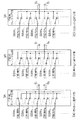
ここで、行配線セレクタ回路5は、例えば、図5に示す構成をしている。
また、図5における基準容量R0は、正確な容量値Crefが判明しており、交差部の容量の測定の基準となる容量負荷であり、例えば、行配線に近い値(同様な値)に設定されている。
行配線セレクタ回路5は、基準容量R0に接続されたスイッチSW0と、行配線群3における行配線R1,R2,R3,R4,…各々に対応したスイッチSW1,SW2,SW3,SW4,…を有している。出力端子S1は差動検出回路6の負入力端子IN(−)に接続され、出力端子S2は差動検出回路6の正入力端子IN(+)に接続されている。
Here, the row
Further, the reference capacitance R0 in FIG. 5 is a capacitance load that is known as an accurate capacitance value Cref and is a reference for measuring the capacitance at the intersection, and is set to a value close to the row wiring (similar value), for example. Has been.
The row
この行配線セレクタ回路5において、スイッチSW0は、基準容量R0を出力端子S1に対して接続する(接続状態)か、フローティング状態(非接続状態)とするかの切り替え(スイッチング)を行う。
また、スイッチSW1,SW2,SW3,SW4,…各々は、それぞれ行配線R1,R2,R3,R4,…を、フローティング状態とするか、または出力端子S1と接続するか、あるいは出力単位S2と接続するかの切り替え(スイッチング)を行う。
タイミング制御回路9は、行配線群3の行配線から隣接する2つの行配線を順次選択(測定する行配線の対として選択)し、スイッチSW0,SW1,SW2,SW3,SW4,…各々を、出力端子S1または出力端子S2のいずれかに、時系列に接続する切り替え信号を、行配線セレクタ回路5へ出力する。
In the row
Further, each of the switches SW1, SW2, SW3, SW4,... Makes the row wirings R1, R2, R3, R4,... Floating or connected to the output terminal S1, or connected to the output unit S2. Switching between switching (switching).
The
次に、図6を参照し、図1における差動検出回路6の説明を行う。図6は、差動増幅回路6の一構成例を示すブロック図である。
差動増幅回路6は差動増幅器121,122,123が設けられており、入力端子IN(−)及びIN(+)から入力される、交差部の容量に対応して流れる各々電流を電圧に変換して、この電圧の差分値を出力する。
ここで、差動増幅器121の反転入力端子は入力端子IN(−)に接続され、差動増幅器122の反転入力端子は入力端子IN(+)に接続され、差動増幅器121及び122の非反転入力端子には所定の基準電位が供給されている。
Next, the
The
Here, the inverting input terminal of the
差動増幅器121は、入力端子IN(−)から入力される電流を電圧に変換するものであり、反転入力端子と出力端子との間に、帰還容量125と、この帰還容量125の電荷を放電させるためのアナログスイッチ124とが並列に接続されている。
同様に、差動増幅器122は、入力端子IN(+)から入力される電流を電圧に変換するものであり、反転入力端子と出力端子の間に接続された帰還容量127と、この帰還容量127の電荷を放電させるためのアナログスイッチ126とが並列に接続されている。ここで、容量125と容量127とは、同様の容量値Cfを有している。
The
Similarly, the
差動増幅器121の出力端子は抵抗128を介して差動増幅器123の反転入力端子に接続され、差動増幅器122の出力端子は抵抗129を介して差動増幅器123の非反転入力端子に接続されている。
また、差動増幅器123は、非反転入力端子が抵抗130を介して基準電位に接続されており、反転入力端子が抵抗131を介して出力端子に接続されている。これにより、差動増幅器123は、抵抗128,129,130,131により設定された増幅度により、差動増幅器121と差動増幅器122との出力電圧の差分値の増幅を行う。
The output terminal of the
The
次に、上記構成からなる、本発明の第1の実施形態に係る容量検出回路100の動作例を、図1を参照して説明する。
復号演算回路10が外部から容量検出の開始、すなわち指紋センサ(センサ部1)での指紋の採取を行う信号が入力されたとする。
これにより、復号演算回路10は、タイミング制御回路9に対して、検出開始を指示する開始信号を出力する。次に、タイミング制御回路9は、行配線セレクタ回路5に、順次、切り替え信号を出力する。
そして、行配線セレクタ回路5は、時系列に入力される上記切り替え信号により、順次、内部各スイッチの切り替えを行う(各時刻から開始される測定に対応させる)。
Next, an operation example of the
It is assumed that the
Thereby, the
Then, the row
図5(a)に示すように、時刻t1において(時刻t1から開始される測定において)、基準となる電圧レベルを設定するため、タイミング制御回路9は、スイッチSW0により、既知である容量値Crefの基準容量R0を出力端子S1に接続し、スイッチSW1により、行配線R1を出力端子S2へ接続し、他のスイッチSW3,SW4,…をフローティング状態とする切り替え信号を行配線セレクタ回路5へ出力する。
これにより、行配線セレクタ回路5は、スイッチSW0により基準容量R0を出力端子S1に接続し、スイッチSW1により行配線R1を出力端子S2へ接続し、他のスイッチSW3,SW4,…をフローティング状態とする。
そして、タイミング制御回路9は、差動検出回路6及び列配線駆動部4に対してリセットを供給し、この差動増幅回路6と列配線駆動部4とを初期化し、基準容量R0及び行配線R1の電位を等しくし、列配線駆動部4がクロックの入力に同期して、列配線群2における列配線C1に駆動パルスを出力するよう初期設定を行う。ここで、図示しないが、列配線群2は、列配線C1,C2,…の複数の列配線から構成され、測定において順次選択されて駆動パルスが出力される。
As shown in FIG. 5A, in order to set a reference voltage level at time t1 (in measurement starting from time t1), the
Thereby, the row
Then, the
次に、タイミング制御回路9は、列配線駆動部4に対してクロックを出力し、列配線を駆動する駆動パルスを出力させる(Hレベルに立ち上げる)。
これにより、列配線駆動部4は、列配線群2における列配線C1に対して、上記クロックに同期して、駆動パルスを出力する。
そして、差動増幅回路6は、印加された上記駆動パルスの電圧レベルにより、基準容量R0と、列配線C1及び行配線R1との交差部との各々の容量に対応して、入力端子IN(−)及びIN(+)に流れる電流を電圧に変換して、これらの差分値をとり、測定電圧として出力する。
Next, the
Thereby, the column
Then, the
次に、タイミング制御回路9は、駆動パルスの印加から所定の時間が経過した後、サンプルホールド回路7にサンプルホールド(S/H)信号を出力する。
これにより、サンプルホールド回路7は、入力される上記サンプルホールド信号に同期して、差動増幅回路6の出力している電圧レベルを一時的に保持し(電圧情報として記憶し)、この電圧レベルと同一の電圧レベルの信号を、A/D変換器8に対して出力する。
そして、列配線駆動部4は、サンプルホールド信号に同期して、駆動パルスの出力を停止する(Lレベルに立ち下げ)。
次に、タイミング制御回路9は、サンプルホールド信号を出力し、所定の時間が過した後、演算制御回路10に変換信号を出力する。
Next, the
Thereby, the
Then, the column
Next, the
そして、演算制御回路10は、上記変換信号に同期して、A/D変換器8に対してA/Dクロックを出力する。
これにより、A/D変換器8は、上記A/Dクロックに同期して、サンプルホールド回路7から入力されている電圧レベルを、デジタルデータの測定データに変換し、この測定データを演算制御回路10へ出力する。
このときの測定データは、
d1=V1−Vref+Vofs
である。ここで、V1は入力端子IN(+)に入力される行配線R1に流れる電流を電圧に変換した値であり、Vrefは基準容量に流れる電流を電圧に変換した値であり、Vofs出力データを符号ビットなしの8ビット値(ビット数は任意)で表すためのオフセット値である。
The
As a result, the A / D converter 8 converts the voltage level input from the
The measurement data at this time is
d1 = V1-Vref + Vofs
It is. Here, V1 is a value obtained by converting the current flowing through the row wiring R1 inputted to the input terminal IN (+) into a voltage, Vref is a value obtained by converting the current flowing through the reference capacitor into a voltage, and Vofs output data is expressed as Vofs output data. This is an offset value for representing an 8-bit value (the number of bits is arbitrary) without a sign bit.
次に、図5(b)に示すように、時刻t2において(時刻t2から開始される測定において)、次の行配線対(隣接する2本の行配線の組)の測定を行うために、タイミング制御回路9は、スイッチSW1により、行配線R1を出力端子S1に接続し、スイッチSW2により、行配線R2を出力端子S2へ接続し、その他のスイッチSW0,SW3,SW4,…をフローティング状態とする切り替え信号を行配線セレクタ回路5へ出力する。
これにより、行配線セレクタ回路5は、スイッチSW1により、行配線R1を出力端子S1に接続し、スイッチSW2により、行配線R2を出力端子S2へ接続し、その他のスイッチSW0,SW3,SW4,…をフローティング状態とする。
そして、タイミング制御回路9は、差動検出回路6に対してリセットを供給し、この差動増幅回路6を初期化し、行配線R1,R2の電位を等しくする。
Next, as shown in FIG. 5B, at the time t2 (in the measurement starting from the time t2), in order to perform the measurement of the next row wiring pair (a set of two adjacent row wirings), The
Accordingly, the row
Then, the
次に、タイミング制御回路9は、列配線駆動部4に対してクロックを出力し、列配線を駆動する駆動パルスを出力させる。
これにより、列配線駆動部4は、列配線群2における列配線C1に対して、上記クロックに同期して、駆動パルスを出力する。
そして、差動増幅回路6は、印加された上記駆動パルスの電圧レベルにより、列配線C1及び行配線R1との交差部と、列配線C1及び行配線R2との交差部との各々の容量に対応して、入力端子IN(−)及びIN(+)に流れる電流を電圧に変換して、これらの差分値をとり、測定電圧として出力する。
Next, the
Thereby, the column
Then, the
次に、タイミング制御回路9は、駆動パルスの印加から所定の時間が経過した後、サンプルホールド回路7にサンプルホールド信号を出力する。
これにより、サンプルホールド回路7は、入力される上記サンプルホールド信号に同期して、差動増幅回路6の出力している電圧レベルを一時的に保持し、この電圧レベルと同一の電圧レベルの信号を、A/D変換器8に対して出力する。
そして、列配線駆動部4は、サンプルホールド信号に同期して、駆動パルスの出力を停止する。
次に、タイミング制御回路9は、サンプルホールド信号を出力し、所定の時間が経過した後、演算制御回路10に変換信号を出力する。
Next, the
Accordingly, the
Then, the column
Next, the
そして、演算制御回路10は、上記変換信号に同期して、A/D変換器8に対してA/Dクロックを出力する。
これにより、A/D変換器8は、上記A/Dクロックに同期して、サンプルホールド回路7から入力されている電圧レベルを、デジタルデータの測定データに変換し、この測定データを演算制御回路10へ出力する。
このときの測定データは、
d2=V2−V1+Vofs
である。ここで、V2は入力端子IN(+)に入力される行配線R2に流れる電流を電圧に変換した値である。
The
As a result, the A / D converter 8 converts the voltage level input from the
The measurement data at this time is
d2 = V2-V1 + Vofs
It is. Here, V2 is a value obtained by converting a current flowing in the row wiring R2 input to the input terminal IN (+) into a voltage.
同様に、図5(c)に示すように、時刻t3において(時刻t3から開始される測定において)、次の行配線対の測定を行うために、タイミング制御回路9は、スイッチSW2により、行配線R2を出力端子S1に接続し、スイッチSW3により、行配線R3を出力端子S2へ接続し、その他のスイッチSW0,SW1,SW4,…をフローティング状態とする切り替え信号を行配線セレクタ回路5へ出力する。
これにより、行配線セレクタ回路5は、スイッチSW2により、行配線R2を出力端子S1に接続し、スイッチSW3により、行配線R3を出力端子S2へ接続し、その他のスイッチSW0,SW1,SW4,…をフローティング状態とする。
そして、タイミング制御回路9は、差動検出回路6に対してリセットを供給し、この差動増幅回路6を初期化し、行配線R2,R3の電位を等しくする。
Similarly, as shown in FIG. 5C, at the time t3 (in the measurement started from the time t3), the
Thereby, the row
The
後の処理は、測定対象として選択される隣接する行配線対が行配線R2,R3になっただけで、時刻t2と同様の測定処理が行われる。
そして、A/D変換器8は、上記A/Dクロックに同期して、サンプルホールド回路7から入力されている電圧レベルを、デジタルデータの測定データに変換し、この測定データを演算制御回路10へ出力する。
このときの測定データは、
d3=V3−V2+Vofs
である。ここで、V3は入力端子IN(+)に入力される行配線R3に流れる電流を電圧に変換した値である。
In the subsequent processing, the measurement processing similar to that at time t2 is performed only when the adjacent row wiring pair selected as the measurement target becomes the row wiring R2, R3.
The A / D converter 8 converts the voltage level input from the
The measurement data at this time is
d3 = V3-V2 + Vofs
It is. Here, V3 is a value obtained by converting a current flowing in the row wiring R3 input to the input terminal IN (+) into a voltage.
そして、上述した処理を行配線群3の行配線が全て行配線対として測定されるまで、すなわち行配線群3が行配線R1〜Rnのn本で構成されているとすると、基準容量R0と行配線R1の行配線対から測定が開始され、行配線Rn-1と行配線Rnの行配線対の測定まで、各行配線対の測定において列配線C1が駆動パルスにより活性化されて測定が行われる。
これにより、演算制御回路10には、列配線C1と、行配線R1〜Rnとにおける各交差部の容量に対応した測定データd1〜dnが、列配線C1に対応して記憶されている。
Then, if the above-described processing is performed until all the row wirings in the
As a result, the
列配線群2が15本の列配線から構成されているとすると、上記処理を列配線群2における他の列配線C2〜C15においても、基準容量R0,行配線R1〜Rnにおける隣接する行配線対の測定を行い、各列配線に対応する測定データを得、演算制御回路10に各列配線に対応して記憶される。
ここで、行配線セレクタ回路5は、基準容量R0,行配線R1〜Rnにおける隣接する行配線対の形成が全て終了すると、すなわち、行配線Rn-1と行配線Rnとの行配線対の形成時にタイミング制御回路9に対して、行配線対終了を示す信号を出力する。
Assuming that the
Here, the row
そして、タイミング制御回路9は、行配線対終了を示す上記信号が入力されると、次の列配線駆動部4に対するクロックの前に、列配線駆動部4が、次から列配線C2に対して駆動パルスを出力するように設定を変更する制御信号を出力する。
これにより、タイミング制御回路9は、次にクロックが入力されると、このクロックに同期して、行配線群3における行配線対の組み合わせを変更しつつ、列配線C1を駆動したときと同様に、列配線C2に対して駆動パルスを出力し、列配線C1と各行配線との交差部の容量測定を行う。
このように、演算制御回路10は、列配線群2における全ての列配線に渡り、順次、列配線を駆動することで、基準容量及び行配線群3における行配線対での容量測定が終了すると、得られた測定データから、各交差部の容量に対応した電圧データを求める演算を行う。
When the signal indicating the end of the row wiring pair is input to the
Thus, when the clock is next input, the
As described above, the
ここで、演算制御回路10は、得られた測定データを、列配線毎に累積的に加算していくことにより、各列配線と行配線との各交差部の容量に対応した電圧データを求めることが出来る。
例えば、列配線C1における各行配線との交差部の容量に対応する演算を行う。
演算制御回路10は、基準容量Crefに対応した電圧データをdr(すなわちVref)とし、列配線C1と行配線R1との交差部の容量に対応する測定データをd1(時刻t1における測定データ、すなわち時刻t1から開始される測定での測定データ)とし、求めるこの交差部の電圧データをds1とすると、電圧データds1は
ds1=d1+dr=V1−Vref+Vofs+Vref=V1+Vofs
Here, the
For example, an operation corresponding to the capacitance at the intersection of the column wiring C1 with each row wiring is performed.
The
また、同様に、列配線C1と行配線R2,R3との交差部の容量に対応する測定データを各々d2,d3とするとし、求める各々の交差部の電圧データをds2,ds3とすると、
ds2=d2+ds1=V2−V1+V1+Vofs=V2+Vofs
ds3=d3+ds2=V3−V2+V2+Vofs=V3+Vofs
と、順次、測定データを累積加算することにより、各交差部の容量に対応した電圧値を得ることができる。
Similarly, if the measurement data corresponding to the capacitance at the intersection between the column wiring C1 and the row wirings R2 and R3 are d2 and d3, respectively, and the voltage data at each intersection to be obtained is ds2 and ds3,
ds2 = d2 + ds1 = V2-V1 + V1 + Vofs = V2 + Vofs
ds3 = d3 + ds2 = V3-V2 + V2 + Vofs = V3 + Vofs
Then, by sequentially accumulating the measurement data, a voltage value corresponding to the capacity of each intersection can be obtained.
次に、上述した測定においては、駆動パルスの立ち上がり(第2の電圧から第1の電圧への遷移;第1の電圧>第2の電圧)における容量測定のみを行っているが、駆動パルスの立ち上がり及び立ち下がり(第1の電圧から第2の電圧への遷移における測定を行うことにより、時間的差動演算により不要なオフセットが除去することができ、計算制度を向上させることができる。
すなわち、上述した駆動パルスの立ち上がりのみ用いた測定においては、図7に示すように、出力OUTが基準電位から下降する場合も、上昇する場合も、アナログスイッチ124(または126)のフィードスルー電流によるオフセットVkが+方向に発生する。図7は、差動増幅器121(または122)の動作を示す波形図である。この実施形態のように、検出対象の交差部の容量値が数十から数百フェムトファラッドの場合はこのフィードスルーによるオフセットを無視できない。
Next, in the above-described measurement, only the capacitance measurement at the rising edge of the drive pulse (transition from the second voltage to the first voltage; the first voltage> the second voltage) is performed. Rising and falling (by measuring at the transition from the first voltage to the second voltage, unnecessary offset can be removed by temporal differential calculation, and the calculation system can be improved.
In other words, in the measurement using only the rising edge of the drive pulse described above, as shown in FIG. 7, the output OUT depends on the feedthrough current of the analog switch 124 (or 126), whether it falls or rises from the reference potential. An offset Vk occurs in the + direction. FIG. 7 is a waveform diagram showing the operation of the differential amplifier 121 (or 122). As in this embodiment, when the capacitance value of the intersection to be detected is tens to hundreds of femtofarads, the offset due to this feedthrough cannot be ignored.
上記の基準容量R0の測定において、(差動増幅器121における測定)
−Vuref0=−Vuref+Vka
が検出対象の交差部の容量値に比例する電圧となるが、測定される電圧はVurefであり、この電圧Vurefにはオフセットによる誤差Vkが含まれてしまう。
Vuref=Vuref0+Vka
そこで、この実施形態においては、検出対象容量Csの放電時の電圧Vd1も測定する。ここで、電圧Vd10が以下に示すように、
Vdref0=Vdref−Vka
が容量Csに比例する電圧であり、測定される電圧は
Vdref=Vdref0+Vka
となる。
In the measurement of the reference capacitance R0 (measurement in the differential amplifier 121)
-Vuref0 = -Vuref + Vka
Becomes a voltage proportional to the capacitance value of the crossing portion to be detected, but the measured voltage is Vuref, and this voltage Vuref includes an error Vk due to an offset.
Vuref = Vuref0 + Vka
Therefore, in this embodiment, the voltage Vd1 at the time of discharging the detection target capacitor Cs is also measured. Here, the voltage Vd10 is as follows:
Vdref0 = Vdref-Vka
Is a voltage proportional to the capacitance Cs, and the measured voltage is Vdref = Vdref0 + Vka
It becomes.
同様に、行配線R1の測定において、(差動増幅器122における測定)
−Vu10=−Vu1+Vkb
が検出対象の交差部の容量値に比例する電圧となるが、測定される電圧はVu1であり、この電圧Vu1にはオフセットによる誤差Vkが含まれてしまう。
Vu1=Vu10+Vkb
そこで、この実施形態においては、検出対象容量Csの放電時の電圧Vd1も測定する。ここで、電圧Vd10が以下に示すように、
Vd10=Vd1−Vkb
が容量Csに比例する電圧であり、測定される電圧は
Vd1=Vd10+Vkb
となる。
Similarly, in the measurement of the row wiring R1, (measurement in the differential amplifier 122)
-Vu10 = -Vu1 + Vkb
Becomes a voltage proportional to the capacitance value of the intersection of the detection target, but the measured voltage is Vu1, and this voltage Vu1 includes an error Vk due to an offset.
Vu1 = Vu10 + Vkb
Therefore, in this embodiment, the voltage Vd1 at the time of discharging the detection target capacitor Cs is also measured. Here, the voltage Vd10 is as follows:
Vd10 = Vd1-Vkb
Is a voltage proportional to the capacitance Cs, and the measured voltage is Vd1 = Vd10 + Vkb
It becomes.
そして、差動検出回路6は、駆動パルスの立ち上がり時には、増幅度を「1」とすると
Vsu1=Vu1−Vuref+Vof
=Vu10+Vkb−(Vuref0+Vka)+Vof
=Vu10−Vuref0+Vkb−Vka+Vof
となる。VofはA/D変換器8におけるオフセット成分である。
同様に、差動検出回路6は、駆動パルスの立ち下がり時には、
Vsd1=Vd1−Vdref+Vof
=Vd10+Vkb−(Vdref0+Vka)+Vof
=Vd10−Vdref0+Vkb−Vka+Vof
と求められる。
The
= Vu10 + Vkb- (Vuref0 + Vka) + Vof
= Vu10-Vuref0 + Vkb-Vka + Vof
It becomes. Vof is an offset component in the A / D converter 8.
Similarly, the
Vsd1 = Vd1−Vdref + Vof
= Vd10 + Vkb- (Vdref0 + Vka) + Vof
= Vd10-Vdref0 + Vkb-Vka + Vof
Is required.
これらの測定電圧Vsu1及びVsd1が順次サンプルホールド回路7において保持され、次いでホールドされた電圧を、A/D変換器8により各々測定電圧毎に、測定データdsu1及びdsd1にA/D(アナログ/デジタル)変換し、復号演算回路10内のメモリに記憶させる。
そして、復号演算回路10において、
d1=dsd1−dsu1+Vofs
=(Vd10−Vdref0+Vkb−Vka+Vof)
−(Vu10−Vuref0+Vkb−Vka+Vof)+Vofs
=Vd10−Vu10−(Vdref0−Vuref0)+Vofs
となる演算を行い、これにより、フィードスルー電流によるオフセット誤差及びA/D変換器8における変換時のオフセットVofを含まない測定値測定データdを得ることができる(ここで、Vofsは、出力データを符号ビットなしの8ビット値(ビット数は任意)で満たすためのオフセット値)。
以降の各交差部の容量に対応した電圧データdsを求める処理は、すでに述べた累積加算を行う方法と同様である。
上述の説明において、容量検出回路100が、検出処理により得られた測定データを一時的に保持し、全ての列配線に渡り容量測定が終了した後に、センサ部1における各交差部の容量に対応させて電圧データを求める演算を行うように記述した。しかしながら、容量検出回路100が、得られた測定データを随時累積加算して、容量検出の動作と並行して(ほぼ同時に)電圧データを求める演算を行うようにしてもよい。
These measurement voltages Vsu1 and Vsd1 are sequentially held in the sample-and-
In the
d1 = dsd1-dsu1 + Vofs
= (Vd10-Vdref0 + Vkb-Vka + Vof)
-(Vu10-Vuref0 + Vkb-Vka + Vof) + Vofs
= Vd10-Vu10- (Vdref0-Vuref0) + Vofs
Thus, measurement value measurement data d that does not include the offset error due to the feedthrough current and the offset Vof at the time of conversion in the A / D converter 8 can be obtained (where Vofs is the output data). ) With an 8-bit value without a sign bit (the number of bits is arbitrary).
The subsequent processing for obtaining the voltage data ds corresponding to the capacitance of each intersection is the same as the method of performing cumulative addition described above.
In the above description, the
本発明の第2の実施形態による容量検出回路を図8を参照して説明する。図8は、第2の実施形態による容量検出回路の一構成例を示すブロック図である。この図において、図1に示す第1の実施形態の容量検出器回路100と同一の部分には同一の符号を付し、その説明を省略する。この図8に示す容量検出器回路200が、図1に示す第1の実施形態と異なる点は、行配列セレクタ5がM個の行配列セレクタ(51〜5M)に分割されている点である。
A capacitance detection circuit according to a second embodiment of the present invention will be described with reference to FIG. FIG. 8 is a block diagram illustrating a configuration example of the capacitance detection circuit according to the second embodiment. In this figure, the same parts as those of the
すなわち、行配線群3の行配線R1〜RnがM分割され、行配列セレクタ51〜5M各々は、それぞれ「n/M」本の列配線が行配線ブロックとして制御対象として対応づけられている。
このため、行配列セレクタ51〜5M各々に、差動検出回路61,62,…,6M、及びサンプルホールド回路71〜7Mがそれぞれ対応している。
また、後段セレクタ回路11は、サンプルホールド回路71〜7Mのいずれの保持している電圧レベルをデジタルデータに変換(A/D変換)するかの切り替えを行う。
That is, the row wirings R1 to Rn of the
Therefore, the
Further, the
そして、タイミング制御回路9は、行配線セレクタ回路51〜5Mの切り替えに対応して、後段セレクタ回路11に対して、切り替え信号を出力する。
ここで、第2の実施形態においては、行配線セレクタ51〜5M毎に、第1の実施形態と同様な測定、すなわち、基準容量R0との行配線対間の電圧の差分値の測定、及び各行配線セレクタ内の隣接する行配線対間の差分値の測定が行われる。
タイミング制御回路9は、行配線セレクタ51〜5M各々の行配線対を設定するための切り替え信号だけでなく、各行配線セレクタに対応する行配線ブロックの全ての行配線における容量測定が終了した後、順次、次の行配線セレクタの行配線ブロックに切り替える切り替え信号を出力する。
ここで、第1の実施形態と同様に、容量検出回路100が、上述した処理により得られた測定データを一時的に保持し、全ての列配線に渡り容量測定が終了した後に、センサ部1における各交差部の容量に対応させて電圧データを求める演算を行っても良いし、また、容量検出回路100が、得られた測定データを随時累積加算して、容量検出の動作と並行して(ほぼ同時に)電圧データを求める演算を行うようにしてもよい。
The
Here, in the second embodiment, for each of the
The
Here, as in the first embodiment, after the
そして、行配線対の測定の終了後に、第1の実施形態と同様に、演算制御回路10が累積加算による各交差部の容量に対応する電圧データを求めるが、この第2の実施形態においては各行配線セレクタ単位に累積加算を行うため、累積加算の繰り返し回数(各列配線ブロック毎における累積数が行配線群3全体の場合に比較して)を、第1の実施形態の1/Mに減少させることができ、誤差の累積を削減することができる。
また、上記構成により、差動検出回路61〜6Mの入力端子IN(+),IN(−)に入力される行配線数を、行配線ブロックとして再構成して削減したため、差動検出回路6の応答速度及び検出感度の向上が期待できる。
Then, after the measurement of the row wiring pair, as in the first embodiment, the arithmetic and
Further, with the above configuration, the number of row wirings input to the input terminals IN (+) and IN (−) of the
本発明の第3の実施形態による容量検出回路を図9を参照して説明する。図9は、第3の実施形態による容量検出回路の一構成例を示すブロック図である。この図において、図1に示す第1の実施形態の容量検出器回路100と同一の部分には同一の符号を付し、その説明を省略する。この図9に示す容量検出器回路300が、図1に示す第1の実施形態と異なる点は、第1の実施形態において、基準容量R0を設けて基準の測定電圧として、以降の測定データの累積加算の基準のデータに用いていたが、第3の実施形態においては、特に基準容量を設けずに、行配線群3における測定対象の行配線以外の行配線を接続して参照容量として、各行配線の容量の加算値、すなわち各行配線に流れる電流の加算値(混合値)を、参照容量(基準とする容量)に流れる電流値として各行配線の容量の算出に使用することにある。これは、複数の行配線に流れる電流値を平均すると、ほぼ同様の電流値になることを利用している。
A capacitance detection circuit according to a third embodiment of the present invention will be described with reference to FIG. FIG. 9 is a block diagram illustrating a configuration example of the capacitance detection circuit according to the third embodiment. In this figure, the same parts as those of the
ここで、行配線セレクタ回路5Aは、図10に示すように、タイミング制御回路9により制御される、スイッチSSW1〜SSW5,…を有しており、行配線群3の各行配線各々を、出力端子S1,S2のいずれかに接続する。
すなわち、スイッチSSW1〜SSW5,…各々は、タイミング制御回路1の制御により、それぞれ行配線R1〜R5,…に対応して設けられており、各行配線を出力端子S1またはS2のいずれかに接続する。
また、図6の差動検出回路6(第1の実施形態)と、図11の差動検出回路6A,初段C-V変換回路6B,6Cとは構成が同様であるが、差動増幅器121の帰還容量である容量150と差動増幅器122の帰還容量である容量127との容量値の関係が異なる。図11において、図6と同様の構成には同一の符号を付し、説明を省略する。
初段C-V変換回路6Bは図6の差動検出回路6の入力端子IN(−)に接続された変換回路に対応し、初段C-V変換回路6Cは図6の差動検出回路6の入力端子IN(+)に接続された変換回路に対応している。
Here, as shown in FIG. 10, the row
That is, the switches SSW1 to SSW5,... Are respectively provided corresponding to the row wirings R1 to R5,... Under the control of the
Further, the differential detection circuit 6 (first embodiment) of FIG. 6 and the
The first stage
容量150の容量値Cfrと容量127の容量値Cfとの関係は、参照容量として測定対象の行配線以外を全て接続して用いるため、測定対象の容量に流れる電流と、参照容量に流れる電流との測定のバランスを取るため、行配線群3がn本の行配線から構成されているとすると、
Cfr≒(n−1)・Cf
と設定し、(n−1)本の電流の総和を取ることによる容量150の電圧の増加を、容量127の電圧レベルと同等の値に調整して、測定電圧の参照に用いる電圧に制御することができる。
Since the relationship between the capacitance value Cfr of the
Cfr ≒ (n-1) ・ Cf
And the increase in the voltage of the
次に、上記構成からなる、本発明の第3の実施形態に係る容量検出回路の動作例を、図9を参照して説明する。
復号演算回路10が外部から容量検出の開始、すなわち指紋センサ(センサ部1)での指紋の採取を行う信号が入力されたとする。
これにより、演算制御回路10は、タイミング制御回路9に対して、検出開始を指示する開始信号を出力する。次に、タイミング制御回路9は、行配線セレクタ回路5Aに、順次、切り替え信号を出力する。
そして、行配線セレクタ回路5Aは、時系列に入力される上記切り替え信号により、順次、内部各スイッチの切り替えを行う。
Next, an operation example of the capacitance detection circuit according to the third embodiment of the present invention configured as described above will be described with reference to FIG.
It is assumed that the
As a result, the
The row
図10(a)に示すように、時刻t1において、測定対象の行配線として行配線R1を設定すると、タイミング制御回路9は、スイッチSSW1により、行配線R1を出力端子S2へ接続し、スイッチSSW2〜SSW5,…各々により、行配線群3の行配線R2〜R5を含む他の行配線を出力端子S1へ接続する切り替え信号を行配線セレクタ回路5Aへ出力する。
これにより、行配線セレクタ回路5Aは、測定対象の列配線R1をスイッチSSW1により出力端子S2へ接続し、参照容量として電流を加算する列配線R2〜R5を含む他の行配線を出力端子S1接続する。
そして、タイミング制御回路9は、初段C-V変換回路6B,6C及び列配線駆動部4に対してリセットを供給し、この初段C-V変換回路6B,6Cと列配線駆動部4とを初期化し、行配線R1〜R5,…の電位を等しくし、列配線駆動部4がクロックの入力に同期して、列配線C1に駆動パルスを出力するよう初期設定をを行う。
As shown in FIG. 10A, when the row wiring R1 is set as the row wiring to be measured at time t1, the
Thereby, the row
Then, the
次に、タイミング制御回路9は、列配線駆動部4に対してクロックを出力し、列配線を駆動する駆動パルスを出力させる(Hレベルに立ち上げる)。
これにより、列配線駆動部4は、列配線群2における列配線C1に対して、上記クロックに同期して、駆動パルスを出力する。
そして、初段C-V変換回路6B,6C各々は、印加された上記駆動パルスの電圧レベルにより、列配線C1と行配線R1と、列配線C1及び行配線分3の行配線R1以外の行配線との交差部との各々の容量に対応して、入力端子IN(−)及びIN(+)に流れる電流を電圧に変換して、差動増幅回路6Aは、これらの差分値をとり、測定電圧として出力する。
Next, the
Thereby, the column
Then, each of the first-stage
次に、タイミング制御回路9は、駆動パルスの印加から所定の時間が経過した後、サンプルホールド回路7にサンプルホールド(S/H)信号を出力する。
これにより、サンプルホールド回路7は、入力される上記サンプルホールド信号に同期して、差動増幅回路6Aの出力している電圧レベルを一時的に保持し(電圧情報として記憶し)、この電圧レベルと同一の電圧レベルの信号を、A/D変換器8に対して出力する。
そして、列配線駆動部4は、サンプルホールド信号に同期して、駆動パルスの出力を停止する(Lレベルに立ち下げ)。
次に、タイミング制御回路9は、サンプルホールド信号を出力し、所定の時間が過した後、演算制御回路10に変換信号を出力する。
Next, the
Accordingly, the
Then, the column
Next, the
そして、演算制御回路10は、上記変換信号に同期して、A/D変換器8に対してA/Dクロックを出力する。
これにより、A/D変換器8は、上記A/Dクロックに同期して、サンプルホールド回路7から入力されている電圧レベルを、デジタルデータの測定データに変換し、この測定データを演算制御回路10へ出力する。
このときの測定データは、
d1=V1−Vr1+Vofs
である。ここで、V1は入力端子IN(+)に入力される行配線R1に流れる電流を電圧に変換した値であり、Vr1は行配線群3における行配線R1以外の行配線に流れる電流を電圧に変換した参照値であり、Vofsは出力データを符号ビットなしの8ビット値(ビット数は任意)で表すためのオフセット値である。
The
As a result, the A / D converter 8 converts the voltage level input from the
The measurement data at this time is
d1 = V1-Vr1 + Vofs
It is. Here, V1 is a value obtained by converting the current flowing in the row wiring R1 input to the input terminal IN (+) into a voltage, and Vr1 is the voltage flowing in the row wiring other than the row wiring R1 in the
次に、図10(b)に示すように、時刻t2において、次の行配線R2における交差部の測定を行うため、タイミング制御回路9は、スイッチSSW2により、行配線R2を出力端子S2に接続し、スイッチSSW1,SSW3〜SSW5,…各々により、列配線群3における行配線R2以外の行配線全てを出力端子S1へ接続する切り替え信号を行配線セレクタ回路5Aへ出力する。
これにより、行配線セレクタ回路5Aは、スイッチSSW2により、行配線R2を出力端子S2に接続し、スイッチSSW1,SSW3〜SSW5,…各々により、列配線群3における行配線R2以外の行配線全てをを出力端子S1へ接続する。
そして、タイミング制御回路9は、初段C-V変換回路6B,6Cに対してリセットを供給し、この初段C-V変換回路6B,6Cを初期化し、行配線R1〜R5,…の電位を等しくする。
Next, as shown in FIG. 10B, at time t2, in order to measure the intersection of the next row wiring R2, the
Thereby, the row
Then, the
次に、タイミング制御回路9は、列配線駆動部4に対してクロックを出力し、列配線を駆動する駆動パルスを出力させる。
これにより、列配線駆動部4は、列配線群2における列配線C1に対して、上記クロックに同期して、駆動パルスを出力する。
そして、初段C-V変換回路6B,6C各々は、印加された上記駆動パルスの電圧レベルにより、列配線C1及び行配線R1との交差部と、列配線C1及び行配線R2との交差部との各々の容量に対応して、入力端子IN(−)及びIN(+)に流れる電流を電圧に変換して、差動検出回路6Aはこれらの差分値をとり、測定電圧として出力する。
Next, the
Thereby, the column
Then, each of the first-stage
次に、タイミング制御回路9は、駆動パルスの印加から所定の時間が経過した後、サンプルホールド回路7にサンプルホールド信号を出力する。
これにより、サンプルホールド回路7は、入力される上記サンプルホールド信号に同期して、差動増幅回路6Aの出力している電圧レベルを一時的に保持し、この電圧レベルと同一の電圧レベルの信号を、A/D変換器8に対して出力する。
そして、列配線駆動部4は、サンプルホールド信号に同期して、駆動パルスの出力を停止する。
次に、タイミング制御回路9は、サンプルホールド信号を出力し、所定の時間が過した後、演算制御回路10に変換信号を出力する。
Next, the
Accordingly, the
Then, the column
Next, the
そして、演算制御回路10は、上記変換信号に同期して、A/D変換器8に対してA/Dクロックを出力する。
これにより、A/D変換器8は、上記A/Dクロックに同期して、サンプルホールド回路7から入力されている電圧レベルを、デジタルデータの測定データに変換し、この測定データを演算制御回路10へ出力する。
このときの測定データは、
d2=V2−Vr2+Vofs
である。ここで、V2は入力端子IN(+)に入力される行配線R2に流れる電流を電圧に変換した値であり、Vr2は行配線群3における行配線R2以外の行配線に流れる電流を電圧に交換した参照値である。
The
As a result, the A / D converter 8 converts the voltage level input from the
The measurement data at this time is
d2 = V2-Vr2 + Vofs
It is. Here, V2 is a value obtained by converting the current flowing in the row wiring R2 input to the input terminal IN (+) into a voltage, and Vr2 is the voltage flowing in the row wiring other than the row wiring R2 in the
同様に、図10(c)に示すように、時刻t3において、次の行配線R3の測定を行うために、タイミング制御回路9は、スイッチSSW3により、行配線R3を出力端子S2に接続し、スイッチSSW1,SSW2,SSW4,SSW5,…各々により、行配線R1,R2,R4,R5,…それぞれを出力端子S1へ接続する切り替え信号を行配線セレクタ回路5Aへ出力する。
これにより、行配線セレクタ回路5Aは、スイッチSSW3により、行配線R3を出力端子S1に接続し、スイッチSSW1,SSW2,SSW4,SSW5,…各々により、行配線R1,R2,R4,R5,…それぞれを出力端子S2へ接続する。
そして、タイミング制御回路9は、初段C-V変換回路6B,6Cに対してリセットを供給し、初段C-V変換回路6B,6Cを初期化し、行配線R1〜R5,…の電位を等しくする。
Similarly, as shown in FIG. 10C, in order to measure the next row wiring R3 at time t3, the
Accordingly, the row
Then, the
後の処理は、測定対象が行配線R3になっただけで、時刻t2と同様の測定処理が行われる。
そして、A/D変換器8は、上記A/Dクロックに同期して、サンプルホールド回路7から入力されている電圧レベルを、デジタルデータの測定データに変換し、この測定データを演算制御回路10へ出力する。
このときの測定データは、
d3=V3−Vr3+Vofs
である。ここで、V3は入力端子IN(+)に入力される行配線R3に流れる電流を電圧に変換した値であり、Vr3は、行配線群3における行配線R3以外の行配線に流れる電流を電圧に変換した参照値である。
In the subsequent processing, the measurement processing similar to that at time t2 is performed only when the measurement target is the row wiring R3.
The A / D converter 8 converts the voltage level input from the
The measurement data at this time is
d3 = V3-Vr3 + Vofs
It is. Here, V3 is a value obtained by converting a current flowing in the row wiring R3 input to the input terminal IN (+) into a voltage, and Vr3 is a voltage flowing in a row wiring other than the row wiring R3 in the
そして、上述した処理を行配線群3の行配線が全て測定対象として測定されるまで、すなわち行配線群3が行配線R1〜Rnのn本で構成されているとすると、行配線R1から行配線Rnまでの各行配線の測定において列配線C1が駆動パルスにより活性化されて測定が行われる。
これにより、演算制御回路10には、列配線C1と、行配線R1〜Rnとにおける各交差部の容量に対応した測定データd1〜dnが、列配線C1に対応して記憶される。
Then, if the above-described processing is performed until all the row wirings in the
As a result, the
また、上述した各行配線の測定において、初段C-V変換回路6Bは、参照電圧V(j)として
Vr(j)=k・(Cr(j)/Cfr)
を出力する。ここで、Crは行配線群3における行配線R(j)を除いた(n−1)本の行配線の交差部の容量の総和であり、kは増幅度である。Cr(j)は、数多くの交差部の容量が平均化されたものであり、概略一定値となることが期待される。したがって、上述の式により求められる参照電圧Vr(j)も概略一定値となる。
また、初段C-V変換回路6Cは、測定電圧Vsとして
Vs=k・(Cs/Cf)
を出力する。ここで、Csは測定対象の行配線の交差部の容量であり、kは増幅度である。
そして、差動検出回路6Aは、測定電圧Vsから参照電圧Vr(j)を減算して得られる差分電圧Voutを新たな測定電圧としてサンプルホールド回路7へ出力する。
In the above-described measurement of each row wiring, the first-stage
Is output. Here, Cr is the sum of the capacitances of the intersections of (n−1) row wirings excluding the row wiring R (j) in the
The first-stage
Is output. Here, Cs is the capacitance at the intersection of the row wiring to be measured, and k is the amplification factor.
Then, the
この結果、演算制御回路10には、第1の実施形態と同様に、列配線毎に、各行配線における時系列の測定データdiが格納されていくことになる。
しかしながら、第3の実施形態においては、測定データdiが行配線毎に独立しているため、第1及び第2の実施形態と異なり、累積加算による各行配線の交差部の容量の算出が必要ない。
例えば、各交差部の測定データdiから電圧データdsを求める場合、測定データが
di=Vi−Vr1+Vofs
であるため、電圧データは
ds=di+dr=Vi−Vr1+Vref+Vofs≒Vi+Vofs
として求められる。ここで、基準データdrは、予め測定され、設定されているVref電圧であり、参照電圧Vr1に概略同じ値になるように設定される(すなわち、Vr1≒Vref)。
As a result, the
However, in the third embodiment, since the measurement data di is independent for each row wiring, unlike the first and second embodiments, it is not necessary to calculate the capacitance at the intersection of each row wiring by cumulative addition. .
For example, when the voltage data ds is obtained from the measurement data di at each intersection, the measurement data is di = Vi−Vr1 + Vofs.
Therefore, the voltage data is ds = di + dr = Vi−Vr1 + Vref + Vofs≈Vi + Vofs
As required. Here, the standard data dr is a Vref voltage that is measured and set in advance, and is set to be approximately the same value as the reference voltage Vr1 (that is, Vr1≈Vref).
また、第3の実施形態において、この図9に示す行配線セレクタ回路5Aを、図8に示すように、行配列セレクタ回路(5A1〜5AM)に分割して構成しても良い。
すなわち、行配線群3の行配線R1〜RnがM分割され、行配列セレクタ回路5A1〜5AM各々は、それぞれ「n/M」本の列配線が行配線ブロックとして制御対象として対応づけられている。
このため、行配列セレクタ回路5A1〜5AM各々に、初段C-V変換回路6B1〜6BM,6C1〜6CM及び差動検出回路6A1〜6AMと、サンプルホールド回路71〜7Mとがそれぞれ対応するよう構成する。
また、後段セレクタ回路11は、サンプルホールド回路71〜7Mのいずれの保持している電圧レベルをデジタルデータに変換(A/D変換)するかの切り替えを行う。
以下の測定データを得る処理は第2の実施形態と同様であり、得られた測定データから各交差部の容量に対応する電圧データdsの算出方法はすでに述べた通りである。
In the third embodiment, the row
That is, the row wirings R1 to Rn of the
For this reason, the row array selector circuits 5A1 to 5AM are configured to correspond to the first stage CV conversion circuits 6B1 to 6BM, 6C1 to 6CM, the differential detection circuits 6A1 to 6AM, and the sample hold circuits 71 to 7M, respectively. .
Further, the
The processing for obtaining the following measurement data is the same as in the second embodiment, and the calculation method of the voltage data ds corresponding to the capacitance of each intersection from the obtained measurement data is as described above.
なお、図1,8,9における処理部の機能を実現するためのプログラムをコンピュータ読み取り可能な記録媒体に記録して、この記録媒体に記録されたプログラムをコンピュータシステムに読み込ませ、実行することにより容量検出の処理を行ってもよい。なお、ここでいう「コンピュータシステム」とは、OSや周辺機器等のハードウェアを含むものとする。また、「コンピュータシステム」は、ホームページ提供環境(あるいは表示環境)を備えたWWWシステムも含むものとする。また、「コンピュータ読み取り可能な記録媒体」とは、フレキシブルディスク、光磁気ディスク、ROM、CD−ROM等の可搬媒体、コンピュータシステムに内蔵されるハードディスク等の記憶装置のことをいう。さらに「コンピュータ読み取り可能な記録媒体」とは、インターネット等のネットワークや電話回線等の通信回線を介してプログラムが送信された場合のサーバやクライアントとなるコンピュータシステム内部の揮発性メモリ(RAM)のように、一定時間プログラムを保持しているものも含むものとする。 Note that a program for realizing the functions of the processing units in FIGS. 1, 8, and 9 is recorded on a computer-readable recording medium, and the program recorded on the recording medium is read into a computer system and executed. A capacity detection process may be performed. The “computer system” here includes an OS and hardware such as peripheral devices. The “computer system” includes a WWW system having a homepage providing environment (or display environment). The “computer-readable recording medium” refers to a storage device such as a flexible medium, a magneto-optical disk, a portable medium such as a ROM and a CD-ROM, and a hard disk incorporated in a computer system. Further, the “computer-readable recording medium” refers to a volatile memory (RAM) in a computer system that becomes a server or a client when a program is transmitted via a network such as the Internet or a communication line such as a telephone line. In addition, those holding programs for a certain period of time are also included.
また、上記プログラムは、このプログラムを記憶装置等に格納したコンピュータシステムから、伝送媒体を介して、あるいは、伝送媒体中の伝送波により他のコンピュータシステムに伝送されてもよい。ここで、プログラムを伝送する「伝送媒体」は、インターネット等のネットワーク(通信網)や電話回線等の通信回線(通信線)のように情報を伝送する機能を有する媒体のことをいう。また、上記プログラムは、前述した機能の一部を実現するためのものであっても良い。さらに、前述した機能をコンピュータシステムにすでに記録されているプログラムとの組み合わせで実現できるもの、いわゆる差分ファイル(差分プログラム)であっても良い。 The program may be transmitted from a computer system storing the program in a storage device or the like to another computer system via a transmission medium or by a transmission wave in the transmission medium. Here, the “transmission medium” for transmitting the program refers to a medium having a function of transmitting information, such as a network (communication network) such as the Internet or a communication line (communication line) such as a telephone line. The program may be for realizing a part of the functions described above. Furthermore, what can implement | achieve the function mentioned above in combination with the program already recorded on the computer system, and what is called a difference file (difference program) may be sufficient.
1…センサ部
2…列配線群
3…行配線群
4…列配線駆動部
5,5A…行配線セレクタ回路
6,6A…差動検出回路
6B,6C…初段I-V変換回路
7…サンプルホールド回路
8…A/D変換器
9…タイミング制御回路
10…演算制御回路
50…基板
51…絶縁膜
52…空隙
54…フィルム
100,200,300…容量検出回路
121,122,123…差動増幅器
DESCRIPTION OF
Claims (9)
前記列配線を駆動させる列配線駆動手段と、
前記行配線は、基準容量が接続された行配線と、第1行の行配線〜第m(m≧2)行の行配線とからなり、前記基準容量が接続された行配線と前記第1行の行配線との行配線対から選択され、前記第(m−1)行の行配線と前記第m行の行配線との行配線対まで隣接する行配線対を順次選択して、前記選択した行配線対の2配線の前者を第1の行配線、後者を第2の行配線とする行配線選択手段と、
前記駆動された列配線の交差部の容量に対応して前記第1の行配線に流れる電流と、前記第2の行配線に流れる電流とに基づいて、前記交差部の容量を求める容量演算部とを有し、
前記容量演算部が、
前記第1及び第2の行配線に対応する各交差部の容量に対応する電流値を差動増幅し、差動電圧信号として出力する差動電圧出力手段と、
時系列に入力される前記差動電圧信号により、前記各交差部の容量に対応する電圧値を求める演算手段と
を有することを特徴とする容量検出回路。 It is a capacitance detection circuit that detects a change in capacitance at a crossing portion of a column wiring and a row wiring as a voltage value by intersecting a row wiring with respect to a plurality of column wirings,
Column wiring driving means for driving the column wiring;
The row wiring includes a row wiring to which a reference capacitor is connected and a row wiring from the first row to m-th (m ≧ 2) rows, and the row wiring to which the reference capacitance is connected and the first wiring A row wiring pair selected from the row wiring pair with the row wiring of the row, and sequentially selecting adjacent row wiring pairs up to the row wiring pair of the (m−1) th row wiring and the m-th row wiring; A row wiring selection means in which the former of the two wirings of the selected row wiring pair is the first row wiring and the latter is the second row wiring ;
A capacitance calculation unit that obtains the capacitance of the intersection based on the current flowing in the first row wiring and the current flowing in the second row wiring corresponding to the capacitance of the intersection of the driven column wiring It has a door,
The capacity calculator is
Differential voltage output means for differentially amplifying a current value corresponding to the capacitance of each intersection corresponding to the first and second row wirings and outputting the differential voltage signal;
Calculation means for obtaining a voltage value corresponding to the capacitance of each intersection by the differential voltage signal input in time series;
A capacitance detection circuit comprising:
第1の検出期間において、第1の行配線として前記基準容量が接続された配線と、第2の行配線として前記第1の行配線と隣接する行配線とを選択し、
第2の検出期間以降において、前記複数の行配線から隣接する行配線を、第1及び第2の行配線として選択し、
前記演算手段が時系列に入力される差電圧信号を累積的に加算演算して、前記各交差部の容量に対応する電圧値を求めることを特徴とする請求項1記載の容量検出回路。 The row wiring selection means is
In the first detection period, select a wiring the reference capacitance is connected as the first row line, and a row wiring adjacent to the first row line as the second row line,
After the second detection period, adjacent row wirings are selected as the first and second row wirings from the plurality of row wirings,
It said calculating means cumulatively adds calculating a difference voltage signal input to the time series, the capacitance detection circuit according to claim 1, wherein the determination of the voltage value corresponding to the capacitance of each intersection.
第2の検出期間以降において、前記第1の検出期間内で選択された第1及び第2の行配線に連続して、順次、隣接する行配線を、それぞれ第1及び第2の行配線として選択することを特徴とする請求項2記載の容量検出回路。 The row wiring selection means is
Subsequent to the first detection period and the second row wiring selected in the first detection period after the second detection period, the adjacent row wirings are sequentially set as the first and second row wirings, respectively. 3. The capacitance detection circuit according to claim 2 , wherein the capacitance detection circuit is selected.
前記列配線を駆動させる列配線駆動手段と、
前記複数の行配線から、測定対象の交差部が接続された行配線を、所定の行配線として選択する行配線選択手段と、
基準容量に対応して流れる基準電流と、前記所定の行配線及び駆動された列配線の交差部の容量に対応して流れる電流とに基づいて、この交差部の容量を求める容量演算手段とを有し、
前記容量演算手段が、
前記交差部の容量に対応して流れる電流値を測定電圧値に変換して出力する行電圧出力手段と、
前記所定の行配線以外の他の行配線を選択する基準行配線選択手段と、
これらの他の行配線と、前記駆動された列配線との複数の交差部の合計容量を基準容量とし、この基準容量に対応して流れる電流値を基準電圧値に変換して出力する基準電圧生成手段と、
前記測定電圧値と前記基準電圧値との差動増幅を行い、前記交差部の容量に対応する電圧値を求める演算手段と
を有することを特徴とする容量検出回路。 A plurality of row wirings intersecting a plurality of column wirings, and a capacitance detection circuit that detects a change in capacitance at the intersection of the column wiring and the row wiring as a voltage value;
Column wiring driving means for driving the column wiring;
A row wiring selection means for selecting, as a predetermined row wiring, a row wiring to which a crossing portion to be measured is connected from the plurality of row wirings;
Capacitance calculating means for obtaining a capacitance of the intersection based on a reference current flowing corresponding to the reference capacitance and a current flowing corresponding to the capacitance of the intersection of the predetermined row wiring and the driven column wiring. Have
The capacity calculating means is
Row voltage output means for converting the current value flowing corresponding to the capacitance of the intersection into a measured voltage value and outputting the measured voltage value;
Reference row wiring selection means for selecting a row wiring other than the predetermined row wiring;
These other row line, a reference capacitor on the total volume of the plurality of intersections of the driven column lines, the reference voltage for converting the current flowing corresponding to the reference capacitor to the reference voltage value Generating means;
A capacitance detection circuit comprising: an arithmetic unit that performs differential amplification of the measured voltage value and the reference voltage value to obtain a voltage value corresponding to the capacitance of the intersection .
前記列配線を駆動させる列配線駆動過程と、
前記行配線は、基準容量が接続された行配線と、第1行の行配線〜第m(m≧2)行の行配線とからなり、前記基準容量が接続された行配線と前記第1行の行配線との行配線対から選択され、前記第(m−1)行の行配線と前記第m行の行配線との行配線対まで隣接する行配線対を順次選択して、前記選択した行配線対の2配線の前者を第1の行配線、後者を第2の行配線とする行配線選択過程と、
前記駆動された列配線の交差部の容量に対応して前記第1の行配線に流れる電流と、前記第2の行配線に流れる電流とに基づいて、前記交差部の容量を求める容量演算過程とを有し、
前記容量演算過程が、
前記第1及び第2の行配線に対応する各交差部の容量に対応する電流値を差動増幅し、差動電圧信号として出力する差動電圧出力過程と、
時系列に入力される前記差動電圧信号により、前記各交差部の容量に対応する電圧値を求める演算過程と
を有することを特徴とする容量検出方法。 A row detection method is a capacitance detection method for detecting a change in capacitance at a crossing portion of a column wiring and a row wiring as a voltage value by intersecting a row wiring with respect to a plurality of column wirings
A column wiring driving process for driving the column wiring;
The row wiring includes a row wiring to which a reference capacitor is connected and a row wiring from the first row to m-th (m ≧ 2) rows, and the row wiring to which the reference capacitance is connected and the first wiring A row wiring pair selected from the row wiring pair with the row wiring of the row, and sequentially selecting adjacent row wiring pairs up to the row wiring pair of the (m−1) th row wiring and the m-th row wiring; A row wiring selection process in which the former of the two wirings of the selected row wiring pair is the first row wiring and the latter is the second row wiring ;
Capacitance calculation process for determining the capacitance of the intersection based on the current flowing through the first row wiring and the current flowing through the second row wiring corresponding to the capacitance at the intersection of the driven column wiring It has a door,
The capacity calculation process includes:
A differential voltage output process of differentially amplifying a current value corresponding to a capacitance of each intersection corresponding to the first and second row wirings and outputting the differential voltage signal;
A calculation process for obtaining a voltage value corresponding to the capacitance of each intersection by the differential voltage signal input in time series;
A capacity detection method comprising:
Priority Applications (4)
| Application Number | Priority Date | Filing Date | Title |
|---|---|---|---|
| JP2003376673A JP4440603B2 (en) | 2003-11-06 | 2003-11-06 | Capacitance detection circuit, detection method, and fingerprint sensor using the same |
| DE602004014086T DE602004014086D1 (en) | 2003-11-06 | 2004-11-02 | Kapazitanzdetektorschaltung |
| EP04256747A EP1530147B1 (en) | 2003-11-06 | 2004-11-02 | Capacitance detecting circuit |
| US10/981,871 US7102364B2 (en) | 2003-11-06 | 2004-11-04 | Capacitance detecting circuit and detecting method, and fingerprint sensor employing the same |
Applications Claiming Priority (1)
| Application Number | Priority Date | Filing Date | Title |
|---|---|---|---|
| JP2003376673A JP4440603B2 (en) | 2003-11-06 | 2003-11-06 | Capacitance detection circuit, detection method, and fingerprint sensor using the same |
Publications (2)
| Publication Number | Publication Date |
|---|---|
| JP2005140612A JP2005140612A (en) | 2005-06-02 |
| JP4440603B2 true JP4440603B2 (en) | 2010-03-24 |
Family
ID=34431301
Family Applications (1)
| Application Number | Title | Priority Date | Filing Date |
|---|---|---|---|
| JP2003376673A Expired - Fee Related JP4440603B2 (en) | 2003-11-06 | 2003-11-06 | Capacitance detection circuit, detection method, and fingerprint sensor using the same |
Country Status (4)
| Country | Link |
|---|---|
| US (1) | US7102364B2 (en) |
| EP (1) | EP1530147B1 (en) |
| JP (1) | JP4440603B2 (en) |
| DE (1) | DE602004014086D1 (en) |
Cited By (1)
| Publication number | Priority date | Publication date | Assignee | Title |
|---|---|---|---|---|
| US10089514B1 (en) | 2017-03-31 | 2018-10-02 | Synaptics Incorporated | Adaptive reference for differential capacitive measurements |
Families Citing this family (55)
| Publication number | Priority date | Publication date | Assignee | Title |
|---|---|---|---|---|
| JP2006184104A (en) * | 2004-12-27 | 2006-07-13 | Alps Electric Co Ltd | Capacitance sensor |
| US7868874B2 (en) | 2005-11-15 | 2011-01-11 | Synaptics Incorporated | Methods and systems for detecting a position-based attribute of an object using digital codes |
| US9507465B2 (en) * | 2006-07-25 | 2016-11-29 | Cypress Semiconductor Corporation | Technique for increasing the sensitivity of capacitive sensor arrays |
| DE102007020873A1 (en) * | 2007-04-26 | 2008-10-30 | Ident Technology Ag | Sensor device, and methods for generating signals indicative of the position or position change of limbs |
| US8976122B2 (en) * | 2009-06-24 | 2015-03-10 | Egalax—Empia Technology Inc. | Control unit, sensing device for a capacitive touch panel and method therefor |
| US9612691B2 (en) * | 2009-11-02 | 2017-04-04 | Au Optronics | Inducing capacitance detector and capacitive position detector of using same |
| TWI493416B (en) * | 2010-01-07 | 2015-07-21 | Novatek Microelectronics Corp | Touch sensing system, capacitance sensing apparatus and capacitance sensing method thereof |
| US8866347B2 (en) | 2010-01-15 | 2014-10-21 | Idex Asa | Biometric image sensing |
| US8791792B2 (en) * | 2010-01-15 | 2014-07-29 | Idex Asa | Electronic imager using an impedance sensor grid array mounted on or about a switch and method of making |
| US8421890B2 (en) | 2010-01-15 | 2013-04-16 | Picofield Technologies, Inc. | Electronic imager using an impedance sensor grid array and method of making |
| JP5427648B2 (en) | 2010-03-02 | 2014-02-26 | 株式会社ジャパンディスプレイ | Coordinate input device and display device including the same |
| WO2012026924A1 (en) * | 2010-08-24 | 2012-03-01 | Empire Technology Development Llc | Methods, systems, and devices for calculating temperature change of an electrocaloric effect material |
| US8730204B2 (en) | 2010-09-16 | 2014-05-20 | Synaptics Incorporated | Systems and methods for signaling and interference detection in sensor devices |
| US8888004B2 (en) | 2010-10-08 | 2014-11-18 | Authentec, Inc. | Finger sensing device including differential measurement circuitry and related methods |
| US8897404B2 (en) * | 2010-10-11 | 2014-11-25 | Telefonaktiebolaget L M Ericsson (Publ) | Canceling interference between a plurality of signals in a communication system |
| JP5307110B2 (en) * | 2010-12-01 | 2013-10-02 | 株式会社ジャパンディスプレイ | Touch panel |
| JP4955116B1 (en) | 2010-12-28 | 2012-06-20 | シャープ株式会社 | Touch panel system and electronic device |
| JP5615211B2 (en) * | 2011-03-10 | 2014-10-29 | アルプス電気株式会社 | Capacitive input device |
| JP5539269B2 (en) | 2011-06-27 | 2014-07-02 | シャープ株式会社 | Capacitance value distribution detection method, capacitance value distribution detection circuit, touch sensor system, and information input / output device |
| EP2724214B1 (en) * | 2011-06-22 | 2018-09-19 | Sharp Kabushiki Kaisha | Touch panel system and electronic device |
| TWI499957B (en) * | 2011-06-22 | 2015-09-11 | Sharp Kk | Touch panel system and electronic device |
| US9465492B2 (en) | 2011-06-22 | 2016-10-11 | Sharp Kabushiki Kaisha | Touch panel system and electronic device |
| US8743080B2 (en) | 2011-06-27 | 2014-06-03 | Synaptics Incorporated | System and method for signaling in sensor devices |
| JP5389888B2 (en) | 2011-10-25 | 2014-01-15 | シャープ株式会社 | Touch panel system and electronic device |
| US8766949B2 (en) | 2011-12-22 | 2014-07-01 | Synaptics Incorporated | Systems and methods for determining user input using simultaneous transmission from multiple electrodes |
| US20130279769A1 (en) | 2012-04-10 | 2013-10-24 | Picofield Technologies Inc. | Biometric Sensing |
| US9063608B2 (en) | 2012-06-14 | 2015-06-23 | Synaptics Incorporated | Systems and methods for sensor devices having a non-commensurate number of transmitter electrodes |
| KR101376862B1 (en) * | 2012-10-12 | 2014-04-01 | 삼성전기주식회사 | Apparatus and method for controlling the detection of capacitance, and touchscreen apparatus |
| JP6025528B2 (en) * | 2012-11-29 | 2016-11-16 | 三菱電機株式会社 | Touch panel device |
| US10955973B2 (en) * | 2013-04-16 | 2021-03-23 | Atmel Corporation | Differential sensing for touch sensors |
| JP5468160B2 (en) * | 2013-04-30 | 2014-04-09 | 株式会社ジャパンディスプレイ | Touch panel |
| US9430097B2 (en) | 2013-09-30 | 2016-08-30 | Synaptics Incorporated | Non-orthogonal coding techniques for optical sensing |
| KR20150073539A (en) * | 2013-12-23 | 2015-07-01 | 삼성전자주식회사 | Apparatus and method for sensing a touch input in electronic device |
| US9176633B2 (en) | 2014-03-31 | 2015-11-03 | Synaptics Incorporated | Sensor device and method for estimating noise in a capacitive sensing device |
| TWI503757B (en) * | 2014-05-30 | 2015-10-11 | Image Match Desgin Inc | Fingerprint sensor |
| US9798432B2 (en) | 2015-03-27 | 2017-10-24 | Displax S.A. | Capacitive touch sensor with polarity normalization |
| US9715319B2 (en) * | 2015-03-27 | 2017-07-25 | Displax S.A. | Capacitive touch sensor |
| US9817506B2 (en) | 2015-03-31 | 2017-11-14 | Synaptics Incorporated | Sensor array configurations for differential readout |
| US9740326B2 (en) | 2015-03-31 | 2017-08-22 | Synaptics Incorporated | Sensor array with split-drive differential sensing |
| US9823794B2 (en) | 2015-03-31 | 2017-11-21 | Synaptics Incorporated | Differential readout for sensor array |
| US10152161B2 (en) * | 2015-06-11 | 2018-12-11 | Stmicroelectronics Asia Pacific Pte Ltd | Compact touch screen controller having multiplexed sense lines |
| US10025428B2 (en) | 2015-11-19 | 2018-07-17 | Synaptics Incorporated | Method and apparatus for improving capacitive sensing detection |
| US9958996B2 (en) | 2016-01-29 | 2018-05-01 | Displax S.A. | Capacitive touch sensor |
| CN105760851B (en) * | 2016-03-10 | 2018-03-02 | 广东欧珀移动通信有限公司 | The method and terminal of a kind of fingerprint recognition |
| US10019122B2 (en) | 2016-03-31 | 2018-07-10 | Synaptics Incorporated | Capacitive sensing using non-integer excitation |
| CN107315450B (en) * | 2016-04-26 | 2024-02-09 | 世意法(北京)半导体研发有限责任公司 | Touch screen controller for determining a relationship between a user's hand and a housing of an electronic device |
| KR20180010377A (en) * | 2016-07-20 | 2018-01-31 | 삼성전자주식회사 | Touch display driving integrated circuit and operation method thereof |
| CN107728832B (en) | 2016-08-12 | 2022-05-24 | 三星电子株式会社 | Touch display device and operation method of touch driving integrated circuit |
| KR102052697B1 (en) * | 2017-02-17 | 2019-12-09 | 주식회사 리딩유아이 | Capacitive fingerprint sensing unit, capacitance measuring circuit of a fingerprint sensor and fingerprint sensing device having the same |
| CN108985150B (en) * | 2017-05-31 | 2022-05-27 | 联咏科技股份有限公司 | Capacitive image sensor |
| CN107820570B (en) * | 2017-09-11 | 2019-06-25 | 深圳市汇顶科技股份有限公司 | Capacitive detection circuit, the method for capacitance detecting, touch detecting apparatus and terminal device |
| KR102415802B1 (en) * | 2017-09-12 | 2022-07-01 | 시냅틱스 인코포레이티드 | Fast fingerprint settlement detection for fingerprint sensors |
| US10579193B2 (en) * | 2017-12-14 | 2020-03-03 | Cypress Semiconductor Corporation | Spatial-frequency-based capacitive motion sensor and method of using the same |
| US11015914B2 (en) * | 2019-01-21 | 2021-05-25 | Novatek Microelectronics Corp. | Capacitive image sensing device and capacitive image sensing method |
| CN115698650A (en) | 2020-06-02 | 2023-02-03 | 微芯片技术股份有限公司 | Capacitive sensing with differential value indication |
Family Cites Families (10)
| Publication number | Priority date | Publication date | Assignee | Title |
|---|---|---|---|---|
| US174871A (en) * | 1876-03-14 | Improvement in elevators | ||
| FR2675583B1 (en) * | 1991-04-18 | 1993-08-27 | Marelli Autronica | CAPACITOR MEASURING METHOD AND DEVICE. |
| DE4237196C1 (en) * | 1992-11-04 | 1994-02-10 | Vega Grieshaber Gmbh & Co | Method and arrangement for measuring at least one capacitance |
| JP2561040B2 (en) * | 1994-11-28 | 1996-12-04 | 日本電気株式会社 | Capacitance sensor capacitance change detection circuit and detection method thereof |
| US5907627A (en) * | 1995-11-06 | 1999-05-25 | Dew Engineering And Development Limited | Contact imaging device |
| JP3874217B2 (en) * | 1997-10-13 | 2007-01-31 | ソニー株式会社 | Fingerprint reader and method thereof |
| JP4233698B2 (en) * | 1999-08-12 | 2009-03-04 | セイコーインスツル株式会社 | Fingerprint reading apparatus and method |
| JP3425945B2 (en) * | 2000-06-08 | 2003-07-14 | 日本電信電話株式会社 | Surface shape recognition sensor device |
| JP2003028606A (en) * | 2001-07-11 | 2003-01-29 | Sony Corp | Capacitance detector and fingerprint collation apparatus using the same |
| JP2003269905A (en) * | 2002-03-15 | 2003-09-25 | Toko Inc | Electrostatic capacity type sensor |
-
2003
- 2003-11-06 JP JP2003376673A patent/JP4440603B2/en not_active Expired - Fee Related
-
2004
- 2004-11-02 EP EP04256747A patent/EP1530147B1/en not_active Expired - Fee Related
- 2004-11-02 DE DE602004014086T patent/DE602004014086D1/en not_active Expired - Fee Related
- 2004-11-04 US US10/981,871 patent/US7102364B2/en active Active - Reinstated
Cited By (1)
| Publication number | Priority date | Publication date | Assignee | Title |
|---|---|---|---|---|
| US10089514B1 (en) | 2017-03-31 | 2018-10-02 | Synaptics Incorporated | Adaptive reference for differential capacitive measurements |
Also Published As
| Publication number | Publication date |
|---|---|
| US20050122785A1 (en) | 2005-06-09 |
| US7102364B2 (en) | 2006-09-05 |
| EP1530147A1 (en) | 2005-05-11 |
| EP1530147B1 (en) | 2008-05-28 |
| DE602004014086D1 (en) | 2008-07-10 |
| JP2005140612A (en) | 2005-06-02 |
Similar Documents
| Publication | Publication Date | Title |
|---|---|---|
| JP4440603B2 (en) | Capacitance detection circuit, detection method, and fingerprint sensor using the same | |
| US20060049834A1 (en) | Capacitance detection circuit and capacitance detection method | |
| TWI476650B (en) | Linear system coefficient estimating method, linear device column value estimating method, capacitance detecting method, integrated circuit, touch sensor system, and electronic device | |
| TWI550447B (en) | Linear device value estimating method, capacitance detection method, integrated circuit, touch sensor system, and electronic device | |
| US8018238B2 (en) | Embedded sar based active gain capacitance measurement system and method | |
| US9898639B2 (en) | Fingerprint sensor, electronic device having the same, and method of operating fingerprint sensor | |
| JP4036798B2 (en) | Capacitance detection circuit, detection method, and fingerprint sensor | |
| KR101519980B1 (en) | Method and apparatus for detecting a touch location and touch screen display apparatus having the same | |
| CN109739379B (en) | Display panel, driving method thereof and display device | |
| US8665231B2 (en) | Sensing methods for touch sensing devices | |
| KR101178731B1 (en) | Circuit for processing touch line signal of touch screen | |
| US20060158202A1 (en) | Capacitance detecting circuit and method, and fingerprint sensor using the same | |
| JP3874217B2 (en) | Fingerprint reader and method thereof | |
| KR101659492B1 (en) | Charge Transfer Circuit for Capacitive Sensing and Apparatus For Detecting Fingerprint Having Thereof | |
| KR20170108264A (en) | Fingerprint sensor and electronic device having the same | |
| KR20190081704A (en) | Touch display device, touch driving circuit, and touch sensing method | |
| US20180181230A1 (en) | Sensing devices for sensing electrical characteristics | |
| US10839188B2 (en) | Fingerprint sensing panel and fingerprint sensor thereof | |
| JP2005114362A (en) | Capacitance detecting circuit and method, and fingerprint sensor using the same | |
| CN112771533A (en) | Product-sum arithmetic unit, product-sum arithmetic method, logical operation device, and neuromorphic device | |
| JP2018515946A (en) | Fingerprint detection circuit and electronic device | |
| US9317163B2 (en) | Signal processing circuit of a touch screen | |
| KR101958413B1 (en) | Apparatus For Detecting Fingerprint Using Pipeline Scan Driver | |
| CN109643191B (en) | Touch detection method and touch detection device | |
| KR20190036005A (en) | Fingerprint sensing appararus and method for driving the same |
Legal Events
| Date | Code | Title | Description |
|---|---|---|---|
| A621 | Written request for application examination |
Free format text: JAPANESE INTERMEDIATE CODE: A621 Effective date: 20060301 |
|
| A521 | Written amendment |
Free format text: JAPANESE INTERMEDIATE CODE: A821 Effective date: 20060302 |
|
| A977 | Report on retrieval |
Free format text: JAPANESE INTERMEDIATE CODE: A971007 Effective date: 20080716 |
|
| A131 | Notification of reasons for refusal |
Free format text: JAPANESE INTERMEDIATE CODE: A131 Effective date: 20090924 |
|
| A521 | Written amendment |
Free format text: JAPANESE INTERMEDIATE CODE: A523 Effective date: 20091110 |
|
| A521 | Written amendment |
Free format text: JAPANESE INTERMEDIATE CODE: A821 Effective date: 20091112 |
|
| TRDD | Decision of grant or rejection written | ||
| A01 | Written decision to grant a patent or to grant a registration (utility model) |
Free format text: JAPANESE INTERMEDIATE CODE: A01 Effective date: 20091215 |
|
| A01 | Written decision to grant a patent or to grant a registration (utility model) |
Free format text: JAPANESE INTERMEDIATE CODE: A01 |
|
| A61 | First payment of annual fees (during grant procedure) |
Free format text: JAPANESE INTERMEDIATE CODE: A61 Effective date: 20100107 |
|
| FPAY | Renewal fee payment (event date is renewal date of database) |
Free format text: PAYMENT UNTIL: 20130115 Year of fee payment: 3 |
|
| R150 | Certificate of patent or registration of utility model |
Ref document number: 4440603 Country of ref document: JP Free format text: JAPANESE INTERMEDIATE CODE: R150 Free format text: JAPANESE INTERMEDIATE CODE: R150 |
|
| FPAY | Renewal fee payment (event date is renewal date of database) |
Free format text: PAYMENT UNTIL: 20140115 Year of fee payment: 4 |
|
| R250 | Receipt of annual fees |
Free format text: JAPANESE INTERMEDIATE CODE: R250 |
|
| S111 | Request for change of ownership or part of ownership |
Free format text: JAPANESE INTERMEDIATE CODE: R313113 |
|
| R350 | Written notification of registration of transfer |
Free format text: JAPANESE INTERMEDIATE CODE: R350 |
|
| R250 | Receipt of annual fees |
Free format text: JAPANESE INTERMEDIATE CODE: R250 |
|
| R250 | Receipt of annual fees |
Free format text: JAPANESE INTERMEDIATE CODE: R250 |
|
| LAPS | Cancellation because of no payment of annual fees |