JP5327824B2 - 飽和電圧と閾値電圧間の変調を達成するための多重ピクセルを備えたディスプレイ - Google Patents
飽和電圧と閾値電圧間の変調を達成するための多重ピクセルを備えたディスプレイ Download PDFInfo
- Publication number
- JP5327824B2 JP5327824B2 JP2000548859A JP2000548859A JP5327824B2 JP 5327824 B2 JP5327824 B2 JP 5327824B2 JP 2000548859 A JP2000548859 A JP 2000548859A JP 2000548859 A JP2000548859 A JP 2000548859A JP 5327824 B2 JP5327824 B2 JP 5327824B2
- Authority
- JP
- Japan
- Prior art keywords
- voltage
- supply terminal
- display
- bit
- voltage supply
- Prior art date
- Legal status (The legal status is an assumption and is not a legal conclusion. Google has not performed a legal analysis and makes no representation as to the accuracy of the status listed.)
- Expired - Lifetime
Links
Images


Classifications
-
- G—PHYSICS
- G09—EDUCATION; CRYPTOGRAPHY; DISPLAY; ADVERTISING; SEALS
- G09G—ARRANGEMENTS OR CIRCUITS FOR CONTROL OF INDICATING DEVICES USING STATIC MEANS TO PRESENT VARIABLE INFORMATION
- G09G3/00—Control arrangements or circuits, of interest only in connection with visual indicators other than cathode-ray tubes
- G09G3/20—Control arrangements or circuits, of interest only in connection with visual indicators other than cathode-ray tubes for presentation of an assembly of a number of characters, e.g. a page, by composing the assembly by combination of individual elements arranged in a matrix no fixed position being assigned to or needed to be assigned to the individual characters or partial characters
- G09G3/34—Control arrangements or circuits, of interest only in connection with visual indicators other than cathode-ray tubes for presentation of an assembly of a number of characters, e.g. a page, by composing the assembly by combination of individual elements arranged in a matrix no fixed position being assigned to or needed to be assigned to the individual characters or partial characters by control of light from an independent source
- G09G3/36—Control arrangements or circuits, of interest only in connection with visual indicators other than cathode-ray tubes for presentation of an assembly of a number of characters, e.g. a page, by composing the assembly by combination of individual elements arranged in a matrix no fixed position being assigned to or needed to be assigned to the individual characters or partial characters by control of light from an independent source using liquid crystals
- G09G3/3611—Control of matrices with row and column drivers
- G09G3/3648—Control of matrices with row and column drivers using an active matrix
- G09G3/3659—Control of matrices with row and column drivers using an active matrix the addressing of the pixel involving the control of two or more scan electrodes or two or more data electrodes, e.g. pixel voltage dependant on signal of two data electrodes
-
- G—PHYSICS
- G09—EDUCATION; CRYPTOGRAPHY; DISPLAY; ADVERTISING; SEALS
- G09G—ARRANGEMENTS OR CIRCUITS FOR CONTROL OF INDICATING DEVICES USING STATIC MEANS TO PRESENT VARIABLE INFORMATION
- G09G3/00—Control arrangements or circuits, of interest only in connection with visual indicators other than cathode-ray tubes
- G09G3/20—Control arrangements or circuits, of interest only in connection with visual indicators other than cathode-ray tubes for presentation of an assembly of a number of characters, e.g. a page, by composing the assembly by combination of individual elements arranged in a matrix no fixed position being assigned to or needed to be assigned to the individual characters or partial characters
- G09G3/34—Control arrangements or circuits, of interest only in connection with visual indicators other than cathode-ray tubes for presentation of an assembly of a number of characters, e.g. a page, by composing the assembly by combination of individual elements arranged in a matrix no fixed position being assigned to or needed to be assigned to the individual characters or partial characters by control of light from an independent source
- G09G3/36—Control arrangements or circuits, of interest only in connection with visual indicators other than cathode-ray tubes for presentation of an assembly of a number of characters, e.g. a page, by composing the assembly by combination of individual elements arranged in a matrix no fixed position being assigned to or needed to be assigned to the individual characters or partial characters by control of light from an independent source using liquid crystals
- G09G3/3611—Control of matrices with row and column drivers
- G09G3/3648—Control of matrices with row and column drivers using an active matrix
-
- G—PHYSICS
- G09—EDUCATION; CRYPTOGRAPHY; DISPLAY; ADVERTISING; SEALS
- G09G—ARRANGEMENTS OR CIRCUITS FOR CONTROL OF INDICATING DEVICES USING STATIC MEANS TO PRESENT VARIABLE INFORMATION
- G09G3/00—Control arrangements or circuits, of interest only in connection with visual indicators other than cathode-ray tubes
- G09G3/20—Control arrangements or circuits, of interest only in connection with visual indicators other than cathode-ray tubes for presentation of an assembly of a number of characters, e.g. a page, by composing the assembly by combination of individual elements arranged in a matrix no fixed position being assigned to or needed to be assigned to the individual characters or partial characters
- G09G3/34—Control arrangements or circuits, of interest only in connection with visual indicators other than cathode-ray tubes for presentation of an assembly of a number of characters, e.g. a page, by composing the assembly by combination of individual elements arranged in a matrix no fixed position being assigned to or needed to be assigned to the individual characters or partial characters by control of light from an independent source
- G09G3/36—Control arrangements or circuits, of interest only in connection with visual indicators other than cathode-ray tubes for presentation of an assembly of a number of characters, e.g. a page, by composing the assembly by combination of individual elements arranged in a matrix no fixed position being assigned to or needed to be assigned to the individual characters or partial characters by control of light from an independent source using liquid crystals
- G09G3/3611—Control of matrices with row and column drivers
- G09G3/3696—Generation of voltages supplied to electrode drivers
-
- G—PHYSICS
- G09—EDUCATION; CRYPTOGRAPHY; DISPLAY; ADVERTISING; SEALS
- G09G—ARRANGEMENTS OR CIRCUITS FOR CONTROL OF INDICATING DEVICES USING STATIC MEANS TO PRESENT VARIABLE INFORMATION
- G09G2300/00—Aspects of the constitution of display devices
- G09G2300/04—Structural and physical details of display devices
- G09G2300/0469—Details of the physics of pixel operation
- G09G2300/0478—Details of the physics of pixel operation related to liquid crystal pixels
- G09G2300/0491—Use of a bi-refringent liquid crystal, optically controlled bi-refringence [OCB] with bend and splay states, or electrically controlled bi-refringence [ECB] for controlling the color
-
- G—PHYSICS
- G09—EDUCATION; CRYPTOGRAPHY; DISPLAY; ADVERTISING; SEALS
- G09G—ARRANGEMENTS OR CIRCUITS FOR CONTROL OF INDICATING DEVICES USING STATIC MEANS TO PRESENT VARIABLE INFORMATION
- G09G2300/00—Aspects of the constitution of display devices
- G09G2300/08—Active matrix structure, i.e. with use of active elements, inclusive of non-linear two terminal elements, in the pixels together with light emitting or modulating elements
- G09G2300/0809—Several active elements per pixel in active matrix panels
- G09G2300/0823—Several active elements per pixel in active matrix panels used to establish symmetry in driving, e.g. with polarity inversion
-
- G—PHYSICS
- G09—EDUCATION; CRYPTOGRAPHY; DISPLAY; ADVERTISING; SEALS
- G09G—ARRANGEMENTS OR CIRCUITS FOR CONTROL OF INDICATING DEVICES USING STATIC MEANS TO PRESENT VARIABLE INFORMATION
- G09G2300/00—Aspects of the constitution of display devices
- G09G2300/08—Active matrix structure, i.e. with use of active elements, inclusive of non-linear two terminal elements, in the pixels together with light emitting or modulating elements
- G09G2300/0809—Several active elements per pixel in active matrix panels
- G09G2300/0842—Several active elements per pixel in active matrix panels forming a memory circuit, e.g. a dynamic memory with one capacitor
- G09G2300/0857—Static memory circuit, e.g. flip-flop
-
- G—PHYSICS
- G09—EDUCATION; CRYPTOGRAPHY; DISPLAY; ADVERTISING; SEALS
- G09G—ARRANGEMENTS OR CIRCUITS FOR CONTROL OF INDICATING DEVICES USING STATIC MEANS TO PRESENT VARIABLE INFORMATION
- G09G2310/00—Command of the display device
- G09G2310/06—Details of flat display driving waveforms
- G09G2310/061—Details of flat display driving waveforms for resetting or blanking
- G09G2310/063—Waveforms for resetting the whole screen at once
-
- G—PHYSICS
- G09—EDUCATION; CRYPTOGRAPHY; DISPLAY; ADVERTISING; SEALS
- G09G—ARRANGEMENTS OR CIRCUITS FOR CONTROL OF INDICATING DEVICES USING STATIC MEANS TO PRESENT VARIABLE INFORMATION
- G09G2320/00—Control of display operating conditions
- G09G2320/02—Improving the quality of display appearance
- G09G2320/0204—Compensation of DC component across the pixels in flat panels
-
- G—PHYSICS
- G09—EDUCATION; CRYPTOGRAPHY; DISPLAY; ADVERTISING; SEALS
- G09G—ARRANGEMENTS OR CIRCUITS FOR CONTROL OF INDICATING DEVICES USING STATIC MEANS TO PRESENT VARIABLE INFORMATION
- G09G3/00—Control arrangements or circuits, of interest only in connection with visual indicators other than cathode-ray tubes
- G09G3/20—Control arrangements or circuits, of interest only in connection with visual indicators other than cathode-ray tubes for presentation of an assembly of a number of characters, e.g. a page, by composing the assembly by combination of individual elements arranged in a matrix no fixed position being assigned to or needed to be assigned to the individual characters or partial characters
- G09G3/2007—Display of intermediate tones
- G09G3/2011—Display of intermediate tones by amplitude modulation
-
- G—PHYSICS
- G09—EDUCATION; CRYPTOGRAPHY; DISPLAY; ADVERTISING; SEALS
- G09G—ARRANGEMENTS OR CIRCUITS FOR CONTROL OF INDICATING DEVICES USING STATIC MEANS TO PRESENT VARIABLE INFORMATION
- G09G3/00—Control arrangements or circuits, of interest only in connection with visual indicators other than cathode-ray tubes
- G09G3/20—Control arrangements or circuits, of interest only in connection with visual indicators other than cathode-ray tubes for presentation of an assembly of a number of characters, e.g. a page, by composing the assembly by combination of individual elements arranged in a matrix no fixed position being assigned to or needed to be assigned to the individual characters or partial characters
- G09G3/2007—Display of intermediate tones
- G09G3/2018—Display of intermediate tones by time modulation using two or more time intervals
- G09G3/2022—Display of intermediate tones by time modulation using two or more time intervals using sub-frames
- G09G3/2025—Display of intermediate tones by time modulation using two or more time intervals using sub-frames the sub-frames having all the same time duration
-
- G—PHYSICS
- G09—EDUCATION; CRYPTOGRAPHY; DISPLAY; ADVERTISING; SEALS
- G09G—ARRANGEMENTS OR CIRCUITS FOR CONTROL OF INDICATING DEVICES USING STATIC MEANS TO PRESENT VARIABLE INFORMATION
- G09G3/00—Control arrangements or circuits, of interest only in connection with visual indicators other than cathode-ray tubes
- G09G3/20—Control arrangements or circuits, of interest only in connection with visual indicators other than cathode-ray tubes for presentation of an assembly of a number of characters, e.g. a page, by composing the assembly by combination of individual elements arranged in a matrix no fixed position being assigned to or needed to be assigned to the individual characters or partial characters
- G09G3/2007—Display of intermediate tones
- G09G3/2077—Display of intermediate tones by a combination of two or more gradation control methods
- G09G3/2081—Display of intermediate tones by a combination of two or more gradation control methods with combination of amplitude modulation and time modulation
-
- G—PHYSICS
- G09—EDUCATION; CRYPTOGRAPHY; DISPLAY; ADVERTISING; SEALS
- G09G—ARRANGEMENTS OR CIRCUITS FOR CONTROL OF INDICATING DEVICES USING STATIC MEANS TO PRESENT VARIABLE INFORMATION
- G09G3/00—Control arrangements or circuits, of interest only in connection with visual indicators other than cathode-ray tubes
- G09G3/20—Control arrangements or circuits, of interest only in connection with visual indicators other than cathode-ray tubes for presentation of an assembly of a number of characters, e.g. a page, by composing the assembly by combination of individual elements arranged in a matrix no fixed position being assigned to or needed to be assigned to the individual characters or partial characters
- G09G3/34—Control arrangements or circuits, of interest only in connection with visual indicators other than cathode-ray tubes for presentation of an assembly of a number of characters, e.g. a page, by composing the assembly by combination of individual elements arranged in a matrix no fixed position being assigned to or needed to be assigned to the individual characters or partial characters by control of light from an independent source
- G09G3/36—Control arrangements or circuits, of interest only in connection with visual indicators other than cathode-ray tubes for presentation of an assembly of a number of characters, e.g. a page, by composing the assembly by combination of individual elements arranged in a matrix no fixed position being assigned to or needed to be assigned to the individual characters or partial characters by control of light from an independent source using liquid crystals
- G09G3/3611—Control of matrices with row and column drivers
- G09G3/3614—Control of polarity reversal in general
Landscapes
- Engineering & Computer Science (AREA)
- Theoretical Computer Science (AREA)
- Physics & Mathematics (AREA)
- Crystallography & Structural Chemistry (AREA)
- Computer Hardware Design (AREA)
- General Physics & Mathematics (AREA)
- Chemical & Material Sciences (AREA)
- Control Of Indicators Other Than Cathode Ray Tubes (AREA)
- Liquid Crystal Display Device Control (AREA)
- Liquid Crystal (AREA)
- Control Of El Displays (AREA)
- Electroluminescent Light Sources (AREA)
- Transforming Electric Information Into Light Information (AREA)
Description
(発明の分野)
本発明は、一般に電子ドライバ回路に関し、さらに詳細には、液晶ディスプレイにおけるピクセル電極の飽和電圧と閾値電圧との間の変調を達成する所定の電圧を多重化することにより、ディスプレイを駆動する新規な回路および方法に関する。
図1は、典型的な液晶ディスプレイの単一のピクセルセル100を示す。ピクセルセル100は、透明共通電極104と、ピクセル記憶電極106との間に挟まれた液晶層102、および記憶素子108を含む。記憶素子108は、相補型データ入力端子110および112、データ出力端子114、および制御端子116を含む。制御端子116上の書込み信号に応答して、記憶素子108は、1対のビット線(B+およびB−)118および120上に有効な状態とされた相補データ信号を読み出し、且つ出力端子114、および接続されたピクセル電極106上にその信号をラッチする。

新規なディスプレイを駆動する新規の方法が記載される。このディスプレイの例示的な実施形態において、各ピクセルセルが、ピクセルセル内に記憶されたデータビットに応答して、ピクセル電極と、2つのグローバル電圧供給端子(global voltage supply terminal)の内の1つとを選択的に接続させるマルチプレクサを含む新規なディスプレイを説明する。この構成は、記憶されたデータビットをピクセル電極に直接有効な状態とする従来のディスプレイに対して、多くの利点を提供する。例えば、本発明では、ピクセル電極が、ディスプレイの論理回路を駆動するために用いられる電圧よりも高いか、または低い電圧を用いて、デジタル方式で駆動され得るので、特定のビットがピクセルに書き込まれる時間に関して柔軟性を提供する。また、オフ状態(すなわち、ピクセルセル全体にわたって電圧がない)が、ピクセルセル内に記憶されたいずれのデータも変更することなく、グローバル電圧供給端子、およびピクセルアレイ全体をオーバーレイする共通電極に適切な電圧を有効な状態とすることにより、ディスプレイのピクセル全てに一度に書き込まれ得る。本発明により提供されるさらに別の利点は、グローバル電圧供給端子にさまざまな所定の電圧を単に有効にすることにより、相補データビットをディスプレイにロードする特別の工程を用いることなく、ピクセルセルがデバイアシングされ得る。
本発明は、添付の図面を用いて説明され、各図面において、同じ参照番号は実質的に同様の要素を示す。
【図面の簡単な説明】
【図1】
図1は、典型的な液晶ピクセルセルのブロック図を示す。
【図2】
図2は、4ビット2値重みつきパルス幅変調データの1つのフレームを示す。
【図3】
図3は、図2の4ビットのパルス幅変調データが、正味0ボルトのDCバイアスであるスプリットフレームの適用を示す。
【図4】
図4は、典型的な液晶輝度応答対RMS電圧曲線を示す。
【図5】
図5は、RMS電圧対8ビットのグレースケール値曲線を示す。
【図6】
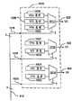
図6は、本発明にもとづく多重ピクセルディスプレイのブロック図を示す。
【図7】
図7は、図6のディスプレイの単一ピクセルセルを詳細に示す。
【図8】
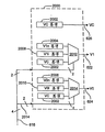
図8は、図7の電圧コントローラの1つの実施形態のブロック図である。
【図9】
図9は、図6のディスプレイの1つの実施形態に、多数の2値重みつきデータビットを書き込むためのタイミング図を示す。
【図10】
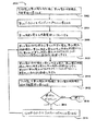
図10は、図9のタイミング図を実行するための方法を要約したフローチャートである。
【図11】
図11は、グレースケール値をRMS電圧の有効な範囲に限定するために、本発明にもとづいて修正されたRMS電圧対グレースケール値曲線である。
【図12A】
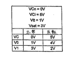
図12Aは、本発明の1つの実施形態に用いられる変調方式およびデバイアシング方式を示す電圧方式である。
【図12B】
図12Bは、図12Aに示される電圧のサンプル値を示す表である。
【図13】
図13は、本発明にもとづいて特定の駆動方式を実行するための別の電圧コントローラのブロック図である。
【図14】
図14は、図12Aの電圧方式の実行を示すタイミング図である。
【図15】
図15は、図13の駆動方式の方法を要約したフローチャートである。
【図16】
図16は、本発明にもとづいて特定の駆動方式を実行するための別の電圧コントローラのブロック図である。
【図17】
図17は、図12Aの電圧方式の実行を示すタイミング図である。
【図18】
図18は、図17の駆動方式にもとづいて図6のディスプレイを駆動するための方法を要約したフローチャートである。
【図19A】
図19Aは、本発明の1つの実施形態に用いられる変調方式およびデバイアス方式を示す電圧方式である。
【図19B】
図19Bは、図19Aに示される電圧のサンプル値を示す表である。
【図20】
図20は、本発明にもとづいて特定の駆動方式を実行するための別の電圧コントローラのブロック図である。
【図21A】
図21Aは、図19Aの電圧方式の実行を示すタイミング図である。
【図21B】
図21Bは、図19Aの電圧方式の別の実行を示すタイミング図ある。
【図22】
図22は、図21Aおよび21Bの駆動方式にもとづいて、図6のディスプレイを駆動するための方法を要約したフローチャートである。
【図23A】
図23Aは、本発明の1つの実施形態に用いられる変調方式およびデバイアシング方式を示す図である。
【図23B】
図23Bは、図23Aに示されるサンプル値を示す表である。
【図24】
図24は、本発明にもとづいて、特定の駆動方式を実行するための別の電圧コントローラのブロック図である。
【図25】
図25は、図23Aの電圧方式の実行を示すタイミング図である。
【図26】
図26は、図25の駆動方式にもとづいて、図6のディスプレイを駆動するための方法を要約したフローチャートである。
【図27】
図27は、本発明にもとづいて、特定の駆動方式を実行するための別の電圧コントローラのブロック図である。
【図28】
図28は、図6のディスプレイを用いて別の駆動方式を示すタイミング図である。
【図29】
図29は、図28の駆動方式にもとづいて、図6のディスプレイを駆動するための方法を要約したフローチャートである。
【図30】
図30は、図6のディスプレイを用いて別の駆動方式を示すタイミング図である。
【図31】
図31は、図30の駆動方式にもとづいて、図6のディスプレイを駆動するための方法を要約したフローチャートである。
【図32】
図32は、本発明にもとづいて、特定の駆動方式を実行するための別の電圧コントローラのブロック図である。
【図33】
図33は、本発明にもとづいて、別の駆動方式を示すタイミング図である。
【図34】
図34は、本発明にもとづいて、特定の駆動方式を実行することが可能な別の電圧コントローラのブロック図である。
【図35】
図35は、本発明にもとづいて、別の駆動方式を示すタイミング図である。
【図36】
図36は、単一の制御信号により動作可能な別の電圧コントローラである。
Claims (2)
- 複数のピクセル電極、複数の記憶素子、第1の電圧供給端子、第2の電圧供給端子、共通電極、および複数のマルチプレクサを備えるディスプレイ上にマルチビットデータワードを表示する方法であって、該複数のマルチプレクサの各々は、該記憶素子のうちの関連付けられた1つに記憶されたデータビットの値に応答して、該ピクセル電極のうちの関連付けられた1つを該第1の電圧供給端子および該第2の電圧供給端子のうちの1方と選択的に接続し、ここで該方法は、第1の所定の電圧を該第1の電圧供給端子に、第2の所定の電圧を該第2の電圧供給端子に、そして第3の所定の電圧を該共通電極に有効な状態とする工程と、該マルチビットデータワードの各ビットを該記憶素子に連続的に書き込む工程と、該ビットの各々を、該ビットの各々の位に依存する期間の間、該記憶素子中に残留させる工程と、を包含し、
前記第1の所定の電圧と前記第2の所定の電圧が前記ディスプレイの論理レベルから独立し、前記ディスプレイが液晶ディスプレイであり、前記第1の所定の電圧と前記第3の所定の電圧との差が液晶セルの飽和電圧に対応し、前記第2の所定の電圧と前記第3の所定の電圧との差が当該液晶セルの閾値電圧に対応し、第4の所定の電圧を前記共通電極に有効な状態とする工程と、前記記憶素子に書き込まれた前記マルチビットデータワードの各ビットの相補ビットを前記記憶素子に書き込む工程と、該マルチビットデータワードの各ビットの該相補ビットを該ビットの各々の位に依存する期間の間、該記憶素子中に残留させる工程と、をさらに包含する
ことを特徴とする方法。
- ディスプレイ駆動回路に請求項1に記載の工程を行わせるためのプログラムを備えるコンピュータに実行させるためのプログラムを記録したコンピュータ読み取り可能な記録媒体。
Applications Claiming Priority (3)
| Application Number | Priority Date | Filing Date | Title |
|---|---|---|---|
| US09/075,472 US6067065A (en) | 1998-05-08 | 1998-05-08 | Method for modulating a multiplexed pixel display |
| US09/075,472 | 1998-05-08 | ||
| PCT/US1999/010115 WO1999059127A1 (en) | 1998-05-08 | 1999-05-07 | Method for modulating a multiplexed pixel display |
Related Child Applications (1)
| Application Number | Title | Priority Date | Filing Date |
|---|---|---|---|
| JP2011278841A Division JP2012098745A (ja) | 1998-05-08 | 2011-12-20 | 飽和電圧と閾値電圧間の変調を達成するための多重ピクセルを備えたディスプレイ |
Publications (3)
| Publication Number | Publication Date |
|---|---|
| JP2002514796A JP2002514796A (ja) | 2002-05-21 |
| JP2002514796A5 JP2002514796A5 (ja) | 2010-09-24 |
| JP5327824B2 true JP5327824B2 (ja) | 2013-10-30 |
Family
ID=22125985
Family Applications (2)
| Application Number | Title | Priority Date | Filing Date |
|---|---|---|---|
| JP2000548859A Expired - Lifetime JP5327824B2 (ja) | 1998-05-08 | 1999-05-07 | 飽和電圧と閾値電圧間の変調を達成するための多重ピクセルを備えたディスプレイ |
| JP2011278841A Pending JP2012098745A (ja) | 1998-05-08 | 2011-12-20 | 飽和電圧と閾値電圧間の変調を達成するための多重ピクセルを備えたディスプレイ |
Family Applications After (1)
| Application Number | Title | Priority Date | Filing Date |
|---|---|---|---|
| JP2011278841A Pending JP2012098745A (ja) | 1998-05-08 | 2011-12-20 | 飽和電圧と閾値電圧間の変調を達成するための多重ピクセルを備えたディスプレイ |
Country Status (8)
| Country | Link |
|---|---|
| US (4) | US6067065A (ja) |
| EP (1) | EP1093654B1 (ja) |
| JP (2) | JP5327824B2 (ja) |
| CN (1) | CN1174358C (ja) |
| AT (1) | ATE450029T1 (ja) |
| CA (1) | CA2331695C (ja) |
| DE (1) | DE69941706D1 (ja) |
| WO (1) | WO1999059127A1 (ja) |
Families Citing this family (38)
| Publication number | Priority date | Publication date | Assignee | Title |
|---|---|---|---|---|
| US6067065A (en) * | 1998-05-08 | 2000-05-23 | Aurora Systems, Inc. | Method for modulating a multiplexed pixel display |
| JP3914639B2 (ja) * | 1998-07-13 | 2007-05-16 | 株式会社アドバンスト・ディスプレイ | 液晶表示装置 |
| US6278428B1 (en) * | 1999-03-24 | 2001-08-21 | Intel Corporation | Display panel |
| US7872871B2 (en) | 2000-01-06 | 2011-01-18 | Super Talent Electronics, Inc. | Molding methods to manufacture single-chip chip-on-board USB device |
| US7257714B1 (en) * | 1999-10-19 | 2007-08-14 | Super Talent Electronics, Inc. | Electronic data storage medium with fingerprint verification capability |
| US8625270B2 (en) | 1999-08-04 | 2014-01-07 | Super Talent Technology, Corp. | USB flash drive with deploying and retracting functionalities using retractable cover/cap |
| US7466556B2 (en) * | 1999-08-04 | 2008-12-16 | Super Talent Electronics, Inc. | Single chip USB packages with swivel cover |
| US8102662B2 (en) | 2007-07-05 | 2012-01-24 | Super Talent Electronics, Inc. | USB package with bistable sliding mechanism |
| US6507330B1 (en) * | 1999-09-01 | 2003-01-14 | Displaytech, Inc. | DC-balanced and non-DC-balanced drive schemes for liquid crystal devices |
| TW494382B (en) * | 2000-03-22 | 2002-07-11 | Toshiba Corp | Display apparatus and driving method of display apparatus |
| KR100585962B1 (ko) * | 2000-12-20 | 2006-06-07 | 일진다이아몬드 주식회사 서울지사 | 디지털 광밸브 어드레싱 방법 및 장치와 이것을 포함하는광밸브 |
| US7071908B2 (en) | 2003-05-20 | 2006-07-04 | Kagutech, Ltd. | Digital backplane |
| US8998620B2 (en) * | 2003-12-02 | 2015-04-07 | Super Talent Technology, Corp. | Molding method for COB-EUSB devices and metal housing package |
| US8102657B2 (en) | 2003-12-02 | 2012-01-24 | Super Talent Electronics, Inc. | Single shot molding method for COB USB/EUSB devices with contact pad ribs |
| US7050027B1 (en) | 2004-01-16 | 2006-05-23 | Maxim Integrated Products, Inc. | Single wire interface for LCD calibrator |
| US7815469B1 (en) | 2004-02-12 | 2010-10-19 | Super Talent Electronics, Inc. | Dual-personality extended USB plugs and receptacles using with PCBA and cable assembly |
| US8885139B2 (en) | 2005-01-21 | 2014-11-11 | Johnson & Johnson Vision Care | Adaptive electro-active lens with variable focal length |
| US7557789B2 (en) * | 2005-05-09 | 2009-07-07 | Texas Instruments Incorporated | Data-dependent, logic-level drive scheme for driving LCD panels |
| US7541693B2 (en) * | 2005-06-13 | 2009-06-02 | Intel Corporation | Power distribution network for computer systems and other low-power applications |
| CN101501616B (zh) * | 2006-06-12 | 2012-02-22 | 庄臣及庄臣视力保护公司 | 利用电-光透镜降低功耗的方法 |
| US20080212007A1 (en) * | 2006-09-01 | 2008-09-04 | Gerald Meredith | Electro-Optic Lenses Employing Resistive Electrodes |
| US8102658B2 (en) | 2007-07-05 | 2012-01-24 | Super Talent Electronics, Inc. | Micro-SD to secure digital adaptor card and manufacturing method |
| CN101981495B (zh) * | 2008-03-28 | 2012-11-28 | 富士通株式会社 | 胆甾型液晶面板的多灰度驱动电路、驱动方法及显示装置 |
| EP2579243A4 (en) * | 2010-06-01 | 2013-11-13 | Sharp Kk | DISPLAY DEVICE |
| JP5831325B2 (ja) * | 2012-03-28 | 2015-12-09 | 株式会社Jvcケンウッド | 液晶表示装置及びその駆動方法 |
| US9406269B2 (en) | 2013-03-15 | 2016-08-02 | Jasper Display Corp. | System and method for pulse width modulating a scrolling color display |
| US20140368561A1 (en) * | 2013-06-17 | 2014-12-18 | Jasper Display Corp. | Method For Modulating A Micro-Led Display |
| CN103606362A (zh) * | 2013-11-27 | 2014-02-26 | 深圳市长江力伟股份有限公司 | 液晶显示器的数字脉宽调制灰度的方法及液晶显示器 |
| US9918053B2 (en) | 2014-05-14 | 2018-03-13 | Jasper Display Corp. | System and method for pulse-width modulating a phase-only spatial light modulator |
| CA2873476A1 (en) * | 2014-12-08 | 2016-06-08 | Ignis Innovation Inc. | Smart-pixel display architecture |
| US11030942B2 (en) | 2017-10-13 | 2021-06-08 | Jasper Display Corporation | Backplane adaptable to drive emissive pixel arrays of differing pitches |
| US10951875B2 (en) | 2018-07-03 | 2021-03-16 | Raxium, Inc. | Display processing circuitry |
| US11710445B2 (en) | 2019-01-24 | 2023-07-25 | Google Llc | Backplane configurations and operations |
| US11637219B2 (en) | 2019-04-12 | 2023-04-25 | Google Llc | Monolithic integration of different light emitting structures on a same substrate |
| US11238782B2 (en) | 2019-06-28 | 2022-02-01 | Jasper Display Corp. | Backplane for an array of emissive elements |
| US11626062B2 (en) | 2020-02-18 | 2023-04-11 | Google Llc | System and method for modulating an array of emissive elements |
| US11538431B2 (en) | 2020-06-29 | 2022-12-27 | Google Llc | Larger backplane suitable for high speed applications |
| WO2023287936A1 (en) | 2021-07-14 | 2023-01-19 | Google Llc | Backplane and method for pulse width modulation |
Family Cites Families (28)
| Publication number | Priority date | Publication date | Assignee | Title |
|---|---|---|---|---|
| JPS54100224A (en) * | 1978-01-25 | 1979-08-07 | Hitachi Ltd | Luminance modulator for liquid crystal display unit |
| JPS5653487A (en) * | 1979-10-05 | 1981-05-13 | Seiko Epson Corp | Liquid-crystal indication device for clock |
| JPS5823091A (ja) | 1981-08-04 | 1983-02-10 | セイコーインスツルメンツ株式会社 | 画像表示装置 |
| NL8503180A (nl) * | 1985-11-19 | 1987-06-16 | Philips Nv | Weergeefinrichting. |
| JPH02135419A (ja) * | 1988-11-17 | 1990-05-24 | Seiko Epson Corp | 液晶表示装置の駆動法 |
| JPH03132692A (ja) * | 1989-10-18 | 1991-06-06 | Matsushita Electric Ind Co Ltd | 液晶表示装置の駆動方法及びその駆動回路 |
| JP2941987B2 (ja) * | 1990-04-09 | 1999-08-30 | キヤノン株式会社 | 液晶表示装置およびその駆動方法 |
| JPH04149517A (ja) | 1990-10-12 | 1992-05-22 | Nec Corp | 液晶駆動回路 |
| JPH04260092A (ja) * | 1991-02-15 | 1992-09-16 | Oki Electric Ind Co Ltd | 液晶表示装置の映像信号処理回路 |
| JP3482667B2 (ja) * | 1993-01-13 | 2003-12-22 | セイコーエプソン株式会社 | 液晶表示装置の駆動方法及び液晶表示装置 |
| US5459495A (en) * | 1992-05-14 | 1995-10-17 | In Focus Systems, Inc. | Gray level addressing for LCDs |
| US5731796A (en) * | 1992-10-15 | 1998-03-24 | Hitachi, Ltd. | Liquid crystal display driving method/driving circuit capable of being driven with equal voltages |
| US5471225A (en) * | 1993-04-28 | 1995-11-28 | Dell Usa, L.P. | Liquid crystal display with integrated frame buffer |
| US5673061A (en) * | 1993-05-14 | 1997-09-30 | Sharp Kabushiki Kaisha | Driving circuit for display apparatus |
| JP2604750Y2 (ja) | 1993-12-29 | 2000-06-05 | カシオ計算機株式会社 | 表示駆動装置 |
| JPH08101367A (ja) * | 1994-08-05 | 1996-04-16 | Sanyo Electric Co Ltd | 立体画像表示装置 |
| JP3790277B2 (ja) * | 1994-11-24 | 2006-06-28 | テキサス インスツルメンツ インコーポレイテツド | パルス幅変調ディジタル表示画素の強度調節方法及びこの方法を適用される表示システム |
| JP3630489B2 (ja) * | 1995-02-16 | 2005-03-16 | 株式会社東芝 | 液晶表示装置 |
| US5959598A (en) * | 1995-07-20 | 1999-09-28 | The Regents Of The University Of Colorado | Pixel buffer circuits for implementing improved methods of displaying grey-scale or color images |
| US5945972A (en) * | 1995-11-30 | 1999-08-31 | Kabushiki Kaisha Toshiba | Display device |
| KR100270147B1 (ko) * | 1996-03-01 | 2000-10-16 | 니시무로 타이죠 | 액정표시장치 |
| JP3305946B2 (ja) * | 1996-03-07 | 2002-07-24 | 株式会社東芝 | 液晶表示装置 |
| EP0797182A1 (en) * | 1996-03-19 | 1997-09-24 | Hitachi, Ltd. | Active matrix LCD with data holding circuit in each pixel |
| US5952991A (en) * | 1996-11-14 | 1999-09-14 | Kabushiki Kaisha Toshiba | Liquid crystal display |
| US5977942A (en) * | 1996-12-20 | 1999-11-02 | Compaq Computer Corporation | Multiplexed display element sequential color LCD panel |
| US6518945B1 (en) * | 1997-07-25 | 2003-02-11 | Aurora Systems, Inc. | Replacing defective circuit elements by column and row shifting in a flat-panel display |
| US6067065A (en) * | 1998-05-08 | 2000-05-23 | Aurora Systems, Inc. | Method for modulating a multiplexed pixel display |
| US6005558A (en) * | 1998-05-08 | 1999-12-21 | Aurora Systems, Inc. | Display with multiplexed pixels for achieving modulation between saturation and threshold voltages |
-
1998
- 1998-05-08 US US09/075,472 patent/US6067065A/en not_active Expired - Lifetime
-
1999
- 1999-05-07 DE DE69941706T patent/DE69941706D1/de not_active Expired - Lifetime
- 1999-05-07 CA CA002331695A patent/CA2331695C/en not_active Expired - Lifetime
- 1999-05-07 JP JP2000548859A patent/JP5327824B2/ja not_active Expired - Lifetime
- 1999-05-07 AT AT99920403T patent/ATE450029T1/de not_active IP Right Cessation
- 1999-05-07 WO PCT/US1999/010115 patent/WO1999059127A1/en active Application Filing
- 1999-05-07 CN CNB998082465A patent/CN1174358C/zh not_active Expired - Lifetime
- 1999-05-07 EP EP99920403A patent/EP1093654B1/en not_active Expired - Lifetime
-
2000
- 2000-03-27 US US09/536,858 patent/US6980188B1/en not_active Expired - Lifetime
-
2005
- 2005-09-20 US US11/231,123 patent/US7379043B2/en not_active Expired - Lifetime
-
2008
- 2008-05-23 US US12/154,602 patent/US8344980B2/en not_active Expired - Fee Related
-
2011
- 2011-12-20 JP JP2011278841A patent/JP2012098745A/ja active Pending
Also Published As
| Publication number | Publication date |
|---|---|
| US6980188B1 (en) | 2005-12-27 |
| EP1093654A1 (en) | 2001-04-25 |
| US20060012594A1 (en) | 2006-01-19 |
| US7379043B2 (en) | 2008-05-27 |
| US6067065A (en) | 2000-05-23 |
| EP1093654B1 (en) | 2009-11-25 |
| JP2012098745A (ja) | 2012-05-24 |
| CA2331695A1 (en) | 1999-11-18 |
| CN1308756A (zh) | 2001-08-15 |
| EP1093654A4 (en) | 2007-10-31 |
| ATE450029T1 (de) | 2009-12-15 |
| CA2331695C (en) | 2008-03-04 |
| US8344980B2 (en) | 2013-01-01 |
| DE69941706D1 (de) | 2010-01-07 |
| WO1999059127A1 (en) | 1999-11-18 |
| CN1174358C (zh) | 2004-11-03 |
| US20080225030A1 (en) | 2008-09-18 |
| JP2002514796A (ja) | 2002-05-21 |
Similar Documents
| Publication | Publication Date | Title |
|---|---|---|
| JP5327824B2 (ja) | 飽和電圧と閾値電圧間の変調を達成するための多重ピクセルを備えたディスプレイ | |
| EP1082718B1 (en) | Display with multiplexed pixels for achieving modulation between saturation and threshold voltages | |
| US5670973A (en) | Method and apparatus for compensating crosstalk in liquid crystal displays | |
| US6762739B2 (en) | System and method for reducing the intensity output rise time in a liquid crystal display | |
| US6801177B2 (en) | Liquid crystal display device | |
| JP3568615B2 (ja) | 液晶駆動装置,その制御方法及び液晶表示装置 | |
| JP3704984B2 (ja) | 液晶表示装置 | |
| JP2988815B2 (ja) | 液晶駆動装置 | |
| US8743041B2 (en) | Liquid crystal display drive circuit and liquid crystal display device | |
| US6630919B1 (en) | Optical modulator and integrated circuit therefor | |
| KR100453186B1 (ko) | 강유전성액정표시장치및그구동방법 | |
| JP2002229520A (ja) | 平面表示装置およびその駆動方法 | |
| JPH04358197A (ja) | 液晶ディスプレイの階調駆動回路 | |
| JPH0469392B2 (ja) | ||
| GB2428509A (en) | Driver circuit for a display element | |
| JP2007102158A (ja) | 液晶画像表示装置の及びその駆動方法 | |
| JPH04241382A (ja) | フラットディスプレイの階調駆動回路 |
Legal Events
| Date | Code | Title | Description |
|---|---|---|---|
| A621 | Written request for application examination |
Free format text: JAPANESE INTERMEDIATE CODE: A621 Effective date: 20060412 |
|
| RD02 | Notification of acceptance of power of attorney |
Free format text: JAPANESE INTERMEDIATE CODE: A7422 Effective date: 20091210 |
|
| A131 | Notification of reasons for refusal |
Free format text: JAPANESE INTERMEDIATE CODE: A131 Effective date: 20100201 |
|
| A601 | Written request for extension of time |
Free format text: JAPANESE INTERMEDIATE CODE: A601 Effective date: 20100423 |
|
| A602 | Written permission of extension of time |
Free format text: JAPANESE INTERMEDIATE CODE: A602 Effective date: 20100506 |
|
| A601 | Written request for extension of time |
Free format text: JAPANESE INTERMEDIATE CODE: A601 Effective date: 20100528 |
|
| A602 | Written permission of extension of time |
Free format text: JAPANESE INTERMEDIATE CODE: A602 Effective date: 20100604 |
|
| A601 | Written request for extension of time |
Free format text: JAPANESE INTERMEDIATE CODE: A601 Effective date: 20100630 |
|
| A602 | Written permission of extension of time |
Free format text: JAPANESE INTERMEDIATE CODE: A602 Effective date: 20100707 |
|
| A524 | Written submission of copy of amendment under article 19 pct |
Free format text: JAPANESE INTERMEDIATE CODE: A524 Effective date: 20100802 |
|
| RD04 | Notification of resignation of power of attorney |
Free format text: JAPANESE INTERMEDIATE CODE: A7424 Effective date: 20110126 |
|
| A02 | Decision of refusal |
Free format text: JAPANESE INTERMEDIATE CODE: A02 Effective date: 20110829 |
|
| A521 | Request for written amendment filed |
Free format text: JAPANESE INTERMEDIATE CODE: A523 Effective date: 20111220 |
|
| A911 | Transfer to examiner for re-examination before appeal (zenchi) |
Free format text: JAPANESE INTERMEDIATE CODE: A911 Effective date: 20120209 |
|
| A711 | Notification of change in applicant |
Free format text: JAPANESE INTERMEDIATE CODE: A711 Effective date: 20120829 |
|
| A521 | Request for written amendment filed |
Free format text: JAPANESE INTERMEDIATE CODE: A821 Effective date: 20120829 |
|
| A912 | Re-examination (zenchi) completed and case transferred to appeal board |
Free format text: JAPANESE INTERMEDIATE CODE: A912 Effective date: 20121005 |
|
| A521 | Request for written amendment filed |
Free format text: JAPANESE INTERMEDIATE CODE: A523 Effective date: 20130524 |
|
| A61 | First payment of annual fees (during grant procedure) |
Free format text: JAPANESE INTERMEDIATE CODE: A61 Effective date: 20130718 |
|
| R150 | Certificate of patent or registration of utility model |
Free format text: JAPANESE INTERMEDIATE CODE: R150 |
|
| R250 | Receipt of annual fees |
Free format text: JAPANESE INTERMEDIATE CODE: R250 |
|
| R250 | Receipt of annual fees |
Free format text: JAPANESE INTERMEDIATE CODE: R250 |
|
| R250 | Receipt of annual fees |
Free format text: JAPANESE INTERMEDIATE CODE: R250 |
|
| EXPY | Cancellation because of completion of term |