JP5323501B2 - Light emitting diode package and manufacturing method thereof - Google Patents
Light emitting diode package and manufacturing method thereof Download PDFInfo
- Publication number
- JP5323501B2 JP5323501B2 JP2008557208A JP2008557208A JP5323501B2 JP 5323501 B2 JP5323501 B2 JP 5323501B2 JP 2008557208 A JP2008557208 A JP 2008557208A JP 2008557208 A JP2008557208 A JP 2008557208A JP 5323501 B2 JP5323501 B2 JP 5323501B2
- Authority
- JP
- Japan
- Prior art keywords
- light emitting
- emitting diode
- metal plate
- insulating layer
- diode package
- Prior art date
- Legal status (The legal status is an assumption and is not a legal conclusion. Google has not performed a legal analysis and makes no representation as to the accuracy of the status listed.)
- Active
Links
- 238000004519 manufacturing process Methods 0.000 title claims description 16
- 229910052751 metal Inorganic materials 0.000 claims description 44
- 239000002184 metal Substances 0.000 claims description 44
- 238000000034 method Methods 0.000 claims description 24
- 239000011347 resin Substances 0.000 claims description 18
- 229920005989 resin Polymers 0.000 claims description 18
- VTYYLEPIZMXCLO-UHFFFAOYSA-L Calcium carbonate Chemical compound [Ca+2].[O-]C([O-])=O VTYYLEPIZMXCLO-UHFFFAOYSA-L 0.000 claims description 6
- XLOMVQKBTHCTTD-UHFFFAOYSA-N Zinc monoxide Chemical compound [Zn]=O XLOMVQKBTHCTTD-UHFFFAOYSA-N 0.000 claims description 6
- TZCXTZWJZNENPQ-UHFFFAOYSA-L barium sulfate Chemical compound [Ba+2].[O-]S([O-])(=O)=O TZCXTZWJZNENPQ-UHFFFAOYSA-L 0.000 claims description 6
- 238000007650 screen-printing Methods 0.000 claims description 4
- 229910000019 calcium carbonate Inorganic materials 0.000 claims description 3
- 239000011787 zinc oxide Substances 0.000 claims description 3
- GWEVSGVZZGPLCZ-UHFFFAOYSA-N Titan oxide Chemical compound O=[Ti]=O GWEVSGVZZGPLCZ-UHFFFAOYSA-N 0.000 claims description 2
- 238000000465 moulding Methods 0.000 claims description 2
- 239000000126 substance Substances 0.000 claims description 2
- OGIDPMRJRNCKJF-UHFFFAOYSA-N titanium oxide Inorganic materials [Ti]=O OGIDPMRJRNCKJF-UHFFFAOYSA-N 0.000 claims description 2
- 230000017525 heat dissipation Effects 0.000 description 6
- 230000000694 effects Effects 0.000 description 4
- 239000007788 liquid Substances 0.000 description 3
- 238000005530 etching Methods 0.000 description 2
- 238000007731 hot pressing Methods 0.000 description 2
- 239000007769 metal material Substances 0.000 description 2
- RYGMFSIKBFXOCR-UHFFFAOYSA-N Copper Chemical compound [Cu] RYGMFSIKBFXOCR-UHFFFAOYSA-N 0.000 description 1
- 239000004593 Epoxy Substances 0.000 description 1
- XUIMIQQOPSSXEZ-UHFFFAOYSA-N Silicon Chemical compound [Si] XUIMIQQOPSSXEZ-UHFFFAOYSA-N 0.000 description 1
- 238000000137 annealing Methods 0.000 description 1
- 238000000576 coating method Methods 0.000 description 1
- 229910052802 copper Inorganic materials 0.000 description 1
- 239000010949 copper Substances 0.000 description 1
- 238000005553 drilling Methods 0.000 description 1
- 239000011521 glass Substances 0.000 description 1
- 229910052737 gold Inorganic materials 0.000 description 1
- 239000000463 material Substances 0.000 description 1
- 238000010297 mechanical methods and process Methods 0.000 description 1
- 238000001465 metallisation Methods 0.000 description 1
- 238000003801 milling Methods 0.000 description 1
- 230000003287 optical effect Effects 0.000 description 1
- 238000000206 photolithography Methods 0.000 description 1
- 239000004065 semiconductor Substances 0.000 description 1
- 229910052710 silicon Inorganic materials 0.000 description 1
- 239000010703 silicon Substances 0.000 description 1
- 239000012463 white pigment Substances 0.000 description 1
Images


Classifications
-
- F—MECHANICAL ENGINEERING; LIGHTING; HEATING; WEAPONS; BLASTING
- F24—HEATING; RANGES; VENTILATING
- F24C—DOMESTIC STOVES OR RANGES ; DETAILS OF DOMESTIC STOVES OR RANGES, OF GENERAL APPLICATION
- F24C7/00—Stoves or ranges heated by electric energy
- F24C7/06—Arrangement or mounting of electric heating elements
- F24C7/062—Arrangement or mounting of electric heating elements on stoves
- F24C7/065—Arrangement or mounting of electric heating elements on stoves with reflectors
-
- H—ELECTRICITY
- H01—ELECTRIC ELEMENTS
- H01L—SEMICONDUCTOR DEVICES NOT COVERED BY CLASS H10
- H01L33/00—Semiconductor devices having potential barriers specially adapted for light emission; Processes or apparatus specially adapted for the manufacture or treatment thereof or of parts thereof; Details thereof
- H01L33/48—Semiconductor devices having potential barriers specially adapted for light emission; Processes or apparatus specially adapted for the manufacture or treatment thereof or of parts thereof; Details thereof characterised by the semiconductor body packages
- H01L33/64—Heat extraction or cooling elements
- H01L33/642—Heat extraction or cooling elements characterized by the shape
-
- F—MECHANICAL ENGINEERING; LIGHTING; HEATING; WEAPONS; BLASTING
- F24—HEATING; RANGES; VENTILATING
- F24C—DOMESTIC STOVES OR RANGES ; DETAILS OF DOMESTIC STOVES OR RANGES, OF GENERAL APPLICATION
- F24C7/00—Stoves or ranges heated by electric energy
- F24C7/08—Arrangement or mounting of control or safety devices
- F24C7/081—Arrangement or mounting of control or safety devices on stoves
-
- H—ELECTRICITY
- H01—ELECTRIC ELEMENTS
- H01L—SEMICONDUCTOR DEVICES NOT COVERED BY CLASS H10
- H01L33/00—Semiconductor devices having potential barriers specially adapted for light emission; Processes or apparatus specially adapted for the manufacture or treatment thereof or of parts thereof; Details thereof
- H01L33/48—Semiconductor devices having potential barriers specially adapted for light emission; Processes or apparatus specially adapted for the manufacture or treatment thereof or of parts thereof; Details thereof characterised by the semiconductor body packages
- H01L33/483—Containers
- H01L33/486—Containers adapted for surface mounting
-
- H—ELECTRICITY
- H01—ELECTRIC ELEMENTS
- H01L—SEMICONDUCTOR DEVICES NOT COVERED BY CLASS H10
- H01L2224/00—Indexing scheme for arrangements for connecting or disconnecting semiconductor or solid-state bodies and methods related thereto as covered by H01L24/00
- H01L2224/01—Means for bonding being attached to, or being formed on, the surface to be connected, e.g. chip-to-package, die-attach, "first-level" interconnects; Manufacturing methods related thereto
- H01L2224/42—Wire connectors; Manufacturing methods related thereto
- H01L2224/47—Structure, shape, material or disposition of the wire connectors after the connecting process
- H01L2224/48—Structure, shape, material or disposition of the wire connectors after the connecting process of an individual wire connector
- H01L2224/4805—Shape
- H01L2224/4809—Loop shape
- H01L2224/48091—Arched
-
- H—ELECTRICITY
- H01—ELECTRIC ELEMENTS
- H01L—SEMICONDUCTOR DEVICES NOT COVERED BY CLASS H10
- H01L2924/00—Indexing scheme for arrangements or methods for connecting or disconnecting semiconductor or solid-state bodies as covered by H01L24/00
- H01L2924/0001—Technical content checked by a classifier
- H01L2924/00014—Technical content checked by a classifier the subject-matter covered by the group, the symbol of which is combined with the symbol of this group, being disclosed without further technical details
-
- H—ELECTRICITY
- H01—ELECTRIC ELEMENTS
- H01L—SEMICONDUCTOR DEVICES NOT COVERED BY CLASS H10
- H01L33/00—Semiconductor devices having potential barriers specially adapted for light emission; Processes or apparatus specially adapted for the manufacture or treatment thereof or of parts thereof; Details thereof
- H01L33/48—Semiconductor devices having potential barriers specially adapted for light emission; Processes or apparatus specially adapted for the manufacture or treatment thereof or of parts thereof; Details thereof characterised by the semiconductor body packages
- H01L33/58—Optical field-shaping elements
- H01L33/60—Reflective elements
-
- H—ELECTRICITY
- H01—ELECTRIC ELEMENTS
- H01L—SEMICONDUCTOR DEVICES NOT COVERED BY CLASS H10
- H01L33/00—Semiconductor devices having potential barriers specially adapted for light emission; Processes or apparatus specially adapted for the manufacture or treatment thereof or of parts thereof; Details thereof
- H01L33/48—Semiconductor devices having potential barriers specially adapted for light emission; Processes or apparatus specially adapted for the manufacture or treatment thereof or of parts thereof; Details thereof characterised by the semiconductor body packages
- H01L33/64—Heat extraction or cooling elements
- H01L33/644—Heat extraction or cooling elements in intimate contact or integrated with parts of the device other than the semiconductor body
Landscapes
- Engineering & Computer Science (AREA)
- Microelectronics & Electronic Packaging (AREA)
- Manufacturing & Machinery (AREA)
- Computer Hardware Design (AREA)
- Power Engineering (AREA)
- Chemical & Material Sciences (AREA)
- Combustion & Propulsion (AREA)
- Mechanical Engineering (AREA)
- General Engineering & Computer Science (AREA)
- Led Device Packages (AREA)
- Devices For Indicating Variable Information By Combining Individual Elements (AREA)
Description
本発明は、発光ダイオードパッケージ及び発光ダイオードパッケージの製造方法に関するものである。 The present invention relates to a light emitting diode package and a method for manufacturing the light emitting diode package.
発光ダイオードパッケージは、発光ダイオードと、上記発光ダイオードに駆動信号を印加し、上記発光ダイオードを支持する印刷回路基板が含まれて構成される。 The light emitting diode package includes a light emitting diode and a printed circuit board that applies a driving signal to the light emitting diode and supports the light emitting diode.
上記発光ダイオードは、電気エネルギーを光に変換する素子であって、電気エネルギーが光に変換される過程で熱が発生され、発生された熱により発光ダイオードの駆動特性が劣化する問題がある。 The light emitting diode is an element that converts electric energy into light, and heat is generated in the process of converting the electric energy into light, and there is a problem that driving characteristics of the light emitting diode deteriorate due to the generated heat.
したがって、発光ダイオードから発生された熱を効果的に放出されるようにする必要がある。 Therefore, it is necessary to effectively release the heat generated from the light emitting diode.
一方、発光ダイオードパッケージでは、発光ダイオードから発生された熱が迅速に放出できるように印刷回路基板に放熱部材を取り付ける場合がある。 On the other hand, in a light emitting diode package, a heat dissipation member may be attached to a printed circuit board so that heat generated from the light emitting diode can be quickly released.
しかしながら、放熱部材を取り付ける場合、工程が複雑になり、費用が増加する短所がある。 However, when the heat dissipating member is attached, the process becomes complicated and the cost increases.
また、放熱部材の取付位置によって発光ダイオードから放出された光を遮断して発光ダイオードチップの発光効率を低下させる。 Further, the light emitted from the light emitting diode is blocked by the mounting position of the heat dissipating member to reduce the light emitting efficiency of the light emitting diode chip.
本発明の目的は、発光ダイオードチップから発生された熱を効果的に放出できるようにする発光ダイオードパッケージ及び発光ダイオードパッケージの製造方法を提供することにある。 An object of the present invention is to provide a light emitting diode package and a method for manufacturing the light emitting diode package that can effectively release heat generated from the light emitting diode chip.
本発明の他の目的は、発光ダイオードチップから発生された熱を効果的に放出できるようにしながら、発光効率の低下を防止できる発光ダイオードパッケージ及び発光ダイオードパッケージの製造方法を提供することにある。 It is another object of the present invention to provide a light emitting diode package and a method for manufacturing the light emitting diode package that can prevent a decrease in light emission efficiency while effectively releasing heat generated from the light emitting diode chip.
本発明による発光ダイオードパッケージは、溝が形成された金属板、上記金属板の上の絶縁層、上記絶縁層の上の回路パターン、及び上記回路パターンと電気的に連結された上記絶縁層の上の発光ダイオードが含まれる。 The light emitting diode package according to the present invention includes a metal plate having a groove, an insulating layer on the metal plate, a circuit pattern on the insulating layer, and an insulating layer electrically connected to the circuit pattern. Of light emitting diodes.
また、本発明による発光ダイオードパッケージの製造方法は、MCPCB(Metal Core Printed Circuit Board)を準備する段階と、上記MCPCBに含まれた金属板を選択的に除去して溝を形成する段階と、上記MCPCBの上に発光ダイオードを実装する段階が含まれる。 The method for manufacturing a light emitting diode package according to the present invention includes a step of preparing an MCPCB (Metal Core Printed Circuit Board), a step of selectively removing a metal plate included in the MCPCB and forming a groove, The step of mounting the light emitting diode on the MCPCB is included.
また、本発明による装置は、溝が形成された金属板と、上記金属板の上の絶縁層と、上記絶縁層の上の回路パターンと、上記回路パターンと電気的に連結された前記絶縁層の上の電子素子が含まれる。 The apparatus according to the present invention also includes a metal plate having grooves, an insulating layer on the metal plate, a circuit pattern on the insulating layer, and the insulating layer electrically connected to the circuit pattern. An electronic device above is included.
本発明による発光ダイオードパッケージは、熱を効果的に放出することができる。 The light emitting diode package according to the present invention can effectively release heat.
本発明による発光ダイオードパッケージは、発光ダイオードチップの発光効率を低下させないで、効果的に熱を放出することができる。 The light emitting diode package according to the present invention can effectively dissipate heat without reducing the light emission efficiency of the light emitting diode chip.
以下、添付図面を参照しつつ本発明の実施形態を詳細に説明する。 Hereinafter, embodiments of the present invention will be described in detail with reference to the accompanying drawings.
本発明の実施形態を説明するにあって、ある要素が他の要素の上(on)/下(under)に形成されると記載された場合、ある要素が他の要素と直接(directly)接触して上/下に形成される場合と、ある要素と他の要素との間に媒介要素を介して間接的に(indirectly)接触して上/下に形成される場合とを含む。 In describing embodiments of the present invention, when an element is described as being formed on / under another element, the element is in direct contact with the other element. And the case where it is formed above / below by indirect contact between one element and another element via a mediating element.
図1乃至図4は、本発明の実施形態による発光ダイオードパッケージの製造方法を説明する図である。図1と図2には、MCPCB(Metal Core Printed Circuit Board)を形成する過程が例示されている。 1 to 4 are views illustrating a method of manufacturing a light emitting diode package according to an embodiment of the present invention. 1 and 2 illustrate a process of forming an MCPCB (Metal Core Printed Circuit Board).
本実施形態では、上記MCPCBの放熱効果を極大化するための方法が説明される。 In the present embodiment, a method for maximizing the heat dissipation effect of the MCPCB will be described.
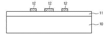
図1に示すように、金属板10の上に絶縁層11が形成される。
As shown in FIG. 1, an
絶縁層11は、樹脂層(resin layer)で形成されることができ、例えば上記樹脂層としてガラスエポキシ系材質であるFR4樹脂層が使われることができる。
The
金属板10は、Al、Auなどのように熱伝導性が優れる金属材質で、数mm乃至数十mmの厚みで形成され、ヒットシンク(heat sink)としての役割をすることになる。
The
絶縁層11は、機械的強度が高く、かつ耐久性が優れるので、薄い厚みでなされた場合にも熱による変形が小さいし、接着性があるので、レイヤーを形成するに適したFR4樹脂層が使われる。
Since the insulating
一方、絶縁層11は、プレスまたは熱圧搾ジグ(jig)を利用して金属板10の上部面に形成することができ、プレスまたは熱圧搾ジグにより加えられる熱により金属板10に接着されることができる。
On the other hand, the
図2に示すように、絶縁層11の上側に回路パターン12を形成する。
As shown in FIG. 2, a
回路パターン12は、銅のような金属材質を使用して形成する。回路パターン12は、半導体回路の形成のための工程技術、例えば、光リソグラフィー(photo-lithography)、メタライゼーション(metallization)、エッチングなどの方法を利用して形成することができる。
The
したがって、図1と図2に示すように、回路パターン12が形成されたMCPCBが準備される。
Therefore, as shown in FIGS. 1 and 2, the MCPCB on which the
図3を参照すれば、絶縁層11の上側に選択的に反射膜13を形成する。
Referring to FIG. 3, the
反射膜13は、コーティング方法により形成されることができ、回路パターン12が形成されない領域の絶縁層11の上側に形成されることができる。
The
反射膜13は、発光ダイオードチップから放出される光の輝度を増大させるためのものであって、発光ダイオードチップが装着される領域及び回路パターン12が形成される領域を考慮して絶縁層11の上側に適切に形成する。
The
反射膜13は、酸化チタンと樹脂を主成分とし、炭酸カルシウム、硫酸バリウム及び酸化亜鉛のうち、少なくとも1つを混合したホワイト樹脂が使われることができる。勿論、ホワイト樹脂の以外に白色顔料を用いて反射膜13を形成することができる。
The
図3では、回路パターン12と回路パターン12との間には反射膜13が形成されなかったが、選択によって回路パターン12と回路パターン12との間にも反射膜を形成することができる。
In FIG. 3, the
上記ホワイト樹脂を反射膜13で形成するために、空圧方式のディスペンシング(Dispensing)方式でない、スクリーンプリンティング(Screen Printing)方式を使用する。
In order to form the white resin with the
上記スクリーンプリンティング方式は、空圧方式のディスペンシング方式に比べて短い時間の間、多くの面積にホワイト樹脂を塗布することができるので、設備投資費用が少ない。 The screen printing method can apply a white resin over a large area in a short time compared to the pneumatic dispensing method, and therefore the equipment investment cost is low.
上記スクリーンプリンティング方式は、回路パターン12の上に厚みが50?であるスクリーンマスクを形成し、スクイズ(squeeze)を利用してスクリーンマスクの以外の部分にホワイト樹脂を詰める。
In the screen printing method, a screen mask having a thickness of 50? Is formed on the
具体的に、スクイズはスクリーンマスクの上側面に沿って既設定された方向に液状のホワイト樹脂を擦りながら移動し、液状のホワイト樹脂はスクリーンマスクの以外の部分に詰められる。 Specifically, the squeeze moves while rubbing the liquid white resin in a predetermined direction along the upper surface of the screen mask, and the liquid white resin is packed in a portion other than the screen mask.
スクリーンマスクの以外の部分に液状のホワイト樹脂が詰められてホワイト樹脂の表面がスクリーンマスクの上部表面と同一に平らになるようにする。そして、上記スクリーンマスクを除去し、既設定された温度でアニーリングを遂行してホワイト樹脂が硬化されるようにする。 A portion other than the screen mask is filled with liquid white resin so that the surface of the white resin is flush with the upper surface of the screen mask. Then, the screen mask is removed, and the white resin is cured by performing annealing at a preset temperature.
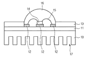
図4に示すように、上記ホワイト樹脂からなる反射膜13を形成した後、発光ダイオードチップ14をMCPCBの上に実装する。
As shown in FIG. 4, after the
具体的に、発光ダイオードチップ14を回路パターン12に装着し、ワイヤー15を利用して発光ダイオードチップ14と回路パターン12を電気的に連結する。そして、発光ダイオードチップ14及びワイヤー15にモールディング部16を形成する。
Specifically, the light
発光ダイオードチップ14は絶縁層11の上に形成されることができ、反射膜13の上に形成されることもできる。
The light
一方、発光ダイオードチップ14は、SiOB(Silicon Optical Bench:シリコン光学ベンチ)にフリップボンディングして実装されることができ、発光ダイオードチップ14がフリップボンディングされたSiOBを熱伝導性を有したペーストを利用して絶縁層11の上に装着してリードフレームを利用して回路パターン12と電気的に連結されるようにすることができる。
On the other hand, the light-emitting
発光ダイオードチップ14をMCPCBに実装した後、金属板10、絶縁層11及び反射膜13を選択的に除去して、金属板10の上側面に複数の溝17を形成する。
After mounting the light
溝17の上側には絶縁層11及び反射膜13が除去されるため、溝17の底面及び側面は空気中に露出される。したがって、金属板10の放熱効果を極大化することができる。
Since the
一方、溝17が形成された後、発光ダイオードチップ14がMCPCBに実装されることもできる。
On the other hand, the light
ここで、上記複数の溝17は、ドリリングマシン、またはミーリングマシンを利用した機械的方法により形成されるか、エッチング方法を利用した化学的方法により形成されることができる。
Here, the plurality of
したがって、本発明による発光ダイオードパッケージは、複数の溝17により放熱のための金属板10の断面積が広くなることにより、発光ダイオードチップ14などから発生する熱が効果的に放熱されることができる。したがって、発光ダイオードチップ14に対する熱的信頼性を向上させることができるので、発光ダイオードチップ14の性能を向上させることができる。
Therefore, in the light emitting diode package according to the present invention, the heat generated from the light
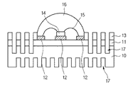
図5は、本発明の他の実施形態による発光ダイオードパッケージを説明するための図である。 FIG. 5 is a view illustrating a light emitting diode package according to another embodiment of the present invention.
図5に図示された発光ダイオードパッケージは、図4に図示された発光ダイオードパッケージとは異なり、複数の溝17が金属板の下側面に形成される。
Unlike the light emitting diode package illustrated in FIG. 4, the light emitting diode package illustrated in FIG. 5 has a plurality of
したがって、反射膜13が形成された面積が増加されて光効率がより向上することができ、溝17の個数も増加されて放熱効果が極大化されることができる。
Therefore, the area on which the
図6は、本発明の更に他の実施形態による発光ダイオードパッケージを説明するための図である。 FIG. 6 is a view illustrating a light emitting diode package according to another embodiment of the present invention.
図6に図示された発光ダイオードパッケージは、図4及び図5に図示された発光ダイオードパッケージとは異なり、複数の溝17が金属板10の上側面及び下側面に形成される。
The light emitting diode package illustrated in FIG. 6 is different from the light emitting diode package illustrated in FIGS. 4 and 5 in that a plurality of
したがって、複数の溝17による放熱効果が極大化されることができる。
Therefore, the heat dissipation effect by the plurality of
一方、金属板10の上側面に形成された溝17と下側面に形成された溝17の位置が互いに相異するように形成する。即ち、金属板10の上側面に形成された溝17の下側には溝17を形成せず、金属板10の上側面に溝17が形成されない部分の下側に溝17を形成する。
On the other hand, the
言い換えると、金属板10の上側面に形成された溝17と下側面に形成された溝17は同一垂直線上に形成されない。
In other words, the
これによって、金属板10の機械的強度が維持されることができる。
Thereby, the mechanical strength of the
本実施形態では、発光ダイオードチップが実装された発光ダイオードパッケージを説明したが、IC、抵抗など、その他の電子素子が装着されたMCPCBにも適用されることができる。 In this embodiment, the light emitting diode package on which the light emitting diode chip is mounted has been described. However, the present invention can also be applied to an MCPCB on which other electronic elements such as an IC and a resistor are mounted.
本発明は、電子素子が装着された回路基板に適用されることができる。 The present invention can be applied to a circuit board on which an electronic element is mounted.
Claims (20)
前記金属板の上の絶縁層と、
前記絶縁層の上の回路パターンと、
前記絶縁層上の反射膜と、
前記回路パターンと電気的に連結された前記絶縁層の上の発光ダイオードと、を備え、
前記発光ダイオードは、前記発光ダイオードに最も近い2つの溝に挟まれた部分に設置されており、前記反射膜の一部が前記発光ダイオードに最も近い2つの溝に挟まれた部分に形成されていることを特徴とする発光ダイオードパッケージ。 A metal plate with grooves formed on the upper surface;
An insulating layer on the metal plate;
A circuit pattern on the insulating layer;
A reflective film on the insulating layer ;
A light emitting diode on the insulating layer electrically connected to the circuit pattern,
The light emitting diode is installed in a portion sandwiched between two grooves closest to the light emitting diode, and a part of the reflective film is formed in a portion sandwiched between two grooves closest to the light emitting diode. A light emitting diode package characterized by comprising:
前記MCPCBの上に反射膜を形成する段階と、
前記MCPCBに含まれた金属板および前記反射膜を選択的に除去して前記MCPCBの上側面に溝を形成する段階と、
前記MCPCBの上に発光ダイオードを実装する段階と、
を含み、
前記発光ダイオードは、前記発光ダイオードに最も近い2つの溝に挟まれた部分に設置されており、前記反射膜の一部が前記発光ダイオードに最も近い2つの溝に挟まれた部分に形成されていることを特徴とする発光ダイオードパッケージの製造方法。 Preparing a metal plate, an insulating layer on the metal plate, and an MCPCB (Metal Core Printed Circuit Board) having a circuit pattern on the insulating layer ;
Forming a reflective film on the MCPCB;
Selectively removing the metal plate and the reflective film included in the MCPCB to form a groove on the upper surface of the MCPCB;
Mounting a light emitting diode on the MCPCB;
Including
The light emitting diode is installed in a portion sandwiched between two grooves closest to the light emitting diode, and a part of the reflective film is formed in a portion sandwiched between two grooves closest to the light emitting diode. A method for manufacturing a light emitting diode package, comprising:
造方法。 2. The reflective film according to claim 1, wherein a white resin formed by mixing at least one of calcium carbonate, barium sulfate, and zinc oxide is formed by a screen printing method. 10. A method for producing a light emitting diode package according to 9.
前記金属板の上の絶縁層と、
前記絶縁層の上の回路パターンと、
前記絶縁層上の反射膜と、
前記絶縁層の上の前記回路パターンと電気的に連結された電子素子と、
を備え、
前記電子素子は、前記電子素子に最も近い2つの溝に挟まれた部分に設置されており、前記反射膜の一部が前記電子素子に最も近い2つの溝に挟まれた部分に形成されていることを特徴とする装置。 A metal plate with grooves formed on the upper surface side;
An insulating layer on the metal plate;
A circuit pattern on the insulating layer;
A reflective film on the insulating layer ;
An electronic device electrically connected to the circuit pattern on the insulating layer;
With
The electronic element is installed in a part sandwiched between two grooves closest to the electronic element, and a part of the reflective film is formed in a part sandwiched between two grooves closest to the electronic element. A device characterized by comprising.
た溝と下側面に形成された溝は同一垂直線上に形成されないことを特徴とする請求項17記載の装置。 The groove is formed on both an upper surface and a lower surface of the metal plate, and the groove formed on the upper surface and the groove formed on the lower surface are not formed on the same vertical line. The apparatus of claim 17.
Applications Claiming Priority (3)
| Application Number | Priority Date | Filing Date | Title |
|---|---|---|---|
| KR1020060020305A KR101210090B1 (en) | 2006-03-03 | 2006-03-03 | Metal core printed circuit board and light-emitting diode packaging method thereof |
| KR10-2006-0020305 | 2006-03-03 | ||
| PCT/KR2007/001020 WO2007100209A1 (en) | 2006-03-03 | 2007-02-28 | Light-emitting diode package and manufacturing method thereof |
Related Child Applications (1)
| Application Number | Title | Priority Date | Filing Date |
|---|---|---|---|
| JP2012095306A Division JP5759413B2 (en) | 2006-03-03 | 2012-04-19 | Light emitting diode package |
Publications (3)
| Publication Number | Publication Date |
|---|---|
| JP2009528695A JP2009528695A (en) | 2009-08-06 |
| JP2009528695A5 JP2009528695A5 (en) | 2010-01-14 |
| JP5323501B2 true JP5323501B2 (en) | 2013-10-23 |
Family
ID=38459278
Family Applications (2)
| Application Number | Title | Priority Date | Filing Date |
|---|---|---|---|
| JP2008557208A Active JP5323501B2 (en) | 2006-03-03 | 2007-02-28 | Light emitting diode package and manufacturing method thereof |
| JP2012095306A Active JP5759413B2 (en) | 2006-03-03 | 2012-04-19 | Light emitting diode package |
Family Applications After (1)
| Application Number | Title | Priority Date | Filing Date |
|---|---|---|---|
| JP2012095306A Active JP5759413B2 (en) | 2006-03-03 | 2012-04-19 | Light emitting diode package |
Country Status (6)
| Country | Link |
|---|---|
| US (3) | US7745844B2 (en) |
| JP (2) | JP5323501B2 (en) |
| KR (1) | KR101210090B1 (en) |
| CN (1) | CN101213892B (en) |
| TW (1) | TWI429100B (en) |
| WO (1) | WO2007100209A1 (en) |
Families Citing this family (28)
| Publication number | Priority date | Publication date | Assignee | Title |
|---|---|---|---|---|
| KR101210090B1 (en) * | 2006-03-03 | 2012-12-07 | 엘지이노텍 주식회사 | Metal core printed circuit board and light-emitting diode packaging method thereof |
| WO2010021089A1 (en) * | 2008-08-21 | 2010-02-25 | パナソニック株式会社 | Light source for lighting |
| KR101134555B1 (en) * | 2009-03-23 | 2012-04-16 | 금호전기주식회사 | Printed circuit board for setting light emitting device |
| KR101124102B1 (en) * | 2009-08-24 | 2012-03-21 | 삼성전기주식회사 | Substrate for light emitting device package and light emitting device package comprising the same |
| KR20110068689A (en) * | 2009-12-16 | 2011-06-22 | 삼성전기주식회사 | Package substrate for optical element and manufacturing method thereof |
| US8616732B2 (en) * | 2010-02-12 | 2013-12-31 | Toshiba Lighting & Technology Corporation | Light-emitting device and illumination device |
| KR101121151B1 (en) * | 2010-03-19 | 2012-03-20 | 주식회사 대원이노스트 | Led module and fabrication method of thereof |
| KR101037168B1 (en) * | 2010-06-04 | 2011-05-26 | 지성수 | Printed circuit board and manufacturing method thereof |
| KR101101709B1 (en) * | 2010-12-16 | 2012-01-05 | 한국세라믹기술원 | Led array heat-radiating module and manufacturing method thereof |
| KR101166066B1 (en) | 2010-12-21 | 2012-07-19 | 주식회사 루셈 | Light Emitting Diode Package |
| KR101775428B1 (en) * | 2010-12-28 | 2017-09-06 | 삼성전자 주식회사 | Light emitting device package and method of manufacturing the same |
| CN102104092A (en) * | 2011-01-13 | 2011-06-22 | 北京易光天元半导体照明科技有限公司 | Novel LED encapsulation method and device beneficial to radiating |
| EP2668442B1 (en) * | 2011-01-25 | 2016-05-25 | Koninklijke Philips N.V. | Led-based modular assembly |
| TWI419270B (en) * | 2011-03-24 | 2013-12-11 | Chipmos Technologies Inc | Package on package structure |
| TW201347244A (en) * | 2012-05-10 | 2013-11-16 | Gem Weltronics Twn Corp | Integrated high efficiency multi-layer lighting device |
| KR101236715B1 (en) * | 2012-08-28 | 2013-02-25 | 주식회사 썬엘이디 | Production method of led module including chip on board dam using silicon molding type and led module by the production method |
| JP5784658B2 (en) * | 2013-02-28 | 2015-09-24 | 株式会社東芝 | Semiconductor device manufacturing method and manufacturing apparatus |
| EP2806211A1 (en) * | 2013-05-21 | 2014-11-26 | OSRAM GmbH | Solid-state lighting device and related process |
| KR101592649B1 (en) * | 2013-12-24 | 2016-02-12 | 현대자동차주식회사 | Laser optical system for head lamp |
| CN104613379B (en) * | 2015-02-06 | 2017-12-26 | 东莞佰鸿电子有限公司 | A kind of sapphire printed circuit board (PCB) LED lamp and preparation method thereof |
| CN105655472A (en) * | 2016-02-02 | 2016-06-08 | 上海鼎晖科技股份有限公司 | COB (Chip On Board) LED (Light Emitting Diode) light source with metal heat-conducting columns |
| CN106449563B (en) * | 2016-11-29 | 2018-11-13 | 卡姆丹克太阳能(江苏)有限公司 | A kind of wafer level packaging with fin structure |
| CN106449443B (en) * | 2016-11-29 | 2019-01-01 | 海安浩驰科技有限公司 | A kind of wafer packaging method with fin structure |
| DE102019126021A1 (en) * | 2019-09-26 | 2021-04-01 | OSRAM Opto Semiconductors Gesellschaft mit beschränkter Haftung | OPTOELECTRONIC SEMICONDUCTOR COMPONENT AND METHOD FOR MANUFACTURING AN OPTOELECTRONIC SEMICONDUCTOR COMPONENT |
| CN111048651B (en) * | 2019-12-27 | 2021-12-17 | 广州市鸿利秉一光电科技有限公司 | High-reflectivity UVLED substrate and production method |
| US11894357B2 (en) * | 2020-09-10 | 2024-02-06 | Sj Semiconductor (Jiangyin) Corporation | System-level packaging structure and method for LED chip |
| WO2023133720A1 (en) * | 2022-01-12 | 2023-07-20 | 谢华棣 | Manufacturing method for circuit board assembly having three-dimensional heat dissipation |
| US20240074031A1 (en) * | 2022-08-29 | 2024-02-29 | Creeled, Inc. | Textured metal core printed circuit boards for improved thermal dissipation |
Family Cites Families (44)
| Publication number | Priority date | Publication date | Assignee | Title |
|---|---|---|---|---|
| JPS6028366U (en) * | 1983-08-03 | 1985-02-26 | 昭和アルミニウム株式会社 | Condenser |
| JPH0416468Y2 (en) * | 1986-07-31 | 1992-04-13 | ||
| JPH0677540A (en) * | 1992-08-24 | 1994-03-18 | Sanyo Electric Co Ltd | Optical semiconductor device |
| JPH08204294A (en) * | 1995-01-27 | 1996-08-09 | Fuji Electric Co Ltd | Printed wiring board integrated with heat radiating fin |
| US5739554A (en) * | 1995-05-08 | 1998-04-14 | Cree Research, Inc. | Double heterojunction light emitting diode with gallium nitride active layer |
| JPH10144963A (en) * | 1996-11-05 | 1998-05-29 | Sanyo Electric Co Ltd | Led light source and its manufacture |
| JPH11284110A (en) * | 1998-03-30 | 1999-10-15 | Onkyo Corp | Fitting structure of power transistor in heat sink |
| JP3605547B2 (en) * | 1999-06-11 | 2004-12-22 | 松下電器産業株式会社 | Heat dissipating substrate and manufacturing method thereof |
| JP3640153B2 (en) * | 1999-11-18 | 2005-04-20 | 松下電工株式会社 | Illumination light source |
| TW507482B (en) * | 2000-06-09 | 2002-10-21 | Sanyo Electric Co | Light emitting device, its manufacturing process, and lighting device using such a light-emitting device |
| JP3602453B2 (en) * | 2000-08-31 | 2004-12-15 | Necエレクトロニクス株式会社 | Semiconductor device |
| JP3472252B2 (en) * | 2000-09-07 | 2003-12-02 | 日本リークレス工業株式会社 | Method for manufacturing expanded graphite heat sink |
| US6906455B2 (en) * | 2001-02-26 | 2005-06-14 | Sony Corporation | Transfer foil, transfer method, transfer apparatus, flat cathode-ray tube, and its manufacturing method |
| JP2003249675A (en) * | 2002-02-26 | 2003-09-05 | Sumitomo Electric Ind Ltd | Light receiving element array |
| JP2003304000A (en) | 2002-04-08 | 2003-10-24 | Citizen Electronics Co Ltd | Method for manufacturing package for light-emitting diode |
| JP3838164B2 (en) * | 2002-06-18 | 2006-10-25 | 住友電気工業株式会社 | Optical communication element and method for manufacturing optical communication element |
| JP3655267B2 (en) * | 2002-07-17 | 2005-06-02 | 株式会社東芝 | Semiconductor light emitting device |
| TW578280B (en) * | 2002-11-21 | 2004-03-01 | United Epitaxy Co Ltd | Light emitting diode and package scheme and method thereof |
| US7420271B2 (en) * | 2003-02-20 | 2008-09-02 | Tsung Hsin Chen | Heat conductivity and brightness enhancing structure for light-emitting diode |
| JP2004319530A (en) * | 2003-02-28 | 2004-11-11 | Sanyo Electric Co Ltd | Optical semiconductor device and its manufacturing process |
| TW560813U (en) * | 2003-03-06 | 2003-11-01 | Shang-Hua You | Improved LED seat |
| TW594950B (en) * | 2003-03-18 | 2004-06-21 | United Epitaxy Co Ltd | Light emitting diode and package scheme and method thereof |
| US6864513B2 (en) * | 2003-05-07 | 2005-03-08 | Kaylu Industrial Corporation | Light emitting diode bulb having high heat dissipating efficiency |
| WO2004105142A1 (en) * | 2003-05-26 | 2004-12-02 | Matsushita Electric Works, Ltd. | Light-emitting device |
| KR100524656B1 (en) | 2003-09-30 | 2005-10-31 | 서울반도체 주식회사 | Polychromatic Light Emitting Diode Package and Polychromatic Light Emitting Diode System |
| JP4966656B2 (en) | 2003-05-28 | 2012-07-04 | ソウル半導体株式会社 | Light emitting diode package with multiple heat sinks |
| KR100455089B1 (en) | 2003-05-28 | 2004-11-06 | 서울반도체 주식회사 | Package for high-power semiconductor light emitting devices and semiconductor light emitting device using the same |
| US6983086B2 (en) * | 2003-06-19 | 2006-01-03 | Intel Corporation | Thermally isolating optical devices |
| JP4254470B2 (en) * | 2003-10-10 | 2009-04-15 | 豊田合成株式会社 | Light emitting device |
| JP2005056653A (en) * | 2003-08-01 | 2005-03-03 | Fuji Photo Film Co Ltd | Light source device |
| JP4400327B2 (en) * | 2003-09-11 | 2010-01-20 | セイコーエプソン株式会社 | Wiring formation method for tile-shaped element |
| US20050077616A1 (en) * | 2003-10-09 | 2005-04-14 | Ng Kee Yean | High power light emitting diode device |
| JP2005217147A (en) * | 2004-01-29 | 2005-08-11 | Seiko Epson Corp | Light receiving and emitting element array, optical module, and optical transmission device |
| US20050199899A1 (en) | 2004-03-11 | 2005-09-15 | Ming-Der Lin | Package array and package unit of flip chip LED |
| CN1708212A (en) * | 2004-06-11 | 2005-12-14 | 周明庆 | Heat conductive substrate apparatus |
| US7745832B2 (en) * | 2004-09-24 | 2010-06-29 | Epistar Corporation | Semiconductor light-emitting element assembly with a composite substrate |
| US20060097385A1 (en) * | 2004-10-25 | 2006-05-11 | Negley Gerald H | Solid metal block semiconductor light emitting device mounting substrates and packages including cavities and heat sinks, and methods of packaging same |
| US20060124953A1 (en) * | 2004-12-14 | 2006-06-15 | Negley Gerald H | Semiconductor light emitting device mounting substrates and packages including cavities and cover plates, and methods of packaging same |
| JP4618682B2 (en) | 2005-01-28 | 2011-01-26 | 株式会社神戸製鋼所 | High strength spring steel with excellent hydrogen embrittlement resistance |
| US7411225B2 (en) * | 2005-03-21 | 2008-08-12 | Lg Electronics Inc. | Light source apparatus |
| KR100592508B1 (en) * | 2005-07-15 | 2006-06-26 | 한국광기술원 | High power led package with beacon type substrate |
| TWI280332B (en) * | 2005-10-31 | 2007-05-01 | Guei-Fang Chen | LED lighting device |
| KR101210090B1 (en) * | 2006-03-03 | 2012-12-07 | 엘지이노텍 주식회사 | Metal core printed circuit board and light-emitting diode packaging method thereof |
| US20080175003A1 (en) * | 2007-01-22 | 2008-07-24 | Cheng Home Electronics Co., Ltd. | Led sunken lamp |
-
2006
- 2006-03-03 KR KR1020060020305A patent/KR101210090B1/en active IP Right Grant
-
2007
- 2007-02-28 WO PCT/KR2007/001020 patent/WO2007100209A1/en active Application Filing
- 2007-02-28 US US11/910,174 patent/US7745844B2/en active Active
- 2007-02-28 CN CN2007800000705A patent/CN101213892B/en active Active
- 2007-02-28 JP JP2008557208A patent/JP5323501B2/en active Active
- 2007-03-02 TW TW096107087A patent/TWI429100B/en active
-
2010
- 2010-05-26 US US12/788,090 patent/US8212274B2/en not_active Expired - Fee Related
-
2012
- 2012-04-19 JP JP2012095306A patent/JP5759413B2/en active Active
- 2012-06-13 US US13/495,664 patent/US8796717B2/en active Active
Also Published As
| Publication number | Publication date |
|---|---|
| US20080179612A1 (en) | 2008-07-31 |
| WO2007100209A1 (en) | 2007-09-07 |
| US20100230707A1 (en) | 2010-09-16 |
| US7745844B2 (en) | 2010-06-29 |
| KR101210090B1 (en) | 2012-12-07 |
| KR20070090509A (en) | 2007-09-06 |
| CN101213892B (en) | 2012-09-05 |
| CN101213892A (en) | 2008-07-02 |
| JP5759413B2 (en) | 2015-08-05 |
| US8212274B2 (en) | 2012-07-03 |
| JP2009528695A (en) | 2009-08-06 |
| US20120248488A1 (en) | 2012-10-04 |
| TWI429100B (en) | 2014-03-01 |
| JP2012178581A (en) | 2012-09-13 |
| TW200735425A (en) | 2007-09-16 |
| US8796717B2 (en) | 2014-08-05 |
Similar Documents
| Publication | Publication Date | Title |
|---|---|---|
| JP5323501B2 (en) | Light emitting diode package and manufacturing method thereof | |
| KR101283182B1 (en) | Package of light-emitting diode and manufacturing method thereof | |
| US8610146B2 (en) | Light emitting diode package and method of manufacturing the same | |
| JP5746877B2 (en) | Power surface mounted light emitting die package | |
| US10667345B2 (en) | Method for manufacturing light-emitting device packages, light-emitting device package strip, and light-emitting device package | |
| EP2479810B1 (en) | Light-emitting device package and method of manufacturing the same | |
| JP5940799B2 (en) | Electronic component mounting package, electronic component package, and manufacturing method thereof | |
| JP2007294506A (en) | Heat dissipation substrate and its manufacturing method, and light emitting module using same, and indicating device | |
| US20150060920A1 (en) | Wiring Substrate and Light Emitting Device | |
| JP5381563B2 (en) | Method for manufacturing lead frame substrate for light emitting device | |
| TW201133729A (en) | Semiconductor chip assembly with post/base heat spreader and conductive trace | |
| JP4923700B2 (en) | Heat dissipation substrate, manufacturing method thereof, light emitting module and display device using the same | |
| KR101273045B1 (en) | Package of light emitting diode | |
| JP2007158211A (en) | Light-emitting module and manufacturing method therefor | |
| JP2007158208A (en) | Light-emitting module and manufacturing method therefor |
Legal Events
| Date | Code | Title | Description |
|---|---|---|---|
| A521 | Request for written amendment filed |
Free format text: JAPANESE INTERMEDIATE CODE: A523 Effective date: 20091117 |
|
| A621 | Written request for application examination |
Free format text: JAPANESE INTERMEDIATE CODE: A621 Effective date: 20091117 |
|
| A977 | Report on retrieval |
Free format text: JAPANESE INTERMEDIATE CODE: A971007 Effective date: 20111130 |
|
| A131 | Notification of reasons for refusal |
Free format text: JAPANESE INTERMEDIATE CODE: A131 Effective date: 20111220 |
|
| A601 | Written request for extension of time |
Free format text: JAPANESE INTERMEDIATE CODE: A601 Effective date: 20120319 |
|
| A602 | Written permission of extension of time |
Free format text: JAPANESE INTERMEDIATE CODE: A602 Effective date: 20120327 |
|
| A521 | Request for written amendment filed |
Free format text: JAPANESE INTERMEDIATE CODE: A523 Effective date: 20120419 |
|
| A131 | Notification of reasons for refusal |
Free format text: JAPANESE INTERMEDIATE CODE: A131 Effective date: 20121002 |
|
| A601 | Written request for extension of time |
Free format text: JAPANESE INTERMEDIATE CODE: A601 Effective date: 20121228 |
|
| A602 | Written permission of extension of time |
Free format text: JAPANESE INTERMEDIATE CODE: A602 Effective date: 20130110 |
|
| A521 | Request for written amendment filed |
Free format text: JAPANESE INTERMEDIATE CODE: A523 Effective date: 20130130 |
|
| TRDD | Decision of grant or rejection written | ||
| A01 | Written decision to grant a patent or to grant a registration (utility model) |
Free format text: JAPANESE INTERMEDIATE CODE: A01 Effective date: 20130702 |
|
| A61 | First payment of annual fees (during grant procedure) |
Free format text: JAPANESE INTERMEDIATE CODE: A61 Effective date: 20130717 |
|
| R150 | Certificate of patent or registration of utility model |
Ref document number: 5323501 Country of ref document: JP Free format text: JAPANESE INTERMEDIATE CODE: R150 Free format text: JAPANESE INTERMEDIATE CODE: R150 |
|
| R250 | Receipt of annual fees |
Free format text: JAPANESE INTERMEDIATE CODE: R250 |
|
| R250 | Receipt of annual fees |
Free format text: JAPANESE INTERMEDIATE CODE: R250 |
|
| R250 | Receipt of annual fees |
Free format text: JAPANESE INTERMEDIATE CODE: R250 |
|
| R250 | Receipt of annual fees |
Free format text: JAPANESE INTERMEDIATE CODE: R250 |
|
| R250 | Receipt of annual fees |
Free format text: JAPANESE INTERMEDIATE CODE: R250 |
|
| R250 | Receipt of annual fees |
Free format text: JAPANESE INTERMEDIATE CODE: R250 |
|
| S531 | Written request for registration of change of domicile |
Free format text: JAPANESE INTERMEDIATE CODE: R313531 |
|
| S111 | Request for change of ownership or part of ownership |
Free format text: JAPANESE INTERMEDIATE CODE: R313113 |
|
| R350 | Written notification of registration of transfer |
Free format text: JAPANESE INTERMEDIATE CODE: R350 |
|
| R350 | Written notification of registration of transfer |
Free format text: JAPANESE INTERMEDIATE CODE: R350 |
|
| R250 | Receipt of annual fees |
Free format text: JAPANESE INTERMEDIATE CODE: R250 |
|
| R250 | Receipt of annual fees |
Free format text: JAPANESE INTERMEDIATE CODE: R250 |