JP5259572B2 - Liquid crystal display - Google Patents
Liquid crystal display Download PDFInfo
- Publication number
- JP5259572B2 JP5259572B2 JP2009504013A JP2009504013A JP5259572B2 JP 5259572 B2 JP5259572 B2 JP 5259572B2 JP 2009504013 A JP2009504013 A JP 2009504013A JP 2009504013 A JP2009504013 A JP 2009504013A JP 5259572 B2 JP5259572 B2 JP 5259572B2
- Authority
- JP
- Japan
- Prior art keywords
- subpixel
- liquid crystal
- display device
- crystal display
- pixel
- Prior art date
- Legal status (The legal status is an assumption and is not a legal conclusion. Google has not performed a legal analysis and makes no representation as to the accuracy of the status listed.)
- Expired - Fee Related
Links
- 239000004973 liquid crystal related substance Substances 0.000 title claims description 534
- 239000003990 capacitor Substances 0.000 claims description 538
- 235000019557 luminance Nutrition 0.000 claims description 47
- 238000003860 storage Methods 0.000 claims description 8
- 239000000463 material Substances 0.000 claims description 5
- 239000011159 matrix material Substances 0.000 claims description 5
- 238000000605 extraction Methods 0.000 claims 1
- 102000007620 Pulmonary Surfactant-Associated Protein C Human genes 0.000 description 192
- 108010007125 Pulmonary Surfactant-Associated Protein C Proteins 0.000 description 192
- 102100027773 Pulmonary surfactant-associated protein A2 Human genes 0.000 description 154
- 108010007100 Pulmonary Surfactant-Associated Protein A Proteins 0.000 description 153
- DZRJLJPPUJADOO-UHFFFAOYSA-N chaetomin Natural products CN1C(=O)C2(Cc3cn(C)c4ccccc34)SSC1(CO)C(=O)N2C56CC78SSC(CO)(N(C)C7=O)C(=O)N8C5Nc9ccccc69 DZRJLJPPUJADOO-UHFFFAOYSA-N 0.000 description 61
- DIUIQJFZKRAGBZ-UHFFFAOYSA-N chetoseminudin A Natural products O=C1C(SSS2)(CO)N(C)C(=O)C32CC2(N4C5=CC=CC=C5C(CC56C(N(C)C(CO)(SS5)C(=O)N6C)=O)=C4)C4=CC=CC=C4NC2N31 DIUIQJFZKRAGBZ-UHFFFAOYSA-N 0.000 description 59
- 239000000758 substrate Substances 0.000 description 45
- 102100027845 Pulmonary surfactant-associated protein D Human genes 0.000 description 44
- 230000009471 action Effects 0.000 description 41
- 239000010410 layer Substances 0.000 description 37
- 101100383992 Arabidopsis thaliana CLC-C gene Proteins 0.000 description 33
- 230000003071 parasitic effect Effects 0.000 description 33
- -1 SP-B Proteins 0.000 description 32
- 101100328110 Arabidopsis thaliana CLC-A gene Proteins 0.000 description 31
- 101100496126 Arabidopsis thaliana CLC-B gene Proteins 0.000 description 31
- 239000010408 film Substances 0.000 description 20
- 230000008859 change Effects 0.000 description 11
- 230000007423 decrease Effects 0.000 description 11
- 238000000034 method Methods 0.000 description 11
- 238000010586 diagram Methods 0.000 description 10
- 239000011229 interlayer Substances 0.000 description 10
- 101100383994 Arabidopsis thaliana CLC-D gene Proteins 0.000 description 9
- 101150089829 csc-1 gene Proteins 0.000 description 9
- 239000002131 composite material Substances 0.000 description 6
- 238000007667 floating Methods 0.000 description 5
- 238000004519 manufacturing process Methods 0.000 description 5
- 230000001747 exhibiting effect Effects 0.000 description 4
- 230000006870 function Effects 0.000 description 4
- 239000002184 metal Substances 0.000 description 4
- 230000008569 process Effects 0.000 description 4
- 230000001105 regulatory effect Effects 0.000 description 4
- 239000003086 colorant Substances 0.000 description 3
- 230000008878 coupling Effects 0.000 description 3
- 238000010168 coupling process Methods 0.000 description 3
- 238000005859 coupling reaction Methods 0.000 description 3
- 230000006866 deterioration Effects 0.000 description 3
- 230000000694 effects Effects 0.000 description 3
- 230000004048 modification Effects 0.000 description 3
- 238000012986 modification Methods 0.000 description 3
- 230000010287 polarization Effects 0.000 description 3
- 238000000926 separation method Methods 0.000 description 3
- CCPHAMSKHBDMDS-UHFFFAOYSA-N Chetoseminudin B Natural products C=1NC2=CC=CC=C2C=1CC1(SC)NC(=O)C(CO)(SC)N(C)C1=O CCPHAMSKHBDMDS-UHFFFAOYSA-N 0.000 description 2
- 238000013459 approach Methods 0.000 description 2
- 230000002238 attenuated effect Effects 0.000 description 2
- 238000000576 coating method Methods 0.000 description 2
- 239000000284 extract Substances 0.000 description 2
- 238000009499 grossing Methods 0.000 description 2
- 230000004044 response Effects 0.000 description 2
- 239000004065 semiconductor Substances 0.000 description 2
- 230000003068 static effect Effects 0.000 description 2
- 239000004925 Acrylic resin Substances 0.000 description 1
- 229920000178 Acrylic resin Polymers 0.000 description 1
- 101000864780 Homo sapiens Pulmonary surfactant-associated protein A1 Proteins 0.000 description 1
- 101000651017 Homo sapiens Pulmonary surfactant-associated protein A2 Proteins 0.000 description 1
- 239000004988 Nematic liquid crystal Substances 0.000 description 1
- 108010007127 Pulmonary Surfactant-Associated Protein D Proteins 0.000 description 1
- 102100030060 Pulmonary surfactant-associated protein A1 Human genes 0.000 description 1
- 230000001174 ascending effect Effects 0.000 description 1
- 230000008901 benefit Effects 0.000 description 1
- 230000005540 biological transmission Effects 0.000 description 1
- 230000015556 catabolic process Effects 0.000 description 1
- 238000006243 chemical reaction Methods 0.000 description 1
- 239000011248 coating agent Substances 0.000 description 1
- 239000000470 constituent Substances 0.000 description 1
- 238000006731 degradation reaction Methods 0.000 description 1
- 239000006185 dispersion Substances 0.000 description 1
- 238000009826 distribution Methods 0.000 description 1
- 230000005684 electric field Effects 0.000 description 1
- 238000005516 engineering process Methods 0.000 description 1
- 230000006872 improvement Effects 0.000 description 1
- 238000003780 insertion Methods 0.000 description 1
- 230000037431 insertion Effects 0.000 description 1
- 230000007257 malfunction Effects 0.000 description 1
- 230000010355 oscillation Effects 0.000 description 1
- 238000012545 processing Methods 0.000 description 1
- 230000009467 reduction Effects 0.000 description 1
- 239000011347 resin Substances 0.000 description 1
- 229920005989 resin Polymers 0.000 description 1
- 239000010409 thin film Substances 0.000 description 1
- 238000002834 transmittance Methods 0.000 description 1
- 238000007740 vapor deposition Methods 0.000 description 1
Images


Classifications
-
- G—PHYSICS
- G02—OPTICS
- G02F—OPTICAL DEVICES OR ARRANGEMENTS FOR THE CONTROL OF LIGHT BY MODIFICATION OF THE OPTICAL PROPERTIES OF THE MEDIA OF THE ELEMENTS INVOLVED THEREIN; NON-LINEAR OPTICS; FREQUENCY-CHANGING OF LIGHT; OPTICAL LOGIC ELEMENTS; OPTICAL ANALOGUE/DIGITAL CONVERTERS
- G02F1/00—Devices or arrangements for the control of the intensity, colour, phase, polarisation or direction of light arriving from an independent light source, e.g. switching, gating or modulating; Non-linear optics
- G02F1/01—Devices or arrangements for the control of the intensity, colour, phase, polarisation or direction of light arriving from an independent light source, e.g. switching, gating or modulating; Non-linear optics for the control of the intensity, phase, polarisation or colour
- G02F1/13—Devices or arrangements for the control of the intensity, colour, phase, polarisation or direction of light arriving from an independent light source, e.g. switching, gating or modulating; Non-linear optics for the control of the intensity, phase, polarisation or colour based on liquid crystals, e.g. single liquid crystal display cells
- G02F1/133—Constructional arrangements; Operation of liquid crystal cells; Circuit arrangements
- G02F1/136—Liquid crystal cells structurally associated with a semi-conducting layer or substrate, e.g. cells forming part of an integrated circuit
- G02F1/1362—Active matrix addressed cells
- G02F1/136213—Storage capacitors associated with the pixel electrode
-
- G—PHYSICS
- G09—EDUCATION; CRYPTOGRAPHY; DISPLAY; ADVERTISING; SEALS
- G09G—ARRANGEMENTS OR CIRCUITS FOR CONTROL OF INDICATING DEVICES USING STATIC MEANS TO PRESENT VARIABLE INFORMATION
- G09G3/00—Control arrangements or circuits, of interest only in connection with visual indicators other than cathode-ray tubes
- G09G3/20—Control arrangements or circuits, of interest only in connection with visual indicators other than cathode-ray tubes for presentation of an assembly of a number of characters, e.g. a page, by composing the assembly by combination of individual elements arranged in a matrix no fixed position being assigned to or needed to be assigned to the individual characters or partial characters
- G09G3/34—Control arrangements or circuits, of interest only in connection with visual indicators other than cathode-ray tubes for presentation of an assembly of a number of characters, e.g. a page, by composing the assembly by combination of individual elements arranged in a matrix no fixed position being assigned to or needed to be assigned to the individual characters or partial characters by control of light from an independent source
- G09G3/36—Control arrangements or circuits, of interest only in connection with visual indicators other than cathode-ray tubes for presentation of an assembly of a number of characters, e.g. a page, by composing the assembly by combination of individual elements arranged in a matrix no fixed position being assigned to or needed to be assigned to the individual characters or partial characters by control of light from an independent source using liquid crystals
- G09G3/3611—Control of matrices with row and column drivers
- G09G3/3648—Control of matrices with row and column drivers using an active matrix
-
- G—PHYSICS
- G02—OPTICS
- G02F—OPTICAL DEVICES OR ARRANGEMENTS FOR THE CONTROL OF LIGHT BY MODIFICATION OF THE OPTICAL PROPERTIES OF THE MEDIA OF THE ELEMENTS INVOLVED THEREIN; NON-LINEAR OPTICS; FREQUENCY-CHANGING OF LIGHT; OPTICAL LOGIC ELEMENTS; OPTICAL ANALOGUE/DIGITAL CONVERTERS
- G02F1/00—Devices or arrangements for the control of the intensity, colour, phase, polarisation or direction of light arriving from an independent light source, e.g. switching, gating or modulating; Non-linear optics
- G02F1/01—Devices or arrangements for the control of the intensity, colour, phase, polarisation or direction of light arriving from an independent light source, e.g. switching, gating or modulating; Non-linear optics for the control of the intensity, phase, polarisation or colour
- G02F1/13—Devices or arrangements for the control of the intensity, colour, phase, polarisation or direction of light arriving from an independent light source, e.g. switching, gating or modulating; Non-linear optics for the control of the intensity, phase, polarisation or colour based on liquid crystals, e.g. single liquid crystal display cells
- G02F1/133—Constructional arrangements; Operation of liquid crystal cells; Circuit arrangements
- G02F1/1333—Constructional arrangements; Manufacturing methods
- G02F1/1343—Electrodes
- G02F1/134309—Electrodes characterised by their geometrical arrangement
- G02F1/134345—Subdivided pixels, e.g. for grey scale or redundancy
-
- G—PHYSICS
- G09—EDUCATION; CRYPTOGRAPHY; DISPLAY; ADVERTISING; SEALS
- G09G—ARRANGEMENTS OR CIRCUITS FOR CONTROL OF INDICATING DEVICES USING STATIC MEANS TO PRESENT VARIABLE INFORMATION
- G09G2300/00—Aspects of the constitution of display devices
- G09G2300/04—Structural and physical details of display devices
- G09G2300/0439—Pixel structures
- G09G2300/0443—Pixel structures with several sub-pixels for the same colour in a pixel, not specifically used to display gradations
- G09G2300/0447—Pixel structures with several sub-pixels for the same colour in a pixel, not specifically used to display gradations for multi-domain technique to improve the viewing angle in a liquid crystal display, such as multi-vertical alignment [MVA]
-
- G—PHYSICS
- G09—EDUCATION; CRYPTOGRAPHY; DISPLAY; ADVERTISING; SEALS
- G09G—ARRANGEMENTS OR CIRCUITS FOR CONTROL OF INDICATING DEVICES USING STATIC MEANS TO PRESENT VARIABLE INFORMATION
- G09G2300/00—Aspects of the constitution of display devices
- G09G2300/08—Active matrix structure, i.e. with use of active elements, inclusive of non-linear two terminal elements, in the pixels together with light emitting or modulating elements
- G09G2300/0876—Supplementary capacities in pixels having special driving circuits and electrodes instead of being connected to common electrode or ground; Use of additional capacitively coupled compensation electrodes
-
- G—PHYSICS
- G09—EDUCATION; CRYPTOGRAPHY; DISPLAY; ADVERTISING; SEALS
- G09G—ARRANGEMENTS OR CIRCUITS FOR CONTROL OF INDICATING DEVICES USING STATIC MEANS TO PRESENT VARIABLE INFORMATION
- G09G2320/00—Control of display operating conditions
- G09G2320/02—Improving the quality of display appearance
- G09G2320/0233—Improving the luminance or brightness uniformity across the screen
-
- G—PHYSICS
- G09—EDUCATION; CRYPTOGRAPHY; DISPLAY; ADVERTISING; SEALS
- G09G—ARRANGEMENTS OR CIRCUITS FOR CONTROL OF INDICATING DEVICES USING STATIC MEANS TO PRESENT VARIABLE INFORMATION
- G09G2320/00—Control of display operating conditions
- G09G2320/02—Improving the quality of display appearance
- G09G2320/028—Improving the quality of display appearance by changing the viewing angle properties, e.g. widening the viewing angle, adapting the viewing angle to the view direction
-
- G—PHYSICS
- G09—EDUCATION; CRYPTOGRAPHY; DISPLAY; ADVERTISING; SEALS
- G09G—ARRANGEMENTS OR CIRCUITS FOR CONTROL OF INDICATING DEVICES USING STATIC MEANS TO PRESENT VARIABLE INFORMATION
- G09G3/00—Control arrangements or circuits, of interest only in connection with visual indicators other than cathode-ray tubes
- G09G3/20—Control arrangements or circuits, of interest only in connection with visual indicators other than cathode-ray tubes for presentation of an assembly of a number of characters, e.g. a page, by composing the assembly by combination of individual elements arranged in a matrix no fixed position being assigned to or needed to be assigned to the individual characters or partial characters
- G09G3/34—Control arrangements or circuits, of interest only in connection with visual indicators other than cathode-ray tubes for presentation of an assembly of a number of characters, e.g. a page, by composing the assembly by combination of individual elements arranged in a matrix no fixed position being assigned to or needed to be assigned to the individual characters or partial characters by control of light from an independent source
- G09G3/36—Control arrangements or circuits, of interest only in connection with visual indicators other than cathode-ray tubes for presentation of an assembly of a number of characters, e.g. a page, by composing the assembly by combination of individual elements arranged in a matrix no fixed position being assigned to or needed to be assigned to the individual characters or partial characters by control of light from an independent source using liquid crystals
- G09G3/3611—Control of matrices with row and column drivers
- G09G3/3648—Control of matrices with row and column drivers using an active matrix
- G09G3/3659—Control of matrices with row and column drivers using an active matrix the addressing of the pixel involving the control of two or more scan electrodes or two or more data electrodes, e.g. pixel voltage dependant on signal of two data electrodes
Description
本発明は液晶表示装置に関し、特に、広視野角特性を有する大型の液晶表示装置に関する。 The present invention relates to a liquid crystal display device, and more particularly, to a large liquid crystal display device having a wide viewing angle characteristic.
液晶表示装置は、高精細、薄型、軽量および低消費電力等の優れた特長を有する平面表示装置であり、近年、表示性能の向上、生産能力の向上および他の表示装置に対する価格競争力の向上に伴い、市場規模が急速に拡大している。 The liquid crystal display device is a flat display device having excellent features such as high definition, thinness, light weight and low power consumption. In recent years, the display performance has been improved, the production capacity has been improved, and the price competitiveness with respect to other display devices has been improved. As a result, the market scale is expanding rapidly.
特に、インプレイン・スイッチング・モード(IPSモード、特許文献1参照)およびマルチドメイン・バーティカル・アラインド・モード(MVAモード、特許文献2参照)は、表示面を斜め方向から観測した場合に表示コントラスト比が著しく低下する、あるいは表示階調が反転する、などの問題は起こらない広視野角モードの液晶表示装置として、液晶テレビに用いられている。 In particular, the in-plane switching mode (IPS mode, see Patent Document 1) and the multi-domain vertical aligned mode (MVA mode, see Patent Document 2) display contrast ratio when the display surface is observed from an oblique direction. Is used in a liquid crystal television as a wide viewing angle mode liquid crystal display device that does not cause problems such as a significant decrease in image quality or inversion of display gradation.
液晶表示装置の表示品位の改善が進む状況下において、今日では視野角特性の問題点として、正面観測時のγ特性と斜め観測時のγ特性が異なる点、すなわちγ特性の視野角依存性の問題が新たに顕在化してきた。ここで、γ特性とは表示輝度の階調依存性であり、γ特性が正面方向と斜め方向で異なるということは、階調表示状態が観測方向によって異なることとなるため、写真等の画像を表示する場合や、またTV放送等を表示する場合に特に問題となる。 Under circumstances where the display quality of liquid crystal display devices is improving, the problem with viewing angle characteristics is that the γ characteristics during frontal observation and the γ characteristics during oblique observation differ, that is, the dependence of the γ characteristics on the viewing angle. The problem has newly emerged. Here, the γ characteristic is the gradation dependency of the display luminance. The fact that the γ characteristic is different between the front direction and the diagonal direction means that the gradation display state differs depending on the observation direction. This is particularly a problem when displaying, or when displaying TV broadcasts and the like.
このγ特性の視野角依存性は、IPSモードよりもMVAモードにおいて顕著である。一方、IPSモードは、MVAモードに比べて正面観測時のコントラスト比の高いパネルを生産性良く製造することが難しい。これらの点から、特にMVAモードの液晶表示装置におけるγ特性の視野角依存性を改善することが望まれる。 The viewing angle dependence of this γ characteristic is more conspicuous in the MVA mode than in the IPS mode. On the other hand, in the IPS mode, it is difficult to manufacture a panel with a high contrast ratio at the time of front observation with high productivity compared to the MVA mode. From these points, it is desired to improve the viewing angle dependency of the γ characteristic particularly in the MVA mode liquid crystal display device.
そこで本出願人(譲受人)は、特許文献3に、1つの画素を明るさの異なる複数の副画素に分割することによりγ特性の視野角依存性、とりわけ白浮特性を改善することができる液晶表示装置および駆動方法を開示している。本明細書においてこのような表示あるいは駆動を面積階調表示、面積階調駆動、マルチ画素表示またはマルチ画素駆動などと呼ぶことがある。
Therefore, the applicant (assignee) described in
特許文献3には、1つの画素(P)内の複数の副画素(SP)ごとに補助容量(CS)を設け、補助容量を構成する補助容量対向電極(補助容量配線に接続されている)を副画素ごとに電気的に独立とし、補助容量対向電極に供給する電圧(補助容量対向電圧またはCS信号電圧という。)を変化させることによって、容量分割を利用して、複数の副画素の液晶層に印加される実効電圧を異ならせる液晶表示装置が開示されている。
In
図47を参照しながら、特許文献3に記載されている液晶表示装置900の画素分割構造を説明する。ここでは、スイッチング素子としてTFTを有する液晶表示装置を例示する。
The pixel division structure of the liquid
画素10は、副画素10a、10bに分割されており、副画素10a、10bは、それぞれTFT16a、TFT16b、および補助容量(CS)22a、22bが接続されている。TFT16aおよびTFT16bのゲート電極は走査線(ゲートバスライン、Gバスラインと表記することもある。)12に接続され、ソース電極は共通の(同一の)信号線(ソースバスライン、Sバスラインと表記することもある。)14に接続されている。補助容量22a、22bは、それぞれ補助容量配線(CSバスライン)24aおよび補助容量配線24bに接続されている。補助容量22aおよび22bは、それぞれ副画素電極18aおよび18bに電気的に接続された補助容量電極と、補助容量配線24aおよび24bに電気的に接続された補助容量対向電極と、これらの間に設けられた絶縁層(不図示)によって形成されている。補助容量22aおよび22bの補助容量対向電極は互いに独立しており、それぞれ補助容量配線24aおよび24bから互いに異なる補助容量対向電圧(CS信号電圧)が供給され得る構造を有している。
The
次に、液晶表示装置900の2つの副画素10aおよび10bの液晶層に互いに異なる実効電圧を印加することができる原理について図を用いて説明する。
Next, the principle that different effective voltages can be applied to the liquid crystal layers of the two
図48に、液晶表示装置900の1画素分の等価回路を模式的に示す。電気的な等価回路において、それぞれの副画素SP−A(10a)およびSP−B(10b)の液晶容量をそれぞれ液晶容量CLC−A(13a)およびCLC−B(13b)として表している。液晶容量CLC−AおよびCLC−Bは、それぞれ、副画素電極18aおよび18bと、液晶層と、対向電極(副画素電極18aおよび18bに対して共通)によって形成されている。
FIG. 48 schematically shows an equivalent circuit for one pixel of the liquid
ここでは、液晶容量CLC−AおよびCLC−Bの静電容量値は同一の値CLC(V)とする。CLC(V)の値は、副画素SP−A、SP−Bの液晶層に印加される実効電圧(V)に依存する。また、各副画素SP−AおよびSP−Bの液晶容量にそれぞれ独立に接続されている補助容量CCS−A(22a)およびCCS−B(22b)の静電容量値は同一の値CCSとする。 Here, the capacitance values of the liquid crystal capacitors CLC-A and CLC-B are set to the same value CLC (V). The value of CLC (V) depends on the effective voltage (V) applied to the liquid crystal layers of the subpixels SP-A and SP-B. Also, the capacitance values of the auxiliary capacitors CCS-A (22a) and CCS-B (22b) that are independently connected to the liquid crystal capacitors of the sub-pixels SP-A and SP-B are the same value CCS. .
副画素SP−Aの液晶容量CLC−Aと補助容量CCS−Aの一方の電極は副画素SP−Aを駆動するために設けたTFT−A(16a)のドレイン電極に接続されており、液晶容量CLC−Aの他方の電極は対向電極であり、補助容量CCS−Aの他方の電極は補助容量配線CS−A(24a)に接続されている。副画素SP−Bの液晶容量CLC−Bと補助容量CCS−Bの一方の電極は副画素SP−Bを駆動するために設けたTFT−B(16b)のドレイン電極に接続されており、液晶容量CLC−Bの他方の電極は対向電極であり、補助容量CCS−Bの他方の電極は補助容量配線CS−B(24b)に接続されている。TFT−AおよびTFT−Bのゲート電極はいずれもGバスライン(走査線)12に接続されており、ソース電極はいずれもSバスライン(信号線)14に接続されている。 One electrode of the liquid crystal capacitor CLC-A and the auxiliary capacitor CCS-A of the sub-pixel SP-A is connected to the drain electrode of the TFT-A (16a) provided for driving the sub-pixel SP-A. The other electrode of the capacitor CLC-A is a counter electrode, and the other electrode of the auxiliary capacitor CCS-A is connected to the auxiliary capacitor line CS-A (24a). One electrode of the liquid crystal capacitor CLC-B and the auxiliary capacitor CCS-B of the subpixel SP-B is connected to the drain electrode of the TFT-B (16b) provided for driving the subpixel SP-B. The other electrode of the capacitor CLC-B is a counter electrode, and the other electrode of the auxiliary capacitor CCS-B is connected to the auxiliary capacitor line CS-B (24b). The gate electrodes of the TFT-A and TFT-B are both connected to the G bus line (scanning line) 12, and the source electrodes are both connected to the S bus line (signal line) 14.
図49(a)〜(f)に液晶表示装置900を駆動する際の各電圧のタイミングを模式的に示す。
49A to 49F schematically show the timing of each voltage when the liquid
図49(a)は、Sバスライン14の電圧波形Vs、図49(b)はCSバスラインCS−Aの電圧波形Vcsa、図49(c)はCSバスラインCS−Bの電圧波形Vcsb、図49(d)はGバスライン12の電圧波形Vg、図49(e)は副画素電極18aの電圧波形Vlca、図49(f)は、副画素電極18bの電圧波形Vlcbをそれぞれ示している。また、図中の破線は対向電極の電圧波形COMMON(Vcom)を示している。
49A shows a voltage waveform Vs of the
以下、図49(a)〜(f)を用いて図48の等価回路の動作を説明する。 The operation of the equivalent circuit of FIG. 48 will be described below using FIGS. 49 (a) to 49 (f).
時刻T1のときVgの電圧がVgLからVgHに変化することにより、TFT−AとTFT−Bが同時に導通状態(オン状態)となり、副画素電極18aおよび18bにSバスライン14の電圧Vsが伝達され、副画素SP−Aの液晶容量CLC−Aおよび副画素SP−Bの液晶容量CLC−Bに充電される。同様にそれぞれの副画素の補助容量CCS−AおよびCCS−BにもSバスライン14からの充電がなされる。
At time T1, the voltage Vg changes from VgL to VgH, so that the TFT-A and the TFT-B are simultaneously turned on (on state), and the voltage Vs of the
次に、時刻T2のときGバスライン12の電圧VgがVgHからVgLに変化することにより、TFT−AとTFT−Bが同時に非導通状態(OFF状態)となり、副画素SP−A、SP−Bの液晶容量CLC−A、CLC−Bおよび補助容量CCS−A、CCS−Bは全て、Sバスライン14と電気的に絶縁される。なお、この直後TFT−A、TFT−Bの有する寄生容量等の影響による引き込み現象のために、それぞれの副画素電極の電圧Vlca、Vlcbは概ね同一の電圧Vdだけ低下し、
Vlca=Vs−Vd
Vlcb=Vs−Vd
となる。また、このとき、それぞれのCSバスラインの電圧Vcsa、Vcsbは
Vcsa=Vcom−Vad
Vcsb=Vcom+Vad
である。Next, at time T2, the voltage Vg of the
Vlca = Vs−Vd
Vlcb = Vs−Vd
It becomes. At this time, the voltages Vcsa and Vcsb of the respective CS bus lines are Vcsa = Vcom−Vad.
Vcsb = Vcom + Vad
It is.
時刻T3で、補助容量CCS−Aに接続されたCSバスラインCS−Aの電圧VcsaがVcom−VadからVcom+Vadに変化し、補助容量Csbに接続されたCSバスラインCS−Bの電圧VcsbがVcom+VadからVcom−Vadに2倍のVadだけ変化する。CSバスラインCS−AおよびCS−Bのこの電圧変化に伴い、それぞれの副画素電極の電圧Vlca、Vlcbは
Vlca=Vs−Vd+2×Kc×Vad
Vlcb=Vs−Vd−2×Kc×Vad
へ変化する。但し、Kc=CCS/(CLC(V)+CCS)である。×は乗算を表す。At time T3, the voltage Vcsa of the CS bus line CS-A connected to the auxiliary capacitor CCS-A changes from Vcom-Vad to Vcom + Vad, and the voltage Vcsb of the CS bus line CS-B connected to the auxiliary capacitor Csb becomes Vcom + Vad. Changes from Vcom to Vcom-Vad by twice as much as Vad. With this voltage change of the CS bus lines CS-A and CS-B, the voltages Vlca and Vlcb of the respective subpixel electrodes are Vlca = Vs−Vd + 2 × Kc × Vad
Vlcb = Vs−Vd−2 × Kc × Vad
To change. However, Kc = CCS / (CLC (V) + CCS). X represents multiplication.
時刻T4では、VcsaがVcom+VadからVcom−Vadへ、VcsbがVcom−VadからVcom+Vadへ、2倍のVadだけ変化し、Vlca、Vlcbもまた、
Vlca=Vs−Vd+2×Kc×Vad
Vlcb=Vs−Vd−2×Kc×Vad
から、
Vlca=Vs−Vd
Vlcb=Vs−Vd
へ変化する。At time T4, Vcsa changes from Vcom + Vad to Vcom−Vad, Vcsb changes from Vcom−Vad to Vcom + Vad by a factor of two, Vlca and Vlcb also
Vlca = Vs−
Vlcb = Vs−Vd−2 × Kc × Vad
From
Vlca = Vs−Vd
Vlcb = Vs−Vd
To change.
時刻T5では、VcsaがVcom−VadからVcom+Vadへ、VcsbがVcom+VadからVcom−Vadへ、2倍のVadだけ変化し、Vlca、Vlcbもまた、
Vlca=Vs−Vd
Vlcb=Vs−Vd
から、
Vlca=Vs−Vd+2×Kc×Vad
Vlcb=Vs−Vd−2×Kc×Vad
へ変化する。At time T5, Vcsa changes from Vcom−Vad to Vcom + Vad, Vcsb changes from Vcom + Vad to Vcom−Vad by a factor of two, Vlca and Vlcb also
Vlca = Vs−Vd
Vlcb = Vs−Vd
From
Vlca = Vs−
Vlcb = Vs−Vd−2 × Kc × Vad
To change.
Vcsa、Vcsb、Vlca、Vlcbは、水平走査期間(水平書き込み時間)1Hの整数倍の間隔毎に上記T4、T5における変化を交互に繰り返す。従って、それぞれの副画素電極の電圧Vlca、Vlcbの実効的な値は、
Vlca=Vs−Vd+Kc×Vad
Vlcb=Vs−Vd−Kc×Vad
となる。Vcsa, Vcsb, Vlca, and Vlcb repeat the changes in T4 and T5 alternately at intervals of an integral multiple of the horizontal scanning period (horizontal writing time) 1H. Therefore, the effective values of the voltages Vlca and Vlcb of the respective subpixel electrodes are
Vlca = Vs−Vd + Kc × Vad
Vlcb = Vs−Vd−Kc × Vad
It becomes.
よって、副画素SP−A、SP−Bの液晶層13aおよび13bに印加される実効電圧V1、V2は、
V1=Vlca−Vcom
V2=Vlcb−Vcom
すなわち、
V1=Vs−Vd+Kc×Vad−Vcom
V2=Vs−Vd−Kc×Vad−Vcom
となる。Therefore, the effective voltages V1 and V2 applied to the
V1 = Vlca-Vcom
V2 = Vlcb-Vcom
That is,
V1 = Vs−Vd + Kc × Vad−Vcom
V2 = Vs−Vd−Kc × Vad−Vcom
It becomes.
従って、副画素SP−AおよびSP−Bのそれぞれの液晶層13aおよび13bに印加される実効電圧の差ΔV12(=V1−V2)は、ΔV12=2×Kc×Vad(但し、Kc=CCS/(CLC(V)+CCS))となり、互いに異なる電圧を印加することができる。
Therefore, the effective voltage difference ΔV12 (= V1−V2) applied to the
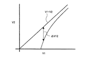
図50にV1とV2の関係を模式的に示す。図50からわかるように、液晶表示装置900では、V1の値が小さいほどΔV12の値が大きい。このように、V1の値が小さいほどΔV12の値が大きくなるので、とりわけ白浮特性を改善することができる。
FIG. 50 schematically shows the relationship between V1 and V2. As can be seen from FIG. 50, in the liquid
また、特許文献3に記載されているマルチ画素構造を高精細または大型の液晶テレビに適用する場合、振動電圧の振動の周期が表示パネルの高精細化あるいは大型化に伴って短くなるため、振動電圧発生のための回路の作製が困難になる(高価になる)、消費電力が増加する、あるいはCSバスラインの電気的な負荷インピーダンスによる波形鈍りの影響が大きくなるが、特許文献4に記載されているように、電気的に互いに独立な複数のCS幹線を設け、各CS幹線に複数のCSバスラインを接続することによって、CSバスラインを介して補助容量対向電極に印加する振動電圧の振動の周期を長くすることができる。 特許文献3および4の内容の全てを参考のために本明細書に援用する。
本出願人(譲受人)は、特許文献3および4に記載されているマルチ画素技術を適用した液晶表示装置を備えた大型の液晶テレビを市販している。これまでは、各画素を輝度が異なる2つの副画素(すなわち明副画素および暗副画素)で構成した2分割構造を採用していたが、表示面の大型化およびγ特性の視野角依存性のさらなる改善のためには、2分割では不十分であることがわかった。具体的には、表示装置の大型化に伴い1つの画素サイズが大きくなると、中間調を表示した際に、明副画素と暗副画素との市松状の配列が表示のざらつきとして視認されるという問題がある。
The present applicant (assignee) markets a large-sized liquid crystal television including a liquid crystal display device to which the multi-pixel technology described in
また、2分割構造においては、2つの副画素のV−Tカーブ(電圧−輝度(表示階調)曲線)を重ね合わせることによって、γ特性の視野角依存性を平均化するものであるため、斜め視野角におけるγ特性曲線が滑らかに変化せず、くびれが生じる。そのために、斜め視野角から表示画像を観察したときに、不自然に観察されるという問題がある。 In the two-divided structure, the viewing angle dependence of the γ characteristic is averaged by superimposing the VT curves (voltage-luminance (display gradation) curves) of two subpixels. The γ characteristic curve at an oblique viewing angle does not change smoothly, and constriction occurs. Therefore, there is a problem that when a display image is observed from an oblique viewing angle, it is unnaturally observed.
この問題を解決するためには、画素を3以上の副画素に分割する、すなわち、1つの画素のV−Tカーブを、3以上の互いに異なるV−Tカーブの重ね合わせで表現すればよい。特許文献3に記載されているマルチ画素技術において、画素分割数を増やすには、画素分割数の増加に応じて、電気的に互いに独立な補助容量対向電圧(CS信号電圧)の数を増加させればよい。
In order to solve this problem, the pixel may be divided into three or more sub-pixels, that is, the VT curve of one pixel may be expressed by superposing three or more different VT curves. In the multi-pixel technique described in
しかしながら、電気的に独立な補助容量対向電圧を用意するためには、CS幹線の数が増加するとともに、駆動回路が複雑になり、コストアップを招く。大型の液晶テレビをさらに普及させるためには、表示特性の改善もさることながら、価格を低下させることが重要であり、上記の方法は採用しがたい。 However, in order to prepare an electrically independent auxiliary capacitor counter voltage, the number of CS trunk lines increases, the drive circuit becomes complicated, and the cost increases. In order to further popularize large-sized liquid crystal televisions, it is important to lower the price as well as improving display characteristics, and the above method is difficult to adopt.
本発明は、上記諸点に鑑みてなされたものであり、その目的は、2分割構造を有する従来の液晶表示装置の駆動回路を複雑にすることなく、3分割以上の分割構造を実現することができる液晶表示装置を提供することにある。 The present invention has been made in view of the above points, and an object of the present invention is to realize a divided structure of three or more divisions without complicating a driving circuit of a conventional liquid crystal display device having a two-divided structure. An object of the present invention is to provide a liquid crystal display device that can be used.
本発明の液晶表示装置は、複数の行および複数の列を有するマトリクス状に配列された複数の画素と、前記複数の画素のそれぞれに関連付けられた、TFTと、ソースバスラインと、ゲートバスラインと、CSバスラインとを有し、前記複数の画素のそれぞれは、それぞれが互いに異なる電圧を保持し得る液晶容量を有する少なくとも3つの副画素を有し、前記ソースバスライン、ゲートバスライン、およびCSバスラインから、前記複数の画素のそれぞれに、少なくともある中間調において前記少なくとも3つの副画素の内の2つの副画素に互いに異なる輝度を表示させる信号を供給することによって、前記少なくとも3つの副画素に互いに異なる輝度を表示させることができる。 The liquid crystal display device of the present invention includes a plurality of pixels arranged in a matrix having a plurality of rows and a plurality of columns, a TFT, a source bus line, and a gate bus line associated with each of the plurality of pixels. Each of the plurality of pixels has at least three sub-pixels each having a liquid crystal capacitance capable of holding different voltages, and the source bus line, the gate bus line, and By supplying signals from the CS bus line to each of the plurality of pixels to display different luminances on two of the at least three subpixels in at least a certain halftone, the at least three subpixels. Different luminances can be displayed on the pixels.
ある実施形態において、前記複数の画素のそれぞれについて、前記少なくとも3つの副画素に対応する少なくとも3つのTFTと、1つのソースバスラインと、少なくとも1つのゲートバスラインと、少なくとも2つのCSバスラインが関連付けられており、前記少なくとも3つの副画素に対応するTFTのそれぞれは、ゲート電極、ソース電極およびドレイン電極を有している。 In one embodiment, for each of the plurality of pixels, at least three TFTs corresponding to the at least three subpixels, one source bus line, at least one gate bus line, and at least two CS bus lines are provided. Each of the TFTs associated with the at least three subpixels has a gate electrode, a source electrode, and a drain electrode.
ある実施形態において、前記少なくとも3つの副画素の有する液晶容量は、少なくとも3つの副画素電極と、液晶層と、前記液晶層を介して前記少なくとも3つの副画素電極に対向する対向電極とを有し、前記対向電極は前記少なくとも3つの副画素電極に共通の単一の電極である。 In one embodiment, the liquid crystal capacitance of the at least three subpixels includes at least three subpixel electrodes, a liquid crystal layer, and a counter electrode that faces the at least three subpixel electrodes through the liquid crystal layer. The counter electrode is a single electrode common to the at least three subpixel electrodes.
ある実施形態において、前記少なくとも3つの副画素を第1、第2および第3副画素とし、前記少なくとも2つのCSバスラインを第1および第2CSバスラインとすると、前記第1副画素は前記第1CSバスラインに接続された補助容量を有し、前記第2副画素は前記第2CSバスラインに接続された補助容量を有し、前記第3副画素は、前記第1CSバスラインに接続された補助容量と、前記第2CSバスラインに接続された補助容量とを有する。 In one embodiment, when the at least three subpixels are first, second, and third subpixels, and the at least two CS bus lines are first and second CS bus lines, the first subpixel is the first subpixel. An auxiliary capacitor connected to the 1CS bus line, the second sub-pixel has an auxiliary capacitor connected to the second CS bus line, and the third sub-pixel was connected to the first CS bus line An auxiliary capacitor and an auxiliary capacitor connected to the second CS bus line.
ある実施形態において、前記ゲートバスラインは、第1および第2ゲート配線を含み、前記第1CSバスラインは、第1および第2CS配線を含み、前記第2CSバスラインは、第3および第4CS配線を含む。 In one embodiment, the gate bus line includes first and second gate lines, the first CS bus line includes first and second CS lines, and the second CS bus line includes third and fourth CS lines. including.
ある実施形態において、前記第1および第2ゲート配線は前記液晶表示装置内において分岐されており、前記第1および第2CS配線は前記液晶表示装置内において分岐されており、前記第3および第4CS配線は前記液晶表示装置内において分岐されている。 In one embodiment, the first and second gate lines are branched in the liquid crystal display device, and the first and second CS lines are branched in the liquid crystal display device, and the third and fourth CSs are branched. The wiring is branched in the liquid crystal display device.
ある実施形態において、前記第1、第2および第3副画素は列方向に配列されており、前記第3副画素は、前記第1副画素と前記第2副画素との間に配置されている。 In one embodiment, the first, second, and third subpixels are arranged in a column direction, and the third subpixel is disposed between the first subpixel and the second subpixel. Yes.
ある実施形態において、前記第3副画素は、前記第1ゲート配線と接続するゲート電極を有するTFTと、前記第2ゲート配線と接続するゲート電極を有するTFTとを有している。 In one embodiment, the third subpixel includes a TFT having a gate electrode connected to the first gate wiring and a TFT having a gate electrode connected to the second gate wiring.
ある実施形態において、前記ゲートバスラインは、前記第1および第2ゲート配線を接続する接続配線をさらに有しており、前記CSバスラインは、前記第1および第2CS配線を接続する接続配線、および/または、前記第3および第4CS配線を接続する接続配線をさらに有しており、前記ゲートバスラインの前記接続配線は、前記ゲートバスラインの前記第1および第2ゲート配線と同じ材料から形成されており、前記CSバスラインの前記接続配線は、前記ソースバスラインと同じ材料から形成されている。 In one embodiment, the gate bus line further includes a connection wiring that connects the first and second gate wirings, and the CS bus line includes a connection wiring that connects the first and second CS wirings, And / or a connection wiring for connecting the third and fourth CS wirings, wherein the connection wiring of the gate bus line is made of the same material as the first and second gate wirings of the gate bus line. The connection wiring of the CS bus line is formed of the same material as that of the source bus line.
ある実施形態において、前記第3副画素が有する前記第1CSバスラインに接続された前記補助容量の静電容量値と、前記第2CSバスラインに接続された前記補助容量の静電容量値とが略等しい。 In one embodiment, the capacitance value of the auxiliary capacitance connected to the first CS bus line of the third subpixel and the capacitance value of the auxiliary capacitance connected to the second CS bus line are: Almost equal.
ある実施形態において、前記第1、第2および第3副画素が互いに異なる輝度を表示する場合、前記第3副画素の輝度は、前記第1、第2副画素の一方の輝度よりも高く、他方の輝度よりも低く、前記第3副画素は列方向にストライプ状に設けられている。 In one embodiment, when the first, second, and third subpixels display different luminances, the luminance of the third subpixel is higher than the luminance of one of the first, second subpixels, The third subpixel is provided in a stripe shape in the column direction, which is lower than the other luminance.
ある実施形態において、前記第1および第2副画素は列方向に配列されており、前記ソースバスラインは、前記第1および第2副画素と前記第3副画素との間に設けられている。 In one embodiment, the first and second subpixels are arranged in a column direction, and the source bus line is provided between the first and second subpixels and the third subpixel. .
ある実施形態において、前記第1、第2、第3副画素の面積比は1:1:1である。 In one embodiment, the area ratio of the first, second, and third subpixels is 1: 1: 1.
ある実施形態において、前記第3副画素は前記ゲートバスラインを跨いでいる。 In one embodiment, the third subpixel straddles the gate bus line.
ある実施形態において、前記第3副画素の副画素電極が前記ゲートバスラインを跨いでいる。 In one embodiment, the subpixel electrode of the third subpixel straddles the gate bus line.
ある実施形態において、前記第3副画素の副画素電極における前記ゲートバスラインを跨ぐ部分の行方向の長さは、前記第3副画素の副画素電極の行方向の最大の長さよりも短い。 In one embodiment, the length in the row direction of the portion of the subpixel electrode of the third subpixel across the gate bus line is shorter than the maximum length in the row direction of the subpixel electrode of the third subpixel.
ある実施形態において、前記第3副画素のTFTのドレイン電極は前記ゲートバスラインを跨いでいる。 In one embodiment, the drain electrode of the TFT of the third subpixel straddles the gate bus line.
ある実施形態において、前記第3副画素の副画素電極は、第1電極と、第2電極とを有しており、前記第3副画素のTFTのドレイン電極は前記ソースバスラインと平行に設けられており、前記ドレイン電極は、前記第3副画素の副画素電極の前記第1電極および前記第2電極を接続している。 In one embodiment, the subpixel electrode of the third subpixel includes a first electrode and a second electrode, and the drain electrode of the TFT of the third subpixel is provided in parallel with the source bus line. The drain electrode connects the first electrode and the second electrode of the subpixel electrode of the third subpixel.
ある実施形態において、前記第3副画素のTFTのドレイン電極が前記ゲートバスラインと重なる面積は、前記第1および第2副画素のTFTのドレイン電極が前記ゲートバスラインと重なるそれぞれの面積よりも小さい。 In one embodiment, the area where the drain electrode of the TFT of the third subpixel overlaps with the gate bus line is larger than the area where the drain electrode of the TFT of the first and second subpixel overlaps with the gate bus line. small.
ある実施形態において、前記第1および第2副画素は列方向に配列されており、前記第3副画素は、第1領域と、第2領域とを有しており、前記ソースバスラインは、前記第1および第2副画素と前記第3副画素の第1領域との間に設けられた第1ソース配線と、前記第1および第2副画素と前記第3副画素の第2領域との間に設けられた第2ソース配線とを有しており、前記第1および第2副画素の列方向のそれぞれの長さは、前記第3副画素の前記第1領域と前記第2領域の列方向のそれぞれの長さの半分であり、前記第1および第2副画素の行方向の長さは、前記第3副画素の前記第1領域または前記第2領域の行方向の長さの略4倍である。 In one embodiment, the first and second subpixels are arranged in a column direction, the third subpixel has a first region and a second region, and the source bus line is A first source line provided between the first and second subpixels and a first region of the third subpixel; a second region of the first and second subpixels and the third subpixel; Each of the first and second subpixels in the column direction has a length in the column direction of the first subpixel and the second region of the third subpixel. The length in the row direction of the first and second subpixels is the length in the row direction of the first region or the second region of the third subpixel. Is approximately four times as large as
ある実施形態において、前記第3副画素は、前記第1および第2領域に対応する副画素電極を有しており、前記第1、第2および第3副画素の副画素電極には、それぞれ、複数のTFTが接続されている。 In one embodiment, the third subpixel includes subpixel electrodes corresponding to the first and second regions, and the first, second, and third subpixels include subpixel electrodes, respectively. A plurality of TFTs are connected.
ある実施形態において、前記第1および第2ソース配線のそれぞれには複数のTFTが設けられており、前記第3副画素は、前記第1および第2領域に対応して設けられたTFTを有しており、前記第3副画素の前記第1および第2領域に設けられたTFTのドレイン電極のそれぞれの面積は、第1および第2副画素のTFTのドレイン電極のそれぞれの面積よりも小さい。 In one embodiment, each of the first and second source wirings is provided with a plurality of TFTs, and the third sub-pixel has TFTs provided corresponding to the first and second regions. The areas of the drain electrodes of the TFTs provided in the first and second regions of the third subpixel are smaller than the areas of the drain electrodes of the TFTs of the first and second subpixels. .
ある実施形態において、前記第1および第2副画素は、それぞれ、複数のTFTを有しており、前記第1および第2領域に設けられたTFTのそれぞれの数は、前記第1および第2副画素のTFTのそれぞれの数よりも少ない。 In one embodiment, the first and second subpixels each include a plurality of TFTs, and the number of TFTs provided in the first and second regions is the first and second TFTs, respectively. Less than the number of sub-pixel TFTs.
ある実施形態において、前記第1副画素は前記ある中間調において前記少なくとも3つの副画素の内で最高の輝度を呈し、前記第2および第3副画素の少なくとも一方は、前記第1副画素を挟むように配置された2つの領域を有する。 In one embodiment, the first subpixel exhibits the highest brightness among the at least three subpixels in the certain halftone, and at least one of the second and third subpixels includes the first subpixel. It has two areas arranged to be sandwiched.
ある実施形態において、前記第2および第3副画素の前記少なくとも一方は、前記2つの領域に亘って連続した副画素電極を有する。 In one embodiment, the at least one of the second and third subpixels has a subpixel electrode continuous over the two regions.
ある実施形態において、前記2つの領域に亘って連続した副画素電極は環状である。 In one embodiment, the subpixel electrode continuous over the two regions is annular.
ある実施形態において、前記2つの領域に亘って連続した副画素電極はコの字状である。 In one embodiment, the subpixel electrode continuous over the two regions has a U-shape.
ある実施形態において、前記第2および第3副画素の前記少なくとも一方は、前記2つの領域に対応する2つの副画素電極を有し、前記2つの副画素電極は、当該副画素に関連付けられたTFTのドレイン電極に接続されたドレイン引出し配線を介して互いに接続されている。 In one embodiment, the at least one of the second and third subpixels includes two subpixel electrodes corresponding to the two regions, and the two subpixel electrodes are associated with the subpixel. They are connected to each other through a drain lead wiring connected to the drain electrode of the TFT.
ある実施形態において、前記3つのTFTのドレイン電極にそれぞれ接続された3つのドレイン引出し配線を有し、前記第1および第2CSバスラインの少なくとも一方は延設部を有し、前記延設部は、絶縁層を介して前記少なくとも3つの副画素電極および前記3つのドレイン引出し配線の少なくとも1つと重なっている。 In one embodiment, there are three drain lead lines connected to the drain electrodes of the three TFTs, at least one of the first and second CS bus lines has an extension part, and the extension part has And at least one of the at least three sub-pixel electrodes and the three drain lead-out wirings through an insulating layer.
ある実施形態において、前記第1および第2CSバスラインの前記少なくとも一方が有する前記延設部は環状部を含む。 In one embodiment, the extending part included in the at least one of the first and second CS bus lines includes an annular part.
ある実施形態において、前記少なくとも3つの副画素電極の内の互いに隣接する副画素電極間の間隙には、前記ドレイン引出し配線、前記ソースバスライン、前記第1および第2CSバスラインの内から選択される少なくとも1つの配線の一部が配置されている。 In one embodiment, a gap between adjacent subpixel electrodes among the at least three subpixel electrodes is selected from the drain lead line, the source bus line, and the first and second CS bus lines. A part of at least one wiring is arranged.
ある実施形態において、垂直配向型の液晶層を有し、前記少なくとも3つの副画素電極の内の前記互いに隣接する副画素電極間の前記間隙は、列方向に対して約45°の方向に延びる間隙を含む。 In one embodiment, the liquid crystal layer has a vertically aligned liquid crystal layer, and the gap between the adjacent subpixel electrodes among the at least three subpixel electrodes extends in a direction of about 45 ° with respect to the column direction. Including gaps.
ある実施形態において、前記第1、第2および第3副画素は、前記第1および第2CSバスラインの間に配置され、前記第1および第2CSバスラインは、それぞれ、列方向に隣接する画素の補助容量に接続している。 In one embodiment, the first, second, and third sub-pixels are disposed between the first and second CS bus lines, and the first and second CS bus lines are pixels adjacent in the column direction, respectively. Connected to the auxiliary capacity.
ある実施形態において、前記第1、第2および第3副画素の副画素電極のそれぞれにおける列方向に沿った2つの辺の長さは略等しい。 In one embodiment, the lengths of two sides along the column direction in each of the subpixel electrodes of the first, second, and third subpixels are substantially equal.
ある実施形態において、前記少なくとも1つのゲートバスラインは第1および第2ゲート配線を有しており、前記第3副画素は、前記第1ゲート配線と接続されたゲート電極を有するTFTと、前記第2ゲート配線と接続されたゲート電極を有するTFTとを有しており、前記第3副画素の2つのTFTのドレイン電極は、2つのドレイン引出し配線とそれぞれ接続されており、前記2つのドレイン引出し配線は、前記少なくとも1つのゲートバスラインとそれぞれ交差する。 In one embodiment, the at least one gate bus line includes first and second gate lines, and the third subpixel includes a TFT having a gate electrode connected to the first gate line, and A TFT having a gate electrode connected to the second gate wiring, and the drain electrodes of the two TFTs of the third subpixel are connected to two drain lead wirings, respectively, and the two drains The lead wiring intersects with the at least one gate bus line.
ある実施形態において、前記少なくとも1つのゲートバスラインはゲート配線を有しており、前記第3副画素は、それぞれが前記ゲート配線と接続されたゲート電極を有する2つのTFTを有しており、前記第3副画素の2つのTFTのドレイン電極は、2つのドレイン引出し配線とそれぞれ接続されており、前記第3副画素の副画素電極は前記ゲートバスラインを跨ぐ。 In one embodiment, the at least one gate bus line has a gate wiring, and the third sub-pixel has two TFTs each having a gate electrode connected to the gate wiring, The drain electrodes of the two TFTs of the third subpixel are connected to two drain lead lines, respectively, and the subpixel electrode of the third subpixel straddles the gate bus line.
ある実施形態において、前記第3副画素の副画素電極は、第1電極と、第2電極と、前記第1および第2電極を連結する連結部とを有しており、前記連結部の行方向の長さは、前記第1、第2電極の前記行方向の長さよりも短い。 In one embodiment, the subpixel electrode of the third subpixel includes a first electrode, a second electrode, and a connecting portion that connects the first and second electrodes, and the row of the connecting portions. The length in the direction is shorter than the length in the row direction of the first and second electrodes.
ある実施形態において、前記第3副画素の副画素電極の連結部は、前記画素の行方向における中央付近に設けられている。 In one embodiment, the connecting portion of the subpixel electrodes of the third subpixel is provided near the center in the row direction of the pixel.
ある実施形態において、前記第1副画素のTFTおよび前記第3副画素の一方のTFTのゲート電極、ならびに/または、前記第2副画素のTFTおよび前記第3副画素の他方のTFTのゲート電極は、ゲート電極部として一体的に設けられて前記ゲートバスラインに接続されており、前記第1および第2副画素のTFTのそれぞれのドレイン電極は前記ゲート電極部および前記ゲートバスラインと重なる。 In one embodiment, the gate electrode of one TFT of the first subpixel and the third subpixel and / or the gate electrode of the other TFT of the second subpixel and the other TFT of the third subpixel. Are integrally provided as a gate electrode portion and connected to the gate bus line, and the drain electrodes of the TFTs of the first and second subpixels overlap the gate electrode portion and the gate bus line, respectively.
ある実施形態において、前記2つのドレイン引出し配線は、前記第1および第2CSバスラインとそれぞれ重なり、前記第1および第2副画素の副画素電極は、前記2つのドレイン引出し配線と前記第1および第2CSバスラインとが重なる領域とは重ならない。 In one embodiment, the two drain lead lines overlap with the first and second CS bus lines, respectively, and the sub-pixel electrodes of the first and second sub-pixels are the two drain lead lines and the first and second sub-line electrodes, respectively. It does not overlap with the area where the second CS bus line overlaps.
ある実施形態において、前記第3副画素の副画素電極は、前記2つのドレイン引出し配線とコンタクトホールをそれぞれ介して接続されており、前記2つのドレイン引出し配線は前記第1および第2CSバスラインと重なる補助容量電極をそれぞれ有している。 In one embodiment, the sub-pixel electrode of the third sub-pixel is connected to the two drain lead wirings through contact holes, respectively, and the two drain lead wirings are connected to the first and second CS bus lines. Each has an overlapping auxiliary capacitance electrode.
ある実施形態において、前記少なくとも1つのゲートバスラインは第1および第2ゲート配線を有しており、前記第3副画素は、前記第1ゲート配線または前記第2ゲート配線に接続されたゲート電極を有するTFTを有している。 In one embodiment, the at least one gate bus line includes first and second gate lines, and the third subpixel includes a gate electrode connected to the first gate line or the second gate line. A TFT having
ある実施形態において、前記第3副画素のTFTのドレイン電極は、ドレイン引出し配線に接続されており、前記ドレイン引出し配線は、前記第1および第2CSバスラインと重なり、前記第1および第2副画素の副画素電極は、前記ドレイン引出し配線と前記第1および第2CSバスラインとが重なる領域とは重ならない。 In one embodiment, the drain electrode of the TFT of the third sub-pixel is connected to a drain lead wiring, and the drain lead wiring overlaps with the first and second CS bus lines, and the first and second sub-wiring lines overlap. The sub-pixel electrode of the pixel does not overlap with the region where the drain lead-out wiring and the first and second CS bus lines overlap.
ある実施形態において、行方向に沿った画素において、少なくとも1つの画素ごとに前記第3副画素のTFTのゲート電極が異なるゲート配線に接続している。 In one embodiment, in the pixels along the row direction, the gate electrodes of the TFTs of the third subpixel are connected to different gate wirings for each at least one pixel.
ある実施形態において、行方向に隣接する2つの画素のうち、一方の画素の第3副画素のTFTのゲート電極は前記第1ゲート配線に接続しており、他方の画素の第3副画素のTFTのゲート電極は前記第2ゲート配線に接続している。 In one embodiment, the gate electrode of the TFT of the third subpixel of one of the two pixels adjacent in the row direction is connected to the first gate wiring, and the third subpixel of the other pixel is connected. The gate electrode of the TFT is connected to the second gate wiring.
ある実施形態において、前記第3副画素のTFTのドレイン電極の面積は、前記第1および第2副画素のTFTのドレイン電極のそれぞれの面積よりも小さい。 In one embodiment, the area of the drain electrode of the TFT of the third subpixel is smaller than the area of the drain electrode of the TFT of the first and second subpixels.
ある実施形態において、前記第1、第2および第3副画素の面積は互いにほぼ等しい。 In one embodiment, the areas of the first, second and third subpixels are substantially equal to each other.
ある実施形態において、前記複数の画素のそれぞれは、第4副画素をさらに有しており、前記第4副画素は、前記第1CSバスラインに接続された補助容量と、前記第2CSバスラインに接続された補助容量とを有する。 In one embodiment, each of the plurality of pixels further includes a fourth sub-pixel, and the fourth sub-pixel includes an auxiliary capacitor connected to the first CS bus line and the second CS bus line. Connected auxiliary capacity.
ある実施形態において、前記第3副画素において、前記第1CSバスラインに接続された補助容量を第1補助容量とし、前記第2CSバスラインに接続された補助容量を第2補助容量とし、前記第4副画素において、前記第1CSバスラインに接続された補助容量を第3補助容量とし、前記第2CSバスラインに接続された補助容量を第4補助容量とすると、前記第1補助容量の静電容量値と前記第2補助容量の静電容量値とが異なり、前記第3補助容量の静電容量値と前記第4補助容量の静電容量値とが異なる。 In one embodiment, in the third sub-pixel, the auxiliary capacitor connected to the first CS bus line is a first auxiliary capacitor, the auxiliary capacitor connected to the second CS bus line is a second auxiliary capacitor, and In the four sub-pixels, assuming that the auxiliary capacitor connected to the first CS bus line is a third auxiliary capacitor and the auxiliary capacitor connected to the second CS bus line is a fourth auxiliary capacitor, the electrostatic capacity of the first auxiliary capacitor is The capacitance value is different from the capacitance value of the second auxiliary capacitance, and the capacitance value of the third auxiliary capacitance is different from the capacitance value of the fourth auxiliary capacitance.
ある実施形態において、前記ソースバスラインは、第1および第2ソース配線を有しており、前記第1および第2副画素は、前記第1ソース配線と前記第2ソース配線との間において列方向に配列されており、前記第1および第2副画素に対して、前記第1ソース配線を挟んで前記第3副画素が配置され、前記第2ソース配線を挟んで前記第4副画素が配置されている。 In one embodiment, the source bus line includes first and second source lines, and the first and second subpixels are arranged between the first source line and the second source line. The third subpixels are arranged with respect to the first and second subpixels with the first source wiring interposed therebetween, and the fourth subpixels with the second source wiring interposed therebetween. Has been placed.
ある実施形態において、前記第3および第4副画素は前記ゲートバスラインを跨いでいる。 In one embodiment, the third and fourth subpixels straddle the gate bus line.
ある実施形態において、前記第1、第2、第3および第4副画素は、それぞれ、複数のTFTを有している。 In one embodiment, each of the first, second, third, and fourth subpixels includes a plurality of TFTs.
ある実施形態において、前記第3および第4副画素の副画素電極が前記ゲートバスラインを跨いでいる。 In one embodiment, subpixel electrodes of the third and fourth subpixels straddle the gate bus line.
ある実施形態において、前記第3および第4副画素の副画素電極において前記ゲートバスラインを跨いでいる部分の行方向の長さは、前記第3、第4副画素の副画素電極の行方向の最大の長さよりも短い。 In one embodiment, the length in the row direction of the portion of the subpixel electrode of the third and fourth subpixels that straddles the gate bus line is the row direction of the subpixel electrode of the third and fourth subpixels. Shorter than the maximum length of.
ある実施形態において、前記第3および第4副画素のTFTのドレイン電極は前記ゲートバスラインを跨いでいる。 In one embodiment, the drain electrodes of the TFTs of the third and fourth subpixels straddle the gate bus line.
ある実施形態において、前記第3および第4副画素の副画素電極は、それぞれ、2つの電極を有しており、前記第3および第4副画素のTFTのドレイン電極は前記ソースバスラインと平行して設けられており、前記第3および第4副画素のTFTのドレイン電極は、前記第3および第4副画素の副画素電極の前記2つの電極をそれぞれ接続している。 In one embodiment, the subpixel electrodes of the third and fourth subpixels each have two electrodes, and the drain electrodes of the TFTs of the third and fourth subpixels are parallel to the source bus line. The drain electrodes of the TFTs of the third and fourth subpixels are connected to the two electrodes of the subpixel electrodes of the third and fourth subpixels, respectively.
ある実施形態において、前記第1、第2、第3および第4副画素のTFTのドレイン電極は前記ゲートバスラインと重なり、前記第3および第4副画素のTFTのドレイン電極が前記ゲートバスラインと重なるそれぞれの面積は、前記第1および第2副画素のTFTのドレイン電極が前記ゲートバスラインと重なるそれぞれの面積よりも小さい。 In one embodiment, the drain electrodes of the TFTs of the first, second, third, and fourth subpixels overlap the gate bus line, and the drain electrodes of the TFTs of the third and fourth subpixels are the gate bus line. The areas of the first and second subpixel TFTs overlapping each other are smaller than the respective areas overlapping the gate bus lines.
ある実施形態において、前記第1および第2副画素は、それぞれ、複数のTFTを有しており、前記第3および第4副画素のそれぞれのTFTの数は、前記第1、第2副画素のそれぞれのTFTの数よりも少ない。 In one embodiment, each of the first and second subpixels includes a plurality of TFTs, and each of the third and fourth subpixels includes the first and second subpixels. Less than the number of each TFT.
ある実施形態において、前記第1、第2、第3および第4副画素の面積は互いにほぼ等しい。 In one embodiment, the areas of the first, second, third and fourth subpixels are substantially equal to each other.
ある実施形態において、前記少なくとも3つの副画素を第1、第2および第3副画素とし、前記少なくとも2つのCSバスラインを第1および第2CSバスラインとすると、前記第1副画素は前記第1CSバスラインに接続された補助容量を有し、前記第2副画素は前記第2CSバスラインに接続された補助容量を有し、前記第3副画素は前記少なくとも1つのゲートバスラインに接続された補助容量を有する。 In one embodiment, when the at least three subpixels are first, second, and third subpixels, and the at least two CS bus lines are first and second CS bus lines, the first subpixel is the first subpixel. An auxiliary capacitor connected to the 1CS bus line, the second sub-pixel has an auxiliary capacitor connected to the second CS bus line, and the third sub-pixel is connected to the at least one gate bus line. Have auxiliary capacity.
ある実施形態において、前記第1、第2および第3副画素は、隣接する2つのゲートバスラインの間に設けられ、前記第1、第2および第3副画素のTFTのゲート電極は、前記2つのゲートバスラインのうちの一方のゲートバスラインと接続されており、前記第1および第2CSバスラインは、前記2つのゲートバスラインの間に設けられ、前記第3副画素の補助容量は、前記2つのゲートバスラインのうちの他方のゲートバスラインと接続されている。 In one embodiment, the first, second and third subpixels are provided between two adjacent gate bus lines, and the gate electrodes of the TFTs of the first, second and third subpixels are It is connected to one of the two gate bus lines, the first and second CS bus lines are provided between the two gate bus lines, and the auxiliary capacitance of the third subpixel is Are connected to the other of the two gate bus lines.
ある実施形態において、前記第1、第2および第3副画素は、前記第1および第2CSバスラインの間に配置され、前記第3副画素の補助容量は、列方向に隣接する画素を選択するためのゲートバスラインと接続されている。 In one embodiment, the first, second, and third subpixels are disposed between the first and second CS bus lines, and the auxiliary capacitance of the third subpixel selects pixels adjacent in the column direction. Connected to the gate bus line.
ある実施形態において、前記複数の画素は、赤を表示する赤画素と、青を表示する青画素と、緑を表示する緑画素とを有しており、前記青画素のセルギャップが前記赤画素または前記緑画素よりも小さい。 In one embodiment, the plurality of pixels include a red pixel that displays red, a blue pixel that displays blue, and a green pixel that displays green, and a cell gap of the blue pixel is the red pixel. Or smaller than the green pixel.
本発明による液晶表示装置は、駆動回路を複雑にすることなく、3分割構造を実現できるので、コストの上昇を抑制しつつ、表示品位(特に、γ特性の視野角依存性)を改善することができる。 Since the liquid crystal display device according to the present invention can realize a three-part structure without complicating the drive circuit, the display quality (particularly, the viewing angle dependency of the γ characteristic) can be improved while suppressing an increase in cost. Can do.
10 画素
10a、10b 副画素
12 走査線(ゲートバスライン)
14 信号線(ソースバスライン)
16a、16b TFT
18a、18b 副画素電極
100、100A、100B、100C、100D、200A、200B、200C、200C’、200D、300B、300C、300D、300E、300F、400A、400B、500A、500B、500C、500D、600A、600B、600C、600C1、600C2、600C3、600C4 液晶表示装置
111a、111b、111c 副画素電極
112 ゲートバスライン(Gバスライン)
113 CSバスライン
114 ソースバスライン(Sバスライン)
116a、116b、116c TFT
117a、117b、117c、117c1、117c2、117d1、117d2 ドレイン引出し配線
118a、118b、118c1、118c2、118d1、118d2 補助容量電極
119a、119b、119c コンタクト部
SP−A、SP−B、SP−C、SP−D 副画素
TFT−A、TFT−A1、TFT−A2、TFT−B、TFT−B1、TFT−B2、TFT−C、TFT−C1、TFT−C2、TFT−D、TFT−D1、TFT−D2 薄膜トランジスタ
CCS−A、CCS−B、CCS−C、CCS−C1、CCS−C2、CCS−D、CCS−D1、CCS−D2 補助容量
CLC−A、CLC−B、CLC−C、CLC−D 液晶容量10
14 Signal line (source bus line)
16a, 16b TFT
18a,
113
116a, 116b, 116c TFT
117a, 117b, 117c, 117c1, 117c2, 117d1, 117d2
以下、図面を参照して本発明による実施形態の液晶表示装置およびそれに用いられるTFT基板の構成を説明する。なお、本発明は以下の実施形態に限定されるものではない。 The configuration of a liquid crystal display device according to an embodiment of the present invention and a TFT substrate used therefor will be described below with reference to the drawings. In addition, this invention is not limited to the following embodiment.
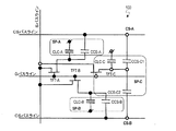
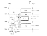
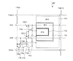
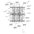
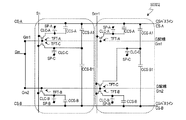
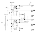
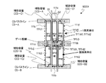
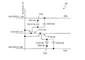
図1は、本発明による実施形態の液晶表示装置100の1画素分の等価回路を模式的に示す図である。液晶表示装置100の各画素は、3つの副画素SP−A、SP−BおよびSP−Cを有し、それぞれが3つの副画素SP−A、SP−BおよびSP−Cに対応する3つのTFT−A、TFT−BおよびTFT−Cと、1つのソースバスライン(Sバスライン)と、1つのゲートバスライン(Gバスライン)と、2つのCSバスラインCS−AおよびCS−Bが各画素に関連付けられている。
FIG. 1 is a diagram schematically showing an equivalent circuit for one pixel of a liquid
図48に示した従来の液晶表示装置900の等価回路と比較すると明らかなように、液晶表示装置100は、1つの画素が3つの副画素SP−A、SP−BおよびSP−Cを有している一方、液晶表示装置100の画素に対応する部分以外の構成、すなわち、Gバスライン、SバスラインおよびCSバスラインの数は液晶表示装置900と同じであり、これらに対応する信号(電圧)を供給する駆動回路(不図示)の構成も液晶表示装置900と同じである。このように、液晶表示装置100は、従来の2分割構造を有する液晶表示装置900の駆動回路を複雑にすることなく、3分割構造を実現している。従って、本発明の実施形態によると、コストの上昇を抑制しつつ、表示品位(特に、γ特性の視野角依存性)を改善することができる。
As apparent from comparison with the equivalent circuit of the conventional liquid
液晶表示装置100における、2つの副画素SP−AおよびSP−Bと、TFT−AおよびTFT−B、Gバスライン、Sバスライン、および2本の互いに電気的に独立なCSバスラインとの間の接続関係は、液晶表示装置900と全く同じである(簡単のために説明を省略)。液晶表示装置900に対して付加された3番目の副画素SP−Cは以下のように接続されている。
In the liquid
副画素SP−Cは、液晶容量CLC−Cと、2つの補助容量CCS−C1およびCCS−C2とを有している。液晶容量CLC−Cの一方の電極(副画素電極)はTFT−Cのドレイン電極に接続されており、補助容量CCS−C1およびCCS−C2のそれぞれの一方の電極(補助容量電極)もTFT−Cのドレイン電極に接続されている。TFT−Cは、他のTFT−AおよびTFT−Bと同様に、ゲート電極は共通のGバスラインに接続されており、ソース電極はSバスラインに接続されている。液晶容量CLC−Cの他方の電極(対向電極)は、他の液晶容量CLC−AおよびCLC−Bと共通の対向電極で構成されている。補助容量CCS−C1の他方の電極(補助容量対向電極)は、CSバスラインCS−Aに接続されており、補助容量CCS−C2の他方の電極(補助容量対向電極)は、CSバスラインCS−Bに接続されている。従って、液晶容量CLC−Cに印加される電圧は、2つの補助容量CCS−C1およびCCS−C2を介して、CSバスラインCS−Aによる突き上げ(または突き下げ)とCSバスラインCS−Bによる突き下げ(または突き上げ)との両方の作用を受け、液晶容量CLC−Aに印加される実効電圧と液晶容量CLC−Bに印加される実効電圧との中間の値となる。 The sub-pixel SP-C has a liquid crystal capacitor CLC-C and two auxiliary capacitors CCS-C1 and CCS-C2. One electrode (subpixel electrode) of the liquid crystal capacitor CLC-C is connected to the drain electrode of the TFT-C, and one electrode (auxiliary capacitor electrode) of each of the auxiliary capacitors CCS-C1 and CCS-C2 is also TFT- It is connected to the C drain electrode. As in the other TFT-A and TFT-B, the TFT-C has a gate electrode connected to a common G bus line and a source electrode connected to an S bus line. The other electrode (counter electrode) of the liquid crystal capacitor CLC-C is composed of a common electrode common to the other liquid crystal capacitors CLC-A and CLC-B. The other electrode (auxiliary capacitor counter electrode) of the auxiliary capacitor CCS-C1 is connected to the CS bus line CS-A, and the other electrode (auxiliary capacitor counter electrode) of the auxiliary capacitor CCS-C2 is connected to the CS bus line CS. Connected to -B. Therefore, the voltage applied to the liquid crystal capacitor CLC-C is pushed up (or pushed down) by the CS bus line CS-A and the CS bus line CS-B via the two auxiliary capacitors CCS-C1 and CCS-C2. Under the action of both push-down (or push-up), the value becomes an intermediate value between the effective voltage applied to the liquid crystal capacitor CLC-A and the effective voltage applied to the liquid crystal capacitor CLC-B.
なお、ここでは1つのGバスラインが3つのTFTについて共通に接続されているが、これに限ることはなく、各TFTに1つのGバスラインを設けるなど、各画素に関連付けられるGバスラインは複数であってもよい。 Here, one G bus line is commonly connected to three TFTs. However, the present invention is not limited to this. For example, one G bus line is provided for each TFT. There may be a plurality.
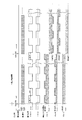
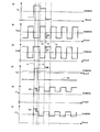
図2は、液晶表示装置100の駆動方法を説明するための図であり、ゲート信号(Gate信号)、CS信号(補助容量対向電圧)、Sバスラインから供給される信号電圧(=ソース信号、S信号)および画素電圧(各副画素の液晶容量に印加される電圧=各副画素の副画素電極の電圧)の波形を示す図である。また、図中の破線は対向電極の電圧波形COMMON(Vcom)を示している。あるゲートバスライン(ここではGate:001)において、ゲート信号がローからハイに切り替わったときに信号電圧がそれぞれの副画素に書き込まれる。それぞれの副画素に書き込まれた信号電圧が、上述の通り、それぞれ突き上げの作用、突き下げの作用、および突き上げと突き下げの両方の作用を受け、各副画素電極の電圧が、VClc−A、VClc−B、VClc−Cに示す波形となる。なお、ここでは簡便のため、各TFTの寄生容量等の影響による引き込み電圧は無視している。画素の印加電圧の波形を示す図中の一点鎖線は副画素電極の実効電圧を示している。VClc−Cは波形に変動がないため、実効電圧はVClc−Cの波形と同一となる。
FIG. 2 is a diagram for explaining a driving method of the liquid
一垂直走査期間(ここでは入力映像信号のフレームと同じ)に信号電圧の極性が反転し、且つ、行方向および列方向に隣接する画素間の極性が逆となる、典型的なドット反転駆動の場合を例示する。注目する画素において、nフレーム(nF)では正極性書き込み、n+1フレーム(n+1 F)では負極性書き込みの場合を示す。ここでは特に示さない限り、「一垂直走査期間」とは、入力映像信号で規定される期間ではなく、液晶表示装置について規定される期間であり、ある画素に信号電圧が供給されてから、再び信号電圧が供給されるまでの期間である。例えば、NTSC信号の1フレームは33.3msであるが、一般に液晶表示装置ではNTSC信号の1/2フレーム=1フィールド(16.7ms)の期間内に全ての画素に信号電圧の書き込みを行っており、16.7msが液晶表示装置の一垂直走査期間である。さらに、応答特性を改善する目的などのために倍速駆動を行う場合、液晶表示装置の一垂直走査期間は、さらに半分の8.3msとなる。また、各画素に供給される「信号電圧」とは、表示すべき階調に対応する電圧(階調電圧)に限られず、応答特性を改善するためのオーバーシュート電圧や、擬似インパルス駆動(黒挿入駆動)のための黒表示電圧など、画素に供給される全ての電圧を含むものとする。 A typical dot inversion driving method in which the polarity of the signal voltage is inverted in one vertical scanning period (here, the same as the frame of the input video signal) and the polarity between adjacent pixels in the row direction and the column direction is inverted. The case is illustrated. In the pixel of interest, the case of positive polarity writing in n frame (nF) and the case of negative polarity writing in n + 1 frame (n + 1 F) is shown. Here, unless otherwise indicated, the “one vertical scanning period” is not a period defined by the input video signal but a period defined for the liquid crystal display device, and again after a signal voltage is supplied to a certain pixel. This is the period until the signal voltage is supplied. For example, one frame of an NTSC signal is 33.3 ms. In general, in a liquid crystal display device, a signal voltage is written to all pixels within a period of 1/2 frame of NTSC signal = 1 field (16.7 ms). 16.7 ms is one vertical scanning period of the liquid crystal display device. Further, when double speed driving is performed for the purpose of improving response characteristics, the vertical scanning period of the liquid crystal display device is halved to 8.3 ms. In addition, the “signal voltage” supplied to each pixel is not limited to a voltage (grayscale voltage) corresponding to a grayscale to be displayed, but an overshoot voltage for improving response characteristics or pseudo impulse drive (black voltage). It is assumed that all voltages supplied to the pixel, such as a black display voltage for insertion driving), are included.
nフレームでは正極性書き込みなので、ゲート信号が立ち下がった直後のCS信号の振幅が増大するVCS−Aが供給される液晶容量CLC−Aに印加される実効電圧が、CS電圧による突き上げ作用を受けて増大し、液晶容量CLC−Aで構成される副画素SP−Aが明副画素となる。一方、ゲート信号が立ち下がった直後のCS信号の振幅が減少するVCS−Bが供給される液晶容量CLC−Bに印加される実効電圧はCS電圧による突き下げ作用を受けて減少し、液晶容量CLC−Bで構成される副画素SP−Bが暗副画素となる。 Since the n-frame is positive writing, the effective voltage applied to the liquid crystal capacitor CLC-A supplied with VCS-A in which the amplitude of the CS signal increases immediately after the gate signal falls is subjected to the pushing action by the CS voltage. The sub-pixel SP-A composed of the liquid crystal capacitor CLC-A becomes a bright sub-pixel. On the other hand, the effective voltage applied to the liquid crystal capacitor CLC-B supplied with VCS-B in which the amplitude of the CS signal decreases immediately after the gate signal falls decreases due to the push-down action by the CS voltage, and the liquid crystal capacitor The sub-pixel SP-B configured by CLC-B is a dark sub-pixel.
液晶容量CLCに印加される実効電圧は、VCS−Aの突き上げ作用およびVCS−Bの突き下げ作用の両方を受けるので、液晶容量CLC−Aに印加される実効電圧と液晶容量CLC−Bに印加される実効電圧との中間の値となり、液晶容量CLC−Cで構成される副画素SP−Cは中間の輝度を呈する副画素(中副画素ということがある。)となる。ここでは、副画素SP−Cが有する2つの補助容量CCS−C1およびCCS−C2の静電容量値が互いに等しい場合を例示しており、この場合には、VCS−AおよびVCS−Bの作用が互いに相殺し合い、液晶容量CLC−Cには信号電圧と等しい電圧が印加されることになる。なお、このように液晶容量CLC−Cには信号電圧と等しい電圧を印加する場合には、副画素SP−Cの補助容量を1つだけにし、且つ、当該補助容量をオンゲート構造、すわなち、GバスラインをCSバスラインの代わりに用いる構造とすれば、駆動回路を複雑にすることなく同様の効果を得ることができる。 Since the effective voltage applied to the liquid crystal capacitor CLC is subjected to both the push-up action of VCS-A and the push-down action of VCS-B, the effective voltage applied to the liquid crystal capacity CLC-A and the liquid crystal capacity CLC-B are applied. The sub-pixel SP-C composed of the liquid crystal capacitance CLC-C becomes a sub-pixel (which may be called a middle sub-pixel) exhibiting intermediate luminance. Here, the case where the capacitance values of the two auxiliary capacitors CCS-C1 and CCS-C2 included in the sub-pixel SP-C are equal to each other is illustrated. In this case, the operations of the VCS-A and the VCS-B are illustrated. Cancel each other, and a voltage equal to the signal voltage is applied to the liquid crystal capacitor CLC-C. When a voltage equal to the signal voltage is applied to the liquid crystal capacitor CLC-C in this way, only one auxiliary capacitor of the sub-pixel SP-C is used, and the auxiliary capacitor has an on-gate structure, that is, If the G bus line is used in place of the CS bus line, the same effect can be obtained without complicating the drive circuit.
本実施形態はこれに限られず、補助容量CCS−C1およびCCS−C2の値を適宜設定することによって、副画素SP−Cの呈する輝度を副画素SP−Aの輝度に近づけることも、副画素SP−Bの輝度に近づけることもできる。なお、γ特性の視野角依存性の観点からは、後述するように、副画素SP−Cの輝度を副画素SP−Aの輝度と副画素SP−Bの輝度との中間とし、且つ、副画素SP−A、BおよびCの面積を互いに等しくすることが好ましい(図17参照)。ここで、副画素SP−Cの呈する輝度を明副画素の輝度に近づけると、コントラスト比を向上させることができ、副画素SP−Cの呈する輝度を暗副画素の輝度に近づけると、特に低階調におけるγ特性の視野角依存性を改善することができる。 The present embodiment is not limited to this, and by appropriately setting the values of the auxiliary capacitors CCS-C1 and CCS-C2, the luminance exhibited by the subpixel SP-C can be brought close to the luminance of the subpixel SP-A. It can also be close to the brightness of SP-B. From the viewpoint of the viewing angle dependency of the γ characteristic, the luminance of the subpixel SP-C is set between the luminance of the subpixel SP-A and the luminance of the subpixel SP-B, as described later, and It is preferable to make the areas of the pixels SP-A, B, and C equal to each other (see FIG. 17). Here, the contrast ratio can be improved by bringing the luminance exhibited by the subpixel SP-C closer to the luminance of the bright subpixel, and particularly when the luminance presented by the subpixel SP-C is brought closer to the luminance of the dark subpixel. The viewing angle dependence of the γ characteristic in gradation can be improved.
また、上述の説明から明らかなように、2つの補助容量を有する副画素SP−Cを2つ設け、2つの副画素SP−Cが有する2つの補助容量の静電容量値を適宜設定すれば、互いに異なる4つの輝度を呈する4つの副画素を形成することができる。例えば、図1において、副画素SP−Cと電気的に等価な副画素をSP−Dを追加する。SP−Dは、SP−Cと同様に、液晶容量CLC−Dと2つの補助容量CCS−D1およびCCS−D2を有する。ここで、副画素SP−Cにおいては、補助容量CCS−C1およびCCS−C2の静電容量値を調整し突き上げ作用(または突き下げ作用)を優勢とし、副画素SP−Dにおいては補助容量CCS−D1およびCCS−D2の静電容量値を調整し突き下げ作用(または突き上げ作用)を優勢とすることによって、4つの異なる輝度を呈する副画素を得ることができる。このように、4つの異なる輝度を呈する副画素を設ければ、γ特性の視野角依存性をさらに改善することができる。以下では、本発明の最も基本的な実施形態である、3分割構造を有する液晶表示装置を説明する。 Further, as is clear from the above description, if two subpixels SP-C having two auxiliary capacitors are provided and the capacitance values of the two auxiliary capacitors included in the two subpixels SP-C are appropriately set. , Four sub-pixels exhibiting four different luminances can be formed. For example, in FIG. 1, SP-D is added as a subpixel electrically equivalent to the subpixel SP-C. Similar to SP-C, SP-D has a liquid crystal capacitor CLC-D and two auxiliary capacitors CCS-D1 and CCS-D2. Here, in the sub-pixel SP-C, the capacitance values of the auxiliary capacitors CCS-C1 and CCS-C2 are adjusted to make the push-up action (or push-down action) dominant, and in the sub-pixel SP-D, the auxiliary capacity CCS. By adjusting the capacitance values of -D1 and CCS-D2 to make the push-down action (or push-up action) dominant, subpixels exhibiting four different luminances can be obtained. Thus, if the sub-pixel which exhibits four different brightness | luminances is provided, the viewing angle dependence of (gamma) characteristic can further be improved. Hereinafter, a liquid crystal display device having a three-part structure, which is the most basic embodiment of the present invention, will be described.
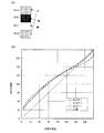
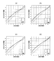
図3は、MVA型の液晶表示装置のγ特性を示すグラフであり、画素分割無し(曲線L0)、2分割構造(曲線L2)、3分割構造(L=3)のそれぞれの右60°視野角におけるγ曲線と、理想的なγ曲線(L1)を示している。MVA型液晶表示装置の斜め視野角におけるγ曲線が高輝度側にずれるという問題が、画素分割駆動によって改善されることがわかる。また、3分割構造のγ曲線L3の方が2分割構造のγ曲線L2よりも、理想的なγ曲線に近く、視野角特性が優れている。さらに、2分割構造のγ曲線L2は100/255階調付近の変化が滑らかでないのに対し、3分割構造のγ曲線L3は全階調範囲に亘って滑らかに変化していることがわかる。 FIG. 3 is a graph showing the γ characteristics of the MVA type liquid crystal display device, each having a 60 ° right field of view with no pixel division (curve L0), two division structure (curve L2), and three division structure (L = 3). A γ curve at the corner and an ideal γ curve (L1) are shown. It can be seen that the problem that the γ curve at the oblique viewing angle of the MVA type liquid crystal display device shifts to the high luminance side is improved by pixel division driving. Further, the γ curve L3 having a three-part structure is closer to an ideal γ curve than the γ curve L2 having a two-part structure, and the viewing angle characteristics are superior. Further, it can be seen that the γ curve L2 of the two-divided structure does not change smoothly around the 100/255 gradation, whereas the γ curve L3 of the three-divided structure changes smoothly over the entire gradation range.
なお、全ての階調電圧について、液晶容量に印加される実効電圧を異ならせる必要は必ずしもなく、最低階調(黒表示状態)および最高階調(白表示状態)においては、各液晶容量に同じ電圧が印加され、同じ輝度(階調)を表示してもよい。また、特にγ特性の視野角依存性が大きい領域(ある中間調(例えば100/255階調)よりも低い領域)においてのみ、マルチ画素駆動を行っても良い。 Note that it is not always necessary to vary the effective voltage applied to the liquid crystal capacitance for all gradation voltages, and the same for each liquid crystal capacitance at the lowest gradation (black display state) and the highest gradation (white display state). A voltage may be applied to display the same luminance (gradation). In addition, multi-pixel driving may be performed only in a region where the gamma characteristic has a large viewing angle dependency (a region lower than a certain halftone (for example, 100/255 gradation)).
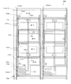
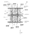
次に、図4〜図7を参照して、本発明による実施形態の液晶表示装置の画素分割構造と副画素の配置を説明する。図4〜図7は1画素構造分の等価回路と副画素の配置を模式的に示す図である。尚、副画素の配置は例示したものに限られず種々の改変が可能である。図4〜図7に示した等価回路は空間的な配置を加味しているが、電気的な接続関係は図1に示した等価回路と同じである。 Next, with reference to FIGS. 4 to 7, the pixel division structure and the arrangement of sub-pixels of the liquid crystal display device according to the embodiment of the present invention will be described. 4 to 7 are diagrams schematically showing an equivalent circuit and subpixel arrangement for one pixel structure. Note that the arrangement of the sub-pixels is not limited to that illustrated, and various modifications can be made. Although the equivalent circuits shown in FIGS. 4 to 7 take into account the spatial arrangement, the electrical connection relationship is the same as that of the equivalent circuit shown in FIG.
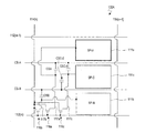
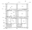
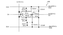
図4〜図7には、本発明による実施形態の液晶表示装置が有する行列状に配列された画素のうち、m行n列の画素のTFT基板上の構造を模式的に示している。以下の図面において、共通する構成要素は共通の参照符号で説明を省略することがある。ここで、「画素」とは、液晶表示装置が表示を行う最小単位を指し、カラー表示装置の場合は、個々の色(典型的にはR、GまたはB)を表示する「絵素(またはドット)」に対応する。 4 to 7 schematically show the structures on the TFT substrate of pixels in m rows and n columns among the pixels arranged in a matrix in the liquid crystal display device according to the embodiment of the present invention. In the following drawings, common constituent elements may be omitted with common reference numerals. Here, the “pixel” refers to the smallest unit on which the liquid crystal display device performs display. In the case of a color display device, “pixel” (or R, G, or B) that displays individual colors (typically R, G, or B). Dot).
図4に示す液晶表示装置100Aの画素においては、副画素SP−A、SP−CおよびSP−Bを列方向に沿ってこの順に配列している。すなわち、副画素の輝度順(ここでは上から降順)に配列されている。次のフレームにおいてもこの輝度の関係(画素内における副画素の輝度順位)は維持されるとともに、各副画素の液晶容量に印加される電圧の極性が反転するので、長期間にわたってDC電圧が印加されることを防止できる。なお、副画素SP−AとSP−Bとの輝度順位が入れ替わるようにVCS−AとVCS−Bの信号波形を調整してもよく、このときも副画素の輝度順(ここでは上から昇順)に配列されていることに代わりが無い。
In the pixel of the liquid
図4に示すように、第1副画素SP−Aは第1副画素電極111aによって規定される領域に対応して形成され、第2副画素SP−Bは第2副画素電極111bによって規定される領域に対応して形成され、第3副画素SP−Cは、第3副画素電極111cによって規定される領域に対応して形成されている。
As shown in FIG. 4, the first subpixel SP-A is formed corresponding to a region defined by the
(m、n)画素はGバスライン112(m)とSバスライン114(n)に接続されたTFT116a、116bおよび116cによって駆動される。TFT116aのドレイン電極はドレイン引出し配線117aを介して第1副画素電極111aに接続されている。TFT116bのドレイン電極はドレイン引出し配線117bを介して第2副画素電極111bに接続されており、TFT116cのドレイン電極はドレイン引出し配線117cを介して第3副画素電極111cに接続されている。副画素電極111a、111bおよび111cは、液晶層(不図示)と、液晶層を介して対向するように配置されている共通の対向電極(不図示)とによって、液晶容量を構成する。すなわち、第1副画素電極111aは、図1中のCLC−Aを構成し、第2副画素電極111bはCLC−Bを構成し、第3副画素電極111cはCLC−Cを構成している。対向電極は複数の画素に共通に設けられ、典型的には、全ての画素に対して共通であるが、必要に応じて複数に分割されることもある。
The (m, n) pixel is driven by
m行の画素内には、2本のCSバスライン(=補助容量配線)CS−AおよびCS−Bが通っている。第1副画素SP−Aは、1つの補助容量CSA(図1中のCCS−A)を有している。補助容量CSAの一方の電極(補助容量対向電極)はCSバスラインCS−Aに接続されており、他方の電極(補助容量電極)はドレイン引出し配線117aに接続されている。これら一対の電極と、これら一対の電極の間の絶縁層(例えばゲート絶縁層)によって補助容量CSAが構成されている。同様に、第2副画素SP−Bは、1つの補助容量CSB(図1中のCCS−B)を有している。補助容量CSBの一方の電極(補助容量対向電極)はCSバスラインCS−Bに接続されており、他方の電極(補助容量電極)はドレイン引出し配線117bに接続されている。これら一対の電極と、これら一対の電極の間の絶縁層(例えばゲート絶縁層)によって補助容量CSBが構成されている。これらに対し、第3副画素SP−Cは、2つの補助容量CSC−1およびCSC−2(図1中のCCS−C1およびCCS−C2)を有している。補助容量CSC−1の一方の電極(補助容量対向電極)はCSバスラインCS−Aに接続されており、補助容量CSC−2の一方の電極(補助容量対向電極)はCSバスラインCS−Bに接続されている。補助容量CSC−1およびCSC−2の他方の電極(補助容量電極)はいずれもドレイン引出し配線117cに接続されている。これら二対の電極と、これら二対の電極のそれぞれの間の絶縁層(例えばゲート絶縁層)によって補助容量CSC−1およびCSC−2が構成されている。
Two CS bus lines (= auxiliary capacitance lines) CS-A and CS-B pass through m rows of pixels. The first subpixel SP-A has one auxiliary capacitor CSA (CCS-A in FIG. 1). One electrode (auxiliary capacitor counter electrode) of the auxiliary capacitor CSA is connected to the CS bus line CS-A, and the other electrode (auxiliary capacitor electrode) is connected to the
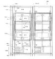
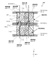
次に、図5に示す液晶表示装置100Bの画素分割構造を説明する。
Next, a pixel division structure of the liquid
液晶表示装置100Bの画素は、3つの副画素SP−A、SP−BおよびSP−Cの内のSP−BおよびSP−Cがそれぞれ2つの領域(SP−B1とSP−B2およびSP−C1とSP−C2)を有し、且つ、それぞれの副画素の2つの領域は第1副画素SP−Aを挟むように配置されている。列方向には、SP−B2(暗副画素)、SP−C2(中副画素)、SP−A(明副画素)、SP−C1(中副画素)およびSP−B1(暗副画素)の順で配列されており、次のフレームにおいてもこの輝度の関係(画素内における副画素の輝度順位)は維持されるとともに、各副画素の液晶容量に印加される電圧の極性が反転するので、長期間にわたってDC電圧が印加されることを防止できる。なお、SP−AとSP−B1およびSP−B2との輝度順位が入れ替わるようにVCS−AとVCS−Bの信号波形を調整してもよい。
The pixel of the liquid
第2副画素の2つの領域SP−B1およびSP−B2は、それぞれ2つの副画素電極111b1および111b2に対応して形成されており、これらはドレイン引出し配線117bbによって互いに接続されており、ドレイン引出し配線117bbはドレイン引出し配線117bを介してTFT116bのドレイン電極に接続されている。同様に、第3副画素の2つの領域SP−C1およびSP−C2は、それぞれ2つの副画素電極111c1および111c2に対応して形成されており、これらはドレイン引出し配線117ccによって互いに接続されており、ドレイン引出し配線117ccはドレイン引出し配線117cを介してTFT116cのドレイン電極に接続されている。
The two regions SP-B1 and SP-B2 of the second subpixel are formed corresponding to the two subpixel electrodes 111b1 and 111b2, respectively, which are connected to each other by the drain lead wiring 117bb. The wiring 117bb is connected to the drain electrode of the
その他の接続関係は、上記の液晶表示装置100Aと同じであるので説明を省略する。液晶表示装置100Bの画素における第2副画素の2つの領域SP−B1およびSP−B2は互いに等価であるとともに、液晶表示装置100Aの第2副画素SP−Bと等価である。また、液晶表示装置100Bの画素における第3副画素の2つの領域SP−C1およびSP−C2は互いに等価であるとともに、液晶表示装置100Aの第3副画素SP−Cと等価である。
Since other connection relations are the same as those of the liquid
液晶表示装置100Bのように、副画素をさらに空間的に分割することによって、画素内で異なる輝度を呈する領域がさらに細分化されるので、画像のざらつきが抑制され、均質性が向上する。特に、大型の液晶表示装置(例えば50型以上)においては画素サイズが大きいために、マルチ画素構造を採用すると、画素内の輝度の分布がざらつきとして感じられることがあり、これを防止するために有効である。
As in the liquid
次に、図6に示す液晶表示装置100Cの画素分割構造を説明する。
Next, a pixel division structure of the liquid
液晶表示装置100Cの画素は、3つの副画素SP−A、SP−BおよびSP−Cの内のSP−BおよびSP−Cがそれぞれ第1副画素SP−Aを挟むように配置された2つの領域を有している点で、図5に示した液晶表示装置100Bと共通している。液晶表示装置100Bにおいて、第3副画素の2つの領域SP−C1およびSP−C2をそれぞれ構成する副画素電極111c1および111c2がドレイン引出し配線を介して互いに電気的に接続されていたのに対し、液晶表示装置100Cでは1つのコの字状(U字状または馬蹄形状)の副画素電極111cとして形成されている点が異なる。その他の点は液晶表示装置100Bと同じなので説明を省略する。
The pixels of the liquid
次に、図7に示す液晶表示装置100Dの画素分割構造を説明する。
Next, a pixel division structure of the liquid
液晶表示装置100Dの画素は、3つの副画素SP−A、SP−BおよびSP−Cの内のSP−BおよびSP−Cがそれぞれ第1副画素SP−Aを挟むように配置された2つの領域を有している点で、図5に示した液晶表示装置100Bおよび図6に示した液晶表示装置100Cと共通している。さらに、第3副画素の2つの領域を構成する副画素電極が1つのコの字状の副画素電極111cとして形成されている点で図6に示した液晶表示装置100Cと共通している。液晶表示装置100Cにおいて、第2副画素の2つの領域SP−B1およびSP−B2をそれぞれ構成する副画素電極111b1および111b2がドレイン引出し配線を介して互いに電気的に接続されていたのに対し、液晶表示装置100Dでは1つのコの字状の副画素電極111bとして形成されている点が異なる。その他の点は液晶表示装置100Cと同じなので説明を省略する。
The pixels of the liquid
液晶表示装置100Cおよび100Dのように、副画素を2つの領域に分割した際に、副画素電極をコの字状にすることによって、ドレイン引出し配線の引き回しを単純にすることができる。また、ここでは、第2副画素電極111bおよび第3副画素電極111cをコの字状の電極とした例を示したが、これに限られず、後述するように、環状(口の字状または角張ったO字状)の電極としてもよい。環状の電極とすると、寄生容量(例えばCsd)を容易に調整することができる。
When the subpixel is divided into two regions as in the liquid
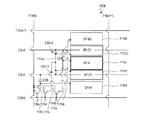
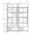
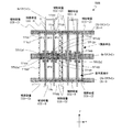
次に、図8〜図12を参照して、本発明による液晶表示装置の画素の具体的な構成を説明する。図8〜図12は、m行n列およびm行n+1列の2つの画素のTFT基板上の構造を模式的に示している。典型的なドット反転駆動を行う場合、m行n列(以下(m、n)と表記する)の画素に信号電圧が正極性(対向電圧を基準としたときの極性)で書き込まれているとき、(m、n+1)画素は負極性で書き込まれる。このとき、(m、n)画素の副画素SP−Aが明副画素、副画素SP−Bが暗副画素、副画素SP−Cが中副画素となる場合、(m、n+1)画素の副画素SP−Aが暗副画素、副画素SP−Bが明副画素、副画素SP−Cが中副画素となるように駆動され得る。 Next, a specific configuration of the pixel of the liquid crystal display device according to the present invention will be described with reference to FIGS. 8 to 12 schematically show structures on the TFT substrate of two pixels of m rows and n columns and m rows and n + 1 columns. When performing typical dot inversion driving, when a signal voltage is written to a pixel of m rows and n columns (hereinafter referred to as (m, n)) with positive polarity (polarity with reference to the counter voltage). , (M, n + 1) pixels are written with negative polarity. At this time, when the subpixel SP-A of the (m, n) pixel is the bright subpixel, the subpixel SP-B is the dark subpixel, and the subpixel SP-C is the middle subpixel, the (m, n + 1) pixel The sub-pixel SP-A can be driven to be a dark sub-pixel, the sub-pixel SP-B to be a bright sub-pixel, and the sub-pixel SP-C to be a middle sub-pixel.
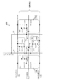
図8に示す液晶表示装置200Aは、図4に示した液晶表示装置100Aと同じ等価回路で表され、副画素の配置も同じである。
The liquid
(m、n)画素に注目する。(m、n)画素はゲートバスライン112(m)とソースバスライン114(n)に接続されたTFT116a、116bおよび116cによって駆動される。TFT116aのドレイン電極はドレイン引出し配線117aを介してコンタクト部119aにおいて第1副画素電極111aに接続されている。TFT116bのドレイン電極はドレイン引出し配線117bを介して、コンタクト部119bにおいて第2副画素電極111bに接続されており、TFT116cのドレイン電極はドレイン引出し配線117cを介して、コンタクト部119c1および119c2において第3副画素電極111cに接続されている。副画素電極111a、111bおよび111cは、液晶層(不図示)と、液晶層を介して対向するように配置されている対向電極(不図示)とによって、それぞれ液晶容量CLC−A、CLC−BおよびCLC−C(図1参照)を構成する。
Focus on (m, n) pixels. The (m, n) pixel is driven by
ここで、ソースバスライン114(n)はn列の副画素電極111a、111bおよび111cと部分的に重なっている。ソースバスライン114(n)と副画素電極111a、111bおよび111cとの間の寄生容量(Csd)を十分に小さくできるように、これらの間には樹脂で形成された層間絶縁膜、例えば2.5μm程度のアクリル系樹脂、が設けられている。言い換えると、層間絶縁膜を設けることによって、副画素電極111a、111bおよび111cをソースバスライン114(n)と重なるように設けることが可能となり、画素開口率を向上させることができる。
Here, the source bus line 114 (n) partially overlaps the n columns of
TFT116a、116bおよび116cはボトムゲート構造を有しており、それぞれ、ゲートバスライン112(m)の延設部として形成されたゲート電極と、その上に形成された半導体層と、半導体層のソースおよびドレイン領域に形成されたソース電極およびドレイン電極とを有している。ソース電極はソースバスライン114(n)の延設部として形成されている。TFT116a、116bおよび116cのドレイン電極はそれぞれドレイン引出し配線117a、117bおよび117cと一体に形成されている。これら全てを覆うように層間絶縁膜(不図示)が設けられており、層間絶縁膜上に副画素電極111a、111bおよび111cが形成されている。層間絶縁膜に形成されたコンタクトホール内のコンタクト部119aにおいてドレイン引出し配線117aと副画素電極111aとが接続されており、コンタクト部119bにおいてドレイン引出し配線117bと副画素電極111bとが接続されており、コンタクト部119c1および119c2においてドレイン引出し配線117cと副画素電極111cとが接続されている。
The
次に、(m、n)画素における補助容量の構成を説明する。m行の画素内には、2本のCSバスライン(=補助容量配線)113−1および113−2が通っている。CSバスライン113−1は図4(または図1)中のCSバスラインCS−Aに対応し、CSバスライン113−2はCSバスラインCS−Bに対応する。 Next, the configuration of the auxiliary capacitor in the (m, n) pixel will be described. Two CS bus lines (= auxiliary capacitance lines) 113-1 and 113-2 pass through the m rows of pixels. The CS bus line 113-1 corresponds to the CS bus line CS-A in FIG. 4 (or FIG. 1), and the CS bus line 113-2 corresponds to the CS bus line CS-B.
副画素SP―Aの補助容量(図4中のCSA)は、ドレイン引出し配線117aがCSバスライン113−1と重なる部分(コンタクト部119a付近)に形成されている。副画素SP−Bの補助容量(図4中のCSB)は、ドレイン引出し配線117bがCSバスライン113−2と重なる部分(コンタクト部119b付近)に形成されている。
The auxiliary capacitance (CSA in FIG. 4) of the sub-pixel SP-A is formed in a portion (near the
副画素SP−Cは2つの補助容量(図4中のCSC−1およびCSC−2)を有している。補助容量CSC−1はドレイン引出し配線117cがCSバスライン113−1と重なる部分(コンタクト部119c2付近)に形成されており、補助容量CSC−2はドレイン引出し配線117cがCSバスライン113−2と重なる部分(コンタクト部119c1付近)に形成されている。CSバスライン113−1および113−2はいずれもゲートバスライン112(m)と同じ導電層で形成されており、ゲート絶縁膜(不図示)によって覆われている。補助容量CSC−1およびCSC−2の誘電体層はいずれもゲート絶縁膜であり、補助容量CSC−1およびCSC−2の容量値はそれぞれ電極の面積に比例する。ここでは図8に示すように、補助容量CSC−1およびCSC−2の容量値は互いにほぼ等しい。
The subpixel SP-C has two auxiliary capacitors (CSC-1 and CSC-2 in FIG. 4). The auxiliary capacitor CSC-1 is formed in a portion where the
図9に示す液晶表示装置200Bは、図5に示した液晶表示装置100Bと同じ等価回路で表され、副画素の配置も同じである。液晶表示装置200Bの画素は、3つの副画素SP−A、SP−BおよびSP−Cの内のSP−BおよびSP−Cがそれぞれ2つの領域(SP−B1とSP−B2およびSP−C1とSP−C2)を有し、且つ、それぞれの副画素の2つの領域は第1副画素SP−Aを挟むように配置されている。以下では、液晶表示装置200Aと異なる第2副画素SP−Bおよび第3副画素SP−Cの構成を説明する。
The liquid
第2副画素の2つの領域SP−B1およびSP−B2は、それぞれ2つの副画素電極111b1および111b2に対応して形成されている。副画素電極111b1はコンタクト部119b1においてドレイン引出し配線117bと接続されており、副画素電極111b2はコンタクト部119b2においてドレイン引出し配線117bと接続されている。第3副画素の2つの領域SP−C1およびSP−C2は、それぞれ2つの副画素電極111c1および111c2に対応して形成されている。副画素電極111c1はコンタクト部119c1においてドレイン引出し配線117cと接続されており、副画素電極111c2はコンタクト部119c2においてドレイン引出し配線117cと接続されている。
The two regions SP-B1 and SP-B2 of the second subpixel are formed corresponding to the two subpixel electrodes 111b1 and 111b2, respectively. The subpixel electrode 111b1 is connected to the
また、2つのCSバスライン113−1および113―2は、それぞれ環状部と非環状部とを有している。CSバスライン113−1および113―2の環状部はソースバスライン114(n)と114(n+1)と重ならないように、これらの内側に形成されている。CSバスライン113−1および113―2の非環状部は、行方向に隣接する画素間に存在するソースバスラインと交差し、行方向に隣接する環状部を互いに連結している。CSバスライン113−2の環状部の内側に存在する副画素電極111c1の部分が副画素SP―C1の表示に寄与し、CSバスライン113−1の環状部の内側に存在する副画素電極111c2の部分が副画素SP―C2の表示に寄与する。また、2つのCSバスライン113−1および113―2の環状部は、隣接する副画素間にも存在し、この領域を遮光する機能をも果たしている。 The two CS bus lines 113-1 and 113-2 each have an annular portion and a non-annular portion. The annular portions of the CS bus lines 113-1 and 113-2 are formed inside these so as not to overlap the source bus lines 114 (n) and 114 (n + 1). The non-annular portions of the CS bus lines 113-1 and 113-2 intersect with source bus lines existing between pixels adjacent in the row direction, and connect the annular portions adjacent in the row direction to each other. The portion of the subpixel electrode 111c1 existing inside the annular portion of the CS bus line 113-2 contributes to the display of the subpixel SP-C1, and the subpixel electrode 111c2 existing inside the annular portion of the CS bus line 113-1. This part contributes to the display of the sub-pixel SP-C2. In addition, the annular portions of the two CS bus lines 113-1 and 113-2 exist between adjacent sub-pixels, and also serve to shield this area.
副画素SP−Aの補助容量は、バスライン113−1の環状部とドレイン引出し配線117aとが重なる領域(コンタクト部119a近傍)に形成されている。副画素SP−Bの補助容量は、バスライン113−2の環状部とドレイン引出し配線117bとが重なる領域に形成されている。ただし、(m、n+1)画素について見ると、副画素SP−Aの補助容量は、バスライン113−2の環状部とドレイン引出し配線117aとが重なる領域に形成されており、副画素SP−Bの補助容量(SP−B1およびSP−B2に対して1つの補助容量)は、バスライン113−1の環状部とドレイン引出し配線117bとが重なる領域に形成されている。このように配置することによって、ドット反転駆動を行った場合においても、(m、n)画素と(m、n+1)画素とにおける副画素の輝度の順位を同じにできる。このことは、例えば(m、n)画素でSP−Aを明副画素とした場合、(m、n+1)画素においてもSP−Aを明副画素とすることができるので、比較的認識されやすい明副画素の位置が画素ごとに異なることで画像のざらつきとして感じられることがあるような場合に、これを抑制することができる。
The auxiliary capacitance of the sub-pixel SP-A is formed in a region (near the
なお、ドレイン引出し配線117aおよび117bは、2つのCSバスライン113−1および113−2の非環状部とそれぞれ同じ回数だけ交差するように配置されており、補助容量を形成する部分以外の容量への寄与を相殺している。また、副画素SP−Cの2つの補助容量の内の一方は、CSバスライン113−1とドレイン引出し配線117cとが重なる領域(コンタクト部119c2近傍)に形成されており、他方は、CSバスライン113−2とドレイン引出し配線117cとが重なる領域(コンタクト部119c1近傍)に形成されている。ここでも、副画素SP−Cの2つの補助容量の静電容量値はほぼ同じに設定されている。
The
図10に示す液晶表示装置200Cは、図6に示した液晶表示装置100Cと同じ等価回路で表され、副画素の配置も同じである。図9に示した液晶表示装置200Bと比較すると、液晶表示装置200Bにおいて、第3副画素SP−Cの2つの領域SP−C1およびSP−C2をそれぞれ構成する副画素電極111c1および111c2がドレイン引出し配線117cを介して互いに電気的に接続されていたのに対し、液晶表示装置200Cでは1つのコの字状(U字状または馬蹄形状)の副画素電極111cとして形成されている点が異なる。また、コの字状の副画素電極111cにおける2つの領域を連結する部分と副画素電極111aとの間隙は、ドレイン引出し配線117aで遮光するように構成されている。
A liquid
図11に示す液晶表示装置200C’は、図10に示した液晶表示装置200Cにおけるコの字状の副画素電極111cを環状(口の字状または角張ったO字状)の副画素電極111cとした点において異なる。環状の副画素電極111cと、その開口部内に配置される副画素電極111aとの間隙は、ドレイン引出し配線117aおよび117bで遮光するように構成されている。副画素電極111cを環状とすると、副画素電極111cをコの字状とするよりもソース・ドレイン間の寄生容量(Csd)を容易に調整できるという利点が得られる。
A liquid
図12に示す液晶表示装置200Dは、図7に示した液晶表示装置100Dの変形例であり、液晶表示装置100Dのコの字状の副画素SP−Cを環状に改変したものに対応する。図11に示した液晶表示装置200C’と比較すると、液晶表示装置200C’において、第2副画素SP−Bの2つの領域SP−B1およびSP−B2をそれぞれ構成する副画素電極111b1および111b2がドレイン引出し配線117bを介して互いに電気的に接続されていたのに対し、液晶表示装置200Dでは1つの環状の副画素電極111bとして形成されている点が異なる。また、副画素電極111bと副画素電極111cとの間隙は、ソースバスライン114(n)および114(n+1)によって遮光されるように構成されている。
A liquid crystal display device 200D illustrated in FIG. 12 is a modification of the liquid
次に、図13および図14を参照して、本発明による実施形態のMVA型の液晶表示装置の具体的な構成を説明する。MVA型の液晶表示装置は、良く知られているように、誘電異方性が負のネマチック液晶材料を用いた垂直配向モードであり、各画素内に、電圧印加時の液晶分子の配向方向が互いに異なる4つの方向(任意の2つの方向の差が約90°の倍数)であるドメイン(4分割ドメイン)を有し、ノーマリブラックモードで表示を行う表示装置である。なお、MVA型液晶表示装置にマルチ画素構造を適用する場合、視野角特性の観点から、各副画素について4つのドメインを形成することが好ましい。 Next, a specific configuration of the MVA type liquid crystal display device according to the embodiment of the present invention will be described with reference to FIGS. As is well known, the MVA type liquid crystal display device is a vertical alignment mode using a nematic liquid crystal material having a negative dielectric anisotropy, and the alignment direction of liquid crystal molecules when a voltage is applied is set in each pixel. The display device has a domain (four divided domains) having four directions different from each other (a difference between arbitrary two directions is a multiple of about 90 °) and performs display in a normally black mode. Note that when a multi-pixel structure is applied to the MVA liquid crystal display device, it is preferable to form four domains for each sub-pixel from the viewpoint of viewing angle characteristics.
図13に示す液晶表示装置300Bは、図5に示した液晶表示装置100Bおよび図9に示した液晶表示装置200Bと同じ等価回路で表され、副画素の配置も同じである。以下の説明では、液晶表示装置200Bの構造と共通する点の説明を省略する。
The liquid
副画素電極111aに形成されたスリットSLa、副画素電極111aと副画素電極111c1および111c2との間隙、副画素電極111c1と副画素電極111b1との間隙、副画素電極111c2と副画素電極111b2との間隙が、斜め電界を生成し、マルチドメイン構造を形成するための配向規制手段(画素電極に形成されたスリット)として機能する。スリットSLaおよび隣接する副画素電極間の間隙は、マトリクス状に配列された列方向に対して約45°の角度で交差する方向に延びており、互いに略直交する方向に延びている。液晶パネルを介したクロスニコルに配置される偏光板の偏光軸(透過軸)は列方向および行方向に直交または平行であり、上述のように配置されたスリットおよび副画素電極間の間隙は、電圧印加時における液晶分子の配向方向を偏光軸に対して略45°方向に規制するように作用する。なお、対向基板側には、互いに隣接し互いに平行なスリットと副画素電極の間隙との間、または、互いに隣接し互いに平行な副画素電極の間隙の間に、その間隔を略2等分する位置に、それらに平行な配向規制手段が設けられる。対向基板に設けられる配向規制手段は、対向電極に設けられるスリットであってもよいし、対向電極の液晶層側に設けられる誘電体突起(リブ)であってもよい。なお、誘電体突起の誘電率は液晶層の誘電率よりも低いことが好ましい。
The slit SLa formed in the
液晶表示装置300Bにおける補助容量は、CSバスラインの延設部とドレイン引出し配線とが重なる領域に形成されている。例えば、CSバスライン113−1は環状の延設部113−1Eを有しており、環状の延設部113−1Eの中央をブリッジする部分がドレイン引出し配線117cと重なる部分に、副画素SP−Cが有する2つの補助容量の内の一方の補助容量が形成されている。同様に、CSバスライン113−2は環状の延設部113−2Eを有しており、環状の延設部113−2Eの中央をブリッジする部分がドレイン引出し配線117cと重なる部分に、副画素SP−Cが有する2つの補助容量の内の他方の補助容量が形成されている。また、環状の延設部113−1Eおよび113−2Eの環部分は、隣接する副画素電極の間隙を遮光するように配置されている。副画素SP−Aの補助容量は、CSバスライン113−1とドレイン引出し配線117aとが重なる部分(副画素電極111c2の下部)で形成されており、副画素SP−Bの補助容量は、CSバスライン113−2とドレイン引出し配線117bとが重なる部分(副画素電極111c1の下部)で形成されている。
The auxiliary capacitor in the liquid
図14に示す液晶表示装置300Cは、図6に示した液晶表示装置100Cおよび図10に示した液晶表示装置200Cと同じ等価回路で表され、副画素の配置も同じである。図13に示した液晶表示装置300Bと比較すると、液晶表示装置300Bにおいて、副画素電極111c1および111c2がドレイン引出し配線117cを介して互いに電気的に接続されていたのに対し、液晶表示装置300Cでは1つのコの字状(U字状または馬蹄形状)の副画素電極111cとして形成されている点が異なる。また、コの字状の副画素電極111cにおける2つの領域を連結する部分と副画素電極111aとの間隙は、ドレイン引出し配線117aで遮光するように構成されている。
A liquid
また、液晶表示装置300Cは第3副画素の一方の領域SP−C2に、ドレイン引出し配線と同じ導電層で形成されたドレイン浮島117c’を有している。ドレイン浮島117c’はコンタクト部119c2において副画素電極111cと接続されている。ドレイン浮島117c’とCSバスラインの環状延設部113−1Eの一部とが重なる領域に、副画素SP−Cが有する2つの補助容量の一方が形成されている。副画素SP−Cが有する2つの補助容量の他方は、ドレイン引出し配線117cがCSバスライン113−2の環状延設部113−2Eと重なる領域に形成されている。
In addition, the liquid
なお、ここで、補助容量を形成する部分を、隣接する副画素電極の間隙の方向に平行に設けている理由は、マルチドメイン構造を得るために対向基板側に形成される配向規制手段(電極スリットまたは誘電体突起)と重ねることにより、光漏れを防止するためである。 Here, the reason that the portion for forming the auxiliary capacitance is provided in parallel to the direction of the gap between the adjacent subpixel electrodes is that the orientation regulating means (electrode) formed on the counter substrate side in order to obtain a multi-domain structure. This is for preventing light leakage by overlapping with a slit or a dielectric protrusion.
次に、画素内における副画素の好ましい配列をγ特性の観点から説明する。 Next, a preferable arrangement of sub-pixels within a pixel will be described from the viewpoint of γ characteristics.
まず、図15(a)および(b)を参照して、2分割構造のγ特性の視野角依存性について説明する。ここでは、明副画素(SP−A)を2つの領域SP−A1およびSP−A2に分割し、暗副画素(SP−B)を2つの領域SP−B1およびSP−B2に分割した例を示しているが、γ特性は2分割構造であれば、各副画素を複数の領域に分割しても変わらない。ただし、図15(a)に示したように各副画素を2つの領域に分割すれば、例えば52型(画素配列ピッチ:行方向200μm、列方向600μm)を超える超大型の液晶表示装置において、中間調を表示した際に、明副画素と暗副画素との市松状の配列が表示のざらつきとして視認され難くなる。 First, with reference to FIGS. 15A and 15B, the viewing angle dependence of the γ characteristic of the two-part structure will be described. In this example, the bright subpixel (SP-A) is divided into two regions SP-A1 and SP-A2, and the dark subpixel (SP-B) is divided into two regions SP-B1 and SP-B2. As shown, if the γ characteristic is a two-divided structure, it does not change even if each subpixel is divided into a plurality of regions. However, if each sub-pixel is divided into two regions as shown in FIG. 15A, in an ultra-large liquid crystal display device exceeding 52 type (pixel arrangement pitch: 200 μm in the row direction, 600 μm in the column direction), for example, When halftones are displayed, a checkered arrangement of bright and dark subpixels becomes difficult to be visually recognized as display roughness.
2分割構造(2つのVT特性の重ね合わせを実現するので2VT構造ともいう。)のγ特性の視野角依存性を図15(b)に示す。図15(b)は、横軸が正面における階調で、縦軸が左右(偏光軸に平行または直交)における斜め視野角(表示面法線から45°)での階調を示すグラフである。2分割構造では、図15(b)に示すように、100/255階調付近に窪みが形成され、滑らかな変化が得られない。このγ特性の視野角依存性を改善するためには、分割数を3以上とする必要がある。 FIG. 15B shows the viewing angle dependency of the γ characteristic of the two-divided structure (also referred to as a 2VT structure because two VT characteristics are superimposed). FIG. 15B is a graph showing the gray level at the front surface and the vertical axis at the oblique viewing angle (45 ° from the normal to the display surface) on the left and right (parallel or orthogonal to the polarization axis). . In the two-divided structure, as shown in FIG. 15B, a depression is formed in the vicinity of 100/255 gradation, and a smooth change cannot be obtained. In order to improve the viewing angle dependency of the γ characteristic, the number of divisions needs to be 3 or more.
次に、図16および図17を参照して、3分割構造(3VT構造)とした場合の好ましい副画素の配列およびγ特性の視野角依存性について説明する。 Next, with reference to FIG. 16 and FIG. 17, a preferred subpixel arrangement and viewing angle dependency of γ characteristics in the case of a three-division structure (3VT structure) will be described.
図16(a)に示すように、明副画素SP−A、暗副画素SP−Bおよび中副画素SP−C(SP−C1およびSP−C2)の面積比を1:1:2とした場合のγ特性の視野角依存性を図16(b)に示す。図16(b)を図15(b)と比較すれば明らかなように、100/255階調付近の滑らかさが改善されている。 As shown in FIG. 16A, the area ratio of the bright subpixel SP-A, the dark subpixel SP-B, and the middle subpixel SP-C (SP-C1 and SP-C2) is 1: 1: 2. FIG. 16B shows the viewing angle dependency of the γ characteristic in this case. As apparent from a comparison of FIG. 16B with FIG. 15B, the smoothness near the 100/255 gradation is improved.
また、図17(a)に示すように、明副画素SP−A、暗副画素SP−Bおよび中副画素SP−C(SP−C1およびSP−C2)の面積比を1:1:1とすると、図17(b)に示すように、100/255階調付近の滑らかさがさらに改善される。このように、γ特性の視野角依存性の観点からは、明副画素、中副画素および暗副画素の面積比は1:1:1であることが好ましい。 Also, as shown in FIG. 17A, the area ratio of the bright subpixel SP-A, the dark subpixel SP-B, and the middle subpixel SP-C (SP-C1 and SP-C2) is 1: 1: 1. Then, as shown in FIG. 17B, the smoothness near 100/255 gradation is further improved. Thus, from the viewpoint of the viewing angle dependency of the γ characteristic, the area ratio of the bright subpixel, the middle subpixel, and the dark subpixel is preferably 1: 1: 1.
また、表示のざらつきを低減するという観点からは、明副画素を画素の中心に配置することが好ましい。また、ドット反転駆動等において、副画素間の輝度順位を入れ替えることを考慮すると、明副画素と暗副画素とを入れ替えることが好ましい。従って、少なくとも明副画素と暗副画素の面積は等しいことが好ましい。さらに、表示のざらつきを低減するという観点からは、明副画素と暗副画素とを近接させて画素の中央に配置することが好ましい。なお、図5等に示した液晶表示装置において、画素内において中副画素と暗副画素とを入れ替えることは、容易に行うことができる。 Further, from the viewpoint of reducing display roughness, it is preferable to arrange the bright sub-pixel at the center of the pixel. In addition, in the dot inversion driving or the like, it is preferable to replace the bright subpixel and the dark subpixel in consideration of switching the luminance order between the subpixels. Therefore, it is preferable that at least the areas of the bright subpixel and the dark subpixel are equal. Furthermore, from the viewpoint of reducing display roughness, it is preferable that the bright subpixel and the dark subpixel are arranged close to each other at the center of the pixel. Note that in the liquid crystal display device illustrated in FIG. 5 and the like, the middle subpixel and the dark subpixel can be easily replaced in the pixel.
また、γ特性の波長依存性を考慮すると、青画素のセルギャップ(液晶層の厚さ)を他の色画素(典型的には緑画素および赤画素)よりも小さくすることが好ましい。 In consideration of the wavelength dependence of the γ characteristic, it is preferable to make the cell gap (the thickness of the liquid crystal layer) of the blue pixel smaller than other color pixels (typically green pixel and red pixel).
図17(b)において、γ特性の視野角依存性を赤(R)、緑(G)および青(B)ごとに示したが、青(B)の視野角依存性は、赤(R)および緑(G)よりも大きいことが分かる。これは、液晶層のリタデーション(複屈折率)の波長分散に起因する。図17(b)は、セルギャップ(液晶層の厚さ)をR画素、G画素およびB画素の全てについて3.4μmとした場合の階調特性を示したが、B画素のセルギャップだけを3.0μmとすることによって、B画素のγ特性が他の色画素のγ特性に近づき、全体として、γ特性の視野角依存性が改善される。 In FIG. 17B, the viewing angle dependence of the γ characteristic is shown for each of red (R), green (G), and blue (B). The viewing angle dependence of blue (B) is red (R). And larger than green (G). This is due to the wavelength dispersion of retardation (birefringence) of the liquid crystal layer. FIG. 17B shows the gradation characteristics when the cell gap (thickness of the liquid crystal layer) is 3.4 μm for all of the R pixel, the G pixel, and the B pixel, but only the cell gap of the B pixel is shown. By setting the thickness to 3.0 μm, the γ characteristic of the B pixel approaches that of other color pixels, and the viewing angle dependency of the γ characteristic is improved as a whole.
なお、上述したように、補助容量の形成にGバスラインを用いてもよい。 As described above, the G bus line may be used for forming the auxiliary capacitor.
図18に、本発明による実施形態の液晶表示装置400Aの等価回路を模式的に示す。液晶表示装置400Aにおいて1つの画素は、第1、第2、第3副画素SP−A、SP−B、SP−Cを有している。第1、第2、第3副画素SP−A、SP−B、SP−Cおよび2つのCSバスラインCS−A、CS−Bは隣接する2つのGバスラインの間に配置されている。液晶表示装置400Aでは、Gバスラインの数は画素の行数と対応しているが、Gバスラインは、画素を選択するだけでなく、列方向に隣接する画素の第3副画素SP−Cの補助容量に接続されている。このため、各画素に2つのGバスラインが関連付けられている。
FIG. 18 schematically shows an equivalent circuit of the liquid
図18にはm行の画素を示しており、m−1行のGバスラインおよびm行のGバスラインを、それぞれGバスラインG(m−1)およびGバスラインG(m)と示している。第1、第2、第3副画素SP−A、SP−B、SP−CのTFT−A、TFT−B、TFT−Cのゲート電極はGバスラインG(m)と接続されている。また、図18には図示していないが、同様に、m−1行の3つの副画素のTFTのゲート電極はGバスラインG(m−1)と接続されている。 FIG. 18 shows m rows of pixels, and m−1 rows of G bus lines and m rows of G bus lines are denoted as G bus lines G (m−1) and G bus lines G (m), respectively. ing. The gate electrodes of the TFT-A, TFT-B, and TFT-C of the first, second, and third subpixels SP-A, SP-B, and SP-C are connected to the G bus line G (m). Although not shown in FIG. 18, similarly, the gate electrodes of the TFTs of the three subpixels in the (m−1) th row are connected to the G bus line G (m−1).
液晶表示装置400Aにおける、2つの副画素SP−AおよびSP−Bと、TFT−AおよびTFT−B、Gバスライン、Sバスライン、および2本の互いに電気的に独立なCSバスラインとの間の接続関係は、図4に示した液晶表示装置100Aと基本的に同じであるため、簡単のために説明を省略する。3番目の副画素SP−Cは以下のように接続されている。
In the liquid
第3副画素SP−Cは、液晶容量CLC−Cと、補助容量CCS−G(m−1)とを有している。液晶容量CLC−Cの一方の電極(副画素電極)はTFT−Cのドレイン電極に接続されており、補助容量CCS−G(m−1)の一方の電極もTFT−Cのドレイン電極に接続されている。液晶容量CLC−Cの他方の電極(対向電極)は、他の液晶容量CLC−A、CLC−Bと共通の対向電極で構成されている。補助容量CCS−G(m−1)の他方の電極(補助容量対向電極)はGバスラインG(m−1)に接続されている。 The third subpixel SP-C has a liquid crystal capacitor CLC-C and an auxiliary capacitor CCS-G (m−1). One electrode (subpixel electrode) of the liquid crystal capacitor CLC-C is connected to the drain electrode of the TFT-C, and one electrode of the auxiliary capacitor CCS-G (m−1) is also connected to the drain electrode of the TFT-C. Has been. The other electrode (counter electrode) of the liquid crystal capacitor CLC-C is composed of a common electrode common to the other liquid crystal capacitors CLC-A and CLC-B. The other electrode (auxiliary capacitor counter electrode) of the auxiliary capacitor CCS-G (m−1) is connected to the G bus line G (m−1).
第1副画素SP−Aの液晶容量CLC−Aは補助容量CCS−Aを介してCSバスラインCS−Aによる突き上げ(または突き下げ)の作用を受け、また、第2副画素SP−Bの液晶容量CLC−Bは補助容量CCS−Bを介してCSバスラインCS−Bによる突き下げ(または突き上げ)の作用を受ける。一方、GバスラインG(m)は、GバスラインG(m−1)がオフ状態になった後に選択され、次にGバスラインG(m)が選択される直前までGバスラインG(m−1)はオフ状態を維持する。なお、厳密には、GバスラインG(m−1)が選択されたときに第3副画素SP−Cの液晶容量CLC−Cは突き上げ作用を受ける。しかしながら、GバスラインG(m−1)が選択されるのは、GバスラインG(m)が選択された後一垂直走査期間経過する直前であり、GバスラインG(m−1)の選択により突き上げ作用を受けた直後にG(m)が選択され、GバスラインG(m−1)が選択されている期間は一垂直走査に比べて非常に短いため、第3副画素SP−Cの液晶容量CLC−CはGバスラインG(m−1)による作用を実質的に受けないといえる。したがって、液晶容量CLC−Cに印加される実効電圧は、液晶容量CLC−Aおよび液晶容量CLC−Bに印加される実効電圧の中間の値となる。このため、第1副画素SP−Aが暗副画素となるとき、第2副画素SP−Bは明副画素、第3副画素は中副画素となる。以上のようにして、1画素あたりのCSバスラインの本数を増加させることなく、3VT構造を実現することができる。 The liquid crystal capacitor CLC-A of the first sub-pixel SP-A is subjected to a push-up (or push-down) action by the CS bus line CS-A via the auxiliary capacitor CCS-A, and the second sub-pixel SP-B The liquid crystal capacitor CLC-B is pushed down (or pushed up) by the CS bus line CS-B via the auxiliary capacitor CCS-B. On the other hand, the G bus line G (m) is selected after the G bus line G (m-1) is turned off, and then the G bus line G (m) until just before the G bus line G (m) is selected. m-1) remains off. Strictly speaking, when the G bus line G (m−1) is selected, the liquid crystal capacitance CLC-C of the third subpixel SP-C is subjected to a pushing action. However, the G bus line G (m−1) is selected immediately before one vertical scanning period elapses after the G bus line G (m) is selected, and the G bus line G (m−1) is selected. The period during which G (m) is selected immediately after receiving the push-up action by selection and the G bus line G (m−1) is selected is much shorter than one vertical scan, and thus the third subpixel SP− It can be said that the C liquid crystal capacitor CLC-C is not substantially affected by the G bus line G (m−1). Therefore, the effective voltage applied to the liquid crystal capacitor CLC-C is an intermediate value between the effective voltages applied to the liquid crystal capacitor CLC-A and the liquid crystal capacitor CLC-B. Therefore, when the first subpixel SP-A is a dark subpixel, the second subpixel SP-B is a bright subpixel, and the third subpixel is a middle subpixel. As described above, a 3VT structure can be realized without increasing the number of CS bus lines per pixel.
また、ドレイン引出し配線は、コンタクト部において第3副画素の副画素電極と接続するとともにゲートバスラインと重なる補助容量電極を有している。液晶表示装置400Aでは、列方向に隣接する画素を選択するためのゲートバスラインの傍に第3副画素を設けているため、ドレイン引出し配線のコンタクト部と補助容量電極との間の距離を短くすることができ、ドレイン引出し配線の引き回しを単純にすることができる。また、画素の中央に明副画素を配置することができ、これにより、ジャギー(ざらつき感)の発生を抑制できる。
The drain lead wiring has a storage capacitor electrode that is connected to the subpixel electrode of the third subpixel at the contact portion and overlaps the gate bus line. In the liquid
なお、上述した液晶表示装置のCSバスラインは、1つの画素内の1つまたは複数の副画素の補助容量と接続していたが、本発明はこれに限定されない。CSバスラインは、列方向に隣接する2つの画素に属する複数の副画素の補助容量と接続してもよい。 The CS bus line of the liquid crystal display device described above is connected to the auxiliary capacitor of one or a plurality of subpixels in one pixel, but the present invention is not limited to this. The CS bus line may be connected to auxiliary capacitors of a plurality of subpixels belonging to two pixels adjacent in the column direction.
図19に、本発明による実施形態の液晶表示装置400Bの等価回路を模式的に示す。液晶表示装置400Bでは、CSバスライン(CS配線)の数は画素の行数に対応しているが、1つのCSバスラインは列方向に隣接する2つの画素に属する副画素のそれぞれの液晶容量に突き上げまたは突き下げ作用を与えており、各画素に2つのCSバスラインが関連付けられている。したがって、液晶表示装置400BのCSバスラインの数は、図18に示した液晶表示装置400Aと比べて少ない。なお、液晶表示装置400Bでは、画素の中央にゲートバスラインが配置されており、いわゆるセンターゲート構造となっている。
FIG. 19 schematically shows an equivalent circuit of the liquid
ここで、m−1行の画素に注目する。m−1行の画素の第1、第2、第3副画素SP−A、SP−B、SP−Cは、隣接する2つのCSバスラインCS−A、CS−Bの間に配置されている。第3副画素SP−Cは、液晶容量CLC−Cと、補助容量CCS−G(m−2)とを有している。液晶容量CLC−Cの一方の電極(副画素電極)はTFT−Cのドレイン電極に接続されており、補助容量CCS−G(m−2)の一方の電極もTFT−Cのドレイン電極に接続されている。液晶容量CLC−Cの他方の電極(対向電極)は、他の液晶容量CLC−A、CLC−Bと共通の対向電極で構成されている。補助容量CCS−G(m−2)の他方の電極(補助容量対向電極)はGバスラインG(m−2)に接続されている。 Here, attention is paid to pixels in the (m−1) th row. The first, second, and third subpixels SP-A, SP-B, and SP-C of the pixels in the (m−1) th row are disposed between two adjacent CS bus lines CS-A and CS-B. Yes. The third subpixel SP-C has a liquid crystal capacitor CLC-C and an auxiliary capacitor CCS-G (m-2). One electrode (subpixel electrode) of the liquid crystal capacitor CLC-C is connected to the drain electrode of the TFT-C, and one electrode of the auxiliary capacitor CCS-G (m-2) is also connected to the drain electrode of the TFT-C. Has been. The other electrode (counter electrode) of the liquid crystal capacitor CLC-C is composed of a common electrode common to the other liquid crystal capacitors CLC-A and CLC-B. The other electrode (auxiliary capacitor counter electrode) of the auxiliary capacitor CCS-G (m-2) is connected to the G bus line G (m-2).
第1副画素SP−Aの液晶容量CLC−Aは補助容量CCS−Aを介してCSバスラインCS−Aによる突き上げ(または突き下げ)の作用を受け、また、第2副画素SP−Bの液晶容量CLC−Bは補助容量CCS−Bを介してCSバスラインCS−Bによる突き下げ(または突き上げ)の作用を受ける。一方、GバスラインG(m−1)は、GバスラインG(m−2)がオフ状態になった後に選択され、次にGバスラインG(m−1)が選択される直前までGバスラインG(m−2)はオフ状態を維持するため、第3副画素SP−Cの液晶容量CLC−Cは突き上げ(または突き下げ)の作用を実質的に受けることなく、液晶容量CLC−Cに印加される実効電圧は、液晶容量CLC−Aおよび液晶容量CLC−Bに印加される実効電圧の中間の値となる。このため、第1副画素SP−Aが明副画素となるとき、第2副画素SP−Bは暗副画素となり、第3副画素SP−Cは中副画素となる。 The liquid crystal capacitor CLC-A of the first sub-pixel SP-A is subjected to a push-up (or push-down) action by the CS bus line CS-A via the auxiliary capacitor CCS-A, and the second sub-pixel SP-B The liquid crystal capacitor CLC-B is pushed down (or pushed up) by the CS bus line CS-B via the auxiliary capacitor CCS-B. On the other hand, the G bus line G (m−1) is selected after the G bus line G (m−2) is turned off, and then until the G bus line G (m−1) is selected next. Since the bus line G (m−2) is maintained in the off state, the liquid crystal capacitance CLC-C of the third subpixel SP-C is substantially not subjected to the action of pushing up (or pushing down), and the liquid crystal capacitance CLC− The effective voltage applied to C is an intermediate value between the effective voltages applied to the liquid crystal capacitance CLC-A and the liquid crystal capacitance CLC-B. Therefore, when the first subpixel SP-A is a bright subpixel, the second subpixel SP-B is a dark subpixel, and the third subpixel SP-C is a middle subpixel.
次に、m行の画素に注目する。m行の画素の第1、第2、第3副画素SP−A、SP−B、SP−Cは、隣接する2つのCSバスラインCS−B、CS−Cの間に配置されている。第1副画素SP−Aの液晶容量CLC−Aは補助容量CCS−Bを介してCSバスラインCS−Bによる突き下げ(または突き上げ)の作用を受け、また、第2副画素SP−Bの液晶容量CLC−Bは補助容量CCS−Cを介してCSバスラインCS−Cによる突き上げ(または突き下げ)の作用を受ける。一方、GバスラインG(m)は、GバスラインG(m−1)がオフ状態になった後に選択され、次にGバスラインG(m)が選択される直前までGバスラインG(m−1)はオフ状態を維持するため、第3副画素SP−Cの液晶容量CLC−Cは突き上げ(または突き下げ)の作用を実質的に受けることなく、液晶容量CLC−Cに印加される実効電圧は、液晶容量CLC−Aおよび液晶容量CLC−Bに印加される実効電圧の中間の値となる。このため、第1副画素SP−Aが明副画素となるとき、第2副画素SP−Bは暗副画素となり、第3副画素SP−Cは中副画素となる。 Next, attention is paid to pixels in m rows. The first, second, and third subpixels SP-A, SP-B, and SP-C of the m rows of pixels are arranged between two adjacent CS bus lines CS-B and CS-C. The liquid crystal capacitor CLC-A of the first sub-pixel SP-A is subjected to the push-down (or push-up) action by the CS bus line CS-B via the auxiliary capacitor CCS-B, and the second sub-pixel SP-B The liquid crystal capacitor CLC-B is pushed up (or pushed down) by the CS bus line CS-C via the auxiliary capacitor CCS-C. On the other hand, the G bus line G (m) is selected after the G bus line G (m-1) is turned off, and then the G bus line G (m) until just before the G bus line G (m) is selected. Since m-1) maintains the OFF state, the liquid crystal capacitance CLC-C of the third sub-pixel SP-C is applied to the liquid crystal capacitance CLC-C without substantially receiving the action of pushing up (or pushing down). The effective voltage is an intermediate value between the effective voltages applied to the liquid crystal capacitance CLC-A and the liquid crystal capacitance CLC-B. Therefore, when the first subpixel SP-A is a bright subpixel, the second subpixel SP-B is a dark subpixel, and the third subpixel SP-C is a middle subpixel.
なお、m−1行の画素の第2副画素SP−Bの液晶容量CLC−Bおよびm行の画素の第1副画素SP−Aの液晶容量CLC−Aは、ともにCSバスラインCS−Bによる突き下げ(または突き上げ)の作用を受けるが、液晶表示装置400Bはドット反転駆動を行っており、GバスラインG(m−1)が選択されたときにSバスラインに供給されるソース信号の極性は、GバスラインG(m)が選択されたときにSバスラインに供給されるソース信号の極性と反転している。このため、m−1行の画素の第2副画素SP−Bが暗副画素になるとき、m行の画素の第1副画素SP−Aは明副画素となる。
Note that the liquid crystal capacitance CLC-B of the second subpixel SP-B of the m-1 row pixel and the liquid crystal capacitance CLC-A of the first subpixel SP-A of the m row pixel are both CS bus lines CS-B. Although the liquid
なお、図19に示したセンターゲート構造の液晶表示装置400Bでは、第3副画素の補助容量はGバスラインと接続されていたが、本発明はこれに限定されない。第3副画素の補助容量は2つのCSバスラインと接続されていてもよい。
In the center gate structure liquid
図20(a)に、本発明による実施形態の液晶表示装置500AのTFT基板の模式的平面図を示す。液晶表示装置500Aは3分割構造の液晶表示装置である。なお、参考のために、図20(b)に、2分割構造の液晶表示装置550のTFT基板の模式的平面図を示す。
FIG. 20A is a schematic plan view of the TFT substrate of the liquid
液晶表示装置500Aでは、CSバスライン(CS配線)の数は画素の行数に対応しているが、CSバスラインは、列方向に隣接する2つの画素に属する複数の副画素の補助容量を形成しており、各画素に2つのCSバスラインが関連付けられている。また、この液晶表示装置500Aでは、1つの画素の列方向の中心をソースバスラインが延びており、行方向の中心をゲートバスラインが延びている。このように液晶表示装置500Aはセンターゲート構造を有している。
In the liquid
液晶表示装置500Aにおける1つの画素は、第1、第2、第3副画素SP−A、SP−B、SP−Cを有している。第1副画素SP−Aおよび第2副画素SP−Bは列方向に配列されている。
One pixel in the liquid
第3副画素SP−Cは、副画素電極111cによって規定されている。第3副画素SP−Cの副画素電極111cはGバスラインを跨いでおり、Gバスラインよりも+y方向に設けられた電極111c1と、Gバスラインよりも−y方向に設けられた電極111c2と、電極111c1、111c2を連結する連結部111ccとを有している。電極111c1、111c2は、第1、第2副画素SP−A、SP−Bの副画素電極111a、111bに対して行方向に配列されている。なお、ここでは、電極111c1、111c2の行方向(x方向)の長さは、副画素電極111a、111bと略等しい。また、連結部111ccの面積は電極111c1、111c2と比べると小さいので、それを無視すると、第1副画素、第2副画素、第3副画素SP−A、SP−B、SP−Cの面積比はほぼ1:1:2である。
The third subpixel SP-C is defined by the
第1副画素SP−Aの液晶容量はCSバスラインCS―Aによる突き上げ(または突き下げ)作用を受け、第2副画素SP−Bの液晶容量はCSバスラインCS―Bによる突き下げ(または突き上げ)作用を受ける。それに対して、第3副画素SP−Cの液晶容量は、CSバスラインCS―Aによる突き上げ(または突き下げ)作用、および、CSバスラインCS−Bによる突き下げ(または突き上げ)作用の両方を受ける。第3副画素SP−Cの液晶容量に印加される電圧は、第1副画素SP−Aおよび第2副画素SP−Bの液晶容量に印加される電圧の一方よりも低く、他方よりも高い。したがって、第3副画素は中副画素となり、明副画素、中副画素、暗副画素の面積比はほぼ1:2:1となる。 The liquid crystal capacitance of the first sub-pixel SP-A is subjected to the pushing-up (or pushing-down) action by the CS bus line CS-A, and the liquid crystal capacitance of the second sub-pixel SP-B is pushed-down (or pushed by the CS bus line CS-B) (or Pushing) In contrast, the liquid crystal capacitance of the third sub-pixel SP-C has both a push-up (or push-down) action by the CS bus line CS-A and a push-down (or push-up) action by the CS bus line CS-B. receive. The voltage applied to the liquid crystal capacitance of the third subpixel SP-C is lower than one of the voltages applied to the liquid crystal capacitance of the first subpixel SP-A and the second subpixel SP-B and higher than the other. . Therefore, the third subpixel is a middle subpixel, and the area ratio of the bright subpixel, the middle subpixel, and the dark subpixel is approximately 1: 2: 1.
なお、CSバスラインCS−Aは、m行の画素の第1副画素SP−Aの液晶容量だけでなく、m−1行の画素の第2副画素SP−Bの液晶容量に対して突き上げ(または突き下げ)作用を与えるが、液晶表示装置500Aはドット反転駆動を行う場合、m行の画素の第1副画素SP−Aおよびm−1行の画素の第2副画素SP−Bの一方が明副画素となり、他方が暗副画素となる。その結果、第1副画素および第2副画素の列方向の配列を見ると、暗副画素および明副画素が交互に配列されることになる。
The CS bus line CS-A pushes up not only the liquid crystal capacitance of the first sub-pixel SP-A of the m-row pixels but also the liquid crystal capacitance of the second sub-pixel SP-B of the m-1 row pixels. In the case where the liquid
液晶表示装置500Aでは、Sバスラインを画素の行方向の中心に配置しているため、Sバスラインの近傍に設けられたTFTのドレイン電極と副画素電極とを結ぶドレイン引出し配線を短くすることができ、ドレイン引出し配線は別の配線と交差しない。液晶表示装置500Aの画素構造は、図20(b)に示した2分割構造の液晶表示装置550と同様に比較的単純であり、高い透過率を維持しつつ歩留まりを向上させることができる。また、2分割構造の液晶表示装置550ではジャギー(ざらつき感)が発生することがあるが、液晶表示装置500Aでは第3副画素SP−Cが画素の列方向の全体にわたって設けられているため、ジャギー(ざらつき感)の発生を抑制することができる。
In the liquid
また、図4に示した液晶表示装置100Aの高速駆動を行う場合、横シャドーが発生することがある。以下、図21を参照してノーマリーブラック型の液晶表示装置における横シャドーの原因を説明する。液晶表示装置100AのCSバスラインは1つの画素内の複数の副画素の補助容量と接続している。液晶表示装置100Aが高速駆動で低輝度(中間調)の背景表示部、ならびに、背景表示部と同程度の低輝度の領域およびその領域に挟まれた高輝度の領域を有するウィンドウ部を表示するとき、図21(a)に示すように、ウィンドウ部の左右にある領域において本来の表示よりも高輝度となる横シャドーが発生することがある。
Further, when the liquid
画素電極に正極性の書き込み電圧が印加される場合、ゲート・ドレイン間電位が画素電位の上昇とともに低下し、TFTのオン抵抗は徐々に上昇する。一方、画素電極に負極性の書き込み電圧が印加される場合、ゲート・ドレイン間電位は画素電極の電位の低下に関係なく一定である。このように、書き込み電圧の極性に応じてTFTのオン抵抗は変動し、正極性書き込み時のオン抵抗は大きく、負極性書き込み時のオン抵抗は小さく、その結果、画素充電時における正極性書き込みの画素充電速度は負極正書き込みよりも遅い。 When a positive writing voltage is applied to the pixel electrode, the gate-drain potential decreases as the pixel potential increases, and the on-resistance of the TFT gradually increases. On the other hand, when a negative writing voltage is applied to the pixel electrode, the gate-drain potential is constant regardless of the decrease in the potential of the pixel electrode. As described above, the on-resistance of the TFT varies depending on the polarity of the writing voltage, the on-resistance during positive polarity writing is large, the on-resistance during negative polarity writing is small, and as a result, the positive polarity writing during pixel charging is reduced. The pixel charging speed is slower than negative positive writing.
また、画素充電時に画素電極の電位は変化し、この変化により、CS信号電圧にリップル電圧が重畳される。リップル電圧はTFTのオン抵抗に応じて変動し、リップル電圧の極性は書き込み電圧の極性に応じて反転する。ドット反転駆動を行う場合、隣接する画素に異なる極性の書き込み電圧が印加される。上述したように、書き込み電圧の極性に応じてTFTのオン抵抗が変動して画素電極の電位の変化速度が異なるため、結果としてCS信号電圧に正極性のリップル電圧が重畳される。 Further, the potential of the pixel electrode changes during pixel charging, and this change causes a ripple voltage to be superimposed on the CS signal voltage. The ripple voltage varies according to the on-resistance of the TFT, and the polarity of the ripple voltage is inverted according to the polarity of the write voltage. When performing dot inversion driving, write voltages having different polarities are applied to adjacent pixels. As described above, since the on-resistance of the TFT varies depending on the polarity of the write voltage and the change rate of the potential of the pixel electrode varies, as a result, a positive ripple voltage is superimposed on the CS signal voltage.
図21(b)には、背景表示部の画素におけるCS電圧に対するリップル電圧、ならびに、対向電極電圧、副画素電極電圧およびゲート電圧の時間変化を示す。なお、実際にはCS電圧は時間とともに変化しているが、ここでは、CS電圧を基準としたリップル電圧を示している。CS電圧に重畳されたリップル電圧は時間とともに減衰し、ゲート電圧がオフ状態となるとき、リップル電圧はほぼゼロとなる。このため、リップル電圧は、画素電極電圧に実質的に影響しない。一方、図21(c)に示すように、ウィンドウ部の画素書き込み電圧の正負の振幅は、ノーマリーブラック型であるために背景表示部よりも大きい。よって、ウィンドウ部の画素におけるリップル電圧は背景表示部に比べて高くなるため、ゲート電圧がオフになる時にCS信号に重畳されたリップル電圧は減衰しきっておらず、ゲート電圧がオフになった後もリップル電圧は減衰する。このため、CS電圧の影響を受ける画素電極電圧は残存しているリップル電圧Vαに起因して電圧Vβほどずれる。このように、ウィンドウ部において横シャドーが発生する。 FIG. 21B shows the time variation of the ripple voltage with respect to the CS voltage and the counter electrode voltage, the sub-pixel electrode voltage, and the gate voltage in the pixel of the background display portion. Actually, the CS voltage changes with time, but here, a ripple voltage based on the CS voltage is shown. The ripple voltage superimposed on the CS voltage decays with time, and when the gate voltage is turned off, the ripple voltage becomes almost zero. For this reason, the ripple voltage does not substantially affect the pixel electrode voltage. On the other hand, as shown in FIG. 21C, the positive / negative amplitude of the pixel writing voltage in the window portion is larger than that of the background display portion because of the normally black type. Therefore, since the ripple voltage in the pixel in the window portion is higher than that in the background display portion, the ripple voltage superimposed on the CS signal is not completely attenuated when the gate voltage is turned off, and after the gate voltage is turned off. Even the ripple voltage is attenuated. For this reason, the pixel electrode voltage affected by the CS voltage is shifted by the voltage Vβ due to the remaining ripple voltage Vα. Thus, a horizontal shadow occurs in the window portion.
これに対して、図20に示した液晶表示装置500Aでは、CSバスラインが、列方向に隣接する2つの画素に属する副画素の補助容量と接続している。このため、一方の画素に充電するときに他方の画素の容量が平滑化容量として機能してリップル電圧が抑制され、結果として、横シャドーの発生を抑制することができる。
On the other hand, in the liquid
なお、液晶表示装置500Aでは、明副画素、中副画素、暗副画素の面積比は1:2:1であったが、本発明はこれに限定されない。図16および図17を参照して上述したように、γ特性の視野角依存性の観点からみると、明副画素、中副画素、暗副画素の面積比は1:1:1であることが好ましい。
In the liquid
図22に、本発明による実施形態の液晶表示装置300Dの模式的な平面図を示す。液晶表示装置300DのTFT基板の副画素電極にはスリットが設けられており、対向基板の対向電極にはリブが設けられている。スリットおよびリブは4つの異なる方向に液晶分子を配向するように設けられている。
FIG. 22 is a schematic plan view of a liquid
第1、第2副画素SP−A、SP−Bは、副画素電極111a、111bによって、それぞれ規定されており、第1、第2副画素SP−A、SP−Bは列方向(y方向)に配列されている。第3副画素SP−Cの副画素電極111cは、電極111c1と、電極111c2と、電極111c1、111c2を連結する連結部111ccとを有している。電極111c1、111c2は、第1、第2副画素SP−A、SP−Bの副画素電極111a、111bのそれぞれの行方向(x方向)に配列されている。電極111c1、111c2の行方向(x方向)の長さは、副画素電極111a、111bのほぼ半分である。また、電極111c1、111c2は連結部111ccを介して電気的に接続されているが、連結部111ccの面積は比較的小さく、第1副画素、第2副画素、第3副画素SP−A、SP−B、SP−Cの面積比はほぼ1:1:1である。
The first and second subpixels SP-A and SP-B are defined by
第1、第2副画素SP−A、SP−BはTFT−A、TFT−Bを有しており、第3副画素SP−Cは、電極111c1、111c2に対応するTFT−C1、TFT−C2を有している。TFT−C1、TFT−C2のゲート電極は、TFT−A、TFT−Bと同様にGバスラインに接続されており、第3副画素SP−Cは冗長構造である。このため、例えば、第3副画素SP−Cの副画素電極111cとドレイン引出し配線117c1、117c2とのコンタクト部119c1、119c2を設けるためのコンタクトホールの一方が十分に形成されなくても、歩留まりの低下を抑制することができる。あるいは、TFT−C1、TFT−C2の一方が動作不良となっても、動作不良のトランジスタを分離して他方の正常なTFTのみを使用することで、歩留まりの低下を抑制することができる。また、TFT−A、TFT−B、TFT−C1、TFT−C2について、ソース電極は、y方向に延びるソースバスラインからx方向に延びており、ドレイン電極はソース電極と対向する位置に設けられている。
The first and second subpixels SP-A and SP-B have TFT-A and TFT-B, and the third subpixel SP-C has TFT-C1 and TFT- corresponding to the electrodes 111c1 and 111c2. C2. The gate electrodes of the TFT-C1 and TFT-C2 are connected to the G bus line similarly to the TFT-A and TFT-B, and the third subpixel SP-C has a redundant structure. Therefore, for example, even if one of the contact holes for providing the contact portions 119c1 and 119c2 between the
副画素の補助容量は、主に、副画素電極とCSバスラインとの重なりによって形成される。このため、ドレイン引出し配線を延伸しなくてもよく、開口率の低下を抑制し、またドレイン引出し配線が断線する懸念もない。また、このような補助容量の構成は、CSバスラインと画素電極の間にサブミクロンオーダーの比較的薄い層間絶縁膜のみが存在する場合に好適である。所望の静電容量値を確保しやすいためである。第1副画素SP−Aの副画素電極111aの行方向(x方向)の長さは第2副画素SP−Bの副画素電極111bと等しく、また、副画素電極111aとCSバスラインCS−Aとの重なり幅は、副画素電極111bとCSバスラインCS−Bとの重なり幅と略等しい。このため、第1副画素SP−Aの補助容量CCS−Aは第2副画素SP−Bの補助容量CCS−Bと略等しい。
The auxiliary capacitance of the sub-pixel is mainly formed by overlapping the sub-pixel electrode and the CS bus line. For this reason, there is no need to extend the drain lead wiring, the decrease in the aperture ratio is suppressed, and there is no fear that the drain lead wiring is disconnected. Such a configuration of the auxiliary capacitor is suitable when only a relatively thin interlayer insulating film of submicron order exists between the CS bus line and the pixel electrode. This is because it is easy to secure a desired capacitance value. The length in the row direction (x direction) of the
また、第3副画素SP−Cの電極111c1、111c2のそれぞれの行方向(x方向)の長さは、第1副画素SP−Aの副画素電極111aの略半分であり、第3副画素SP−Cの補助容量CCS−C1、CCS−C2は、それぞれ、第1副画素SP−Aの補助容量CCS−Aの略半分である。補助容量CCS−C1、CCS−C2は並列に接続されているため、第3副画素SP−Cの補助容量CCS−C1、CCS−C2の和は、第1、第2副画素SP−A、SP−Bの補助容量CCS−A、CCS−Bと略等しい。
The lengths of the electrodes 111c1 and 111c2 of the third subpixel SP-C in the row direction (x direction) are substantially half of the length of the
なお、上述した説明では、第3副画素SP−Cの電極111c1、111c2は、連結部111ccによって直接的に連結されていたが、本発明はこれに限定されない。電極111c1、111c2は、TFTのドレイン電極によって電気的に接続されていてもよい。 In the above description, the electrodes 111c1 and 111c2 of the third subpixel SP-C are directly connected by the connecting part 111cc. However, the present invention is not limited to this. The electrodes 111c1 and 111c2 may be electrically connected by the drain electrode of the TFT.
図23に、本発明による実施形態の液晶表示装置300Eの模式的な平面図を示す。液晶表示装置300Eでは、第3副画素SP−Cの副画素電極111cは、電極111c1と、111c2とを有しており、電極111c1と電極111c2とは直接的に連結されていない。したがって、1つの画素は、互いに分離された4つの副画素電極111a、111b、111c1、111c2を有している。
FIG. 23 is a schematic plan view of a liquid
第3副画素SP−CのTFT−Cのドレイン電極は、y方向に延びるSバスラインと平行に設けられている。電極111c1および111c2は共通のドレイン電極に電気的に接続されており、電極111c1、111c2は等電位である。また、このドレイン電極はGバスラインと重なるが、ドレイン電極の行方向(x方向)の長さは比較的短いため、寄生容量Cgdの増大が抑制されている。 The drain electrode of the TFT-C of the third subpixel SP-C is provided in parallel with the S bus line extending in the y direction. The electrodes 111c1 and 111c2 are electrically connected to a common drain electrode, and the electrodes 111c1 and 111c2 are equipotential. Although this drain electrode overlaps with the G bus line, since the length of the drain electrode in the row direction (x direction) is relatively short, an increase in the parasitic capacitance Cgd is suppressed.
図24に、本発明による実施形態の液晶表示装置300Fの模式的な平面図を示す。液晶表示装置300Fにおいて、第3副画素SP−Cの副画素電極111cは、電極111c1と、電極111c2と、電極111c1、111c2を連結する連結部111ccとを有している。連結部111ccはGバスラインと重なるが、連結部111ccの面積は電極111c1、111c2の面積と比較してかなり小さく、第3副画素SP−Cの寄生容量Cgdの増大は抑制されている。
FIG. 24 is a schematic plan view of a liquid
ただし、厳密には、Gバスラインと重なる連結部111ccに起因して第3副画素SP−Cの寄生容量Cgdは増大している。液晶表示装置300Fでは、電極111c1に対応するTFT−Cが設けられているものの、電極111c2に対応するTFTは設けられておらず、TFT−Cのドレイン電極の面積はTFT−A、TFT−Bのドレイン電極の面積よりも小さい。これにより、第3副画素SP−Cの寄生容量Cgdの増大が抑制されている。Cgd比は、寄生容量Cgd/(副画素容量)と表され、この副画素容量は、主に、液晶容量Clcと補助容量CCSとから構成される。第1、第2、第3副画素SP−A、SP−B、SP−CのCgd比が大きく異なると、Cgd比に起因して引き込み電圧が大きく異なり、フリッカが発生する。液晶表示装置300Fでは、第3副画素SP−Cの寄生容量Cgdを抑制することにより、第1、第2、第3副画素SP−A、SP−B、SP−CのCgd比を略等しくして、フリッカの発生を抑制することができる。
However, strictly speaking, the parasitic capacitance Cgd of the third subpixel SP-C is increased due to the coupling portion 111cc overlapping the G bus line. In the liquid
図25に、本発明による実施形態の液晶表示装置500BのTFT基板の模式的な平面図を示す。 FIG. 25 is a schematic plan view of the TFT substrate of the liquid crystal display device 500B according to the embodiment of the present invention.
Sバスラインは、第1ソース配線S1と、第1ソース配線S1から分岐された第2ソース配線S2とを有しており、各画素に関連付けられるSバスラインは、配線S1、S2に分岐されている。第1副画素SP−Aは、TFT−A1およびTFT−A2を有しており、TFT−A1、TFT−A2のソース電極は、第1、第2ソース配線S1、S2にそれぞれ接続されている。同様に、第2副画素SP−Bは、TFT−B1およびTFT−B2を有しており、TFT−B1およびTFT−B2のソース電極は、第1、第2ソース配線S1、S2にそれぞれ接続されている。このように、第1副画素SP−Aおよび第2副画素SP−Bは冗長構造となっている。また、上述してきたように、第1副画素SP−Aおよび第2副画素SP−Bの一方が表示に大きく影響する明副画素となるため、第1副画素SP−Aおよび第2副画素SP−Bが冗長構造を有していることにより、歩留まり低下を抑制することができる。 The S bus line has a first source line S1 and a second source line S2 branched from the first source line S1, and the S bus line associated with each pixel is branched to lines S1 and S2. ing. The first subpixel SP-A has TFT-A1 and TFT-A2, and the source electrodes of TFT-A1 and TFT-A2 are connected to the first and second source lines S1 and S2, respectively. . Similarly, the second subpixel SP-B has TFT-B1 and TFT-B2, and the source electrodes of the TFT-B1 and TFT-B2 are connected to the first and second source wirings S1 and S2, respectively. Has been. Thus, the first subpixel SP-A and the second subpixel SP-B have a redundant structure. In addition, as described above, one of the first subpixel SP-A and the second subpixel SP-B is a bright subpixel that greatly affects display, and thus the first subpixel SP-A and the second subpixel. Since the SP-B has a redundant structure, yield reduction can be suppressed.
第3副画素SP−Cは、第1副画素SP−Aおよび第2副画素SP−Bを挟むように配置された第1領域および第2領域を有している。第1、第2副画素SP−A、SP−Bと第3副画素SP−Cの第1領域との間に第1ソース配線S1が設けられており、第1、第2副画素SP−A、SP−Bと第3副画素SP−Cの第2領域との間に第2ソース配線S2が設けられている。 The third subpixel SP-C has a first region and a second region arranged so as to sandwich the first subpixel SP-A and the second subpixel SP-B. A first source line S1 is provided between the first and second subpixels SP-A and SP-B and the first region of the third subpixel SP-C, and the first and second subpixels SP− are provided. A second source line S2 is provided between A and SP-B and the second region of the third subpixel SP-C.
第3副画素SP−Cは、第1領域に対応する副画素電極111caと、第2領域に対応する副画素電極111cbとを有している。第3副画素SP−Aの副画素電極111caと副画素電極111cbとの間には、第1、第2副画素SP−A、SP−Bの副画素電極111a、111bが配置されている。副画素電極111caは、電極111ca1と、電極111ca2と、電極111ca1、111ca2とを連結する連結部111ccaとを有している。また、副画素電極111cbは、電極111cb1と、電極111cb2と、電極111cb1、111cb2とを連結する連結部111ccbとを有している。
The third subpixel SP-C has a subpixel electrode 111ca corresponding to the first region and a subpixel electrode 111cb corresponding to the second region. Between the subpixel electrode 111ca and the subpixel electrode 111cb of the third subpixel SP-A, the
また、第3副画素SP−Cの電極111ca1、111ca2、111cb1、111cb2の行方向(x方向)の長さは第1、第2副画素SP−A、SP−Bの副画素電極111a、111bのほぼ1/4であり、電極111ca1、111ca2、111cb1、111cb2の列方向(y方向)の長さは副画素電極111a、111bのほぼ2倍である。このため、副画素電極111ca、111cbの面積は副画素電極111a、111bの半分であり、第1副画素、第2副画素、第3副画素の面積比はほぼ1:1:1となる。
The lengths of the electrodes 111ca1, 111ca2, 111cb1, 111cb2 of the third subpixel SP-C in the row direction (x direction) are the
第3副画素SP−Cの電極111ca1、111ca2、111cb1、111cb2のそれぞれに対応してTFT−Ca1、TFT−Ca2、TFT−Cb1、TFT−Cb2が設けられており、副画素電極111ca、111cbにはそれぞれ2つのTFTが設けられて、冗長構造となっている。このように液晶表示装置500Bでは、互いに分離されている副画素電極111a、111b、111ca、111cbのすべてが冗長構造を有している。
TFT-Ca1, TFT-Ca2, TFT-Cb1, and TFT-Cb2 are provided corresponding to the electrodes 111ca1, 111ca2, 111cb1, and 111cb2 of the third subpixel SP-C, and the subpixel electrodes 111ca and 111cb are provided. Each has two TFTs and has a redundant structure. Thus, in the liquid crystal display device 500B, all of the
また、液晶表示装置500Bでは、異なるソース信号の供給される列方向に隣接する2つのSバスラインの間に、異なる画素の第3副画素の副画素電極111caおよび111cbが設けられており、Sバスラインの短絡を抑制している。なお、図25では、理解を容易にするために、液晶表示装置500B内においてソース配線は分岐されているが、2つのソース配線に等価なソース信号が供給されていてもよい。 Further, in the liquid crystal display device 500B, subpixel electrodes 111ca and 111cb of third subpixels of different pixels are provided between two S bus lines adjacent in the column direction to which different source signals are supplied. The short circuit of the bus line is suppressed. In FIG. 25, for ease of understanding, the source wiring is branched in the liquid crystal display device 500B, but an equivalent source signal may be supplied to the two source wirings.
図26に、本発明による実施形態の液晶表示装置500CのTFT基板の模式的平面図を示す。副画素電極111caの電極111ca1、111ca2を連結する連結部111ccaがGバスラインと重なっており、副画素電極111ca、111cbの寄生容量Cgdは増大している。液晶表示装置500Cでは、副画素電極111ca、111cbの電極111ca1、111cb1に対応するTFT−Ca、TFT−Cbが設けられているものの、電極111ca2、111cb2に対応するTFTは設けられていない。このように、液晶表示装置500Cでは、第3副画素SP−Cの副画素電極111ca、111cbに対応するTFTの数を減らして、副画素電極111ca、111cbに対応するTFT−Ca、TFT−Cbのドレイン電極の面積を副画素電極111a、111bに対応するTFTのドレイン電極の面積の和よりも小さくすることにより、連結部111cca、111ccbとGバスラインとの重なりに起因する寄生容量Cgdの増大を相殺している。副画素電極111a、111b、111ca、111cbのCgd比が大きく異なると、Cgd比に起因して引き込み電圧が大きく異なり、フリッカが発生することになるが、液晶表示装置500Cでは、副画素電極111ca、111cbの寄生容量Cgdを抑制することにより、副画素電極111a、111b、111ca、111cbのCgd比を略等しくして、フリッカの発生を抑制している。
FIG. 26 is a schematic plan view of the TFT substrate of the liquid
なお、図25および図26に示した液晶表示装置500B、500CではSバスラインは分岐されていたのに対して、図22、図23および図24に示した液晶表示装置300D、300E、300FではSバスラインは分岐されていない。このため、液晶表示装置300D、300E、300Fにおける開口率は液晶表示装置500B、500Cよりも高くすることができる。
In the liquid
なお、上述した説明では、複数の副画素のうちの少なくとも2つの副画素(またはその一部)が行方向(x方向)に配列されていたが、本発明はこれに限定されない。1つの画素に属するすべての副画素が列方向(y方向)に配列されていてもよい。 In the above description, at least two subpixels (or a part thereof) of the plurality of subpixels are arranged in the row direction (x direction), but the present invention is not limited to this. All the subpixels belonging to one pixel may be arranged in the column direction (y direction).
図27に、液晶表示装置500D1の1画素分の等価回路を模式的に示す。液晶表示装置500D1において1つの画素は、第1副画素SP−Aと、第2副画素SP−Bと、第3副画素SP−Cとを有している。第1、第2副画素SP−A、SP−BはTFT−A、TFT−Bをそれぞれ有しており、第3副画素SP−Cは2つのTFT−C1、TFT−C2を有している。 FIG. 27 schematically shows an equivalent circuit for one pixel of the liquid crystal display device 500D1. In the liquid crystal display device 500D1, one pixel includes a first subpixel SP-A, a second subpixel SP-B, and a third subpixel SP-C. The first and second subpixels SP-A and SP-B have TFT-A and TFT-B, respectively, and the third subpixel SP-C has two TFT-C1 and TFT-C2. Yes.
図27は、m行の画素の等価回路を示している。m行のゲートバスラインGmは、ゲート配線Gm1と、ゲート配線Gm2とを有しており、ゲート配線Gm1、Gm2は、液晶表示装置内において互いに接続されている。ゲート配線Gm1は、第1副画素SP−AのTFT−A、および、第3副画素SP−CのTFT−C1のゲート電極と接続されており、ゲート配線Gm2は、第2副画素SP−BのTFT−B、および、第3副画素SP−CのTFT−C2のゲート電極と接続されている。第3副画素SP−Cの2つのTFT−C1、TFT−C2は、等価なゲート信号の供給される2つのゲート配線Gm1、Gm2に接続されており、第3副画素SP−Cは冗長構造となっている。 FIG. 27 shows an equivalent circuit of pixels in m rows. The m rows of gate bus lines Gm include a gate line Gm1 and a gate line Gm2, and the gate lines Gm1 and Gm2 are connected to each other in the liquid crystal display device. The gate line Gm1 is connected to the TFT-A of the first subpixel SP-A and the gate electrode of the TFT-C1 of the third subpixel SP-C, and the gate line Gm2 is connected to the second subpixel SP- It is connected to the TFT-B of B and the gate electrode of the TFT-C2 of the third subpixel SP-C. The two TFT-C1 and TFT-C2 of the third subpixel SP-C are connected to two gate wirings Gm1 and Gm2 to which equivalent gate signals are supplied, and the third subpixel SP-C has a redundant structure. It has become.
第1副画素SP−Aは、液晶容量CLC−Aおよび補助容量CCS−Aを有しており、第2副画素SP−Bは、液晶容量CLC−Bおよび補助容量CCS−Bを有している。また、第3副画素SP−Cは、液晶容量CLC−Cおよび補助容量CCS−A1、CCS−B1を有している。ここで、補助容量CCS−A1の静電容量値は補助容量CCS−B1の静電容量値と略等しい。 The first subpixel SP-A has a liquid crystal capacitor CLC-A and an auxiliary capacitor CCS-A, and the second subpixel SP-B has a liquid crystal capacitor CLC-B and an auxiliary capacitor CCS-B. Yes. The third subpixel SP-C has a liquid crystal capacitor CLC-C and auxiliary capacitors CCS-A1 and CCS-B1. Here, the capacitance value of the auxiliary capacitor CCS-A1 is substantially equal to the capacitance value of the auxiliary capacitor CCS-B1.
図28に、液晶表示装置500D1におけるTFT基板の模式的な平面図を示す。液晶表示装置500D1において、第3副画素SP−Cは、第1副画素SP−Aと第2副画素SP−Bとの間に配列されており、第1、第2および第3副画素SP−A、SP−B、SP−Cは、隣接する2つのCSバスラインCS−A、CS−Bの間において列方向に配列されている。第1副画素、第2副画素、第3副画素SP−A、SP−B、SP−Cの面積比は1:1:1である。 FIG. 28 shows a schematic plan view of a TFT substrate in the liquid crystal display device 500D1. In the liquid crystal display device 500D1, the third subpixel SP-C is arranged between the first subpixel SP-A and the second subpixel SP-B, and the first, second, and third subpixel SP. -A, SP-B, and SP-C are arranged in the column direction between two adjacent CS bus lines CS-A and CS-B. The area ratio of the first subpixel, the second subpixel, and the third subpixel SP-A, SP-B, and SP-C is 1: 1: 1.
図28には2つのゲート配線Gm1、Gm2を示しているが、図27に示したように、ゲート配線Gm1、Gm2には等価なゲート信号が供給される。また、CSバスライン(CS配線)の数は画素の行数に対応しているが、1つのCSバスラインは列方向に隣接する2つの画素に属する副画素のそれぞれの液晶容量に突き上げまたは突き下げ作用を与えており、各画素に2つのCSバスラインが関連付けられている。 FIG. 28 shows two gate lines Gm1 and Gm2, but as shown in FIG. 27, an equivalent gate signal is supplied to the gate lines Gm1 and Gm2. The number of CS bus lines (CS wirings) corresponds to the number of rows of pixels, but one CS bus line pushes up or pushes up to the liquid crystal capacitance of each subpixel belonging to two pixels adjacent in the column direction. A lowering action is given, and two CS bus lines are associated with each pixel.
第3副画素SP−Cの2つのTFT−C1、TFT−C2のドレイン電極は、ドレイン引出し配線117c1、117c2と電気的に接続されている。ドレイン引出し配線117c1、117c2は、TFT−C1、TFT−C2のドレイン電極からコンタクト部119c1、119c2を介して補助容量電極まで延びている。ドレイン引出し配線117c1、117c2はコンタクト部119c1、119c2において副画素電極111cと接続されており、ドレイン引出し配線117c1、117c2の補助容量電極はCSバスラインCS−A、CSバスラインCS−Bの補助容量対向電極とそれぞれ補助容量を形成している。ドレイン引出し配線117c1、117c2はGバスラインと平行に行方向(x方向)に延びた後、CSバスラインCS−A、CS−Bに向かって列方向(y方向)に延びており、ドレイン引出し配線117c1、117c2を短くして、第3副画素SP−Cの開口率を向上させている。
The drain electrodes of the two TFT-C1 and TFT-C2 of the third subpixel SP-C are electrically connected to the drain lead lines 117c1 and 117c2. The drain lead lines 117c1 and 117c2 extend from the drain electrodes of the TFT-C1 and TFT-C2 to the auxiliary capacitance electrode through the contact portions 119c1 and 119c2. The drain lead lines 117c1 and 117c2 are connected to the
第1、第2副画素SP−A、SP−Bのドレイン引出し配線117a、117bはGバスラインと交差しないのに対して、第3副画素SP−Cのドレイン引出し配線117c1、117c2はGバスラインと交差しており、この点で、第3副画素SP−Cの寄生容量Cgdは第1、第2副画素SP−A、SP−Bよりも増大している。液晶表示装置500D1では、第3副画素SP−Cの寄生容量Cgdの増大を相殺するように、第1、第2副画素SP−A、SP−BのTFT−A、TFT−Bのドレイン電極の面積を第3副画素SP−CのTFT−C1、TFT−C2のドレイン電極の面積よりも大きくしている。これにより、第1、第2、第3副画素SP−A、SP−B、SP−CのCgd比を略等しくして、ドレイン電圧の引き込み電圧を副画素ごとに略等しくし、表示品位の低下を抑制することができる。
The
第3副画素SP−Cのドレイン引出し配線117c1、117c2の一部は、第1、第2副画素SP−A、SP−Bの副画素電極111a、111bと重なるが、ドレイン引出し配線117c1、117c2のうち面積の大きい補助容量電極は副画素電極111a、111bと重ならないように設けられている。このため、第1、第2副画素SP−A、SP−Bの液晶容量の電圧が、第3副画素SP−Cの影響に起因してずれることが抑制される。
A part of the drain lead lines 117c1 and 117c2 of the third subpixel SP-C overlaps with the
互いに隣接する副画素電極とSバスラインとの間で寄生容量Csdが形成される。ドット反転駆動を行う場合、隣接する2つのSバスラインに極性の異なるソース信号が供給される。この場合、副画素電極111a、111b、111cのそれぞれにおける列方向(y方向)に延びた2辺の長さを略等しくすることにより、2つのSバスラインと副画素電極との寄生容量Csdを略等しくして、2つの寄生容量Csdが液晶容量の電圧に与える影響を相殺することができ、表示品位の低下を抑制できる。
A parasitic capacitance Csd is formed between the adjacent sub-pixel electrode and the S bus line. When performing dot inversion driving, source signals having different polarities are supplied to two adjacent S bus lines. In this case, by making the lengths of the two sides extending in the column direction (y direction) in each of the
第1副画素SP−Aの補助容量CCS−Aは、CS配線CS−Aと補助容量電極118aとから形成されており、第2副画素SP−Bの補助容量CCS−Bは、CS配線CS−Bと補助容量電極118bとから形成されている。第3副画素SP−Cの補助容量CCS−A1はCS配線CS−Aと補助容量電極118c1とから形成されており、補助容量CCS―B1はCS配線CS−Bと補助容量電極118c2とから形成されている。補助容量電極118a、118b、118c1、118c2はCS配線CS−A、CS−Bと重なるように設けられる。また、補助容量の静電容量値は、補助容量電極の面積によって規定される。ここでは、補助容量電極118a、118bの面積は互いに等しく、補助容量電極118c1、118c2の面積は互いに等しい。
The auxiliary capacitance CCS-A of the first subpixel SP-A is formed by the CS wiring CS-A and the
また、液晶表示装置500D1では、2つのCSバスラインCS−A、CS−Bの間に2つのゲート配線を通すことにより、3分割構造を実現している。液晶表示装置500D1では、CSバスラインが、列方向に隣接する2つの画素に属する複数の副画素の補助容量と接続しており、画素の充電時に列方向に隣接する画素の容量が平滑化容量として機能するため、リップル電圧の増加を抑制でき、結果として、横シャドーの発生を抑制できる。 Further, in the liquid crystal display device 500D1, a three-divided structure is realized by passing two gate wirings between two CS bus lines CS-A and CS-B. In the liquid crystal display device 500D1, the CS bus line is connected to auxiliary capacitors of a plurality of subpixels belonging to two pixels adjacent in the column direction, and the capacitance of the pixel adjacent in the column direction is a smoothing capacitor when the pixel is charged. Therefore, an increase in ripple voltage can be suppressed, and as a result, occurrence of lateral shadow can be suppressed.
図29に、液晶表示装置500D2の1画素分の等価回路を模式的に示す。液晶表示装置500D2において1つの画素は、第1副画素SP−Aと、第2副画素SP−Bと、第3副画素SP−Cとを有している。第1、第2、第3副画素SP−A、SP−B、SP−CはTFT−A、TFT−B、TFT−Cをそれぞれ有している。 FIG. 29 schematically shows an equivalent circuit for one pixel of the liquid crystal display device 500D2. In the liquid crystal display device 500D2, one pixel includes a first subpixel SP-A, a second subpixel SP-B, and a third subpixel SP-C. The first, second, and third subpixels SP-A, SP-B, and SP-C have TFT-A, TFT-B, and TFT-C, respectively.
図29は、m行n列およびm行n+1列の画素の等価回路を示している。m行のゲートバスラインGmは、ゲート配線Gm1と、ゲート配線Gm2とを有しており、ゲート配線Gm1、Gm2は、液晶表示装置内において互いに接続されている。m行n列の画素について、ゲート配線Gm1は、第1副画素SP−AのTFT−A、および、第3副画素SP−CのTFT−Cのゲート電極と接続されており、ゲート配線Gm2は、第2副画素SP−BのTFT−Bのゲート電極と接続されている。また、m行n+1列の画素について、ゲート配線Gm1は、第1副画素SP−AのTFT−Aと接続されており、ゲート配線Gm2は、第2副画素SP−BのTFT−B、および、第3副画素SP−CのTFT−Cのゲート電極と接続されている。 FIG. 29 shows an equivalent circuit of pixels of m rows and n columns and m rows and n + 1 columns. The m rows of gate bus lines Gm include a gate line Gm1 and a gate line Gm2, and the gate lines Gm1 and Gm2 are connected to each other in the liquid crystal display device. For the pixels of m rows and n columns, the gate wiring Gm1 is connected to the TFT-A of the first subpixel SP-A and the TFT-C of the third subpixel SP-C, and the gate wiring Gm2 Is connected to the gate electrode of the TFT-B of the second subpixel SP-B. Further, for the pixels of m rows and n + 1 columns, the gate wiring Gm1 is connected to the TFT-A of the first subpixel SP-A, and the gate wiring Gm2 is connected to the TFT-B of the second subpixel SP-B, and Are connected to the gate electrode of the TFT-C of the third sub-pixel SP-C.
m行n列およびm行n+1列のそれぞれの画素について、第1副画素SP−Aは、液晶容量CLC−Aおよび補助容量CCS−Aを有しており、第2副画素SP−Bは、液晶容量CLC−Bおよび補助容量CCS−Bを有している。また、第3副画素SP−Cは、液晶容量CLC−Cおよび補助容量CCS−A1、CCS−B1を有している。ここで、補助容量CCS−A1の静電容量値は補助容量CCS−B1の静電容量値と略等しい。 For each pixel of m rows and n columns and m rows and n + 1 columns, the first subpixel SP-A has a liquid crystal capacitor CLC-A and an auxiliary capacitor CCS-A, and the second subpixel SP-B has The liquid crystal capacitor CLC-B and the auxiliary capacitor CCS-B are included. The third subpixel SP-C has a liquid crystal capacitor CLC-C and auxiliary capacitors CCS-A1 and CCS-B1. Here, the capacitance value of the auxiliary capacitor CCS-A1 is substantially equal to the capacitance value of the auxiliary capacitor CCS-B1.
図30に、液晶表示装置500D2におけるTFT基板の模式的な平面図を示す。液晶表示装置500D2において、第3副画素SP−Cは、第1副画素SP−Aと第2副画素SP−Bとの間に配列されており、第1、第2および第3副画素SP−A、SP−B、SP−Cは、隣接する2つのCSバスラインCS−A、CS−Bの間において列方向に配列されている。第1副画素、第2副画素、第3副画素SP−A、SP−B、SP−Cの面積比は1:1:1である。 FIG. 30 shows a schematic plan view of a TFT substrate in the liquid crystal display device 500D2. In the liquid crystal display device 500D2, the third subpixel SP-C is arranged between the first subpixel SP-A and the second subpixel SP-B, and the first, second, and third subpixel SP. -A, SP-B, and SP-C are arranged in the column direction between two adjacent CS bus lines CS-A and CS-B. The area ratio of the first subpixel, the second subpixel, and the third subpixel SP-A, SP-B, and SP-C is 1: 1: 1.
図30には2つのゲート配線Gm1、Gm2を示しているが、図29に示したように、ゲート配線Gm1、Gm2には等価なゲート信号が供給される。また、CSバスライン(CS配線)の数は画素の行数に対応しているが、1つのCSバスラインは列方向に隣接する2つの画素に属する副画素のそれぞれの液晶容量に突き上げまたは突き下げ作用を与えており、各画素に2つのCSバスラインが関連付けられている。 FIG. 30 shows two gate lines Gm1 and Gm2, but as shown in FIG. 29, an equivalent gate signal is supplied to the gate lines Gm1 and Gm2. The number of CS bus lines (CS wirings) corresponds to the number of rows of pixels, but one CS bus line pushes up or pushes up to the liquid crystal capacitance of each subpixel belonging to two pixels adjacent in the column direction. A lowering action is given, and two CS bus lines are associated with each pixel.
第3副画素SP−CのTFT−Cのドレイン電極は、ドレイン引出し配線117cと電気的に接続されている。ドレイン引出し配線117cは、TFT−Cのドレイン電極からコンタクト部119cを介して補助容量電極まで延びている。ドレイン引出し配線117cはコンタクト部119cにおいて副画素電極111cと接続されており、ドレイン引出し配線117cの補助容量電極はCSバスラインCS−A、CSバスラインCS−Bの補助容量対向電極とそれぞれ補助容量を形成している。ドレイン引出し配線117cはGバスラインと平行に行方向(x方向)に延びた後、CSバスラインCS−A、CS−Bに向かって列方向(y方向)に延びている。
The drain electrode of the TFT-C of the third subpixel SP-C is electrically connected to the
第1、第2副画素SP−A、SP−Bのドレイン引出し配線117a、117bはゲート配線Gm1、Gm2と交差しないのに対して、第3副画素SP−Cのドレイン引出し配線117cはゲート配線Gm1、Gm2と交差する。第3副画素SP−Cのドレイン引出し配線117cの一部は、第1、第2副画素SP−A、SP−Bの副画素電極111a、111bと重なるが、ドレイン引出し配線117cのうち面積の大きい補助容量電極は副画素電極111a、111bと重ならないように設けられている。このため、第1、第2副画素SP−A、SP−Bの液晶容量の電圧が、第3副画素SP−Cの影響に起因してずれることが抑制される。
The
互いに隣接する副画素電極とSバスラインとの間で寄生容量Csdが形成される。ドット反転駆動を行う場合、隣接する2つのSバスラインに極性の異なるソース信号が供給される。この場合、副画素電極111a、111b、111cのそれぞれにおける列方向(y方向)に延びた2辺の長さを略等しくすることにより、2つのSバスラインと副画素電極との寄生容量Csdを略等しくして、2つの寄生容量Csdが液晶容量の電圧に与える影響を相殺することができ、表示品位の低下を抑制できる。
A parasitic capacitance Csd is formed between the adjacent sub-pixel electrode and the S bus line. When performing dot inversion driving, source signals having different polarities are supplied to two adjacent S bus lines. In this case, by making the lengths of the two sides extending in the column direction (y direction) in each of the
第1副画素SP−Aの補助容量CCS−Aは、CS配線CS−Aと補助容量電極118aとから形成されており、第2副画素SP−Bの補助容量CCS−Bは、CS配線CS−Bと補助容量電極118bとから形成されている。第3副画素SP−Cの補助容量CCS−A1はCS配線CS−Aと補助容量電極118c1とから形成されており、補助容量CCS―B1はCS配線CS−Bと補助容量電極118c2とから形成されている。補助容量電極118a、118b、118c1、118c2はCS配線CS−A、CS−Bと重なるように設けられる。また、補助容量の静電容量値は、補助容量電極の面積によって規定される。ここでは、補助容量電極118a、118bの面積は互いに等しく、補助容量電極118c1、118c2の面積は互いに等しい。
The auxiliary capacitance CCS-A of the first subpixel SP-A is formed by the CS wiring CS-A and the
各画素は、列方向に沿って第1副画素SP−A、第3副画素SP−C、第2副画素SP−Bの順番に配列されている。ドット反転駆動を行っており、m行n列の画素の第1副画素SP−A、第3副画素SP−C、第2副画素SP−Bはそれぞれ明副画素、中副画素、暗副画素であるとき、m行n+1列の画素の第1副画素SP−A、第3副画素SP−C、第2副画素SP−Bはそれぞれ暗副画素、中副画素、明副画素となる。 Each pixel is arranged in the order of the first subpixel SP-A, the third subpixel SP-C, and the second subpixel SP-B along the column direction. Dot inversion driving is performed, and the first sub-pixel SP-A, the third sub-pixel SP-C, and the second sub-pixel SP-B of the pixels of m rows and n columns are respectively a bright sub-pixel, a middle sub-pixel, and a dark sub-pixel. When the pixel is a pixel, the first sub-pixel SP-A, the third sub-pixel SP-C, and the second sub-pixel SP-B of the pixel of m rows and n + 1 columns are a dark sub-pixel, a middle sub-pixel, and a bright sub-pixel, respectively. .
液晶表示装置500D2では、図27および図28に示した液晶表示装置500D1とは異なり、第3副画素SP-CのTFT-Cは1つであり、これにより、Gバスラインの負荷が低減される。なお、m行n列の画素についてTFT-Cのゲート電極はゲート配線Gm1に接続されているのに対して、m行n+1列の画素についてTFT-Cのゲート電極はゲート配線Gm2に接続されている。このように、行方向に隣接する画素ごとに第3副画素のTFT-Cのゲート電極が交互にゲート配線に接続されていることにより、ゲート配線Gm1、Gm2の負荷を略等しくすることができる。また、行方向に隣接する画素ごとに第3副画素のTFT-Cのゲート電極が交互にゲート配線に接続されていなくてもよく、行方向に隣接する複数の画素ごとにゲート配線Gm1、Gm2に接続する第3副画素のTFT-Cの数が等しくてもよい。なお、第3副画素のTFT-Cのゲート電極が同一のゲート配線に接続する画素の数が極めて大きいと(例えば、数百であると)、ゲート信号のパルスが鈍ってしまい、画素充電率に差が生じるおそれがある。 In the liquid crystal display device 500D2, unlike the liquid crystal display device 500D1 shown in FIGS. 27 and 28, the third subpixel SP-C has one TFT-C, which reduces the load on the G bus line. The Note that the gate electrode of the TFT-C is connected to the gate wiring Gm1 for the pixels of m rows and n columns, whereas the gate electrode of the TFT-C is connected to the gate wiring Gm2 for the pixels of the m rows and n + 1 columns. Yes. Thus, the gate electrodes of the TFT-C of the third subpixel are alternately connected to the gate wiring for each pixel adjacent in the row direction, so that the loads of the gate wirings Gm1 and Gm2 can be made substantially equal. . Further, the gate electrodes of the third sub-pixel TFT-C may not be alternately connected to the gate wiring for each pixel adjacent in the row direction, and the gate wirings Gm1 and Gm2 are provided for each of the plurality of pixels adjacent in the row direction. The number of TFT-Cs of the third sub-pixel connected to may be equal. If the number of pixels in which the gate electrode of the TFT-C of the third subpixel is connected to the same gate wiring is extremely large (for example, several hundreds), the pulse of the gate signal becomes dull, and the pixel charge rate There may be a difference between the two.
また、液晶表示装置500D1、500D2では、2つのCSバスラインCS−A、CS−Bの間に2つのゲート配線を通すことにより、3分割構造を実現している。液晶表示装置500D1、500D2では、CSバスラインが、列方向に隣接する2つの画素に属する複数の副画素の補助容量と接続しており、画素の充電時に列方向に隣接する画素の容量が平滑化容量として機能するため、リップル電圧の増加を抑制でき、結果として、横シャドーの発生を抑制できる。 Further, in the liquid crystal display devices 500D1 and 500D2, a three-divided structure is realized by passing two gate wirings between two CS bus lines CS-A and CS-B. In the liquid crystal display devices 500D1 and 500D2, the CS bus line is connected to auxiliary capacitors of a plurality of subpixels belonging to two pixels adjacent in the column direction, and the capacitance of the pixels adjacent in the column direction is smoothed when the pixels are charged. Since it functions as a conversion capacitor, an increase in ripple voltage can be suppressed, and as a result, occurrence of horizontal shadow can be suppressed.
なお、図27〜図30に示した液晶表示装置500D1、500D2では、各画素に2つのゲート配線が通っていたが、本発明はこれに限定されない。各画素を通るゲート配線は1つであってもよい。 In the liquid crystal display devices 500D1 and 500D2 shown in FIGS. 27 to 30, two gate wirings pass through each pixel, but the present invention is not limited to this. There may be one gate wiring passing through each pixel.
以下に、図31および図32を参照して、液晶表示装置500EにおけるTFT基板の模式的な平面図を示す。液晶表示装置500Eにおける1つの画素は第1、第2、第3副画素SP−A、SP−B、SP−Cを有している。ここでも第1、第2、第3副画素SP−A、SP−B、SP−Cの面積比はほぼ1:1:1である。
Below, with reference to FIG. 31 and FIG. 32, the typical top view of the TFT substrate in the liquid
第1、第2、第3副画素SP−A、SP−B、SP−Cは、2つのCSバスラインCS−A、CS−Bの間において列方向(y方向)に配列されている。また、CSバスラインCS−A、CS−Bは、それぞれ列方向に隣接する2つの画素に属する複数の副画素の補助容量と接続しており、上述したように、横シャドーの発生が抑制される。 The first, second, and third subpixels SP-A, SP-B, and SP-C are arranged in the column direction (y direction) between the two CS bus lines CS-A and CS-B. Also, the CS bus lines CS-A and CS-B are connected to auxiliary capacitors of a plurality of subpixels belonging to two pixels adjacent in the column direction, respectively, and as described above, occurrence of horizontal shadow is suppressed. The
第1、第2副画素SP−A、SP−Bは、TFT−A、TFT−Bをそれぞれ有しており、第3副画素SP−Cは、2つのTFT−C1、TFT−C2を有している。TFT−A、TFT−B、TFT−C1、TFT−C2のゲート電極はGバスラインに接続されている。第3副画素SP−Cは冗長構造を有している。 The first and second subpixels SP-A and SP-B have TFT-A and TFT-B, respectively, and the third subpixel SP-C has two TFT-C1 and TFT-C2. doing. The gate electrodes of TFT-A, TFT-B, TFT-C1, and TFT-C2 are connected to the G bus line. The third subpixel SP-C has a redundant structure.
TFT−AおよびTFT−C1のゲート電極は、一体的に設けられてゲート電極部G1Eを形成しており、TFT−BおよびTFT−C2のゲート電極は、一体的に設けられてゲート電極部G2Eを形成している。ゲート電極部G1E、G2EはL字形状であり、行方向(x方向)に延びたGバスラインに接続されている。TFT−A、TFT−Bのドレイン電極はゲート電極部G1E、G2EだけでなくGバスラインとも重なるため、TFT−A、TFT−Bのドレイン電極がゲート電極部G1E、G2Eに対して列方向(y方向)に多少ずれて配置されたとしても、寄生容量Cgdのずれを抑制することができる。 The gate electrodes of TFT-A and TFT-C1 are integrally provided to form a gate electrode portion G1E, and the gate electrodes of TFT-B and TFT-C2 are integrally provided to provide a gate electrode portion G2E. Is forming. The gate electrode portions G1E and G2E have an L shape and are connected to a G bus line extending in the row direction (x direction). Since the drain electrodes of TFT-A and TFT-B overlap not only the gate electrode portions G1E and G2E but also the G bus line, the drain electrodes of TFT-A and TFT-B are arranged in the column direction with respect to the gate electrode portions G1E and G2E ( Even if they are arranged slightly deviated in the y direction), the deviation of the parasitic capacitance Cgd can be suppressed.
第3副画素SP−Cは行方向(x方向)に延びたGバスラインを跨いでいる。第3副画素SP−Cの副画素電極111cは、Gバスラインに対して+y方向に設けられた電極111c1と、Gバスラインに対して−y方向に設けられた電極111c2と、電極111c1、111c2を連結する連結部111ccとを有している。連結部111ccの行方向(x方向)の長さが電極111c1、111c2よりも短いことにより、寄生容量Cgdの増大が抑制されている。
The third subpixel SP-C straddles the G bus line extending in the row direction (x direction). The
ただし、第1、第2副画素SP−A、SP−Bの副画素電極111a、111bおよびドレイン引出し配線117a、117bはGバスラインと重なっていないのに対して、第3副画素SP−Cの副画素電極111cの連結部111ccはGバスラインと重なっており、第3副画素SP−Cの寄生容量Cgdは増大している。このため、第1、第2副画素SP−A、SP−BのTFT−A、TFT−Bのドレイン電極の面積を第3副画素SP−CのTFT−C1、C2のドレイン電極の面積よりも大きくするとともに、第1、第2副画素SP−A、SP−BのTFT−A、TFT−Bのドレイン電極は、ゲート電極部G1E、G2EだけでなくGバスラインとも重なるように設けられており、これにより、第1、第2副画素SP−A、SP−Bの寄生容量Cgdを増大させている。したがって、第1、第2、第3副画素SP−A、SP−B、SP−CのCgd比を容易に調整することができ、結果として、ドレイン電圧の引き込み電圧を略等しくして、表示品位の低下を抑制することができる。
However, the
ドレイン引出し配線117c1、117c2は各々コンタクト部119c1、119c2において第3副画素のTFT−C1、TFT−C2のドレイン電極と副画素電極111cとを電気的に接続している。また、ドレイン引出し配線117c1、117c2の補助容量電極はCSバスラインCS−A、CSバスラインCS−Bとそれぞれ補助容量を形成している。第1、第2副画素SP−A、SP−Bの副画素電極111a、111bは、ドレイン引出し配線117c1、117c2とCSバスラインCS−A、CS−Bとの重なる領域と重ならないように構成されている。これにより、第1、第2副画素SP−A、SP−Bの液晶容量の電圧が、第3副画素SP−Cに影響されることを抑制することができる。
The drain lead lines 117c1 and 117c2 electrically connect the drain electrodes of the third subpixel TFT-C1 and TFT-C2 and the
副画素電極111cの連結部111ccはGバスラインと重なるが、これらの短絡を防止するために、有機膜からなる2〜3μm程度の層間絶縁膜が設けられている。このように、比較的厚い層間絶縁膜を設けることにより、寄生容量Cgdの増大が抑制される。勿論、例えばSiNxなどの無機膜からなる層間絶縁膜を厚く形成してもよいが、有機膜であれば塗布法(コーティング)による形成が可能なので、気相成長法などで形成する無機膜よりも厚い膜を容易に形成することができる。The connecting portion 111cc of the
また、Sバスラインは列方向(y方向)に延びており、副画素電極111a、111bの列方向(y方向)に沿った2つの辺の長さは略等しい。このため、上述したように、副画素電極111a、111bとSバスラインとの間の寄生容量Csdが第1、第2副画素SP−A、SP−Bの液晶容量に与える影響を相殺することができ、表示品位の低下を抑制できる。なお、図32において副画素電極111cの連結部111ccは、隣接する2つのSバスラインのうちの一方の近傍に設けられていたが、2つのSバスラインの中間の位置に設けられてもよい。この場合、連結部111ccと各Sバスラインとの距離が長くなるので、連結部111ccとSバスラインとの補助容量Csdの増大が抑制され、Sバスラインと副画素SP−Cとの寄生容量Csdを略等しくすることができる。
The S bus line extends in the column direction (y direction), and the lengths of two sides along the column direction (y direction) of the
なお、上述した液晶表示装置では、Gバスライン、CSバスラインは、1つのゲート配線、CS配線からそれぞれ構成されていたが、本発明はこれに限定されない。 In the liquid crystal display device described above, the G bus line and the CS bus line are each composed of one gate line and CS line, but the present invention is not limited to this.
図33に、本発明による実施形態の液晶表示装置600Aの1画素分の等価回路を模式的に示す。液晶表示装置600Aにおける1つの画素は、第1副画素SP−A、第2副画素SP−Bおよび第3副画素SP−Cを有している。各画素に1つのGバスライン、1つのSバスラインおよび2つのCSバスラインが関連付けられている。
FIG. 33 schematically shows an equivalent circuit for one pixel of the liquid
図33には、m行の画素を示しており、m行のGバスラインGmは、ゲート配線Gm1と、ゲート配線Gm2と、ゲート配線Gm1、Gm2と接続された接続配線Gm3とを有している。ゲート配線Gm1およびゲート配線Gm2には等価なゲート信号が供給される。 FIG. 33 shows m rows of pixels, and the m rows of G bus lines Gm include a gate wiring Gm1, a gate wiring Gm2, and a connection wiring Gm3 connected to the gate wirings Gm1 and Gm2. Yes. An equivalent gate signal is supplied to the gate wiring Gm1 and the gate wiring Gm2.
CSバスラインCS−Aは、CS配線CS−A1と、CS配線CS−A2と、CS配線CS−A1、CS−A2と接続された接続配線CS−A3とを有しており、CS配線CS−A1およびCS配線CS−A2には等価なCS信号が供給される。同様に、CSバスラインCS−Bは、CS配線CS−B1と、CS配線CS−B2と、CS配線CS−B1、CS−B2と接続された接続配線CS−B3とを有しており、CS配線CS−B1およびCS配線CS−B2には等価なCS信号が供給される。 The CS bus line CS-A includes a CS line CS-A1, a CS line CS-A2, and a connection line CS-A3 connected to the CS lines CS-A1 and CS-A2. An equivalent CS signal is supplied to -A1 and CS wiring CS-A2. Similarly, the CS bus line CS-B has a CS line CS-B1, a CS line CS-B2, and a connection line CS-B3 connected to the CS lines CS-B1 and CS-B2. An equivalent CS signal is supplied to the CS wiring CS-B1 and the CS wiring CS-B2.
第1、第2副画素SP−A、SP−BはTFT−A、TFT−Bをそれぞれ有しており、第3副画素SP−CはTFT−C1、TFT−C2を有している。TFT−C1、TFT−C2のゲート電極は、ゲート信号の供給されるゲート配線Gm1、Gm2と接続されており、第3副画素SP−Cは冗長構造を有している。 The first and second subpixels SP-A and SP-B have TFT-A and TFT-B, respectively, and the third subpixel SP-C has TFT-C1 and TFT-C2. The gate electrodes of the TFT-C1 and TFT-C2 are connected to gate wirings Gm1 and Gm2 to which a gate signal is supplied, and the third subpixel SP-C has a redundant structure.
第1副画素SP−Aは、液晶容量CLC−Aおよび補助容量CCS−A1を有しており、第2副画素SP−Bは、液晶容量CLC−Bおよび補助容量CCS−B2を有している。また、第3副画素SP−Cは、液晶容量CLC−Cおよび補助容量CCS−A2a、CCS−B1aを有している。ここで、補助容量CCS−A2aの静電容量値は補助容量CCS−B1aの静電容量値と略等しい。 The first subpixel SP-A has a liquid crystal capacitor CLC-A and an auxiliary capacitor CCS-A1, and the second subpixel SP-B has a liquid crystal capacitor CLC-B and an auxiliary capacitor CCS-B2. Yes. The third subpixel SP-C includes a liquid crystal capacitor CLC-C and auxiliary capacitors CCS-A2a and CCS-B1a. Here, the capacitance value of the auxiliary capacitor CCS-A2a is substantially equal to the capacitance value of the auxiliary capacitor CCS-B1a.
第1副画素SP−Aの液晶容量CLC−Aは、CS配線CS−A1による突き上げ(または突き下げ)作用を受け、第2副画素SP−Bの液晶容量CLC−Bは、CS配線CS−B2による突き下げ(または突き上げ)作用を受ける。また、第3副画素SP−Cの液晶容量CLC−CはCS配線CS−A2による突き上げ(または突き下げ)作用、および、CS配線CS−B1による突き下げ(または突き上げ)作用の両方を受ける。したがって、第1副画素が明副画素となるとき、第2副画素が暗副画素、第3副画素が中副画素となる。 The liquid crystal capacitance CLC-A of the first subpixel SP-A is subjected to a push-up (or push-down) action by the CS wiring CS-A1, and the liquid crystal capacitance CLC-B of the second subpixel SP-B is the CS wiring CS-A. It receives a push-down (or push-up) action by B2. Further, the liquid crystal capacitance CLC-C of the third sub-pixel SP-C is subjected to both a push-up (or push-down) action by the CS wiring CS-A2 and a push-down (or push-up) action by the CS wiring CS-B1. Therefore, when the first subpixel is a bright subpixel, the second subpixel is a dark subpixel and the third subpixel is a middle subpixel.
図34に、液晶表示装置600AのTFT基板における模式的な平面図を示す。図34には、赤を表示するR画素、緑を表示するG画素、および、青を表示するB画素を示しており、R、G、B画素は行方向(x方向)に配列されている。
FIG. 34 shows a schematic plan view of the TFT substrate of the liquid
CS配線CS−A1、CS−A2、CS−B1、CS−B2はGバスラインと同一工程で形成される。GバスラインおよびCS配線CS−A1、CS−A2、CS−B1、CS−B2を総称してゲートメタル(ゲートレイヤ)とも呼ぶ。また、接続配線CS−A3、CS−B3は、Sバスラインと同一工程で形成される。Sバスラインおよび接続配線CS−A3、CS−B3を総称してソースメタル(ソースレイヤ)とも呼ぶ。ゲートメタルおよびソースメタルの間には絶縁層が設けられており、接続配線CS−A3は、コンタクトホールを介してCS配線CS−A1、CS−A2を接続しており、接続配線CS−B3は、コンタクトホールを介してCS配線CS−B1、CS−B2を接続している。 The CS wirings CS-A1, CS-A2, CS-B1, and CS-B2 are formed in the same process as the G bus line. The G bus line and the CS wirings CS-A1, CS-A2, CS-B1, and CS-B2 are collectively referred to as a gate metal (gate layer). Further, the connection wirings CS-A3 and CS-B3 are formed in the same process as the S bus line. The S bus line and the connection wirings CS-A3 and CS-B3 are also collectively referred to as source metal (source layer). An insulating layer is provided between the gate metal and the source metal. The connection wiring CS-A3 connects the CS wirings CS-A1 and CS-A2 through contact holes. The connection wiring CS-B3 The CS wirings CS-B1 and CS-B2 are connected through the contact holes.
ゲートレイヤに注目すると、列方向(y方向)に沿って、CS配線CS−A1、ゲート配線Gm1、CS配線CS−B1、CS配線CS−A2、ゲート配線Gm2、CS配線CS−B2の順番に配列されており、CS配線CS−A1、CS−A2はゲート配線Gm1を挟むように配置されており、CS配線CS−B1、CS−B2は、ゲート配線Gm2を挟むように配置されている。CSバスラインCS−A、CS−Bが、Sバスラインと同一工程で形成された接続配線CS−A3、CS−B3をそれぞれ有していることにより、GバスラインGmとCSバスラインCS−A、CS−Bとを短絡することなくCSバスラインCS−A、CS−Bを形成することができる。 When paying attention to the gate layer, the CS wiring CS-A1, the gate wiring Gm1, the CS wiring CS-B1, the CS wiring CS-A2, the gate wiring Gm2, and the CS wiring CS-B2 are sequentially arranged in the column direction (y direction). The CS wirings CS-A1 and CS-A2 are arranged so as to sandwich the gate wiring Gm1, and the CS wirings CS-B1 and CS-B2 are arranged so as to sandwich the gate wiring Gm2. Since the CS bus lines CS-A and CS-B have connection lines CS-A3 and CS-B3 formed in the same process as the S bus line, respectively, the G bus line Gm and the CS bus line CS- CS bus lines CS-A and CS-B can be formed without short-circuiting A and CS-B.
また、第3副画素SP−Cを画素の中央に配置しているため、第3副画素SP−Cは、互いに異なる位相のCS信号が印加されるCS配線CS−A2、CS−B1と補助容量を形成しやすい。また、ドレイン引出し配線を短くすることができ、開口率の低下を抑制することができる。 Further, since the third sub-pixel SP-C is arranged at the center of the pixel, the third sub-pixel SP-C is supplemented with CS wirings CS-A2 and CS-B1 to which CS signals having different phases are applied. Easy to form capacity. In addition, the drain lead wiring can be shortened, and a decrease in the aperture ratio can be suppressed.
第3副画素SP−Cは、等価なゲート信号の供給されるゲート配線Gm1、Gm2にそれぞれ接続されたTFT−C1、TFT−C2を有しており、第3副画素SP−Cは冗長構造を有している。第3副画素SP−Cの副画素電極111cは、ゲート配線Gm1、Gm2の間に設けられている。なお、図34では、第3副画素SP−Cの副画素電極111cとCS配線CS−A2、CS−B1との重なりを理解しやすいように示しているが、図16および図17を参照して上述したように、γ特性の視野角依存性の観点から、明副画素、中副画素、暗副画素の面積比は1:1:1であることが好ましい。また、液晶表示装置600Aはドット反転駆動を行っており、行方向にみると、明副画素に隣接して暗副画素が配置され、中副画素に隣接して中副画素が配置される。
The third subpixel SP-C has TFT-C1 and TFT-C2 connected to gate wirings Gm1 and Gm2 to which equivalent gate signals are supplied, respectively, and the third subpixel SP-C has a redundant structure. have. The
なお、上述した説明では、液晶表示装置における各画素は3つの副画素を有していたが、本発明はこれに限定されない。各画素は4つ以上の副画素を有していてもよい。 In the above description, each pixel in the liquid crystal display device has three subpixels, but the present invention is not limited to this. Each pixel may have four or more subpixels.
図35に、本発明による実施形態の液晶表示装置600Bの1画素分の等価回路を模式的に示す。液晶表示装置600Bにおける1つの画素は、第1副画素SP−A、第2副画素SP−B、第3副画素SP−C、第4副画素SP−Dを有している。
FIG. 35 schematically shows an equivalent circuit for one pixel of the liquid
図35には、m行の画素を示しており、m行のGバスラインGmは、ゲート配線Gm1と、ゲート配線Gm2と、ゲート配線Gm1、Gm2と接続された接続配線Gm3とを有している。ゲート配線Gm1およびゲート配線Gm2には等価なゲート信号が供給される。 FIG. 35 shows m rows of pixels, and the m rows of G bus lines Gm include a gate wiring Gm1, a gate wiring Gm2, and a connection wiring Gm3 connected to the gate wirings Gm1 and Gm2. Yes. An equivalent gate signal is supplied to the gate wiring Gm1 and the gate wiring Gm2.
CSバスラインCS−Aは、CS配線CS−A1と、CS配線CS−A2と、CS配線CS−A1、CS−A2と接続された接続配線CS−A3とを有している。CS配線CS−A1およびCS配線CS−A2には等価なCS信号が供給される。同様に、CSバスラインCS−Bは、CS配線CS−B1と、CS配線CS−B2と、CS配線CS−B1、CS−B2と接続された接続配線CS−B3とを有している。CS配線CS−B1およびCS配線CS−B2には等価なCS信号が供給される。 The CS bus line CS-A includes a CS line CS-A1, a CS line CS-A2, and a connection line CS-A3 connected to the CS lines CS-A1 and CS-A2. An equivalent CS signal is supplied to the CS wiring CS-A1 and the CS wiring CS-A2. Similarly, the CS bus line CS-B includes a CS line CS-B1, a CS line CS-B2, and a connection line CS-B3 connected to the CS lines CS-B1 and CS-B2. An equivalent CS signal is supplied to the CS wiring CS-B1 and the CS wiring CS-B2.
第1副画素SP−Aは、液晶容量CLC−Aおよび補助容量CCS−A1を有しており、第2副画素SP−Bは、液晶容量CLC−Bおよび補助容量CCS−B2を有している。また、第3副画素SP−Cは、液晶容量CLC−Cおよび補助容量CCS−A2a、CCS−B1aを有しており、第4副画素SP−Dは、液晶容量CLC−Dおよび補助容量CCS−A2b、CCS−B1bを有している。 The first subpixel SP-A has a liquid crystal capacitor CLC-A and an auxiliary capacitor CCS-A1, and the second subpixel SP-B has a liquid crystal capacitor CLC-B and an auxiliary capacitor CCS-B2. Yes. The third subpixel SP-C includes a liquid crystal capacitor CLC-C and auxiliary capacitors CCS-A2a and CCS-B1a. The fourth subpixel SP-D includes a liquid crystal capacitor CLC-D and an auxiliary capacitor CCS. -A2b, CCS-B1b.
第1副画素SP−Aの液晶容量はCSバスラインCS−Aによる突き上げ(または突き下げ)作用を受け、第2副画素SP−BはCSバスラインCS−Bによる突き下げ(または突き上げ)作用を受ける。また、第3、第4副画素SP−C、SP−Dの液晶容量はいずれもCSバスラインCS−Aによる突き上げ(または突き下げ)作用、および、CSバスラインCS−Bによる突き下げ(または突き上げ)作用を受ける。ただし、第3副画素SP−Cの液晶容量に対して、CSバスラインCS−Aによる突き上げ(または突き下げ)作用は、CSバスラインCS−Bによる突き下げ(または突き上げ)作用よりも大きい。一方、第4副画素SP−Dの液晶容量に対して、CSバスラインCS−Bによる突き下げ(または突き上げ)作用は、CSバスラインCS−Aによる突き上げ(または突き下げ)作用よりも大きい。 The liquid crystal capacitance of the first subpixel SP-A is subjected to a push-up (or push-down) action by the CS bus line CS-A, and the second sub-pixel SP-B is push-down (or push-up) action by the CS bus line CS-B. Receive. The liquid crystal capacitances of the third and fourth subpixels SP-C and SP-D are both pushed up (or pushed down) by the CS bus line CS-A and pushed down by the CS bus line CS-B (or Pushing) However, the push-up (or push-up) action by the CS bus line CS-A is larger than the push-up (or push-up) action by the CS bus line CS-B with respect to the liquid crystal capacitance of the third subpixel SP-C. On the other hand, the push-up (or push-up) action by the CS bus line CS-B is larger than the push-up (or push-up) action by the CS bus line CS-A with respect to the liquid crystal capacitance of the fourth subpixel SP-D.
このように、液晶表示装置600Bは、4分割(4VT)構造を有している。なお、第3副画素SP−Cの補助容量CCS−B1aと補助容量CCS−A2aとの差が、第4副画素SP−Dの補助容量CCS−B1bと補助容量CCS−A2bとの差とほぼ等しいとき、第3副画素SP−Cの液晶容量CLC−Cは第4副画素SP−Dの液晶容量CLC−Dと等しくなり、液晶表示装置600Bは3VT構造の液晶表示装置と同様の表示を行う。
As described above, the liquid
図36に、液晶表示装置600BのTFT基板の模式的な平面図を示す。液晶表示装置600Bの第3副画素SP−Cおよび第4副画素SP−Dは、図34に示した液晶表示装置600Aの第3副画素SP−Cと対応する位置に配置されている。第3、第4副画素SP−C、SP−Dの副画素電極111c、111dの境界線は、少なくとも2つの異なる方向を向いており、この境界線が、液晶分子を配向するためのスリットとして機能する。
FIG. 36 is a schematic plan view of the TFT substrate of the liquid
第1副画素SP−Aの補助容量CCS−A1は、CS配線CS−A1と補助容量電極118aとから形成されており、第2副画素SP−Bの補助容量CCS−B2は、CS配線CS−B2と補助容量電極118bとから形成されている。第3副画素SP−Cの補助容量CCS−A2aはCS配線CS−A2と補助容量電極118c1とから形成されており、補助容量CCS―B1aはCS配線CS−B1と補助容量電極118c2とから形成されている。また、第4副画素SP−Dの補助容量CCS−A2bはCS配線CS−A2と補助容量電極118d1とから形成されており、補助容量CCS―B1bはCS配線CS−B1と補助容量電極118d2とから形成されている。
The auxiliary capacitance CCS-A1 of the first subpixel SP-A is formed of a CS wiring CS-A1 and an
補助容量電極118a、118b、118c1、118c2、118d1、118d2は、CS配線CS−A1、CS−A2、CS−B1、CS−B2と重なるように設けられており、ここでは、補助容量の静電容量値は、補助容量電極の面積によって規定される。補助容量電極118a、118b、118c1、118c2、118d1、118d2はSバスラインと同一工程で形成される。
The
ここで第3副画素SP−Cに注目すると、補助容量電極118c1の面積は補助容量電極118c2の面積よりも大きく、補助容量CCS−A2aの静電容量値は補助容量CCS−B1aの静電容量値よりも大きい。また、第4副画素SP−Dに注目すると、補助容量電極118d2の面積は補助容量電極118d1の面積よりも大きく、補助容量CCS−B1bの静電容量値は補助容量CCS−A2bの静電容量値よりも大きい。したがって、第1副画素が明副画素で第2副画素が暗副画素となる場合、第3副画素が中明副画素となり、第4副画素が中暗副画素となる。ここで、4つの副画素のうち2番目に明るい副画素を「中明副画素」と呼んでおり、4つの副画素のうち2番目に暗い副画素(すなわち、3番目に明るい副画素)を「中暗副画素」と呼んでいる。また、液晶表示装置600Bはドット反転駆動を行っており、明副画素と行方向に隣接する副画素は暗副画素となり、中明副画素と行方向に隣接する副画素は中暗副画素となる。
Here, paying attention to the third sub-pixel SP-C, the area of the auxiliary capacitance electrode 118c1 is larger than the area of the auxiliary capacitance electrode 118c2, and the capacitance value of the auxiliary capacitance CCS-A2a is the capacitance of the auxiliary capacitance CCS-B1a. Greater than the value. When attention is paid to the fourth sub-pixel SP-D, the area of the auxiliary capacitance electrode 118d2 is larger than the area of the auxiliary capacitance electrode 118d1, and the capacitance value of the auxiliary capacitance CCS-B1b is the capacitance of the auxiliary capacitance CCS-A2b. Greater than the value. Therefore, when the first sub-pixel is a bright sub-pixel and the second sub-pixel is a dark sub-pixel, the third sub-pixel is a medium-light sub-pixel and the fourth sub-pixel is a medium-dark sub-pixel. Here, the second brightest subpixel of the four subpixels is referred to as a “middle light subpixel”, and the second darkest subpixel (that is, the third brightest subpixel) of the four subpixels. This is called “mid-dark sub-pixel”. Further, the liquid
なお、上述した説明では、1つのCSバスラインは2つのCS配線を有していたが、本発明はこれに限定されない。 In the above description, one CS bus line has two CS lines, but the present invention is not limited to this.
図37に、本発明による実施形態の液晶表示装置600Cの1画素分の等価回路を模式的に示す。Sバスラインは、第1ソース配線S1と、第1ソース配線S1から分岐された第2ソース配線S2とを有している。第1ソース配線S1は第1、第2、第3副画素SP−A、SP−B、SP−CのTFT−A、TFT−B、TFT−Cのソース電極と接続されており、第2ソース配線S2は第4副画素SP−DのTFT−Dのソース電極と接続している。
FIG. 37 schematically shows an equivalent circuit for one pixel of the liquid
第1副画素SP−Aの液晶容量CLC−AはCSバスラインCS−Aによる突き上げ(または突き下げ)作用を受け、第2副画素SP−Bの液晶容量CLC−BはCSバスラインCS−Bによる突き下げ(または突き上げ)作用を受ける。これに対して、第3、第4副画素SP−C、SP−Dの液晶容量CLC−C、CLC−Dは、それぞれ、CSバスラインCS−Aによる突き上げ(または突き下げ)作用、および、CSバスラインCS−Bによる突き下げ(または突き上げ)作用の両方を受ける。ただし、第3副画素SP−Cについて、CSバスラインCS−Aと形成された補助容量CCS−C1の静電容量値は、CSバスラインCS−Bと形成された補助容量CCS−C2の静電容量値よりも大きい。一方、第4副画素SP−Cについて、CSバスラインCS−Bと形成された補助容量CCS−D2の静電容量値は、CSバスラインCS−Aと形成された補助容量CCS−D1の静電容量値よりも大きい。このため、第3副画素SP−Cの液晶容量CLC−Cに対して、CSバスラインCS−Aによる突き上げ(または突き下げ)作用は、CSバスラインCS−Bによる突き下げ(または突き上げ)作用よりも大きく、また、第4副画素SP−Dの液晶容量CLC−Dに対して、CSバスラインCS−Bによる突き下げ(または突き上げ)作用は、CSバスラインCS−Aによる突き上げ(または突き下げ)作用よりも大きい。 The liquid crystal capacitance CLC-A of the first sub-pixel SP-A is subjected to a push-up (or push-down) action by the CS bus line CS-A, and the liquid crystal capacitance CLC-B of the second sub-pixel SP-B is the CS bus line CS- B is pushed down (or pushed up). On the other hand, the liquid crystal capacitors CLC-C and CLC-D of the third and fourth subpixels SP-C and SP-D are respectively pushed up (or pushed down) by the CS bus line CS-A, and Both the push-down (or push-up) action by the CS bus line CS-B is received. However, for the third subpixel SP-C, the capacitance value of the auxiliary capacitor CCS-C1 formed with the CS bus line CS-A is equal to the static value of the auxiliary capacitor CCS-C2 formed with the CS bus line CS-B. It is larger than the capacitance value. On the other hand, for the fourth subpixel SP-C, the capacitance value of the auxiliary capacitor CCS-D2 formed with the CS bus line CS-B is equal to the static value of the auxiliary capacitor CCS-D1 formed with the CS bus line CS-A. It is larger than the capacitance value. Therefore, the push-up (or push-down) action by the CS bus line CS-A is the push-down (or push-up) action by the CS bus line CS-B with respect to the liquid crystal capacitance CLC-C of the third subpixel SP-C. And the push-down (or push-up) action by the CS bus line CS-B with respect to the liquid crystal capacitance CLC-D of the fourth sub-pixel SP-D is pushed up (or pushed by the CS bus line CS-A). Greater than action).
CSバスラインCS−A、CS−Bに対応する2つの補助容量の静電容量値の差により、第3副画素SP−CにおいてCSバスラインCS−Aによる突き上げ(または突き下げ)効果が優勢となり、第4副画素SP−DにおいてCSバスラインCS−Bによる突き下げ(または突き上げ)効果が優勢となる。なお、第1副画素SP−AについてCSバスラインCS−Aと接続される補助容量CCS−Aは、第2副画素についてCSバスラインCS−Bと接続される補助容量CCS−Bと略等しい。 The push-up (or push-down) effect by the CS bus line CS-A is dominant in the third subpixel SP-C due to the difference in capacitance value between the two auxiliary capacitors corresponding to the CS bus lines CS-A and CS-B. Thus, the push-down (or push-up) effect by the CS bus line CS-B becomes dominant in the fourth subpixel SP-D. The auxiliary capacitor CCS-A connected to the CS bus line CS-A for the first subpixel SP-A is substantially equal to the auxiliary capacitor CCS-B connected to the CS bus line CS-B for the second subpixel. .
このように、液晶表示装置600Cは4VT構造を有している。なお、理解を容易にするために、図37ではSバスラインの分岐された2つの配線を示したが、等価なソース信号の供給される2つのソース配線が設けられてもよい。
Thus, the liquid
ここで、図37および図38を参照して、液晶表示装置600Cに供給される信号を説明する。図38に示した信号波形図には、Gバスラインに供給されるGate信号、CSバスラインCS−Aに供給されるCS信号VCS−A、CSバスラインCS−Bに供給されるCS信号VCS−B、第1副画素SP−Aの液晶容量CLC−Aに印加される電圧VClc−A、第2副画素SP−Bの液晶容量CLC−Bに印加される電圧VClc−B、第3副画素SP−Cの液晶容量CLC−Cに印加される電圧VClc−C、第4副画素SP−Dの液晶容量CLC−Dに印加される電圧VClc−Dを示している。また、ここでも、画素の印加電圧の波形における一点鎖線は副画素電極の実効電圧を示している。
Here, signals supplied to the liquid
第3副画素SP−Cの液晶容量CLC−CにはCSバスラインCS−Aによる影響が優勢となり、第4副画素SP−Dの液晶容量CLC−DにはCSバスラインCS−Bによる影響が優勢となる。また、この図38から理解されるように、実効電圧は、第1副画素SP−A、第3副画素SP−C、第4副画素SP−D、第2副画素SP−Bの順番に低くなり、第1、第2、第3、第4副画素SP−A、SP−B、SP−C、SP−Dは、それぞれ明副画素、暗副画素、中明副画素、中暗副画素となる。また、典型的なドット反転駆動が行われており、一垂直走査期間毎に信号電圧の極性が反転し、且つ、行方向および列方向に隣接する画素間の極性が逆となるが、輝度順位は変化しない。なお、図38に示した信号は、図35に示した液晶表示装置600Bでも同様である。
The liquid crystal capacitance CLC-C of the third subpixel SP-C is predominantly affected by the CS bus line CS-A, and the liquid crystal capacitance CLC-D of the fourth subpixel SP-D is influenced by the CS bus line CS-B. Becomes dominant. Further, as understood from FIG. 38, the effective voltage is determined in the order of the first subpixel SP-A, the third subpixel SP-C, the fourth subpixel SP-D, and the second subpixel SP-B. The first, second, third, and fourth subpixels SP-A, SP-B, SP-C, and SP-D are bright subpixel, dark subpixel, medium light subpixel, and medium dark subpixel, respectively. It becomes a pixel. In addition, typical dot inversion driving is performed, the polarity of the signal voltage is inverted every vertical scanning period, and the polarity between adjacent pixels in the row direction and the column direction is reversed. Does not change. Note that the signals shown in FIG. 38 are the same in the liquid
図39に、本発明による実施形態の液晶表示装置600C1のTFT基板の模式的な平面図を示す。液晶表示装置600C1における1つの画素は、第1副画素SP−A、第2副画素SP−B、第3副画素SP−Cおよび第4副画素SP−Dを有している。第1副画素SP−Aおよび第2副画素SP−Bは列方向(y方向)に配列されており、第1副画素SP−Aおよび第2副画素SP−Bを行方向(x方向)に挟むように第3副画素SP−Cおよび第4副画素SP−Dが配列されている。 FIG. 39 is a schematic plan view of the TFT substrate of the liquid crystal display device 600C1 according to the embodiment of the present invention. One pixel in the liquid crystal display device 600C1 includes a first subpixel SP-A, a second subpixel SP-B, a third subpixel SP-C, and a fourth subpixel SP-D. The first subpixel SP-A and the second subpixel SP-B are arranged in the column direction (y direction), and the first subpixel SP-A and the second subpixel SP-B are arranged in the row direction (x direction). The third sub-pixel SP-C and the fourth sub-pixel SP-D are arranged so as to be sandwiched between them.
第1、第2、第3、第4副画素SP−A、SP−B、SP−C、SP−Dは、副画素電極111a、111b、111c、111dによってそれぞれ規定されている。副画素電極111a、111b、111c、111dの行方向(x方向)の長さはほぼ等しく、副画素電極111a、111bの列方向(y方向)の長さは副画素電極111c、111dの略半分である。したがって、第1副画素、第2副画素、第3副画素、第4副画素SP−A、SP−B、SP−C、SP−Dの面積比は1:1:2:2である。
The first, second, third, and fourth subpixels SP-A, SP-B, SP-C, and SP-D are respectively defined by
また、第1副画素SP−Aおよび第2副画素SP−BはTFT−A、TFT−Bをそれぞれ有しているのに対して、第3副画素SP−CはTFT−C1、TFT−C2を有しており、第4副画素SP−DはTFT−D1、TFT−D2を有している。GバスラインはTFT−A、TFT−B、TFT−C1、TFT−C2、TFT−D1、TFT−D2のゲート電極と接続されている。したがって、第3、第4副画素SP−C、SP−Dは冗長構造を有している。また、Sバスラインの第1ソース配線S1が第1、第2、第3副画素SP−A、SP−B、SP−CのTFT−A、TFT−B、TFT−C1、TFT−C2のソース電極と接続されており、第2ソース配線S2が第4副画素SP−DのTFT−D1、TFT−D2のソース電極と接続されている。 The first subpixel SP-A and the second subpixel SP-B have TFT-A and TFT-B, respectively, whereas the third subpixel SP-C has TFT-C1 and TFT- C4, and the fourth subpixel SP-D includes TFT-D1 and TFT-D2. The G bus line is connected to the gate electrodes of TFT-A, TFT-B, TFT-C1, TFT-C2, TFT-D1, and TFT-D2. Therefore, the third and fourth subpixels SP-C and SP-D have a redundant structure. In addition, the first source line S1 of the S bus line is connected to the TFT-A, TFT-B, TFT-C1, and TFT-C2 of the first, second, and third subpixels SP-A, SP-B, and SP-C. The second source line S2 is connected to the source electrode, and the second source line S2 is connected to the TFT-D1 and TFT-D2 source electrodes of the fourth subpixel SP-D.
また、CSバスラインCS−Aは、第1、第3および第4副画素SP−A、SP−C、SP−Dの補助容量CCS−A、CCS−C1、CCS−D1に接続しており、CSバスラインCS−Bは、第2、第3および第4副画素SP−B、SP−C、SP−Dの補助容量CCS−B、CCS−C2、CCS−D2に接続している。 The CS bus line CS-A is connected to the auxiliary capacitors CCS-A, CCS-C1, and CCS-D1 of the first, third, and fourth subpixels SP-A, SP-C, and SP-D. The CS bus line CS-B is connected to the auxiliary capacitors CCS-B, CCS-C2, and CCS-D2 of the second, third, and fourth subpixels SP-B, SP-C, and SP-D.
ここで第3副画素SP−Cに注目すると、第3副画素SP−Cの副画素電極111cはCSバスラインCS−Bと重なる部分において一部切り欠かれており、副画素電極111cとCSバスラインCS-Bとの重なり面積は、副画素電極111cとCSバスラインCS-Aとの重なり面積よりも小さい。したがって、第3副画素SP−Cの補助容量CCS−C1の静電容量値は補助容量CCS−C2よりも大きい。また、第4副画素SP−Dに注目すると、第4副画素SP−Dの副画素電極111dはCSバスラインCS−Aと重なる部分において一部切り欠かれており、副画素電極111dとCSバスラインCS−Aとの重なり面積は、副画素電極111dとCSバスラインCS−Bとの重なり面積よりも小さい。したがって、第4副画素SP−Dの補助容量CCS−D1の静電容量値は補助容量CCS−D2よりも小さい。このため、第3副画素SP−Cの液晶容量CLC−CにはCSバスラインCS−Aによる影響が優勢となり、第4副画素SP−Dの液晶容量CLC−DにはCSバスラインCS−Bによる影響が優勢となる。したがって、第1副画素が明副画素で第2副画素が暗副画素である場合、第3副画素が中明副画素となり、第4副画素が中暗副画素となる。この場合、明副画素、中明副画素、中暗副画素、暗副画素の面積比は1:2:2:1である。
Here, paying attention to the third subpixel SP-C, the
また、液晶表示装置600C1がドット反転駆動を行う場合、列方向に隣接する2つの画素に属する第3副画素の一方が中明副画素、他方が中暗副画素となる。同様に、明副画素と列方向に隣接する副画素は暗副画素となる。 When the liquid crystal display device 600C1 performs dot inversion driving, one of the third subpixels belonging to two pixels adjacent in the column direction is a medium-light subpixel and the other is a medium-dark subpixel. Similarly, a subpixel adjacent to the bright subpixel in the column direction is a dark subpixel.
なお、液晶表示装置600C1では、第3、第4副画素SP−C、SP−Dの副画素電極111c、111dはGバスラインと重なるため、短絡を防ぐために、Gバスラインと副画素電極111c、111dとの間に厚い絶縁膜が設けられる。この絶縁膜は、例えば、ゲート絶縁膜と層間絶縁膜とを積層したものである。このように厚い絶縁膜を設けることにより、寄生容量Cgdの増大が抑制される。
In the liquid crystal display device 600C1, since the
図40は、本発明による実施形態の液晶表示装置600C2のTFT基板の模式的な平面図を示す。 FIG. 40 is a schematic plan view of the TFT substrate of the liquid crystal display device 600C2 according to the embodiment of the present invention.
液晶表示装置600C2では、第1、第2副画素SP−A、SP−BがTFT−A1、TFT−A2、TFT−B1、TFT−B2を有しており、第3、第4副画素SP−C、SP−DがTFT−C1、TFT−C2、TFT−D1、TFT−D2を有している。 第1、第2、第3、第4副画素SP−A、SP−B、SP−C、SP−Dは冗長構造となっている。また、TFT−A1、TFT−B1、TFT−C1、TFT−C2のソース電極が第1ソース配線S1から行方向(x方向)に延びており、TFT−A2、TFT−B2、TFT−D1、TFT−D2のソース電極が第2ソース配線S2から行方向(x方向)に延びている。 In the liquid crystal display device 600C2, the first and second subpixels SP-A and SP-B include TFT-A1, TFT-A2, TFT-B1, and TFT-B2, and the third and fourth subpixels SP. -C and SP-D have TFT-C1, TFT-C2, TFT-D1, and TFT-D2. The first, second, third, and fourth subpixels SP-A, SP-B, SP-C, and SP-D have a redundant structure. The source electrodes of TFT-A1, TFT-B1, TFT-C1, and TFT-C2 extend in the row direction (x direction) from the first source wiring S1, and TFT-A2, TFT-B2, TFT-D1, The source electrode of the TFT-D2 extends from the second source line S2 in the row direction (x direction).
液晶表示装置600C2では、第3副画素SP−Cの副画素電極111cは、電極111c1と、電極111c2と、電極111c1、111c2を連結する連結部111ccを有している。また、第4副画素SP−Dの副画素電極111dは、電極111d1と、電極111d2と、電極111d1、111d2を連結する連結部111dcを有している。また、連結部111cc、111dcの行方向(x方向)の長さは比較的短く、副画素電極111c、111dとGバスラインとの重なり領域の面積を小さくして、寄生容量Cgdの増大を抑制している。
In the liquid crystal display device 600C2, the
図41は、本発明による実施形態の液晶表示装置600C3のTFT基板の模式的な平面図を示す。 FIG. 41 is a schematic plan view of the TFT substrate of the liquid crystal display device 600C3 according to the embodiment of the present invention.
液晶表示装置600C3では、第3副画素SP−Cの副画素電極111cは、電極111c1と、電極111c2とを有しており、第4副画素SP−Dの副画素電極111dは、電極111d1と、電極111d2とを有している。また、第3、第4副画素SP−C、SP−DはTFT−C、TFT−Dを有しており、TFT−Cのドレイン電極は第1ソース配線S1と平行に設けられており、TFT−Dのドレイン電極は第2ソース配線S2と平行に設けられている。また、TFT−Cのドレイン電極は、副画素電極111cの電極111c1、111c2を接続しており、TFT−Dのドレイン電極は、副画素電極111dの電極111d1、111d2を接続している。なお、TFT−C、TFT−Dのドレイン電極はGバスラインと重なるが、TFT−C、TFT−Dのドレイン電極の行方向(x方向)の長さは比較的短く、寄生容量Cgdの増大が抑制されている。
In the liquid crystal display device 600C3, the
図42は、本発明による実施形態の液晶表示装置600C4のTFT基板の模式的な平面図を示す。 FIG. 42 is a schematic plan view of the TFT substrate of the liquid crystal display device 600C4 according to the embodiment of the present invention.
液晶表示装置600C4では、第1、第2副画素SP−A、SP−Bは、TFT−A1、TFT−A2、TFT−B1、TFT−B2をそれぞれ有しており、第3、第4副画素SP−C、SP−DはTFT−C、TFT−Dをそれぞれ有している。 In the liquid crystal display device 600C4, the first and second subpixels SP-A and SP-B include TFT-A1, TFT-A2, TFT-B1, and TFT-B2, respectively, and the third and fourth subpixels. The pixels SP-C and SP-D have TFT-C and TFT-D, respectively.
第3、第4副画素SP−C、SP−Dの副画素電極111c、111dは、Gバスラインと重なる連結部111cc、111dcを有しているが、TFT−C、TFT−Dのドレイン電極の面積は、第1副画素SP−AのTFT−A1、TFT−A2のドレイン電極の面積の和、および、第2副画素SP−BのTFT−B1、TFT−B2のドレイン電極の面積の和よりも小さく、第3、第4副画素SP−C、SP−DにおけるTFTのドレイン電極とGバスラインとの寄生容量Cgdを抑制している。このため、第1、第2、第3、第4副画素SP−A、SP−B、SP−C、SP−DのCgd比を略等しくすることができ、ドレイン電圧の引き込み電圧の差を小さくすることができ、例えば、引き込み電圧差が50mV程度以下になる。これにより、フリッカの発生を抑制することができる。
The
以下、3分割構造および4分割構造の液晶表示装置におけるγ特性の視野角依存性を説明する。 Hereinafter, the viewing angle dependency of the γ characteristic in the liquid crystal display device having the three-part structure and the four-part structure will be described.
図43には、図3に示した曲線L0、L1、L2およびL3に加えて、4分割構造の右60°視野角におけるγ曲線(L4)を示している。上述したように、3分割構造のγ曲線L3は、2分割構造のγ曲線L2よりも理想的なγ曲線に近いが、4分割構造のγ曲線L4は、3分割構造のγ曲線L3よりもさらに理想的なγ曲線に近く、視野角特性が優れている。 43, in addition to the curves L0, L1, L2, and L3 shown in FIG. 3, a γ curve (L4) at a right 60 ° viewing angle of the quadrant structure is shown. As described above, the γ curve L3 of the three-part structure is closer to the ideal γ curve than the γ curve L2 of the two-part structure, but the γ curve L4 of the four-part structure is more than the γ curve L3 of the three-part structure. Furthermore, it is close to an ideal γ curve and has excellent viewing angle characteristics.
図44は、3VT構造の液晶表示装置における視野角特性を示すグラフである。この液晶表示装置では、図16(a)に示したように、中副画素が2つに分離されている。各副画素の液晶容量に印加される実効電圧の差は階調により異なるが、明副画素の液晶容量に印加される実効電圧は、中副画素の液晶容量に印加される実効電圧よりも最大で0.6V大きく、暗副画素の液晶容量に印加される実効電圧は、中副画素の液晶容量に印加される実効電圧よりも最大で0.6V小さい。 FIG. 44 is a graph showing viewing angle characteristics in a liquid crystal display device having a 3VT structure. In this liquid crystal display device, as shown in FIG. 16A, the middle sub-pixel is separated into two. The difference in effective voltage applied to the liquid crystal capacitance of each sub-pixel differs depending on the gradation, but the effective voltage applied to the liquid crystal capacitance of the bright sub-pixel is maximum than the effective voltage applied to the liquid crystal capacitance of the middle sub-pixel. The effective voltage applied to the liquid crystal capacitance of the dark sub-pixel is 0.6 V lower than the effective voltage applied to the liquid crystal capacitance of the middle sub-pixel.
図44(a)および図44(b)は、3VT構造の液晶表示装置におけるγ特性の視野角特性を示すグラフである。これらの液晶表示装置において明副画素:中副画素:暗副画素:中副画素の副画素電極の面積比は1:1:1:1であり、明副画素:中副画素:暗副画素の面積比は1:2:1である。 44A and 44B are graphs showing viewing angle characteristics of γ characteristics in a liquid crystal display device having a 3VT structure. In these liquid crystal display devices, the area ratio of the subpixel electrodes of bright subpixel: medium subpixel: dark subpixel: medium subpixel is 1: 1: 1: 1, and bright subpixel: medium subpixel: dark subpixel. The area ratio is 1: 2: 1.
液晶表示装置の赤画素(R)、緑画素(G)および青画素(B)のギャップが略等しい場合、液晶表示装置のγ特性の視野角依存性は、図44(a)に示すようになる。ここで、赤画素(R)、緑画素(G)および青画素(B)のギャップは3.4μmである。一方、液晶表示装置の青画素(B)のギャップが赤画素(R)および緑画素(G)よりも小さい場合、液晶表示装置のγ特性の視野角依存性は、図44(b)に示すようになる。ここで、赤画素(R)および緑画素(G)のギャップは3.4μmであり、青画素(B)のギャップは3.0μmである。図44(a)と図44(b)との比較から理解されるように、青画素のギャップが赤および緑画素と等しい場合、青についてのγ特性の視野角依存性は高階調においても理想的なγ特性の視野角依存性からずれているが、青画素のギャップが赤および緑画素よりも小さくなると、このずれを抑制することができる。 When the gaps of the red pixel (R), green pixel (G), and blue pixel (B) of the liquid crystal display device are substantially equal, the viewing angle dependence of the γ characteristic of the liquid crystal display device is as shown in FIG. Become. Here, the gap between the red pixel (R), the green pixel (G), and the blue pixel (B) is 3.4 μm. On the other hand, when the gap of the blue pixel (B) of the liquid crystal display device is smaller than that of the red pixel (R) and the green pixel (G), the viewing angle dependency of the γ characteristic of the liquid crystal display device is shown in FIG. It becomes like this. Here, the gap between the red pixel (R) and the green pixel (G) is 3.4 μm, and the gap between the blue pixel (B) is 3.0 μm. As understood from the comparison between FIG. 44A and FIG. 44B, when the gap of the blue pixel is equal to that of the red and green pixels, the viewing angle dependency of the γ characteristic for blue is ideal even at a high gradation. However, if the gap between the blue pixels becomes smaller than that of the red and green pixels, this shift can be suppressed.
図44(c)および図44(d)は、3VT構造の液晶表示装置におけるγ特性の視野角特性を示すグラフである。これらの液晶表示装置では、明副画素:中副画素:暗副画素:中副画素の副画素電極の面積比は1:0.5:1:0.5であり、明副画素:中副画素:暗副画素の面積比は1:1:1である。 44 (c) and 44 (d) are graphs showing viewing angle characteristics of γ characteristics in a liquid crystal display device having a 3VT structure. In these liquid crystal display devices, the area ratio of the subpixel electrodes of bright subpixel: medium subpixel: dark subpixel: medium subpixel is 1: 0.5: 1: 0.5, and bright subpixel: medium subpixel. The area ratio of pixel: dark subpixel is 1: 1: 1.
液晶表示装置の赤画素(R)、緑画素(G)および青画素(B)のギャップが略等しい場合、液晶表示装置のγ特性の視野角依存性は、図44(c)に示すようになる。ここで、赤画素(R)、緑画素(G)および青画素(B)のギャップは3.4μmである。一方、液晶表示装置の青画素(B)のギャップが赤画素(R)および緑画素(G)よりも小さい場合、液晶表示装置のγ特性の視野角依存性は、図44(d)に示すようになる。ここで、赤画素(R)および緑画素(G)のギャップは3.4μmであり、青画素(B)のギャップは3.0μmである。 When the gaps of the red pixel (R), green pixel (G), and blue pixel (B) of the liquid crystal display device are substantially equal, the viewing angle dependence of the γ characteristic of the liquid crystal display device is as shown in FIG. Become. Here, the gap between the red pixel (R), the green pixel (G), and the blue pixel (B) is 3.4 μm. On the other hand, when the gap of the blue pixel (B) of the liquid crystal display device is smaller than the red pixel (R) and the green pixel (G), the viewing angle dependence of the γ characteristic of the liquid crystal display device is shown in FIG. It becomes like this. Here, the gap between the red pixel (R) and the green pixel (G) is 3.4 μm, and the gap between the blue pixel (B) is 3.0 μm.
この場合も、図44(c)と図44(d)との比較から理解されるように、青画素のギャップが赤および緑画素と等しい場合、青についてのγ特性の視野角依存性は高階調において理想値から大きくずれることになるが、青画素のギャップが赤および緑画素よりも小さくなることにより、このずれを抑制することができる。また、図44(a)〜図44(d)の比較から理解されるように、明副画素:中副画素:暗副画素の面積比がほぼ等しいことにより、γ特性の視野角特性は、より理想的な特性に近づく。 Also in this case, as can be understood from the comparison between FIG. 44C and FIG. 44D, when the blue pixel gap is equal to the red and green pixels, the viewing angle dependence of the γ characteristic for blue is higher. The tone is greatly deviated from the ideal value, but this deviation can be suppressed by making the gap of the blue pixel smaller than that of the red and green pixels. As can be understood from the comparison of FIGS. 44A to 44D, the viewing angle characteristic of the γ characteristic is given by the fact that the area ratio of the bright sub-pixel: medium sub-pixel: dark sub-pixel is substantially equal. It approaches closer to ideal characteristics.
ここで、図45を参照して、4VT構造の液晶表示装置における視野角特性を説明する。この液晶表示装置では、明副画素:中明副画素:中暗副画素:暗副画素の面積比は1:1:1:1である。各副画素の液晶容量に印加される実効電圧の差は階調により異なるが、中明副画素の液晶容量に印加される実効電圧は、中暗副画素の液晶容量に印加される実効電圧よりも最大で0.6V大きく、明副画素の液晶容量に印加される実効電圧は、中明副画素の液晶容量に印加される実効電圧よりも最大で0.4V大きい。また、暗副画素の液晶容量に印加される実効電圧は、中暗副画素の液晶容量に印加される実効電圧よりも最大で0.4V小さい。 Here, with reference to FIG. 45, a viewing angle characteristic in a liquid crystal display device having a 4VT structure will be described. In this liquid crystal display device, the area ratio of bright subpixels: medium light subpixels: medium dark subpixels: dark subpixels is 1: 1: 1: 1. The difference in effective voltage applied to the liquid crystal capacitance of each sub-pixel differs depending on the gradation, but the effective voltage applied to the liquid crystal capacitance of the mid-light sub-pixel is greater than the effective voltage applied to the liquid-crystal capacitance of the mid-dark sub-pixel. The maximum effective voltage applied to the liquid crystal capacitance of the bright subpixel is 0.4 V higher than the effective voltage applied to the liquid crystal capacitance of the medium subpixel. Further, the effective voltage applied to the liquid crystal capacitance of the dark subpixel is 0.4 V lower than the effective voltage applied to the liquid crystal capacitance of the medium dark subpixel.
液晶表示装置の赤画素(R)、緑画素(G)および青画素(B)のギャップが略等しい場合、液晶表示装置のγ特性の視野角依存性は、図45(a)に示すようになる。ここで、赤画素(R)、緑画素(G)および青画素(B)のギャップは3.4μmである。一方、液晶表示装置の青画素(B)のギャップが赤画素(R)および緑画素(G)よりも小さい場合、液晶表示装置のγ特性の視野角依存性は、図45(b)に示すようになる。ここで、赤画素(R)および緑画素(G)のギャップは3.4μmであり、青画素(B)のギャップは3.0μmである。 When the gaps of the red pixel (R), green pixel (G), and blue pixel (B) of the liquid crystal display device are substantially equal, the viewing angle dependence of the γ characteristic of the liquid crystal display device is as shown in FIG. Become. Here, the gap between the red pixel (R), the green pixel (G), and the blue pixel (B) is 3.4 μm. On the other hand, when the gap of the blue pixel (B) of the liquid crystal display device is smaller than the red pixel (R) and the green pixel (G), the viewing angle dependency of the γ characteristic of the liquid crystal display device is shown in FIG. It becomes like this. Here, the gap between the red pixel (R) and the green pixel (G) is 3.4 μm, and the gap between the blue pixel (B) is 3.0 μm.
図45(a)と図45(b)との比較から理解されるように、青画素のギャップが赤および緑画素と等しい場合、青についてのγ特性の視野角依存性は高階調において理想的な値から大きくずれることになるが、青画素のギャップが赤および緑画素よりも小さいことにより、このずれを抑制することができる。また、図44および図45の比較から理解されるように、4VT構造の液晶表示装置におけるγ特性の視野角特性は、3VT構造の液晶表示装置よりも理想的な特性に近づいている。 As can be understood from the comparison between FIG. 45A and FIG. 45B, when the gap of the blue pixel is equal to that of the red and green pixels, the viewing angle dependence of the γ characteristic for blue is ideal at a high gradation. However, the gap between the blue pixels is smaller than that of the red and green pixels, and this shift can be suppressed. 44 and 45, the viewing angle characteristic of the γ characteristic in the liquid crystal display device having the 4VT structure is closer to the ideal characteristic than the liquid crystal display device having the 3VT structure.
なお、本発明の液晶表示装置は、広視野角特性を有し表示品位が極めて高いので、大型のTV受像機の表示装置として好適に用いられる。本発明によるTV受像機は、テレビジョン放送を受信するチューナ等の公知の構成と、上述の液晶表示装置とを有する。 Note that the liquid crystal display device of the present invention has a wide viewing angle characteristic and extremely high display quality, and is therefore preferably used as a display device for a large TV receiver. The TV receiver according to the present invention has a known configuration such as a tuner for receiving television broadcasting and the above-described liquid crystal display device.
次に、本発明に係る液晶表示装置をテレビジョン受信機に使用した例について説明する。図46は、このテレビジョン受信機の表示装置800の構成を示すブロック図である。この表示装置800は、Y/C分離回路80と、ビデオクロマ回路81と、A/Dコンバータ82と、液晶コントローラ83と、液晶パネル84と、バックライト駆動回路85と、バックライト86と、マイコン(マイクロコンピュータ)87と、階調回路88とを備えている。なお、上記液晶パネル84は、アクティブマトリクス型の画素アレイからなる表示部と、その表示部を駆動するためのソースドライバおよびゲートドライバを含んでいる。
Next, an example in which the liquid crystal display device according to the present invention is used in a television receiver will be described. FIG. 46 is a block diagram showing the configuration of the
上記構成の表示装置800では、まず、テレビジョン信号としての複合カラー映像信号Scvが外部からY/C分離回路80に入力され、そこで輝度信号と色信号に分離される。これらの輝度信号と色信号は、ビデオクロマ回路81にて光の3原色に対応するアナログRGB信号に変換され、さらに、このアナログRGB信号はA/Dコンバータ82により、デジタルRGB信号に変換される。このデジタルRGB信号は液晶コントローラ83に入力される。また、Y/C分離回路80では、外部から入力された複合カラー映像信号Scvから水平および垂直同期信号も取り出され、これらの同期信号もマイコン87を介して液晶コントローラ83に入力される。
In the
液晶コントローラ83は、A/Dコンバータ82からのデジタルRGB信号(上記実施形態におけるデジタルビデオ信号Dvに相当)に基づきドライバ用データ信号を出力する。また、液晶コントローラ83は、液晶パネル84内のソースドライバおよびゲートドライバを上記実施形態と同様に動作させるためのタイミング制御信号を、上記同期信号に基づいて生成し、それらのタイミング制御信号をソースドライバおよびゲートドライバに与える。また、階調回路88では、カラー表示の3原色R、G、Bそれぞれの階調電圧が生成され、それらの階調電圧も液晶パネル84に供給される。
The
液晶パネル84では、これらのドライバ用データ信号、タイミング制御信号および階調電圧に基づき内部のソースドライバやゲートドライバ等により駆動用信号(データ信号、走査信号等)が生成され、それらの駆動用信号に基づき内部の表示部にカラー画像が表示される。なお、この液晶パネル84によって画像を表示するには、液晶パネル84の後方から光を照射する必要がある。この表示装置800では、マイコン87の制御の下にバックライト駆動回路85がバックライト86を駆動することにより、液晶パネル84の裏面に光が照射される。
In the
上記の処理を含め、システム全体の制御はマイコン87が行う。なお、外部から入力される映像信号(複合カラー映像信号)としては、テレビジョン放送に基づく映像信号のみならず、カメラにより撮像された映像信号や、インターネット回線を介して供給される映像信号等も使用可能であり、この表示装置800では、様々な映像信号に基づいた画像表示が可能である。
The
上記構成の表示装置800でテレビジョン放送に基づく画像を表示する場合には、図46(b)に示すように、当該表示装置800にチューナ部90が接続される。このチューナ部90は、アンテナ(不図示)で受信した受信波(高周波信号)の中から受信すべきチャンネルの信号を抜き出して中間周波信号に変換し、この中間周波数信号を検波することによってテレビジョン信号としての複合カラー映像信号Scvを取り出す。この複合カラー映像信号Scvは、既述のように表示装置800に入力され、この複合カラー映像信号Scvに基づく画像が当該表示装置800によって表示される。
When displaying an image based on television broadcasting on the
なお、参考のために、本願の基礎出願である特願2007−66724号および特願2007-280865号の開示内容を本明細書に援用する。 For reference, the disclosures of Japanese Patent Application Nos. 2007-66724 and 2007-280865, which are the basic applications of the present application, are incorporated herein by reference.
本発明は、大型で広視野角特性を有する液晶TVに特に好適に用いられる。 The present invention is particularly preferably used for a large-sized liquid crystal TV having a wide viewing angle characteristic.
Claims (58)
前記複数の画素のそれぞれに関連付けられた、TFTと、ソースバスラインと、ゲートバスラインと、CSバスラインとを有し、
前記複数の画素のそれぞれは、それぞれが互いに異なる電圧を保持し得る液晶容量を有する少なくとも3つの副画素を有し、
前記ソースバスライン、ゲートバスライン、およびCSバスラインから、前記複数の画素のそれぞれに、少なくともある中間調において前記少なくとも3つの副画素の内の2つの副画素に互いに異なる輝度を表示させる信号を供給することによって、前記少なくとも3つの副画素に互いに異なる輝度を表示させることができる、液晶表示装置であって、
前記複数の画素のそれぞれについて、前記少なくとも3つの副画素に対応する少なくとも3つのTFTと、1つのソースバスラインと、少なくとも1つのゲートバスラインと、少なくとも2つのCSバスラインが関連付けられており、
前記少なくとも3つの副画素に対応するTFTのそれぞれは、ゲート電極、ソース電極およびドレイン電極を有し、
前記少なくとも3つの副画素を第1、第2および第3副画素とし、前記少なくとも2つのCSバスラインを第1および第2CSバスラインとすると、
前記第1副画素は前記第1CSバスラインに接続された補助容量を有し、
前記第2副画素は前記第2CSバスラインに接続された補助容量を有し、
前記第3副画素は、前記第1CSバスラインに接続された補助容量と、前記第2CSバスラインに接続された補助容量とを有する、液晶表示装置。 A plurality of pixels arranged in a matrix having a plurality of rows and a plurality of columns;
A TFT, a source bus line, a gate bus line, and a CS bus line associated with each of the plurality of pixels;
Each of the plurality of pixels has at least three sub-pixels each having a liquid crystal capacity capable of holding different voltages from each other.
From the source bus line, the gate bus line, and the CS bus line, a signal that causes each of the plurality of pixels to display different luminances in two subpixels of the at least three subpixels in at least a certain halftone. A liquid crystal display device capable of displaying different luminances on the at least three sub-pixels by supplying the liquid crystal ,
For each of the plurality of pixels, at least three TFTs corresponding to the at least three subpixels, one source bus line, at least one gate bus line, and at least two CS bus lines are associated.
Each of the TFTs corresponding to the at least three subpixels has a gate electrode, a source electrode, and a drain electrode,
When the at least three subpixels are first, second and third subpixels, and the at least two CS bus lines are first and second CS bus lines,
The first sub-pixel has an auxiliary capacitor connected to the first CS bus line;
The second subpixel has an auxiliary capacitor connected to the second CS bus line,
The third subpixel includes a storage capacitor connected to the first CS bus line and a storage capacitor connected to the second CS bus line .
前記対向電極は前記少なくとも3つの副画素電極に共通の単一の電極である、請求項1に記載の液晶表示装置。 The liquid crystal capacitance of the at least three subpixels includes at least three subpixel electrodes, a liquid crystal layer, and a counter electrode facing the at least three subpixel electrodes through the liquid crystal layer,
The liquid crystal display device according to claim 1 , wherein the counter electrode is a single electrode common to the at least three subpixel electrodes.
前記第1CSバスラインは、第1および第2CS配線を含み、
前記第2CSバスラインは、第3および第4CS配線を含む、請求項1または2に記載の液晶表示装置。 The gate bus line includes first and second gate lines,
The first CS bus line includes first and second CS lines,
Wherein the 2CS bus line comprises a third and 4CS wiring, a liquid crystal display device according to claim 1 or 2.
前記第1および第2CS配線は前記液晶表示装置内において分岐されており、
前記第3および第4CS配線は前記液晶表示装置内において分岐されている、請求項3に記載の液晶表示装置。 The first and second gate lines are branched in the liquid crystal display device,
The first and second CS wirings are branched in the liquid crystal display device,
The liquid crystal display device according to claim 3 , wherein the third and fourth CS wirings are branched in the liquid crystal display device.
前記第3副画素は、前記第1副画素と前記第2副画素との間に配置されている、請求項3または4に記載の液晶表示装置。 The first, second and third subpixels are arranged in a column direction;
The third sub-pixels, the first is disposed between the sub-pixel and the second sub-pixel, the liquid crystal display device according to claim 3 or 4.
前記CSバスラインは、前記第1および第2CS配線を接続する接続配線、および/または、前記第3および第4CS配線を接続する接続配線をさらに有しており、
前記ゲートバスラインの前記接続配線は、前記ゲートバスラインの前記第1および第2ゲート配線と同じ材料から形成されており、
前記CSバスラインの前記接続配線は、前記ソースバスラインと同じ材料から形成されている、請求項3から6のいずれかに記載の液晶表示装置。 The gate bus line further includes a connection wiring for connecting the first and second gate wirings,
The CS bus line further includes a connection wiring that connects the first and second CS wirings, and / or a connection wiring that connects the third and fourth CS wirings,
The connection wiring of the gate bus line is formed of the same material as the first and second gate wirings of the gate bus line,
Wherein the connection wiring CS bus line, the are formed of the same material as the source bus line, a liquid crystal display device according to any of claims 3 to 6.
前記第3副画素は列方向にストライプ状に設けられている、請求項8に記載の液晶表示装置。 When the first, second and third subpixels display different luminances, the luminance of the third subpixel is higher than one luminance of the first and second subpixels and higher than the other luminance. Low,
The liquid crystal display device according to claim 8 , wherein the third sub-pixel is provided in a stripe shape in the column direction.
前記ソースバスラインは、前記第1および第2副画素と前記第3副画素との間に設けられている、請求項8または9に記載の液晶表示装置。 The first and second sub-pixels are arranged in a column direction;
The source bus line, wherein the first and second subpixels have a third provided between the sub-pixels, the liquid crystal display device according to claim 8 or 9.
前記第3副画素のTFTのドレイン電極は前記ソースバスラインと平行に設けられており、前記ドレイン電極は、前記第3副画素の副画素電極の前記第1電極および前記第2電極を接続している、請求項15に記載の液晶表示装置。 The subpixel electrode of the third subpixel includes a first electrode and a second electrode,
The drain electrode of the TFT of the third subpixel is provided in parallel with the source bus line, and the drain electrode connects the first electrode and the second electrode of the subpixel electrode of the third subpixel. The liquid crystal display device according to claim 15 .
前記第3副画素は、第1領域と、第2領域とを有しており、
前記ソースバスラインは、前記第1および第2副画素と前記第3副画素の第1領域との間に設けられた第1ソース配線と、前記第1および第2副画素と前記第3副画素の第2領域との間に設けられた第2ソース配線とを有しており、
前記第1および第2副画素の列方向のそれぞれの長さは、前記第3副画素の前記第1領域と前記第2領域の列方向のそれぞれの長さの半分であり、
前記第1および第2副画素の行方向の長さは、前記第3副画素の前記第1領域または前記第2領域の行方向の長さの略4倍である、請求項8に記載の液晶表示装置。 The first and second sub-pixels are arranged in a column direction;
The third subpixel has a first region and a second region,
The source bus line includes a first source line provided between the first and second subpixels and a first region of the third subpixel, the first and second subpixels, and the third subpixel. A second source wiring provided between the second region of the pixel and
The length of each of the first and second subpixels in the column direction is half of the length of each of the third subpixels in the column direction,
The lengths of the first and second row direction of the sub-pixel is approximately four times the row direction of the length of the first region or the second region of the third sub-pixel, according to claim 8 Liquid crystal display device.
前記第1、第2および第3副画素の副画素電極には、それぞれ、複数のTFTが接続されている、請求項18に記載の液晶表示装置。 The third subpixel includes subpixel electrodes corresponding to the first and second regions;
The liquid crystal display device according to claim 18 , wherein a plurality of TFTs are connected to the subpixel electrodes of the first, second, and third subpixels, respectively.
前記第3副画素は、前記第1および第2領域に対応して設けられたTFTを有しており、
前記第3副画素の前記第1および第2領域に設けられたTFTのドレイン電極のそれぞれの面積は、第1および第2副画素のTFTのドレイン電極のそれぞれの面積よりも小さい、請求項18に記載の液晶表示装置。 Each of the first and second source lines is provided with a plurality of TFTs,
The third subpixel includes a TFT provided corresponding to the first and second regions,
The area of each of the drain electrode of the first 3 TFT provided in the first and second regions of the sub-pixel is smaller than the area of each of the drain electrodes of the first and second sub-pixel TFT, claim 18 A liquid crystal display device according to 1.
前記第1および第2領域に設けられたTFTのそれぞれの数は、前記第1および第2副画素のTFTのそれぞれの数よりも少ない、請求項20に記載の液晶表示装置。 Each of the first and second subpixels includes a plurality of TFTs,
21. The liquid crystal display device according to claim 20 , wherein the number of TFTs provided in the first and second regions is smaller than the number of TFTs of the first and second subpixels.
前記第2および第3副画素の少なくとも一方は、前記第1副画素を挟むように配置された2つの領域を有する、請求項1に記載の液晶表示装置。 The first sub-pixel exhibits the highest luminance among the at least three sub-pixels in the certain halftone;
Wherein at least one of the second and third sub-pixel has two areas arranged so as to sandwich the first subpixel, the liquid crystal display device according to claim 1.
前記第1および第2CSバスラインの少なくとも一方は延設部を有し、
前記延設部は、絶縁層を介して前記少なくとも3つの副画素電極および前記3つのドレイン引出し配線の少なくとも1つと重なっている、請求項26に記載の液晶表示装置。 Having three drain lead wires connected to the drain electrodes of the three TFTs, respectively;
At least one of the first and second CS bus lines has an extending portion;
27. The liquid crystal display device according to claim 26 , wherein the extending portion overlaps at least one of the at least three sub-pixel electrodes and the three drain lead lines through an insulating layer.
前記第3副画素は、前記第1ゲート配線と接続されたゲート電極を有するTFTと、前記第2ゲート配線と接続されたゲート電極を有するTFTとを有しており、
前記第3副画素の2つのTFTのドレイン電極は、2つのドレイン引出し配線とそれぞれ接続されており、
前記2つのドレイン引出し配線は、前記少なくとも1つのゲートバスラインとそれぞれ交差する、請求項31または32に記載の液晶表示装置。 The at least one gate bus line has first and second gate lines;
The third subpixel includes a TFT having a gate electrode connected to the first gate line and a TFT having a gate electrode connected to the second gate line,
The drain electrodes of the two TFTs of the third subpixel are connected to two drain lead lines, respectively.
The two drain lead wiring intersect each said at least one gate bus line, a liquid crystal display device according to claim 31 or 32.
前記第3副画素は、それぞれが前記ゲート配線と接続されたゲート電極を有する2つのTFTを有しており、
前記第3副画素の2つのTFTのドレイン電極は、2つのドレイン引出し配線とそれぞれ接続されており、
前記第3副画素の副画素電極は前記ゲートバスラインを跨ぐ、請求項31または32に記載の液晶表示装置。 The at least one gate bus line has a gate wiring;
The third sub-pixel has two TFTs each having a gate electrode connected to the gate wiring,
The drain electrodes of the two TFTs of the third subpixel are connected to two drain lead lines, respectively.
The third sub-pixel electrodes of the subpixels straddle the gate bus line, a liquid crystal display device according to claim 31 or 32.
前記連結部の行方向の長さは、前記第1、第2電極の前記行方向の長さよりも短い、請求項34に記載の液晶表示装置。 The subpixel electrode of the third subpixel includes a first electrode, a second electrode, and a connecting portion that connects the first and second electrodes,
35. The liquid crystal display device according to claim 34 , wherein a length in the row direction of the connecting portion is shorter than a length in the row direction of the first and second electrodes.
前記第1および第2副画素のTFTのそれぞれのドレイン電極は前記ゲート電極部および前記ゲートバスラインと重なる、請求項34から36のいずれかに記載の液晶表示装置。 The gate electrode of the TFT of one of the first subpixel and the TFT of the third subpixel and / or the gate electrode of the TFT of the second subpixel and the other of the third subpixel is a gate electrode portion. As a single unit and connected to the gate bus line,
Wherein each of the drain electrodes of the first and second sub pixel TFT overlaps with the gate electrode portion and the gate bus line, a liquid crystal display device according to any one of claims 34 36.
前記第1および第2副画素の副画素電極は、前記2つのドレイン引出し配線と前記第1および第2CSバスラインとが重なる領域とは重ならない、請求項33から37のいずれかに記載の液晶表示装置。 The two drain lead lines overlap with the first and second CS bus lines, respectively.
The liquid crystal according to any one of claims 33 to 37 , wherein the subpixel electrodes of the first and second subpixels do not overlap with a region where the two drain extraction wirings and the first and second CS bus lines overlap. Display device.
前記第3副画素は、前記第1ゲート配線または前記第2ゲート配線に接続されたゲート電極を有するTFTを有している、請求項31または32に記載の液晶表示装置。 The at least one gate bus line has first and second gate lines;
The liquid crystal display device according to claim 31 or 32 , wherein the third subpixel includes a TFT having a gate electrode connected to the first gate line or the second gate line.
前記ドレイン引出し配線は、前記第1および第2CSバスラインと重なり、
前記第1および第2副画素の副画素電極は、前記ドレイン引出し配線と前記第1および第2CSバスラインとが重なる領域とは重ならない、請求項40に記載の液晶表示装置。 The drain electrode of the TFT of the third subpixel is connected to a drain lead wiring,
The drain lead wiring overlaps the first and second CS bus lines;
41. The liquid crystal display device according to claim 40 , wherein the subpixel electrodes of the first and second subpixels do not overlap with a region where the drain lead-out wiring and the first and second CS bus lines overlap.
前記第4副画素は、前記第1CSバスラインに接続された補助容量と、前記第2CSバスラインに接続された補助容量とを有する、請求項1から45のいずれかに記載の液晶表示装置。 Each of the plurality of pixels further includes a fourth subpixel,
The fourth sub-pixel includes a storage capacitor that is connected to the first 1CS bus line, and a connected auxiliary capacitor to the first 2CS bus line, a liquid crystal display device according to any one of claims 1 45.
前記第4副画素において、前記第1CSバスラインに接続された補助容量を第3補助容量とし、前記第2CSバスラインに接続された補助容量を第4補助容量とすると、
前記第1補助容量の静電容量値と前記第2補助容量の静電容量値とが異なり、
前記第3補助容量の静電容量値と前記第4補助容量の静電容量値とが異なる、請求項46に記載の液晶表示装置。 In the third sub-pixel, the auxiliary capacitor connected to the first CS bus line is a first auxiliary capacitor, and the auxiliary capacitor connected to the second CS bus line is a second auxiliary capacitor,
In the fourth subpixel, if the auxiliary capacitor connected to the first CS bus line is a third auxiliary capacitor, and the auxiliary capacitor connected to the second CS bus line is a fourth auxiliary capacitor,
The capacitance value of the first auxiliary capacitor is different from the capacitance value of the second auxiliary capacitor,
47. The liquid crystal display device according to claim 46 , wherein a capacitance value of the third auxiliary capacitor is different from a capacitance value of the fourth auxiliary capacitor.
前記第1および第2副画素は、前記第1ソース配線と前記第2ソース配線との間において列方向に配列されており、
前記第1および第2副画素に対して、前記第1ソース配線を挟んで前記第3副画素が配置され、前記第2ソース配線を挟んで前記第4副画素が配置されている、請求項46または47に記載の液晶表示装置。 The source bus line has first and second source lines,
The first and second subpixels are arranged in a column direction between the first source line and the second source line,
The third subpixel is disposed with respect to the first and second subpixels with the first source line interposed therebetween, and the fourth subpixel is disposed with the second source line interposed therebetween. 46. A liquid crystal display device according to 46 or 47 .
前記第3および第4副画素のTFTのドレイン電極は前記ソースバスラインと平行して設けられており、前記第3および第4副画素のTFTのドレイン電極は、前記第3および第4副画素の副画素電極の前記2つの電極をそれぞれ接続している、請求項53に記載の液晶表示装置。 The subpixel electrodes of the third and fourth subpixels each have two electrodes,
The drain electrodes of the TFTs of the third and fourth subpixels are provided in parallel with the source bus line, and the drain electrodes of the TFTs of the third and fourth subpixels are the third and fourth subpixels. 54. The liquid crystal display device according to claim 53 , wherein the two electrodes of the sub-pixel electrode are connected to each other.
前記第3および第4副画素のTFTのドレイン電極が前記ゲートバスラインと重なるそれぞれの面積は、前記第1および第2副画素のTFTのドレイン電極が前記ゲートバスラインと重なるそれぞれの面積よりも小さい、請求項47に記載の液晶表示装置。 The drain electrodes of the TFTs of the first, second, third and fourth subpixels overlap with the gate bus line,
The areas where the drain electrodes of the TFTs of the third and fourth subpixels overlap the gate bus line are larger than the areas where the drain electrodes of the TFTs of the first and second subpixels overlap the gate bus line. 48. The liquid crystal display device according to claim 47, which is small.
前記第3および第4副画素のそれぞれのTFTの数は、前記第1、第2副画素のそれぞれのTFTの数よりも少ない、請求項55に記載の液晶表示装置。 Each of the first and second subpixels includes a plurality of TFTs,
56. The liquid crystal display device according to claim 55 , wherein the number of TFTs of each of the third and fourth subpixels is smaller than the number of TFTs of each of the first and second subpixels.
前記青画素のセルギャップが前記赤画素または前記緑画素よりも小さい、請求項1から57のいずれかに記載の液晶表示装置。 The plurality of pixels include a red pixel that displays red, a blue pixel that displays blue, and a green pixel that displays green.
58. The liquid crystal display device according to claim 1, wherein a cell gap of the blue pixel is smaller than that of the red pixel or the green pixel.
Priority Applications (1)
| Application Number | Priority Date | Filing Date | Title |
|---|---|---|---|
| JP2009504013A JP5259572B2 (en) | 2007-03-15 | 2008-03-06 | Liquid crystal display |
Applications Claiming Priority (6)
| Application Number | Priority Date | Filing Date | Title |
|---|---|---|---|
| JP2007066724 | 2007-03-15 | ||
| JP2007066724 | 2007-03-15 | ||
| JP2007280865 | 2007-10-29 | ||
| JP2007280865 | 2007-10-29 | ||
| JP2009504013A JP5259572B2 (en) | 2007-03-15 | 2008-03-06 | Liquid crystal display |
| PCT/JP2008/054069 WO2008111490A1 (en) | 2007-03-15 | 2008-03-06 | Liquid crystal display device |
Related Child Applications (1)
| Application Number | Title | Priority Date | Filing Date |
|---|---|---|---|
| JP2012217971A Division JP2012256080A (en) | 2007-03-15 | 2012-09-28 | Liquid crystal display device |
Publications (2)
| Publication Number | Publication Date |
|---|---|
| JPWO2008111490A1 JPWO2008111490A1 (en) | 2010-06-24 |
| JP5259572B2 true JP5259572B2 (en) | 2013-08-07 |
Family
ID=39759432
Family Applications (2)
| Application Number | Title | Priority Date | Filing Date |
|---|---|---|---|
| JP2009504013A Expired - Fee Related JP5259572B2 (en) | 2007-03-15 | 2008-03-06 | Liquid crystal display |
| JP2012217971A Pending JP2012256080A (en) | 2007-03-15 | 2012-09-28 | Liquid crystal display device |
Family Applications After (1)
| Application Number | Title | Priority Date | Filing Date |
|---|---|---|---|
| JP2012217971A Pending JP2012256080A (en) | 2007-03-15 | 2012-09-28 | Liquid crystal display device |
Country Status (5)
| Country | Link |
|---|---|
| US (2) | US8456583B2 (en) |
| EP (1) | EP2136247B1 (en) |
| JP (2) | JP5259572B2 (en) |
| CN (1) | CN101636690B (en) |
| WO (1) | WO2008111490A1 (en) |
Families Citing this family (32)
| Publication number | Priority date | Publication date | Assignee | Title |
|---|---|---|---|---|
| JP5116359B2 (en) | 2007-05-17 | 2013-01-09 | 株式会社半導体エネルギー研究所 | Liquid crystal display |
| KR101483623B1 (en) * | 2008-01-30 | 2015-01-16 | 삼성디스플레이 주식회사 | Liquid crystal display |
| CN101581858B (en) | 2008-05-16 | 2012-02-08 | 群康科技(深圳)有限公司 | Vertical alignment liquid crystal display device and driving method thereof |
| CN102112911B (en) * | 2008-08-05 | 2014-05-07 | 夏普株式会社 | Liquid crystal display device and method for manufacturing the same |
| KR101469028B1 (en) | 2008-08-11 | 2014-12-04 | 삼성디스플레이 주식회사 | Display device |
| TW201013621A (en) * | 2008-09-23 | 2010-04-01 | Acer Inc | Liquid crystal display panel and pixel driving device for the liquid crystal display panel |
| EP2549324A4 (en) * | 2010-03-19 | 2013-09-04 | Sharp Kk | Liquid crystal display device |
| JP5477140B2 (en) * | 2010-04-19 | 2014-04-23 | カシオ計算機株式会社 | Liquid crystal display |
| KR101773934B1 (en) | 2010-10-21 | 2017-09-04 | 삼성디스플레이 주식회사 | Display panel and display apparatus having the same |
| JP5679172B2 (en) * | 2010-10-29 | 2015-03-04 | 株式会社ジャパンディスプレイ | Liquid crystal display |
| KR101781501B1 (en) * | 2010-12-15 | 2017-09-26 | 삼성디스플레이 주식회사 | Thin film transistor display device and liquid crystal display device using thereof |
| WO2012102236A1 (en) * | 2011-01-28 | 2012-08-02 | シャープ株式会社 | Display device |
| TWI493519B (en) | 2012-03-09 | 2015-07-21 | Au Optronics Corp | Pixel circuit |
| TWI481940B (en) | 2012-07-05 | 2015-04-21 | Au Optronics Corp | Display panel and driving method thereof |
| CN103680430B (en) * | 2012-09-24 | 2016-06-29 | 群康科技(深圳)有限公司 | Liquid crystal indicator and driving method thereof |
| KR101961145B1 (en) * | 2012-10-17 | 2019-03-26 | 삼성디스플레이 주식회사 | Display apparatus |
| TWI475552B (en) | 2012-11-23 | 2015-03-01 | Au Optronics Corp | Pixel driving circuit |
| KR102164311B1 (en) * | 2013-12-06 | 2020-10-13 | 삼성디스플레이 주식회사 | Liquid crystal display |
| US9256078B2 (en) * | 2013-12-13 | 2016-02-09 | Shenzhen China Star Optoelectronics Technology Co., Ltd. | 3D display apparatus and pixel array structure thereof |
| US10360864B2 (en) * | 2014-04-22 | 2019-07-23 | Sharp Kabushiki Kaisha | Active-matrix substrate and display device including the same |
| WO2015186211A1 (en) * | 2014-06-04 | 2015-12-10 | 堺ディスプレイプロダクト株式会社 | Display device |
| WO2016098232A1 (en) * | 2014-12-18 | 2016-06-23 | 堺ディスプレイプロダクト株式会社 | Liquid crystal display device and method for driving liquid crystal display device |
| CN204302636U (en) | 2015-01-07 | 2015-04-29 | 京东方科技集团股份有限公司 | A kind of display device |
| KR102296070B1 (en) * | 2015-01-08 | 2021-08-31 | 삼성디스플레이 주식회사 | Liquid crystal display device |
| US10580344B2 (en) * | 2016-01-14 | 2020-03-03 | Kopin Corporation | Variable duty cycle display scanning method and system |
| WO2018061094A1 (en) * | 2016-09-27 | 2018-04-05 | 堺ディスプレイプロダクト株式会社 | Display device |
| US10803798B2 (en) * | 2018-02-24 | 2020-10-13 | Wuhan China Star Optoelectronics Semiconductor Display Technology Co., Ltd. | AMOLED panel and method for reducing display luminance unevenness thereof |
| CN108172193B (en) | 2018-03-22 | 2021-01-26 | 京东方科技集团股份有限公司 | Display panel, display device and driving method thereof |
| CN209343105U (en) * | 2018-12-04 | 2019-09-03 | 惠科股份有限公司 | A kind of display panel and display device |
| WO2020125416A1 (en) * | 2018-12-17 | 2020-06-25 | 惠科股份有限公司 | Display panel and display device |
| CN111833787B (en) * | 2019-04-16 | 2022-10-11 | 咸阳彩虹光电科技有限公司 | Display panel, device and driving method thereof |
| CN112748614B (en) * | 2021-01-04 | 2022-11-29 | 成都中电熊猫显示科技有限公司 | Display panel and liquid crystal display |
Citations (3)
| Publication number | Priority date | Publication date | Assignee | Title |
|---|---|---|---|---|
| JP2004062146A (en) * | 2002-06-06 | 2004-02-26 | Sharp Corp | Liquid crystal display |
| JP2005189804A (en) * | 2003-12-05 | 2005-07-14 | Sharp Corp | Liquid crystal display device |
| JP2005292397A (en) * | 2004-03-31 | 2005-10-20 | Fujitsu Display Technologies Corp | Liquid crystal display device |
Family Cites Families (29)
| Publication number | Priority date | Publication date | Assignee | Title |
|---|---|---|---|---|
| JPS5691277A (en) | 1979-12-25 | 1981-07-24 | Citizen Watch Co Ltd | Liquiddcrystal display panel |
| FI74871B (en) | 1986-06-26 | 1987-12-31 | Sinisalo Sport Oy | SKYDDSKLAEDE. |
| JPH09236826A (en) * | 1995-09-28 | 1997-09-09 | Sharp Corp | Liquid crystal display element and its production |
| JP3062090B2 (en) * | 1996-07-19 | 2000-07-10 | 日本電気株式会社 | Liquid crystal display |
| JPH10274783A (en) | 1997-03-31 | 1998-10-13 | Sharp Corp | Liquid crystal display device |
| EP1103840B1 (en) | 1997-06-12 | 2008-08-13 | Sharp Kabushiki Kaisha | Vertically-aligned (va) liquid crystal display device |
| JP3536006B2 (en) * | 2000-03-15 | 2004-06-07 | シャープ株式会社 | Active matrix display device and driving method thereof |
| TW535966U (en) * | 2001-02-02 | 2003-06-01 | Koninkl Philips Electronics Nv | Display device |
| KR100389027B1 (en) * | 2001-05-22 | 2003-06-25 | 엘지.필립스 엘시디 주식회사 | Liquid Crystal Display and Driving Method Thereof |
| JP4248306B2 (en) | 2002-06-17 | 2009-04-02 | シャープ株式会社 | Liquid crystal display |
| KR100906964B1 (en) * | 2002-09-25 | 2009-07-08 | 삼성전자주식회사 | Element for driving organic light emitting device and display panel for organic light emitting device with the same |
| US7253438B2 (en) * | 2003-03-20 | 2007-08-07 | Sharp Kabushiki Kaisha | Liquid crystal display apparatus and manufacturing method therefor |
| US7206048B2 (en) * | 2003-08-13 | 2007-04-17 | Samsung Electronics Co., Ltd. | Liquid crystal display and panel therefor |
| JP4421272B2 (en) * | 2003-11-28 | 2010-02-24 | 東芝モバイルディスプレイ株式会社 | Liquid crystal display |
| JP4197322B2 (en) * | 2004-01-21 | 2008-12-17 | シャープ株式会社 | Display device, liquid crystal monitor, liquid crystal television receiver and display method |
| JP4467334B2 (en) | 2004-03-04 | 2010-05-26 | シャープ株式会社 | Liquid crystal display |
| US8614658B2 (en) * | 2004-10-06 | 2013-12-24 | Sharp Kabushiki Kaisha | Liquid crystal display |
| KR100647774B1 (en) * | 2004-11-04 | 2006-11-23 | 엘지.필립스 엘시디 주식회사 | Thin Film Transistor Substrate Of Poly Silicon Type And Method of Fabricating The Same |
| JP4642031B2 (en) * | 2004-11-05 | 2011-03-02 | シャープ株式会社 | Liquid crystal display device and driving method thereof |
| JP4104639B2 (en) | 2004-12-28 | 2008-06-18 | シャープ株式会社 | Liquid crystal display device and driving method thereof |
| JP4447484B2 (en) * | 2005-02-15 | 2010-04-07 | シャープ株式会社 | Liquid crystal display |
| KR101187207B1 (en) * | 2005-08-04 | 2012-10-02 | 삼성디스플레이 주식회사 | Liquid crystal display |
| JP2007066724A (en) | 2005-08-31 | 2007-03-15 | Kasuga Electric Works Ltd | Fuel cell power generation system |
| US7764329B2 (en) * | 2005-12-02 | 2010-07-27 | Au Optronics Corp. | MVA LCD device and pixel circuit thereof |
| JP2007280865A (en) | 2006-04-11 | 2007-10-25 | Toppan Printing Co Ltd | Solid oxide fuel cell |
| JP2007298791A (en) * | 2006-05-01 | 2007-11-15 | Mitsubishi Electric Corp | Liquid crystal display device and method for repairing its defect |
| CN100468140C (en) * | 2006-06-20 | 2009-03-11 | 友达光电股份有限公司 | Vertical alignment type liquid crystal display device and pixel unit circuit thereof |
| CN101501561B (en) * | 2006-08-10 | 2011-04-06 | 夏普株式会社 | Liquid crystal display |
| JP5116359B2 (en) * | 2007-05-17 | 2013-01-09 | 株式会社半導体エネルギー研究所 | Liquid crystal display |
-
2008
- 2008-03-06 EP EP08721489.6A patent/EP2136247B1/en not_active Not-in-force
- 2008-03-06 CN CN2008800084029A patent/CN101636690B/en active Active
- 2008-03-06 US US12/530,560 patent/US8456583B2/en active Active
- 2008-03-06 JP JP2009504013A patent/JP5259572B2/en not_active Expired - Fee Related
- 2008-03-06 WO PCT/JP2008/054069 patent/WO2008111490A1/en active Application Filing
-
2012
- 2012-09-28 JP JP2012217971A patent/JP2012256080A/en active Pending
-
2013
- 2013-05-09 US US13/890,509 patent/US20130250198A1/en not_active Abandoned
Patent Citations (3)
| Publication number | Priority date | Publication date | Assignee | Title |
|---|---|---|---|---|
| JP2004062146A (en) * | 2002-06-06 | 2004-02-26 | Sharp Corp | Liquid crystal display |
| JP2005189804A (en) * | 2003-12-05 | 2005-07-14 | Sharp Corp | Liquid crystal display device |
| JP2005292397A (en) * | 2004-03-31 | 2005-10-20 | Fujitsu Display Technologies Corp | Liquid crystal display device |
Also Published As
| Publication number | Publication date |
|---|---|
| JPWO2008111490A1 (en) | 2010-06-24 |
| JP2012256080A (en) | 2012-12-27 |
| WO2008111490A1 (en) | 2008-09-18 |
| EP2136247A4 (en) | 2010-09-15 |
| US20130250198A1 (en) | 2013-09-26 |
| US20100103339A1 (en) | 2010-04-29 |
| CN101636690B (en) | 2013-07-03 |
| US8456583B2 (en) | 2013-06-04 |
| EP2136247A1 (en) | 2009-12-23 |
| EP2136247B1 (en) | 2014-07-02 |
| CN101636690A (en) | 2010-01-27 |
Similar Documents
| Publication | Publication Date | Title |
|---|---|---|
| JP5259572B2 (en) | Liquid crystal display | |
| JP5148494B2 (en) | Liquid crystal display | |
| JP4932823B2 (en) | Active matrix substrate, display device, and television receiver | |
| US9251746B2 (en) | Liquid crystal display apparatus | |
| KR101369587B1 (en) | Liquid crystal display device | |
| US9348188B2 (en) | Liquid crystal display | |
| JP4938032B2 (en) | Liquid crystal panel, liquid crystal display device, and television device | |
| JP5342004B2 (en) | Liquid crystal display | |
| WO2006038598A1 (en) | Liquid crystal display | |
| JP2004078157A (en) | Liquid crystal display device | |
| WO2008056574A1 (en) | Liquid crystal display device | |
| JP2010277068A (en) | Liquid crystal display device | |
| US20110310075A1 (en) | Liquid crystal display and driving method thereof | |
| US9395580B2 (en) | Liquid crystal display | |
| JP2008158286A (en) | Liquid crystal display device | |
| JP4592384B2 (en) | Liquid crystal display | |
| WO2008023601A1 (en) | Liquid crystal display device | |
| WO2011024966A1 (en) | Liquid crystal display | |
| WO2012093630A1 (en) | Liquid crystal display device |
Legal Events
| Date | Code | Title | Description |
|---|---|---|---|
| A131 | Notification of reasons for refusal |
Free format text: JAPANESE INTERMEDIATE CODE: A131 Effective date: 20120731 |
|
| A521 | Request for written amendment filed |
Free format text: JAPANESE INTERMEDIATE CODE: A523 Effective date: 20120928 |
|
| TRDD | Decision of grant or rejection written | ||
| A01 | Written decision to grant a patent or to grant a registration (utility model) |
Free format text: JAPANESE INTERMEDIATE CODE: A01 Effective date: 20130402 |
|
| A61 | First payment of annual fees (during grant procedure) |
Free format text: JAPANESE INTERMEDIATE CODE: A61 Effective date: 20130424 |
|
| FPAY | Renewal fee payment (event date is renewal date of database) |
Free format text: PAYMENT UNTIL: 20160502 Year of fee payment: 3 |
|
| R150 | Certificate of patent or registration of utility model |
Free format text: JAPANESE INTERMEDIATE CODE: R150 Ref document number: 5259572 Country of ref document: JP Free format text: JAPANESE INTERMEDIATE CODE: R150 |
|
| LAPS | Cancellation because of no payment of annual fees |