JP5241036B2 - 液晶表示用ドライバ及び液晶表示装置 - Google Patents
液晶表示用ドライバ及び液晶表示装置 Download PDFInfo
- Publication number
- JP5241036B2 JP5241036B2 JP2010059471A JP2010059471A JP5241036B2 JP 5241036 B2 JP5241036 B2 JP 5241036B2 JP 2010059471 A JP2010059471 A JP 2010059471A JP 2010059471 A JP2010059471 A JP 2010059471A JP 5241036 B2 JP5241036 B2 JP 5241036B2
- Authority
- JP
- Japan
- Prior art keywords
- voltage
- power supply
- positive
- negative
- liquid crystal
- Prior art date
- Legal status (The legal status is an assumption and is not a legal conclusion. Google has not performed a legal analysis and makes no representation as to the accuracy of the status listed.)
- Expired - Fee Related
Links
- 239000004973 liquid crystal related substance Substances 0.000 title claims description 71
- 230000003321 amplification Effects 0.000 claims description 41
- 238000003199 nucleic acid amplification method Methods 0.000 claims description 41
- 238000010586 diagram Methods 0.000 description 28
- 102100039216 Dolichyl-diphosphooligosaccharide-protein glycosyltransferase subunit 2 Human genes 0.000 description 9
- 101000670093 Homo sapiens Dolichyl-diphosphooligosaccharide-protein glycosyltransferase subunit 2 Proteins 0.000 description 9
- 238000000034 method Methods 0.000 description 9
- 102100036285 25-hydroxyvitamin D-1 alpha hydroxylase, mitochondrial Human genes 0.000 description 8
- 101000875403 Homo sapiens 25-hydroxyvitamin D-1 alpha hydroxylase, mitochondrial Proteins 0.000 description 8
- 101100479019 Encephalitozoon intestinalis SWP2 gene Proteins 0.000 description 7
- 101100519877 Schizosaccharomyces pombe (strain 972 / ATCC 24843) phf2 gene Proteins 0.000 description 7
- 239000011159 matrix material Substances 0.000 description 5
- 230000009471 action Effects 0.000 description 4
- 239000003990 capacitor Substances 0.000 description 4
- 239000000758 substrate Substances 0.000 description 4
- 230000008859 change Effects 0.000 description 2
- 238000006243 chemical reaction Methods 0.000 description 2
- 238000007599 discharging Methods 0.000 description 2
- 230000000694 effects Effects 0.000 description 2
- 230000020169 heat generation Effects 0.000 description 2
- 230000002093 peripheral effect Effects 0.000 description 1
- 230000002250 progressing effect Effects 0.000 description 1
- 230000009467 reduction Effects 0.000 description 1
- 230000004044 response Effects 0.000 description 1
- 230000003068 static effect Effects 0.000 description 1
Images


Classifications
-
- G—PHYSICS
- G09—EDUCATION; CRYPTOGRAPHY; DISPLAY; ADVERTISING; SEALS
- G09G—ARRANGEMENTS OR CIRCUITS FOR CONTROL OF INDICATING DEVICES USING STATIC MEANS TO PRESENT VARIABLE INFORMATION
- G09G3/00—Control arrangements or circuits, of interest only in connection with visual indicators other than cathode-ray tubes
- G09G3/20—Control arrangements or circuits, of interest only in connection with visual indicators other than cathode-ray tubes for presentation of an assembly of a number of characters, e.g. a page, by composing the assembly by combination of individual elements arranged in a matrix no fixed position being assigned to or needed to be assigned to the individual characters or partial characters
- G09G3/34—Control arrangements or circuits, of interest only in connection with visual indicators other than cathode-ray tubes for presentation of an assembly of a number of characters, e.g. a page, by composing the assembly by combination of individual elements arranged in a matrix no fixed position being assigned to or needed to be assigned to the individual characters or partial characters by control of light from an independent source
- G09G3/36—Control arrangements or circuits, of interest only in connection with visual indicators other than cathode-ray tubes for presentation of an assembly of a number of characters, e.g. a page, by composing the assembly by combination of individual elements arranged in a matrix no fixed position being assigned to or needed to be assigned to the individual characters or partial characters by control of light from an independent source using liquid crystals
- G09G3/3611—Control of matrices with row and column drivers
- G09G3/3685—Details of drivers for data electrodes
- G09G3/3688—Details of drivers for data electrodes suitable for active matrices only
-
- G—PHYSICS
- G09—EDUCATION; CRYPTOGRAPHY; DISPLAY; ADVERTISING; SEALS
- G09G—ARRANGEMENTS OR CIRCUITS FOR CONTROL OF INDICATING DEVICES USING STATIC MEANS TO PRESENT VARIABLE INFORMATION
- G09G3/00—Control arrangements or circuits, of interest only in connection with visual indicators other than cathode-ray tubes
- G09G3/20—Control arrangements or circuits, of interest only in connection with visual indicators other than cathode-ray tubes for presentation of an assembly of a number of characters, e.g. a page, by composing the assembly by combination of individual elements arranged in a matrix no fixed position being assigned to or needed to be assigned to the individual characters or partial characters
- G09G3/34—Control arrangements or circuits, of interest only in connection with visual indicators other than cathode-ray tubes for presentation of an assembly of a number of characters, e.g. a page, by composing the assembly by combination of individual elements arranged in a matrix no fixed position being assigned to or needed to be assigned to the individual characters or partial characters by control of light from an independent source
- G09G3/36—Control arrangements or circuits, of interest only in connection with visual indicators other than cathode-ray tubes for presentation of an assembly of a number of characters, e.g. a page, by composing the assembly by combination of individual elements arranged in a matrix no fixed position being assigned to or needed to be assigned to the individual characters or partial characters by control of light from an independent source using liquid crystals
- G09G3/3611—Control of matrices with row and column drivers
- G09G3/3614—Control of polarity reversal in general
-
- G—PHYSICS
- G09—EDUCATION; CRYPTOGRAPHY; DISPLAY; ADVERTISING; SEALS
- G09G—ARRANGEMENTS OR CIRCUITS FOR CONTROL OF INDICATING DEVICES USING STATIC MEANS TO PRESENT VARIABLE INFORMATION
- G09G2310/00—Command of the display device
- G09G2310/02—Addressing, scanning or driving the display screen or processing steps related thereto
- G09G2310/0264—Details of driving circuits
- G09G2310/027—Details of drivers for data electrodes, the drivers handling digital grey scale data, e.g. use of D/A converters
-
- G—PHYSICS
- G09—EDUCATION; CRYPTOGRAPHY; DISPLAY; ADVERTISING; SEALS
- G09G—ARRANGEMENTS OR CIRCUITS FOR CONTROL OF INDICATING DEVICES USING STATIC MEANS TO PRESENT VARIABLE INFORMATION
- G09G3/00—Control arrangements or circuits, of interest only in connection with visual indicators other than cathode-ray tubes
- G09G3/20—Control arrangements or circuits, of interest only in connection with visual indicators other than cathode-ray tubes for presentation of an assembly of a number of characters, e.g. a page, by composing the assembly by combination of individual elements arranged in a matrix no fixed position being assigned to or needed to be assigned to the individual characters or partial characters
- G09G3/34—Control arrangements or circuits, of interest only in connection with visual indicators other than cathode-ray tubes for presentation of an assembly of a number of characters, e.g. a page, by composing the assembly by combination of individual elements arranged in a matrix no fixed position being assigned to or needed to be assigned to the individual characters or partial characters by control of light from an independent source
- G09G3/36—Control arrangements or circuits, of interest only in connection with visual indicators other than cathode-ray tubes for presentation of an assembly of a number of characters, e.g. a page, by composing the assembly by combination of individual elements arranged in a matrix no fixed position being assigned to or needed to be assigned to the individual characters or partial characters by control of light from an independent source using liquid crystals
- G09G3/3611—Control of matrices with row and column drivers
- G09G3/3696—Generation of voltages supplied to electrode drivers
Description
本発明では、上記液晶表示用ドライバ(98)を有しているので、本液晶表示装置においても上記効果を得ることができる。加えて、Half−VDD動作及びFull−VDD動作の検出や切換のための他の回路等が不要になるため、液晶表示装置の設計が容易化されると共に、液晶表示装置を小型化することができる。
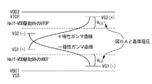
図5Aは、Half−VDD駆動でのデータドライバに供給される電圧同士の関係を示す模式図である。詳しくは後述するが、電源(VSS、VBOT、VTOP、VDD2)及びガンマ(γ)電圧(VG1(−)、VG2(−)、VG1(+)、VG2(+))の電圧関係は、図の上方向に行くに従って高くなる。以降の図も同様である。図6Aは、正極性及び負極性のガンマ曲線がクロスする場合のHalf−VDD駆動でのデータドライバに供給される電圧同士の大小関係を示す模式図である。また、図7Aは、正極性及び負極性のガンマ曲線がクロスしない場合のHalf−VDD駆動でのデータドライバに供給される電圧同士の大小関係を示す模式図である。図8Aは、Half−VDD駆動でのデータドライバに供給される電圧同士の関係を示す模式図である。
どちらの場合も、正極アンプ10に供給される電圧源の電位差は(VDD2−VBOT)であり、負極アンプ20に供給される電圧源の電位差は(VTOP−VSS)であり、Half−VDD動作となっていることが分かる。
VDD2>VTOP>VBOT>VSS (1A)
又は
VDD2>VTOP≒VBOT>VSS (1B)
である。また、正極参照電圧発生回路12に供給されるガンマ電圧VG2(+)、VG1(+)、正極アンプ10に供給される高位電圧源VDD2、低位電圧源VBOTの大小関係は、
VDD2>VG2(+)>VG1(+)>VBOT (2)
である。更に、負極参照電圧発生回路22に供給されるガンマ電圧VG2(−)、VG1(−)、負極アンプ20に供給される高位電圧源VTOP、低位電圧源VSSの大小関係は、
VTOP>VG2(−)>VG1(−)>VSS (3)
である。また更に、ガンマ電圧VG2(+)、基準電圧VRM+、高位電圧源VTOPの大小関係は、
VG2(+)>VRM+>VTOP (4)
であり、低位電圧源VBOT、基準電圧VRM−、ガンマ電圧VG1(−)の大小関係は、
VBOT>VRM−>VG1(−) (5)
である。
一方、図5Bは、Full−VDD駆動でのデータドライバに供給される電圧同士の関係を示す模式図である。図6Bは、正極性及び負極性のガンマ曲線がクロスする場合のFull−VDD駆動でのデータドライバに供給される電圧同士の大小関係を示す模式図である。また、図7Bは、正極性及び負極性のガンマ曲線がクロスしない場合のFull−VDD駆動でのデータドライバに供給される電圧同士の大小関係を示す模式図である。図8Bは、Full−VDD駆動でのデータドライバに供給される電圧同士の関係を示す模式図である。
VDD2≒VTOP>VBOT≒VSS (1C)
である。また、正極参照電圧発生回路12に供給されるガンマ電圧VG2(+)、VG1(+)、正極アンプ10に供給される高位電圧源VDD2、低位電圧源VBOTの大小関係は、上記の式(2)と同じである。更に、負極参照電圧発生回路22に供給されるガンマ電圧VG2(−)、VG1(−)、負極アンプ20に供給される高位電圧源VTOP、低位電圧源VSSの大小関係は、上記の式(3)と同じである。
また更に、ガンマ電圧VG2(+)、基準電圧VRM+、高位電圧源VTOPの大小関係は、
VRM+<VG2(+)<VTOP (6)
であり、低位電圧源VBOT、基準電圧VRM−、ガンマ電圧VG1(−)の大小関係は、
VBOT<VG1(−)<VRM− (7)
である。
例えば、基準電圧VRM+として、第1の映像データD1のデコードで参照される正極参照電圧VR+や、デコードされた第1の映像データの電圧であっても良い。同様に、基準電圧VRM−として、第2の映像データD2のデコードで参照される負極参照電圧VR−や、デコードされた第2の映像データの電圧であっても良い。
上記の各例に示される判定用の基準となる電圧は、上記式(4)及び/又は式(5)を満足することを条件として選択されている。すなわち、そのような条件を必ず有していれば、判定用の基準電圧として、他の回路の他の電圧を用いてもよい。
なお、図7Aの様に、ガンマ曲線がクロスしない場合、VG1(+)>VTOP、VBOT>VG2(−)であることが分かっていれば、判定部40は、判定用に、正極参照電圧発生回路12より選定された基準電圧VRM+として+極性のコモン側γ端子(例示:VG1(+))、及び/又は、負極参照電圧発生回路22より選定された基準電圧VRM−として−極性のコモン側γ端子(VG2(−))をそれぞれ用いてもよいことは明らかである。
図4、図8A、及び図9を参照して、Half−VDD動作時では、電源電圧VBOTとして負極参照電圧発生回路22から選定された基準電圧VRM−より高い電圧が、また、電源電圧VTOPとして正極参照電圧発生回路12から選定された基準電圧VRM+より低い電圧がそれぞれ与えられる。例えば、以下の条件である。
VBOT>基準電圧VRM−
VTOP<基準電圧VRM+
この場合、判定部40はHalf−VDD動作を示す判定信号41(ハイレベルの電圧)を出力する。
図4、図8B、及び図9を参照して、Full−VDD動作時では、電源電圧VBOTとして負極参照電圧発生回路22から選定された基準電圧VRM−より低い電圧が、また、電源電圧VTOPとして正極参照電圧発生回路12から選定された基準電圧VRM+より高い電圧がそれぞれ与えられる。例えば、以下の条件である。
VBOT≒VSS <基準電圧VRM−
VTOP=VDD2>基準電圧VRM+
この場合、判定部40はFull−VDD動作を示す判定信号41(ローレベルの電圧)を出力する。
また、上記液晶表示用ドライバを液晶表示装置に用いることで、上記効果を得ることができると共に、Half−VDD動作及びFull−VDD動作の検出や切換のための他の回路等が不要になり、液晶表示装置の設計が容易化されると共に、液晶表示装置を小型化することができる。
10A 差動部(差動入力段)
10B 中間段
10C 出力段
11 正極デコーダ
20 負極アンプ
20A 差動部(差動入力段)
20B 中間段
20C 出力段
21 負極デコーダ
30 出力スイッチ回路
35 参照電圧発生回路
40 判定部
41 判定信号
81 ラッチアドレスセレクタ
82 ラッチ
83 レベルシフタ
90 液晶表示装置
91 ゲート線
92 データ線
93 トランジスタ
94 画素容量
95 表示コントローラ
96 液晶パネル
97 ゲートドライバ
98 データドライバ
99 画素
110 正極アンプ
111 正極デコーダ
112 正極参照電圧発生回路
120 負極アンプ
121 負極デコーダ
122 負極参照電圧発生回路
130 出力スイッチ回路
Claims (7)
- データ線側の液晶表示用ドライバであって、
第1電源電圧及び前記第1電源電圧より小さい第2電源電圧が供給され、前記デコードされた第1映像データを増幅して第1データ信号として出力する正極アンプと、
第3電源電圧及び前記第3電源電圧より大きい第4電源電圧が供給され、前記デコードされた第2映像データを増幅して第2データ信号として出力する負極アンプと、
前記第2電源電圧と第1基準電圧との比較結果、又は、前記第4電源電圧と第2基準電圧との比較結果に基づいて、Half−VDD動作及びFull−VDD動作のいずれかであるかを判定し、判定結果を示す判定信号を出力する判定部と
を具備し、
前記正極アンプ及び前記負極アンプは、前記判定信号に基づいて、Half−VDD動作及びFull−VDD動作のうちのいずれか一方により前記増幅を行う
液晶表示用ドライバ。 - 請求項1に記載の液晶表示用ドライバにおいて、
前記第1基準電圧は、負極性γ電圧、前記第2映像データのデコードで参照される負極参照電圧、又は、前記デコードされた第2映像データの電圧のいずれかであり、
前記第2基準電圧は、正極性γ電圧、前記第1映像データデコードで参照される正極参照電圧、又は、前記デコードされた第1映像データの電圧のいずれかである
液晶表示用ドライバ。 - 請求項1又は2に記載の液晶表示用ドライバにおいて、
前記判定部は、前記第2電源電圧が、前記第1基準電圧よりも大きい、又は、前記第4電源電圧が、前記第2基準電圧よりも小さい場合、前記Half−VDD動作であると判定し、
前記正極アンプ及び前記負極アンプは、前記Half−VDD動作する
液晶表示用ドライバ。 - 請求項3に記載の液晶表示用ドライバにおいて、
前記判定部は、前記第2電源電圧が、前記第1基準電圧よりも小さい、又は、前記第4電源電圧が、前記第2基準電圧よりも大きい場合、前記Full−VDD動作であると判定し、
前記正極アンプ及び前記負極アンプは、前記Full−VDD動作する
液晶表示用ドライバ。 - 請求項1乃至4のいずれか一項に記載の液晶表示用ドライバにおいて、
複数の正極性γ電圧に基づいて、複数の正極参照電圧を生成する正極参照電圧発生回路と、
第1映像データに基づいて、前記複数の正極参照電圧から少なくとも一つの正極参照電圧をデコードされた第1映像データとして選択する正極デコーダと、
複数の負極性γ電圧に基づいて、複数の負極参照電圧を生成する負極参照電圧発生回路と、
第2映像データに基づいて、前記複数の負極参照電圧から少なくとも一つの負極参照電圧をデコードされた第2映像データとして選択する負極デコーダと、
を更に具備する
液晶表示用ドライバ。 - 請求項5に記載の液晶表示用ドライバにおいて、
前記正極アンプは、
前記第1電源電圧と前記第3電源電圧とを供給され、前記デコードされた第1映像データと前記第1データ信号とを差動増幅する第1差動段と、
前記第1電源電圧と前記第2電源電圧とを供給され、前記第1差動段による差動増幅出力をAB級増幅する第1出力段と、
前記第1電源電圧と前記第2電源電圧とを供給され、前記第1出力段によるAB級増幅出力の波形歪みを補正する第1中間段と
を備え、
前記第1中間段は、前記判定信号に基づいて、前記第1出力段へ供給する電圧を調整し、
前記負極アンプは、
前記第3電源電圧と前記第1電源電圧とを供給され、前記デコードされた第2映像データと前記第2データ信号とを差動増幅する第2差動段と、
前記第3電源電圧と前記第4電源電圧とを供給され、前記第2差動段による差動増幅出力をAB級増幅する第2出力段と、
前記第3電源電圧と前記第4電源電圧とを供給され、前記第2出力段によるAB級増幅出力の波形歪みを補正する第2中間段と
を備え、
前記第2中間段は、前記判定信号に基づいて、前記第2出力段へ供給する電圧を調整する
液晶表示用ドライバ。 - 液晶パネルと、
前記液晶表示パネルを駆動する請求項1乃至6のいずれか一項に記載の液晶表示用ドライバと
を具備する
液晶表示装置。
Priority Applications (3)
| Application Number | Priority Date | Filing Date | Title |
|---|---|---|---|
| JP2010059471A JP5241036B2 (ja) | 2009-07-07 | 2010-03-16 | 液晶表示用ドライバ及び液晶表示装置 |
| US12/826,121 US20110007057A1 (en) | 2009-07-07 | 2010-06-29 | Liquid crystal display driver and liquid crystal display device |
| CN2010102212317A CN101944341A (zh) | 2009-07-07 | 2010-06-30 | 液晶显示驱动器和液晶显示装置 |
Applications Claiming Priority (3)
| Application Number | Priority Date | Filing Date | Title |
|---|---|---|---|
| JP2009161115 | 2009-07-07 | ||
| JP2009161115 | 2009-07-07 | ||
| JP2010059471A JP5241036B2 (ja) | 2009-07-07 | 2010-03-16 | 液晶表示用ドライバ及び液晶表示装置 |
Publications (2)
| Publication Number | Publication Date |
|---|---|
| JP2011034051A JP2011034051A (ja) | 2011-02-17 |
| JP5241036B2 true JP5241036B2 (ja) | 2013-07-17 |
Family
ID=43427106
Family Applications (1)
| Application Number | Title | Priority Date | Filing Date |
|---|---|---|---|
| JP2010059471A Expired - Fee Related JP5241036B2 (ja) | 2009-07-07 | 2010-03-16 | 液晶表示用ドライバ及び液晶表示装置 |
Country Status (3)
| Country | Link |
|---|---|
| US (1) | US20110007057A1 (ja) |
| JP (1) | JP5241036B2 (ja) |
| CN (1) | CN101944341A (ja) |
Families Citing this family (8)
| Publication number | Priority date | Publication date | Assignee | Title |
|---|---|---|---|---|
| TW201342339A (zh) * | 2012-04-10 | 2013-10-16 | Wintek Corp | 可調整輸出伽瑪參考電壓的方法和可調整輸出伽瑪參考電壓的源極驅動電路 |
| US9099026B2 (en) | 2012-09-27 | 2015-08-04 | Lapis Semiconductor Co., Ltd. | Source driver IC chip |
| US20140176519A1 (en) * | 2012-12-25 | 2014-06-26 | Shenzhen China Star Optoelectronics Technology Co. Ltd. | Programmable Gamma Circuit of Liquid Crystal Display Driving System |
| TW201516997A (zh) * | 2013-10-29 | 2015-05-01 | Novatek Microelectronics Corp | 源極驅動器及其驅動方法 |
| CN104616613B (zh) * | 2013-11-04 | 2018-05-18 | 联咏科技股份有限公司 | 源极驱动器及其驱动方法 |
| JP2015090414A (ja) * | 2013-11-06 | 2015-05-11 | シナプティクス・ディスプレイ・デバイス株式会社 | 表示駆動回路および表示装置 |
| CN107680547B (zh) * | 2014-02-13 | 2021-04-13 | 联咏科技股份有限公司 | 缓冲电路、面板模块及显示驱动方法 |
| US10083668B2 (en) * | 2016-03-09 | 2018-09-25 | Semiconductor Energy Laboratory Co., Ltd. | Semiconductor device, display device, and electronic device |
Family Cites Families (11)
| Publication number | Priority date | Publication date | Assignee | Title |
|---|---|---|---|---|
| TW277129B (ja) * | 1993-12-24 | 1996-06-01 | Sharp Kk | |
| JP3056085B2 (ja) * | 1996-08-20 | 2000-06-26 | 日本電気株式会社 | マトリクス型液晶表示装置の駆動回路 |
| US6628274B1 (en) * | 1999-03-26 | 2003-09-30 | Seiko Epson Corporation | Display drive device, display device, hand-carry electronic device, and display driving method |
| JP4744686B2 (ja) * | 2000-12-06 | 2011-08-10 | ルネサスエレクトロニクス株式会社 | 演算増幅器 |
| JP4172471B2 (ja) * | 2005-06-17 | 2008-10-29 | セイコーエプソン株式会社 | 駆動回路、電気光学装置及び電子機器 |
| KR20070056779A (ko) * | 2005-11-30 | 2007-06-04 | 삼성전자주식회사 | 데이터 구동 집적회로장치와 이를 포함하는 액정표시장치 |
| JP4275166B2 (ja) * | 2006-11-02 | 2009-06-10 | Necエレクトロニクス株式会社 | データドライバ及び表示装置 |
| JP2009168841A (ja) * | 2008-01-10 | 2009-07-30 | Nec Electronics Corp | 演算増幅器及び駆動回路、液晶表示装置の駆動方法 |
| JP2009194485A (ja) * | 2008-02-12 | 2009-08-27 | Nec Electronics Corp | 演算増幅器回路、及び表示装置 |
| JP4526581B2 (ja) * | 2008-08-06 | 2010-08-18 | ルネサスエレクトロニクス株式会社 | 液晶表示パネル駆動用ドライバ、及び液晶表示装置 |
| US8154503B2 (en) * | 2009-09-01 | 2012-04-10 | Au Optronics Corporation | Method and apparatus for driving a liquid crystal display device |
-
2010
- 2010-03-16 JP JP2010059471A patent/JP5241036B2/ja not_active Expired - Fee Related
- 2010-06-29 US US12/826,121 patent/US20110007057A1/en not_active Abandoned
- 2010-06-30 CN CN2010102212317A patent/CN101944341A/zh active Pending
Also Published As
| Publication number | Publication date |
|---|---|
| JP2011034051A (ja) | 2011-02-17 |
| US20110007057A1 (en) | 2011-01-13 |
| CN101944341A (zh) | 2011-01-12 |
Similar Documents
| Publication | Publication Date | Title |
|---|---|---|
| JP5241036B2 (ja) | 液晶表示用ドライバ及び液晶表示装置 | |
| JP4275166B2 (ja) | データドライバ及び表示装置 | |
| US8390609B2 (en) | Differential amplifier and drive circuit of display device using the same | |
| US8217925B2 (en) | Display panel driver and display device | |
| JP4825838B2 (ja) | 出力増幅回路及びそれを用いた表示装置のデータドライバ | |
| US10650770B2 (en) | Output circuit and data driver of liquid crystal display device | |
| JP4840908B2 (ja) | 表示装置駆動回路 | |
| US7903078B2 (en) | Data driver and display device | |
| US20090040165A1 (en) | Amplifying circuit and display unit | |
| US20070290979A1 (en) | Source drive amplifier for flat panel display | |
| US20120019502A1 (en) | Source driver for a liquid crystal display device and liquid crystal display device using the same | |
| JP5442558B2 (ja) | 出力回路及びデータドライバ及び表示装置 | |
| JP2013085080A (ja) | 出力回路及びデータドライバ及び表示装置 | |
| JP2008152076A (ja) | 液晶表示装置、ソースドライバ及び液晶表示パネル駆動方法 | |
| JP2011138008A (ja) | 駆動回路及び表示装置 | |
| JP2008134496A (ja) | 階調電位発生回路、表示装置のデータドライバ、及びその表示装置 | |
| JP5236434B2 (ja) | 表示パネルの駆動電圧出力回路 | |
| JP5236435B2 (ja) | 表示パネルの駆動電圧出力回路 | |
| TWI406249B (zh) | 液晶點反轉驅動電路 | |
| JP2012137571A (ja) | 液晶表示装置用ソースアンプ、ソースドライバ及び液晶表示装置 | |
| JP4846819B2 (ja) | データドライバ及び表示装置 | |
| JP2011053623A (ja) | 液晶パネルの駆動回路及び表示装置 | |
| JP5650297B2 (ja) | 駆動回路及び表示装置 | |
| JP2013068915A (ja) | 液晶表示装置の駆動装置 |
Legal Events
| Date | Code | Title | Description |
|---|---|---|---|
| A621 | Written request for application examination |
Free format text: JAPANESE INTERMEDIATE CODE: A621 Effective date: 20120720 |
|
| A977 | Report on retrieval |
Free format text: JAPANESE INTERMEDIATE CODE: A971007 Effective date: 20130220 |
|
| TRDD | Decision of grant or rejection written | ||
| A01 | Written decision to grant a patent or to grant a registration (utility model) |
Free format text: JAPANESE INTERMEDIATE CODE: A01 Effective date: 20130327 |
|
| A61 | First payment of annual fees (during grant procedure) |
Free format text: JAPANESE INTERMEDIATE CODE: A61 Effective date: 20130401 |
|
| FPAY | Renewal fee payment (event date is renewal date of database) |
Free format text: PAYMENT UNTIL: 20160412 Year of fee payment: 3 |
|
| R150 | Certificate of patent or registration of utility model |
Free format text: JAPANESE INTERMEDIATE CODE: R150 |
|
| S531 | Written request for registration of change of domicile |
Free format text: JAPANESE INTERMEDIATE CODE: R313531 |
|
| R350 | Written notification of registration of transfer |
Free format text: JAPANESE INTERMEDIATE CODE: R350 |
|
| LAPS | Cancellation because of no payment of annual fees |