JP5220522B2 - 発光装置、発光モジュール - Google Patents
発光装置、発光モジュール Download PDFInfo
- Publication number
- JP5220522B2 JP5220522B2 JP2008231353A JP2008231353A JP5220522B2 JP 5220522 B2 JP5220522 B2 JP 5220522B2 JP 2008231353 A JP2008231353 A JP 2008231353A JP 2008231353 A JP2008231353 A JP 2008231353A JP 5220522 B2 JP5220522 B2 JP 5220522B2
- Authority
- JP
- Japan
- Prior art keywords
- light
- light emitting
- resin
- emitting device
- emitting element
- Prior art date
- Legal status (The legal status is an assumption and is not a legal conclusion. Google has not performed a legal analysis and makes no representation as to the accuracy of the status listed.)
- Expired - Fee Related
Links
Images


Classifications
-
- H—ELECTRICITY
- H10—SEMICONDUCTOR DEVICES; ELECTRIC SOLID-STATE DEVICES NOT OTHERWISE PROVIDED FOR
- H10W—GENERIC PACKAGES, INTERCONNECTIONS, CONNECTORS OR OTHER CONSTRUCTIONAL DETAILS OF DEVICES COVERED BY CLASS H10
- H10W72/00—Interconnections or connectors in packages
- H10W72/50—Bond wires
- H10W72/551—Materials of bond wires
- H10W72/552—Materials of bond wires comprising metals or metalloids, e.g. silver
- H10W72/5522—Materials of bond wires comprising metals or metalloids, e.g. silver comprising gold [Au]
-
- H—ELECTRICITY
- H10—SEMICONDUCTOR DEVICES; ELECTRIC SOLID-STATE DEVICES NOT OTHERWISE PROVIDED FOR
- H10W—GENERIC PACKAGES, INTERCONNECTIONS, CONNECTORS OR OTHER CONSTRUCTIONAL DETAILS OF DEVICES COVERED BY CLASS H10
- H10W90/00—Package configurations
- H10W90/701—Package configurations characterised by the relative positions of pads or connectors relative to package parts
- H10W90/751—Package configurations characterised by the relative positions of pads or connectors relative to package parts of bond wires
- H10W90/756—Package configurations characterised by the relative positions of pads or connectors relative to package parts of bond wires between a chip and a stacked lead frame, conducting package substrate or heat sink
Landscapes
- Led Device Packages (AREA)
Description
さらに、導体部における銀メッキ層の光沢度が、0.5以上且つ0.7以下であることを特徴とすることができる。
さらにまた、封止樹脂が、シリコン樹脂にて構成されることを特徴とすることができる。
さらに、導体部における銀メッキ層の光沢度が、0.5以上且つ0.7以下であることを特徴とすることができる。
さらにまた、可視領域における樹脂容器および導体部の銀メッキ層の光反射率が85%以上98%以下であることを特徴とすることができる。
そして、凹部の底面に露出する導体部の面積が、底面の全面積の半分以上に設定されることを特徴とすることができる。
さらに、発光装置の導体部における銀メッキ層の光沢度が、0.5以上且つ0.7以下であることを特徴とすることができる。
<実施の形態1>
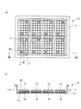
図1は、本実施の形態が適用される液晶表示装置の全体構成を示す図である。この液晶表示装置は、液晶表示モジュール50と、この液晶表示モジュール50の背面側(図1では下部側)に設けられるバックライト装置10とを備えている。
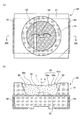
この半導体発光素子64は、n型電極およびp型電極を有しており、ボンディングワイヤを介して、p型電極がアノード用リード部62に、n型電極がカソード用リード部63に、それぞれ接続されている。なお、本実施の形態で用いた発光装置60では、図3(a)に示すように、半導体発光素子64が、円形状を有する底面70のほぼ中央部に取り付けられている。
この発光装置60においては、図3(b)に示すように、出射面65cの中央部が樹脂容器61の上面よりも凹んでおり、その凹み量dが上面から−20μm〜−100μmの範囲に設定されている。凹み量dは、樹脂容器61の開口端の高さと、出射面65cの最低高さとの差になる。なお、ここでは、樹脂容器61の開口端の高さを基準(0)としたとき、半導体発光素子64に近づく側をマイナス(−)としている。したがって、凹み量dが上面から−20μm〜−100μmの範囲とは、樹脂容器61の開口端の高さを0μmとしたときに、出射面65cの最低高さが上面よりも20μm〜100μmの範囲で半導体発光素子64側に位置していることを意味する。
アノード用リード部62を正極とし、カソード用リード部63を負極として半導体発光素子64に電流を流すと、半導体発光素子64は青色光を出力する。半導体発光素子64から出力された青色光は、封止樹脂65内を進行し、直接あるいは底面70や壁面80で反射した後に出射面65cから外部に出射される。但し、出射面65cに向かう光の一部は、出射面65cで反射し、再び封止樹脂65内を進行する。この間、封止樹脂65内において、青色光の一部は蛍光体粉体65aによって緑色光および赤色光に変換され、変換された緑色光および赤色光は、直接あるいは底面70や壁面80で反射した後、青色光と共に出射面65cから外部に出射される。したがって、出射面65cからは、青色光、緑色光および赤色光を含む白色光が出射されることになる。
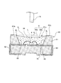
まず、アノード用リード部62およびカソード用リード部63を一体化したリードフレームに、白色樹脂を射出成形して、凹部61aを有する樹脂容器61を形成する。次いで、樹脂容器61の凹部61aの底面70に露出するカソード用リード部63上に半導体発光素子64を接着固定し、ボンディングワイヤによって半導体発光素子64のp型電極、n型電極と、アノード用リード部62、カソード用リード部63とを、それぞれ接続する。
図5は、本実施の形態が適用される発光装置60の構成を説明するための図である。ここで、図5(a)は発光装置60の上面図を、図5(b)は図5(a)のVB−VB断面図を、それぞれ示している。
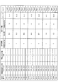
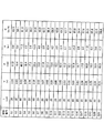
図6は、実施例および比較例に用いた各試料とその構成との関係を示す図である。
この実験では、寸法の異なる3種類の樹脂容器61を用意した。ここで第1の樹脂容器61(Type1と呼ぶ)は、上面における縦横の大きさが3.5mm×2.8mmであり、第2の樹脂容器61(Type2)は、上面における縦横の大きさが3.8mm×0.8mmであり、第3の筐体(Type3)は上面における縦横の大きさが5.0mm×5.5mmである。また、Type1〜Type3の樹脂容器61を構成する白色樹脂の可視領域における光吸収率は7%である。なお、Type1およびType2の樹脂容器61を有する発光装置60は、図3に示した構造を有しており、それぞれには1個の半導体発光素子64が搭載されている。一方、Type3の樹脂容器61を有する発光装置60は、図5に示した構造を有しており、3個の半導体発光素子64(第1半導体発光素子64a、第2半導体発光素子64b、第3半導体発光素子64c)が搭載されている。
Type1およびType2の樹脂容器61を有する試料S1、S2、S4、S5、S7、S8、S10、S11、S13、S14、S16、S17、S19、S20は、1枚のリードフレームに対し、白色樹脂にて144個の樹脂容器61を形成して作成した。一方、Type3の筐体を有する試料S3、S6、S9、S12、S15、S18、S21は、1枚のリードフレームに対し、白色樹脂にて40個の樹脂容器61を形成して作成した。なお、試料S1〜S21のそれぞれにおいて、樹脂容器61の凹部61aの深さはすべて0.6mmである。
Claims (12)
- 凹部を有する樹脂容器と、
金属導体と、当該金属導体の表面に形成された0.3以上且つ1.0以下の光沢度(JISZ8741:入射角=60°)を有する銀メッキ層とを有し、前記樹脂容器の前記凹部の内側に露出した状態で配置される導体部と、
前記凹部の内側に設けられ、前記導体部と電気的に接続される発光素子と、
前記発光素子から出力される光に対する透光性を有し、前記凹部において当該発光素子を封止する封止樹脂と
を含む発光装置。 - 前記樹脂容器は、白色顔料を用いて白色化されており、前記凹部において露出する当該樹脂容器および前記銀メッキ層の、可視領域における光吸収率が12%未満であることを特徴とする請求項1記載の発光装置。
- 前記導体部における前記銀メッキ層の光沢度が、0.5以上且つ0.7以下であることを特徴とする請求項1または2記載の発光装置。
- 前記封止樹脂が、シリコン樹脂にて構成されることを特徴とする請求項1ないし3のいずれか1項記載の発光装置。
- 底面と、当該底面の周縁から立ち上がる壁面とを含む凹部を備えた樹脂容器と、
金属導体と、当該金属導体の表面に形成された0.3以上且つ1.0以下の光沢度(JISZ8741:入射角=60°)を有する銀メッキ層とを有し、前記樹脂容器の前記凹部の前記底面に露出した状態で配置される導体部と、
前記凹部の前記底面に取り付けられ、前記導体部と電気的に接続される発光素子と、
前記発光素子から出力される光に対する透光性を有し、前記凹部において当該発光素子を封止する封止樹脂と
を含む発光装置。 - 前記樹脂容器が、チタニア微粒子を含む樹脂にて構成され、前記凹部において露出する当該樹脂容器および前記銀メッキ層の、可視領域における光吸収率が12%未満であることを特徴とする請求項5記載の発光装置。
- 前記導体部における前記銀メッキ層の光沢度が、0.5以上且つ0.7以下であることを特徴とする請求項5または6記載の発光装置。
- 可視領域における前記樹脂容器および前記導体部の前記銀メッキ層の光反射率が85%以上98%以下であることを特徴とする請求項5ないし7のいずれか1項記載の発光装置。
- 前記凹部の前記底面に露出する前記導体部の面積が、当該底面の全面積の半分以上に設定されることを特徴とする請求項5ないし8のいずれか1項記載の発光装置。
- 基板と、
前記基板に取り付けられる複数の発光装置とを備え、
前記発光装置は、
凹部を有する樹脂容器と、
金属導体と、当該金属導体の表面に形成された0.3以上且つ1.0以下の光沢度(JISZ8741:入射角=60°)を有する銀メッキ層とを有し、前記樹脂容器の前記凹部の内側に露出した状態で配置される導体部と、
前記凹部の内側に設けられ、前記導体部と電気的に接続される発光素子と、
前記発光素子から出力される光に対する透光性を有し、前記凹部において当該発光素子を封止する封止樹脂と
を有することを特徴とする発光モジュール。 - 前記発光装置の前記樹脂容器は、白色顔料を用いて白色化されており、前記凹部において露出する当該樹脂容器および前記銀メッキ層の、可視領域における光吸収率が12%未満であることを特徴とする請求項10記載の発光モジュール。
- 前記発光装置の前記導体部における前記銀メッキ層の光沢度が、0.5以上且つ0.7以下であることを特徴とする請求項10または11記載の発光モジュール。
Priority Applications (4)
| Application Number | Priority Date | Filing Date | Title |
|---|---|---|---|
| JP2008231353A JP5220522B2 (ja) | 2008-09-09 | 2008-09-09 | 発光装置、発光モジュール |
| US13/062,152 US8378369B2 (en) | 2008-09-09 | 2009-09-01 | Light emitting unit, light emitting module, and display device |
| PCT/JP2009/065247 WO2010029872A1 (ja) | 2008-09-09 | 2009-09-01 | 発光装置、発光モジュール、表示装置 |
| TW098130222A TWI425655B (zh) | 2008-09-09 | 2009-09-08 | A light emitting device, a light emitting module, and a display device |
Applications Claiming Priority (1)
| Application Number | Priority Date | Filing Date | Title |
|---|---|---|---|
| JP2008231353A JP5220522B2 (ja) | 2008-09-09 | 2008-09-09 | 発光装置、発光モジュール |
Publications (2)
| Publication Number | Publication Date |
|---|---|
| JP2010067720A JP2010067720A (ja) | 2010-03-25 |
| JP5220522B2 true JP5220522B2 (ja) | 2013-06-26 |
Family
ID=42193068
Family Applications (1)
| Application Number | Title | Priority Date | Filing Date |
|---|---|---|---|
| JP2008231353A Expired - Fee Related JP5220522B2 (ja) | 2008-09-09 | 2008-09-09 | 発光装置、発光モジュール |
Country Status (1)
| Country | Link |
|---|---|
| JP (1) | JP5220522B2 (ja) |
Families Citing this family (6)
| Publication number | Priority date | Publication date | Assignee | Title |
|---|---|---|---|---|
| JP6011010B2 (ja) * | 2012-05-01 | 2016-10-19 | 大日本印刷株式会社 | Led用リードフレームまたは基板およびその製造方法、ならびに半導体装置およびその製造方法 |
| JP5998621B2 (ja) * | 2012-05-10 | 2016-09-28 | 大日本印刷株式会社 | Led用リードフレーム及び当該led用リードフレームを用いた半導体装置 |
| CN104685347B (zh) * | 2012-10-04 | 2017-03-22 | 东丽株式会社 | 丝线的检查方法、丝线的检查装置、丝线的制造方法、丝线卷装以及丝线模块 |
| JP6206568B2 (ja) * | 2016-09-01 | 2017-10-04 | 大日本印刷株式会社 | 半導体装置 |
| JP6222318B2 (ja) * | 2016-09-07 | 2017-11-01 | 大日本印刷株式会社 | Led用リードフレームまたは基板およびその製造方法、ならびに半導体装置およびその製造方法 |
| WO2021117267A1 (ja) * | 2019-12-13 | 2021-06-17 | ヌヴォトンテクノロジージャパン株式会社 | 照明パネル及び照明装置 |
Family Cites Families (7)
| Publication number | Priority date | Publication date | Assignee | Title |
|---|---|---|---|---|
| JP3991961B2 (ja) * | 2002-09-05 | 2007-10-17 | 日亜化学工業株式会社 | 側面発光型発光装置 |
| JP5021151B2 (ja) * | 2003-11-19 | 2012-09-05 | 株式会社カネカ | 半導体のパッケージ用硬化性樹脂組成物および半導体 |
| JP4436265B2 (ja) * | 2005-02-16 | 2010-03-24 | 日本特殊陶業株式会社 | 発光素子実装用配線基板 |
| JP4918238B2 (ja) * | 2005-09-13 | 2012-04-18 | 昭和電工株式会社 | 発光装置 |
| CN101461070B (zh) * | 2006-06-02 | 2013-07-24 | 日立化成株式会社 | 光半导体元件搭载用封装及使用其的光半导体装置 |
| JP2008041699A (ja) * | 2006-08-01 | 2008-02-21 | Showa Denko Kk | Ledパッケージ |
| JP2008201828A (ja) * | 2007-02-16 | 2008-09-04 | Nippon Steel Chem Co Ltd | 発光ダイオード |
-
2008
- 2008-09-09 JP JP2008231353A patent/JP5220522B2/ja not_active Expired - Fee Related
Also Published As
| Publication number | Publication date |
|---|---|
| JP2010067720A (ja) | 2010-03-25 |
Similar Documents
| Publication | Publication Date | Title |
|---|---|---|
| WO2010029872A1 (ja) | 発光装置、発光モジュール、表示装置 | |
| JP5220527B2 (ja) | 発光装置、発光モジュール | |
| JP5220526B2 (ja) | 発光装置、発光モジュール、表示装置 | |
| CN1237631C (zh) | Led器件 | |
| CN104040382B (zh) | 光学片以及具有该光学片的显示装置和发光装置 | |
| JP7096512B2 (ja) | 発光装置 | |
| JP2008218460A (ja) | 半導体発光装置 | |
| US11233177B2 (en) | Light emitting device package having lead electrode with varying thickness | |
| JP5220522B2 (ja) | 発光装置、発光モジュール | |
| CN108963056B (zh) | 发光装置 | |
| JP2006253336A (ja) | 光源装置 | |
| KR20120132931A (ko) | 발광소자패키지 | |
| US20190027663A1 (en) | Light emitting device | |
| JP6524624B2 (ja) | 発光装置 | |
| KR20120131712A (ko) | 발광소자 패키지 | |
| JP6326830B2 (ja) | 発光装置及びそれを備える照明装置 | |
| JP2007088060A (ja) | 発光装置 | |
| KR20120045539A (ko) | 발광소자 패키지 | |
| KR20030031061A (ko) | 고효율 색변환 층을 갖는 발광 소자 및 그 제조 방법 | |
| JP2009224376A (ja) | 側面型発光装置及びその製造方法 | |
| KR102019501B1 (ko) | 형광체 및 이를 구비한 발광 소자 | |
| JP2019175892A (ja) | 発光モジュール及びその製造方法 | |
| KR20130117572A (ko) | 발광소자 패키지 및 백라이트 유닛 | |
| KR20130025455A (ko) | 발광소자 패키지 | |
| KR20120073929A (ko) | 발광소자 패키지 |
Legal Events
| Date | Code | Title | Description |
|---|---|---|---|
| A621 | Written request for application examination |
Free format text: JAPANESE INTERMEDIATE CODE: A621 Effective date: 20110601 |
|
| A131 | Notification of reasons for refusal |
Free format text: JAPANESE INTERMEDIATE CODE: A131 Effective date: 20120403 |
|
| A02 | Decision of refusal |
Free format text: JAPANESE INTERMEDIATE CODE: A02 Effective date: 20120918 |
|
| A521 | Request for written amendment filed |
Free format text: JAPANESE INTERMEDIATE CODE: A523 Effective date: 20121204 |
|
| A911 | Transfer to examiner for re-examination before appeal (zenchi) |
Free format text: JAPANESE INTERMEDIATE CODE: A911 Effective date: 20121211 |
|
| TRDD | Decision of grant or rejection written | ||
| A01 | Written decision to grant a patent or to grant a registration (utility model) |
Free format text: JAPANESE INTERMEDIATE CODE: A01 Effective date: 20130219 |
|
| A61 | First payment of annual fees (during grant procedure) |
Free format text: JAPANESE INTERMEDIATE CODE: A61 Effective date: 20130306 |
|
| FPAY | Renewal fee payment (event date is renewal date of database) |
Free format text: PAYMENT UNTIL: 20160315 Year of fee payment: 3 |
|
| R150 | Certificate of patent or registration of utility model |
Ref document number: 5220522 Country of ref document: JP Free format text: JAPANESE INTERMEDIATE CODE: R150 Free format text: JAPANESE INTERMEDIATE CODE: R150 |
|
| R250 | Receipt of annual fees |
Free format text: JAPANESE INTERMEDIATE CODE: R250 |
|
| LAPS | Cancellation because of no payment of annual fees |