JP5211468B2 - 半導体装置の製造方法 - Google Patents
半導体装置の製造方法 Download PDFInfo
- Publication number
- JP5211468B2 JP5211468B2 JP2006316807A JP2006316807A JP5211468B2 JP 5211468 B2 JP5211468 B2 JP 5211468B2 JP 2006316807 A JP2006316807 A JP 2006316807A JP 2006316807 A JP2006316807 A JP 2006316807A JP 5211468 B2 JP5211468 B2 JP 5211468B2
- Authority
- JP
- Japan
- Prior art keywords
- region
- semiconductor device
- mask material
- semiconductor
- manufacturing
- Prior art date
- Legal status (The legal status is an assumption and is not a legal conclusion. Google has not performed a legal analysis and makes no representation as to the accuracy of the status listed.)
- Active
Links
- 239000004065 semiconductor Substances 0.000 title claims description 409
- 238000004519 manufacturing process Methods 0.000 title claims description 110
- 239000000463 material Substances 0.000 claims description 158
- 125000005842 heteroatom Chemical group 0.000 claims description 129
- 230000005684 electric field Effects 0.000 claims description 101
- 238000000034 method Methods 0.000 claims description 85
- 239000012535 impurity Substances 0.000 claims description 62
- 239000000758 substrate Substances 0.000 claims description 57
- 229910021420 polycrystalline silicon Inorganic materials 0.000 claims description 27
- HBMJWWWQQXIZIP-UHFFFAOYSA-N silicon carbide Chemical compound [Si+]#[C-] HBMJWWWQQXIZIP-UHFFFAOYSA-N 0.000 claims description 25
- 229910010271 silicon carbide Inorganic materials 0.000 claims description 25
- 230000003647 oxidation Effects 0.000 claims description 24
- 238000007254 oxidation reaction Methods 0.000 claims description 24
- 238000005468 ion implantation Methods 0.000 claims description 16
- 238000010438 heat treatment Methods 0.000 claims description 7
- 229910021421 monocrystalline silicon Inorganic materials 0.000 claims description 4
- 230000003213 activating effect Effects 0.000 claims description 3
- 229910002601 GaN Inorganic materials 0.000 claims description 2
- JMASRVWKEDWRBT-UHFFFAOYSA-N Gallium nitride Chemical compound [Ga]#N JMASRVWKEDWRBT-UHFFFAOYSA-N 0.000 claims description 2
- 229910021417 amorphous silicon Inorganic materials 0.000 claims description 2
- 229910003460 diamond Inorganic materials 0.000 claims description 2
- 239000010432 diamond Substances 0.000 claims description 2
- KRHYYFGTRYWZRS-UHFFFAOYSA-N Fluorane Chemical compound F KRHYYFGTRYWZRS-UHFFFAOYSA-N 0.000 description 30
- 239000010410 layer Substances 0.000 description 21
- 239000011259 mixed solution Substances 0.000 description 21
- 238000005530 etching Methods 0.000 description 18
- 238000001039 wet etching Methods 0.000 description 16
- DDFHBQSCUXNBSA-UHFFFAOYSA-N 5-(5-carboxythiophen-2-yl)thiophene-2-carboxylic acid Chemical compound S1C(C(=O)O)=CC=C1C1=CC=C(C(O)=O)S1 DDFHBQSCUXNBSA-UHFFFAOYSA-N 0.000 description 15
- MHAJPDPJQMAIIY-UHFFFAOYSA-N Hydrogen peroxide Chemical compound OO MHAJPDPJQMAIIY-UHFFFAOYSA-N 0.000 description 12
- QAOWNCQODCNURD-UHFFFAOYSA-N Sulfuric acid Chemical compound OS(O)(=O)=O QAOWNCQODCNURD-UHFFFAOYSA-N 0.000 description 12
- 229910052782 aluminium Inorganic materials 0.000 description 12
- XAGFODPZIPBFFR-UHFFFAOYSA-N aluminium Chemical compound [Al] XAGFODPZIPBFFR-UHFFFAOYSA-N 0.000 description 12
- 238000001312 dry etching Methods 0.000 description 12
- 239000010936 titanium Substances 0.000 description 12
- 230000000694 effects Effects 0.000 description 11
- 239000011229 interlayer Substances 0.000 description 10
- ZOXJGFHDIHLPTG-UHFFFAOYSA-N Boron Chemical compound [B] ZOXJGFHDIHLPTG-UHFFFAOYSA-N 0.000 description 9
- PXHVJJICTQNCMI-UHFFFAOYSA-N Nickel Chemical compound [Ni] PXHVJJICTQNCMI-UHFFFAOYSA-N 0.000 description 9
- 230000004888 barrier function Effects 0.000 description 9
- 229910052796 boron Inorganic materials 0.000 description 9
- 230000008569 process Effects 0.000 description 8
- 239000002772 conduction electron Substances 0.000 description 7
- VYPSYNLAJGMNEJ-UHFFFAOYSA-N Silicium dioxide Chemical compound O=[Si]=O VYPSYNLAJGMNEJ-UHFFFAOYSA-N 0.000 description 6
- RTAQQCXQSZGOHL-UHFFFAOYSA-N Titanium Chemical compound [Ti] RTAQQCXQSZGOHL-UHFFFAOYSA-N 0.000 description 6
- 229910052785 arsenic Inorganic materials 0.000 description 6
- RQNWIZPPADIBDY-UHFFFAOYSA-N arsenic atom Chemical compound [As] RQNWIZPPADIBDY-UHFFFAOYSA-N 0.000 description 6
- 238000005229 chemical vapour deposition Methods 0.000 description 6
- 229910052814 silicon oxide Inorganic materials 0.000 description 6
- 229910052719 titanium Inorganic materials 0.000 description 6
- OAICVXFJPJFONN-UHFFFAOYSA-N Phosphorus Chemical compound [P] OAICVXFJPJFONN-UHFFFAOYSA-N 0.000 description 5
- 230000004913 activation Effects 0.000 description 5
- 229910052698 phosphorus Inorganic materials 0.000 description 5
- 239000011574 phosphorus Substances 0.000 description 5
- 239000002344 surface layer Substances 0.000 description 5
- 238000009826 distribution Methods 0.000 description 4
- 150000002500 ions Chemical class 0.000 description 4
- 238000001020 plasma etching Methods 0.000 description 4
- 238000009792 diffusion process Methods 0.000 description 3
- 230000005669 field effect Effects 0.000 description 3
- 229910052759 nickel Inorganic materials 0.000 description 3
- 230000001603 reducing effect Effects 0.000 description 3
- 238000000137 annealing Methods 0.000 description 2
- 238000000151 deposition Methods 0.000 description 2
- 238000005566 electron beam evaporation Methods 0.000 description 2
- 238000001017 electron-beam sputter deposition Methods 0.000 description 2
- 238000005224 laser annealing Methods 0.000 description 2
- 238000001451 molecular beam epitaxy Methods 0.000 description 2
- 229910052757 nitrogen Inorganic materials 0.000 description 2
- 238000000059 patterning Methods 0.000 description 2
- 238000000206 photolithography Methods 0.000 description 2
- 230000009467 reduction Effects 0.000 description 2
- 239000007790 solid phase Substances 0.000 description 2
- 229910052720 vanadium Inorganic materials 0.000 description 2
- LEONUFNNVUYDNQ-UHFFFAOYSA-N vanadium atom Chemical compound [V] LEONUFNNVUYDNQ-UHFFFAOYSA-N 0.000 description 2
- 229910000577 Silicon-germanium Inorganic materials 0.000 description 1
- LEVVHYCKPQWKOP-UHFFFAOYSA-N [Si].[Ge] Chemical compound [Si].[Ge] LEVVHYCKPQWKOP-UHFFFAOYSA-N 0.000 description 1
- 238000009825 accumulation Methods 0.000 description 1
- 230000008901 benefit Effects 0.000 description 1
- 230000015572 biosynthetic process Effects 0.000 description 1
- 230000007423 decrease Effects 0.000 description 1
- 230000008021 deposition Effects 0.000 description 1
- 239000003574 free electron Substances 0.000 description 1
- 229910052732 germanium Inorganic materials 0.000 description 1
- GNPVGFCGXDBREM-UHFFFAOYSA-N germanium atom Chemical compound [Ge] GNPVGFCGXDBREM-UHFFFAOYSA-N 0.000 description 1
- BHEPBYXIRTUNPN-UHFFFAOYSA-N hydridophosphorus(.) (triplet) Chemical compound [PH] BHEPBYXIRTUNPN-UHFFFAOYSA-N 0.000 description 1
- 238000002347 injection Methods 0.000 description 1
- 239000007924 injection Substances 0.000 description 1
- 239000011810 insulating material Substances 0.000 description 1
- 229920002120 photoresistant polymer Polymers 0.000 description 1
- 238000011084 recovery Methods 0.000 description 1
- 238000001953 recrystallisation Methods 0.000 description 1
- 238000010992 reflux Methods 0.000 description 1
- 239000002210 silicon-based material Substances 0.000 description 1
- 238000003892 spreading Methods 0.000 description 1
- 230000007480 spreading Effects 0.000 description 1
- 230000026683 transduction Effects 0.000 description 1
- 238000010361 transduction Methods 0.000 description 1
- 230000005641 tunneling Effects 0.000 description 1
- 239000012808 vapor phase Substances 0.000 description 1
- 238000009279 wet oxidation reaction Methods 0.000 description 1
Images


Classifications
-
- H—ELECTRICITY
- H01—ELECTRIC ELEMENTS
- H01L—SEMICONDUCTOR DEVICES NOT COVERED BY CLASS H10
- H01L29/00—Semiconductor devices adapted for rectifying, amplifying, oscillating or switching, or capacitors or resistors with at least one potential-jump barrier or surface barrier, e.g. PN junction depletion layer or carrier concentration layer; Details of semiconductor bodies or of electrodes thereof ; Multistep manufacturing processes therefor
- H01L29/66—Types of semiconductor device ; Multistep manufacturing processes therefor
- H01L29/66007—Multistep manufacturing processes
- H01L29/66053—Multistep manufacturing processes of devices having a semiconductor body comprising crystalline silicon carbide
- H01L29/66068—Multistep manufacturing processes of devices having a semiconductor body comprising crystalline silicon carbide the devices being controllable only by the electric current supplied or the electric potential applied, to an electrode which does not carry the current to be rectified, amplified or switched, e.g. three-terminal devices
-
- H—ELECTRICITY
- H01—ELECTRIC ELEMENTS
- H01L—SEMICONDUCTOR DEVICES NOT COVERED BY CLASS H10
- H01L29/00—Semiconductor devices adapted for rectifying, amplifying, oscillating or switching, or capacitors or resistors with at least one potential-jump barrier or surface barrier, e.g. PN junction depletion layer or carrier concentration layer; Details of semiconductor bodies or of electrodes thereof ; Multistep manufacturing processes therefor
- H01L29/02—Semiconductor bodies ; Multistep manufacturing processes therefor
- H01L29/06—Semiconductor bodies ; Multistep manufacturing processes therefor characterised by their shape; characterised by the shapes, relative sizes, or dispositions of the semiconductor regions ; characterised by the concentration or distribution of impurities within semiconductor regions
- H01L29/0603—Semiconductor bodies ; Multistep manufacturing processes therefor characterised by their shape; characterised by the shapes, relative sizes, or dispositions of the semiconductor regions ; characterised by the concentration or distribution of impurities within semiconductor regions characterised by particular constructional design considerations, e.g. for preventing surface leakage, for controlling electric field concentration or for internal isolations regions
- H01L29/0607—Semiconductor bodies ; Multistep manufacturing processes therefor characterised by their shape; characterised by the shapes, relative sizes, or dispositions of the semiconductor regions ; characterised by the concentration or distribution of impurities within semiconductor regions characterised by particular constructional design considerations, e.g. for preventing surface leakage, for controlling electric field concentration or for internal isolations regions for preventing surface leakage or controlling electric field concentration
- H01L29/0611—Semiconductor bodies ; Multistep manufacturing processes therefor characterised by their shape; characterised by the shapes, relative sizes, or dispositions of the semiconductor regions ; characterised by the concentration or distribution of impurities within semiconductor regions characterised by particular constructional design considerations, e.g. for preventing surface leakage, for controlling electric field concentration or for internal isolations regions for preventing surface leakage or controlling electric field concentration for increasing or controlling the breakdown voltage of reverse biased devices
- H01L29/0615—Semiconductor bodies ; Multistep manufacturing processes therefor characterised by their shape; characterised by the shapes, relative sizes, or dispositions of the semiconductor regions ; characterised by the concentration or distribution of impurities within semiconductor regions characterised by particular constructional design considerations, e.g. for preventing surface leakage, for controlling electric field concentration or for internal isolations regions for preventing surface leakage or controlling electric field concentration for increasing or controlling the breakdown voltage of reverse biased devices by the doping profile or the shape or the arrangement of the PN junction, or with supplementary regions, e.g. junction termination extension [JTE]
- H01L29/0619—Semiconductor bodies ; Multistep manufacturing processes therefor characterised by their shape; characterised by the shapes, relative sizes, or dispositions of the semiconductor regions ; characterised by the concentration or distribution of impurities within semiconductor regions characterised by particular constructional design considerations, e.g. for preventing surface leakage, for controlling electric field concentration or for internal isolations regions for preventing surface leakage or controlling electric field concentration for increasing or controlling the breakdown voltage of reverse biased devices by the doping profile or the shape or the arrangement of the PN junction, or with supplementary regions, e.g. junction termination extension [JTE] with a supplementary region doped oppositely to or in rectifying contact with the semiconductor containing or contacting region, e.g. guard rings with PN or Schottky junction
- H01L29/0623—Buried supplementary region, e.g. buried guard ring
-
- H—ELECTRICITY
- H01—ELECTRIC ELEMENTS
- H01L—SEMICONDUCTOR DEVICES NOT COVERED BY CLASS H10
- H01L29/00—Semiconductor devices adapted for rectifying, amplifying, oscillating or switching, or capacitors or resistors with at least one potential-jump barrier or surface barrier, e.g. PN junction depletion layer or carrier concentration layer; Details of semiconductor bodies or of electrodes thereof ; Multistep manufacturing processes therefor
- H01L29/02—Semiconductor bodies ; Multistep manufacturing processes therefor
- H01L29/06—Semiconductor bodies ; Multistep manufacturing processes therefor characterised by their shape; characterised by the shapes, relative sizes, or dispositions of the semiconductor regions ; characterised by the concentration or distribution of impurities within semiconductor regions
- H01L29/08—Semiconductor bodies ; Multistep manufacturing processes therefor characterised by their shape; characterised by the shapes, relative sizes, or dispositions of the semiconductor regions ; characterised by the concentration or distribution of impurities within semiconductor regions with semiconductor regions connected to an electrode carrying current to be rectified, amplified or switched and such electrode being part of a semiconductor device which comprises three or more electrodes
- H01L29/0843—Source or drain regions of field-effect devices
- H01L29/0847—Source or drain regions of field-effect devices of field-effect transistors with insulated gate
-
- H—ELECTRICITY
- H01—ELECTRIC ELEMENTS
- H01L—SEMICONDUCTOR DEVICES NOT COVERED BY CLASS H10
- H01L29/00—Semiconductor devices adapted for rectifying, amplifying, oscillating or switching, or capacitors or resistors with at least one potential-jump barrier or surface barrier, e.g. PN junction depletion layer or carrier concentration layer; Details of semiconductor bodies or of electrodes thereof ; Multistep manufacturing processes therefor
- H01L29/02—Semiconductor bodies ; Multistep manufacturing processes therefor
- H01L29/12—Semiconductor bodies ; Multistep manufacturing processes therefor characterised by the materials of which they are formed
- H01L29/16—Semiconductor bodies ; Multistep manufacturing processes therefor characterised by the materials of which they are formed including, apart from doping materials or other impurities, only elements of Group IV of the Periodic System
- H01L29/1608—Silicon carbide
-
- H—ELECTRICITY
- H01—ELECTRIC ELEMENTS
- H01L—SEMICONDUCTOR DEVICES NOT COVERED BY CLASS H10
- H01L29/00—Semiconductor devices adapted for rectifying, amplifying, oscillating or switching, or capacitors or resistors with at least one potential-jump barrier or surface barrier, e.g. PN junction depletion layer or carrier concentration layer; Details of semiconductor bodies or of electrodes thereof ; Multistep manufacturing processes therefor
- H01L29/02—Semiconductor bodies ; Multistep manufacturing processes therefor
- H01L29/12—Semiconductor bodies ; Multistep manufacturing processes therefor characterised by the materials of which they are formed
- H01L29/26—Semiconductor bodies ; Multistep manufacturing processes therefor characterised by the materials of which they are formed including, apart from doping materials or other impurities, elements provided for in two or more of the groups H01L29/16, H01L29/18, H01L29/20, H01L29/22, H01L29/24, e.g. alloys
- H01L29/267—Semiconductor bodies ; Multistep manufacturing processes therefor characterised by the materials of which they are formed including, apart from doping materials or other impurities, elements provided for in two or more of the groups H01L29/16, H01L29/18, H01L29/20, H01L29/22, H01L29/24, e.g. alloys in different semiconductor regions, e.g. heterojunctions
-
- H—ELECTRICITY
- H01—ELECTRIC ELEMENTS
- H01L—SEMICONDUCTOR DEVICES NOT COVERED BY CLASS H10
- H01L29/00—Semiconductor devices adapted for rectifying, amplifying, oscillating or switching, or capacitors or resistors with at least one potential-jump barrier or surface barrier, e.g. PN junction depletion layer or carrier concentration layer; Details of semiconductor bodies or of electrodes thereof ; Multistep manufacturing processes therefor
- H01L29/66—Types of semiconductor device ; Multistep manufacturing processes therefor
- H01L29/68—Types of semiconductor device ; Multistep manufacturing processes therefor controllable by only the electric current supplied, or only the electric potential applied, to an electrode which does not carry the current to be rectified, amplified or switched
- H01L29/76—Unipolar devices, e.g. field effect transistors
- H01L29/772—Field effect transistors
- H01L29/78—Field effect transistors with field effect produced by an insulated gate
- H01L29/7827—Vertical transistors
- H01L29/7828—Vertical transistors without inversion channel, e.g. vertical ACCUFETs, normally-on vertical MISFETs
Landscapes
- Engineering & Computer Science (AREA)
- Microelectronics & Electronic Packaging (AREA)
- Power Engineering (AREA)
- Condensed Matter Physics & Semiconductors (AREA)
- General Physics & Mathematics (AREA)
- Physics & Mathematics (AREA)
- Ceramic Engineering (AREA)
- Computer Hardware Design (AREA)
- Chemical & Material Sciences (AREA)
- Crystallography & Structural Chemistry (AREA)
- Manufacturing & Machinery (AREA)
- Electrodes Of Semiconductors (AREA)
- Insulated Gate Type Field-Effect Transistor (AREA)
- Thin Film Transistor (AREA)
Description
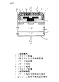
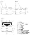
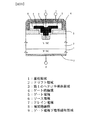
第1の実施形態に係る半導体装置の製造方法により製造された半導体装置について図1を参照して説明する。図1は、本発明の第1の実施形態に係る半導体装置の製造方法により製造された半導体装置の構成を示す断面図である。図1に示す第1の実施形態に係る半導体装置では、電界効果トランジスタの単位セルを2つ対向して並べた構造を備えている。なお、実際には、上記電界効果トランジスタの単位セルが複数並列に配置接続されて1つのトランジスタを形成している。
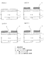
次に、第2の実施形態に係る半導体装置の製造方法について、第1の実施形態に係る半導体装置の製造方法と異なる点を中心に図4を参照して説明する。また、第2の実施形態に係る半導体装置の製造方法により製造された半導体装置は、第1の実施形態に係る半導体装置と全く同じ構造を有している。図4は、本発明の第2の実施形態に係る半導体装置の製造方法を示す断面図である。第2の実施形態に係る半導体装置の製造方法では、第1の実施形態と異なり、第1のマスク材10で覆われていない第1のヘテロ半導体領域3の一部分をエッチングする工程を第1の不純物導入領域11を形成する工程より先に実施する場合を示している。具体的には、図2(2)に示した工程の後、図4(1)に示すように、第1のマスク材10で覆われていない部分において、第1のヘテロ半導体領域3を、例えば反応性イオンエッチング(ドライエッチング)によりエッチングする。次に、図4(2)では、第1のマスク材10で覆われていない部分において、ドリフト領域2中に、例えばイオン注入法を用いて、例えばボロンもしくはアルミなどを不純物導入し、第1の不純物導入領域11を形成する。最後に、第1の実施形態と同様に、図3(5)〜図3(7)の工程を実施し、図1に示した半導体装置と同じ構造の半導体装置を完成させる。これにより、第1のヘテロ半導体領域3と第1の不純物導入領域11の製造順序を逆にしても容易に製造することができる。また、第1の実施形態と同様の効果も取得できる。
次に、第3の実施形態に係る半導体装置の製造方法について、第1の実施形態に係る半導体装置の製造方法と異なる点を中心に図5を参照して説明する。また、第3の実施形態に係る半導体装置の製造方法により製造された半導体装置は、第1の実施形態に係る半導体装置と全く同じ構造を有している。図5は、本発明の第3の実施形態に係る半導体装置の製造方法を示す断面図である。第3の実施形態に係る半導体装置の製造方法では、第1および第2の実施形態と異なり、第1のマスク材10で覆われていない第1のヘテロ半導体領域3の一部分をエッチングする工程で、第1のヘテロ半導体領域3を所定厚み残す場合を示している。具体的には、図2(3)に示した工程の後、図5(1)に示すように、第1のマスク材10で覆われていない部分において、第1のヘテロ半導体領域3を所定厚み残すように、例えば反応性イオンエッチング(ドライエッチング)によりエッチングする。次に、図5(2)では、例えばフッ化アンモニウムとフッ酸との混合溶液で第1のマスク材10をウエットエッチングして除去した後に、例えばドライO2酸化によって、第1のヘテロ半導体領域3の表面を酸化する。特に、図5(1)の工程で残したエッチング残し部分(底部)とエッチングサイド部が所定厚み酸化されるようにする。同時に、第1の不純物導入領域11を活性化し、ゲート電極下電界緩和領域9も形成する。次に、フッ化アンモニウムとフッ酸との混合溶液で、第1のヘテロ半導体領域3の酸化された部分をウエットエッチングして等方的に除去する。最後に、第1の実施形態と同様に、図3(7)の工程を実施し、図1に示した半導体装置と同じ構造の半導体装置を完成させる。これにより、第1のヘテロ半導体領域3の端部とゲート電極下電界緩和領域9が所定距離離れるように形成することができる。また、第1の実施形態と同様の効果も取得できる。更に、エッチング選択比の高いドライエッチとダメージ除去が可能な熱酸化とを組み合わせて、第1のヘテロ半導体領域3を所定厚み残してドライエッチングした後、上記の厚みを酸化することで、ドライエッチング時に生じるプラズマダメージがヘテロ接合駆動端部やドリフト領域2表面に生じなくなり、微細加工が可能となる。これにより、導通動作時において、ダメージによるゲート電界の終端が起こらず、高い導通特性を得ることができる。
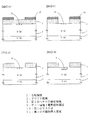
次に、第4の実施形態に係る半導体装置の製造方法について、第1の実施形態に係る半導体装置の製造方法と異なる点を中心に図6を参照して説明する。また、第4の実施形態に係る半導体装置の製造方法により製造された半導体装置は、第1の実施形態に係る半導体装置と全く同じ構造を有している。図6は、本発明の第4の実施形態に係る半導体装置の製造方法を示す断面図である。第4の実施形態では、第1乃至第3の実施形態と異なり、第1のマスク材10の開口部を広げた後、ヘテロ接合駆動端部を形成する場合を示している。具体的には、図2(3)に示した工程の後、図6(1)に示すように、例えばフッ化アンモニウムとフッ酸との混合溶液で第1のマスク材10を所定厚みだけ等方的にウエットエッチングして開口部を広げる。次に、図6(2)では、第1のマスク材10で覆われていない第1のヘテロ半導体領域3の一部分を、例えば反応性イオンエッチング(ドライエッチング)によりエッチングする。次に、図6(3)では、例えばフッ化アンモニウムとフッ酸との混合溶液で第1のマスク材10をウエットエッチングして除去する。次に、図6(4)では、所定の熱処理によって、第1の不純物導入領域11を活性化し、ゲート電極下電界緩和領域9を形成する。最後に、第1の実施形態と同様に、図3(7)の工程を実施し、図1に示した半導体装置と同じ構造の半導体装置を完成させる。これにより、第1乃至第3の実施形態で示した第1のヘテロ半導体領域3の犠牲酸化を用いずとも、容易にヘテロ接合駆動端部とゲート電極下電界緩和領域9が所定距離離れるように形成することができる。また、第1の実施形態と同様の効果も取得できる。
次に、第5の実施形態に係る半導体装置の製造方法について、第1の実施形態と異なる点を中心に図7乃至図9を参照して説明する。また、第5の実施形態に係る半導体装置の製造方法により製造された半導体装置について、第1の実施形態に係る半導体装置と同様の構造には同じ番号を付し、説明を省略する。
次に、第6の実施形態に係る半導体装置の製造方法について、第5の実施形態に係る半導体装置の製造方法と異なる点を中心に図10乃至図11を参照して説明する。また、第6の実施形態に係る半導体装置の製造方法により製造された半導体装置について、第5の実施形態に係る半導体装置と同様の構造には同じ番号を付し、説明を省略する。
次に、第7の実施形態に係る半導体装置の製造方法について、第5の実施形態と異なる点を中心に図12乃至図14を参照して説明する。また、第7の実施形態に係る半導体装置の製造方法により製造された半導体装置について、第5の実施形態に係る半導体装置と同様の構造には同じ番号を付し、説明を省略する。
次に、第8の実施形態に係る半導体装置の製造方法について、第5の実施形態と異なる点を中心に図15乃至図16を参照して説明する。また、第8の実施形態に係る半導体装置の製造方法により製造された半導体装置について、第5の実施形態に係る半導体装置と同様の構造には同じ番号を付し、説明を省略する。
4 ゲート絶縁膜、5 ゲート電極、6 ソース電極、7 ドレイン電極、
8 層間絶縁膜、9 ゲート電極下電界緩和領域、10 第1のマスク材、
11 第1の不純物導入領域、12 ソース領域下電界緩和領域、
13 第2の不純物導入領域、14 第2のマスク材、
15 第3の不純物導入領域、16 第3のマスク材、
17 第2のヘテロ半導体領域、18 導通領域
Claims (15)
- 半導体基体と、
前記半導体基体と異なるバンドギャップを有する半導体材料から成り、前記半導体基体とヘテロ接合し、且つ前記半導体基体の表面の一部に設けられたヘテロ半導体領域と、
少なくとも前記ヘテロ半導体領域の側面及び前記ヘテロ半導体領域が形成されていない前記半導体基体の表面にまたがって形成されたゲート絶縁膜と、
前記ゲート絶縁膜に接して形成されたゲート電極と、
前記半導体基体及び前記ヘテロ半導体領域が前記ゲート絶縁膜に同時に接するヘテロ接合駆動端部から所定距離離れて、前記半導体基体および前記ゲート絶縁膜に接する第1の電界緩和領域と、
前記ヘテロ半導体領域とオーミック接続されたソース電極と、
前記半導体基体とオーミック接続されたドレイン電極とを有する半導体装置の製造方法において、
前記半導体基体上に前記ヘテロ半導体領域を形成する工程と、
所定形状にパターニングされた第1のマスク材を前記へテロ半導体領域上に形成する工程と、
前記第1のマスク材で覆われていない部分の前記半導体基体に前記第1の電界緩和領域を形成する工程と、
前記第1の電界緩和領域を形成後に前記第1のマスク材で覆われていない部分よりも広く前記ヘテロ半導体領域を選択的に除去する工程と、
前記ゲート絶縁膜を形成する工程と
を含むことを特徴とする半導体装置の製造方法。 - 前記第1の電界緩和領域を形成する際、前記第1のマスク材で覆われていない前記半導体基体に、イオン注入法を用いて所定の不純物を導入することを特徴とする請求項1記載の半導体装置の製造方法。
- 前記第1の電界緩和領域を形成する際、前記不純物を活性化する処理を行うことを特徴とする請求項2に記載の半導体装置の製造方法。
- 半導体基体と、
前記半導体基体と異なるバンドギャップを有する半導体材料から成り、前記半導体基体とヘテロ接合し、且つ前記半導体基体の表面の一部に設けられたヘテロ半導体領域と、
少なくとも前記ヘテロ半導体領域の側面及び前記ヘテロ半導体領域が形成されていない前記半導体基体の表面にまたがって形成されたゲート絶縁膜と、
前記ゲート絶縁膜に接して形成されたゲート電極と、
前記半導体基体及び前記ヘテロ半導体領域が前記ゲート絶縁膜に同時に接するヘテロ接合駆動端部から所定距離離れて、前記半導体基体および前記ゲート絶縁膜に接する第1の電界緩和領域と、
前記ヘテロ半導体領域とオーミック接続されたソース電極と、
前記半導体基体とオーミック接続されたドレイン電極と、
前記半導体基体および前記ヘテロ半導体領域に接し、前記ヘテロ接合駆動端部から所定距離離れて形成された第2の電界緩和領域とを有する半導体装置の製造方法において、
前記半導体基体上に前記ヘテロ半導体領域を形成する工程と、
所定形状にパターニングされた第1のマスク材を前記へテロ半導体領域上に形成する工程と、
前記第1のマスク材で覆われていない部分の前記半導体基体に前記第1の電界緩和領域及び前記第2の電界緩和領域を形成する工程と、
所定形状にパターニングされた第2のマスク材を前記第1のマスク材及び前記ヘテロ半導体領域の上に形成する工程と、
前記第1のマスク材及び前記第2のマスク材で覆われていない部分よりも広く前記ヘテロ半導体領域を選択的に除去する工程と、
前記ゲート絶縁膜を形成する工程と
を含むことを特徴とする半導体装置の製造方法。 - 前記第2の電界緩和領域と接する前記ヘテロ半導体領域を覆い隠す第2のマスク材を前記へテロ半導体領域上に形成する工程と含み、
前記第1のマスク材と前記第2のマスク材を共用して、前記ヘテロ接合駆動端部を形成することを特徴とする請求項4に記載の半導体装置の製造方法。 - 前記第2のマスク材の材質が、前記第1のマスク材の材質と異なることを特徴とする請求項5に記載の半導体装置の製造方法。
- 前記第2の電界緩和領域と接しない前記へテロ半導体領域を、前記第1のマスク材とともに覆い隠す第3のマスク材を前記へテロ半導体領域上に形成する工程と、
前記第2の電界緩和領域と接する前記ヘテロ半導体領域を覆い隠す第2のマスク材を前記へテロ半導体領域上に形成する工程と含み、
前記第1のマスク材および前記第3のマスク材を共用して、前記第2の電界緩和領域を形成し、
前記第1のマスク材および前記第2のマスク材を共用して、前記ヘテロ接合駆動端部を形成することを特徴とする請求項4に記載の半導体装置の製造方法。 - 前記第2のマスク材もしくは前記第3のマスク材のいずれか一方もしくは両方の材質が、前記第1のマスク材の材質と異なることを特徴とする請求項7に記載の半導体装置の製造方法。
- 前記第2の電界緩和領域を形成する際、前記第1のマスク材で覆われていない前記半導体基体に、イオン注入法を用いて所定の不純物を導入することを特徴とする請求項4乃至8のいずれかに記載の半導体装置の製造方法。
- 前記第2の電界緩和領域を形成する際、前記不純物を活性化するべく熱処理を行うことを特徴とする請求項9に記載の半導体装置の製造方法。
- 前記ヘテロ接合駆動端部を形成する際、前記第1のマスク材で覆われていない前記へテロ半導体領域の少なくとも一部を等方的に除去する工程を有することを特徴とする請求項4乃至10のいずれかに記載の半導体装置の製造方法。
- 前記等方的に除去する工程を犠牲酸化によっておこなうことを特徴とする請求項11に記載の半導体装置の製造方法。
- 前記ヘテロ接合駆動端部を形成する際、前記第1のマスク材の少なくとも一部を等方的に除去した後、前記ヘテロ接合駆動端部を形成することを特徴とする前記請求項1乃至3のいずれかに記載の半導体装置の製造方法。
- 前記半導体基体が炭化珪素、ダイヤモンドまたは窒化ガリウムからなることを特徴とする前記請求項1乃至13のいずれかに記載の半導体装置の製造方法。
- 前記ヘテロ半導体領域が単結晶シリコン、多結晶シリコンまたはアモルファスシリコンからなることを特徴とする請求項1乃至14のいずれかに記載の半導体装置の製造方法。
Priority Applications (5)
| Application Number | Priority Date | Filing Date | Title |
|---|---|---|---|
| JP2006316807A JP5211468B2 (ja) | 2006-11-24 | 2006-11-24 | 半導体装置の製造方法 |
| US11/870,561 US7605017B2 (en) | 2006-11-24 | 2007-10-11 | Method of manufacturing a semiconductor device and products made thereby |
| CN2007101937011A CN101188201B (zh) | 2006-11-24 | 2007-11-22 | 制造半导体器件的方法 |
| KR1020070120083A KR100944056B1 (ko) | 2006-11-24 | 2007-11-23 | 반도체 장치 제조 방법 및 그에 의해 제조되는 제품 |
| EP07121480.3A EP1926147B1 (en) | 2006-11-24 | 2007-11-26 | Method of manufacturing a semiconductor device and products made thereby |
Applications Claiming Priority (1)
| Application Number | Priority Date | Filing Date | Title |
|---|---|---|---|
| JP2006316807A JP5211468B2 (ja) | 2006-11-24 | 2006-11-24 | 半導体装置の製造方法 |
Publications (2)
| Publication Number | Publication Date |
|---|---|
| JP2008130959A JP2008130959A (ja) | 2008-06-05 |
| JP5211468B2 true JP5211468B2 (ja) | 2013-06-12 |
Family
ID=39092901
Family Applications (1)
| Application Number | Title | Priority Date | Filing Date |
|---|---|---|---|
| JP2006316807A Active JP5211468B2 (ja) | 2006-11-24 | 2006-11-24 | 半導体装置の製造方法 |
Country Status (5)
| Country | Link |
|---|---|
| US (1) | US7605017B2 (ja) |
| EP (1) | EP1926147B1 (ja) |
| JP (1) | JP5211468B2 (ja) |
| KR (1) | KR100944056B1 (ja) |
| CN (1) | CN101188201B (ja) |
Families Citing this family (22)
| Publication number | Priority date | Publication date | Assignee | Title |
|---|---|---|---|---|
| US8067776B2 (en) * | 2007-06-08 | 2011-11-29 | Nissan Motor Co., Ltd. | Method of manufacturing semiconductor device and semiconductor device manufactured thereof |
| US8735906B2 (en) * | 2009-04-13 | 2014-05-27 | Rohm Co., Ltd. | Semiconductor device and method of manufacturing semiconductor device |
| JP2012099601A (ja) * | 2010-11-01 | 2012-05-24 | Sumitomo Electric Ind Ltd | 半導体装置およびその製造方法 |
| US8742460B2 (en) | 2010-12-15 | 2014-06-03 | Transphorm Inc. | Transistors with isolation regions |
| US8643062B2 (en) | 2011-02-02 | 2014-02-04 | Transphorm Inc. | III-N device structures and methods |
| US8598937B2 (en) | 2011-10-07 | 2013-12-03 | Transphorm Inc. | High power semiconductor electronic components with increased reliability |
| US9093366B2 (en) | 2012-04-09 | 2015-07-28 | Transphorm Inc. | N-polar III-nitride transistors |
| US9184275B2 (en) | 2012-06-27 | 2015-11-10 | Transphorm Inc. | Semiconductor devices with integrated hole collectors |
| US9087718B2 (en) | 2013-03-13 | 2015-07-21 | Transphorm Inc. | Enhancement-mode III-nitride devices |
| US9245992B2 (en) | 2013-03-15 | 2016-01-26 | Transphorm Inc. | Carbon doping semiconductor devices |
| JP5939448B2 (ja) * | 2013-04-30 | 2016-06-22 | 日産自動車株式会社 | 半導体装置及びその製造方法 |
| WO2015009514A1 (en) | 2013-07-19 | 2015-01-22 | Transphorm Inc. | Iii-nitride transistor including a p-type depleting layer |
| US9318593B2 (en) | 2014-07-21 | 2016-04-19 | Transphorm Inc. | Forming enhancement mode III-nitride devices |
| US9536966B2 (en) | 2014-12-16 | 2017-01-03 | Transphorm Inc. | Gate structures for III-N devices |
| US9536967B2 (en) | 2014-12-16 | 2017-01-03 | Transphorm Inc. | Recessed ohmic contacts in a III-N device |
| CN105023939A (zh) * | 2015-04-08 | 2015-11-04 | 四川大学 | 一种新型的栅下阱结构4H-SiCMOSFET器件 |
| ITUB20155536A1 (it) | 2015-11-12 | 2017-05-12 | St Microelectronics Srl | Transistore hemt di tipo normalmente spento includente una trincea contenente una regione di gate e formante almeno un gradino, e relativo procedimento di fabbricazione |
| CN108604597B (zh) | 2016-01-15 | 2021-09-17 | 创世舫电子有限公司 | 具有al(1-x)sixo栅极绝缘体的增强模式iii-氮化物器件 |
| TWI762486B (zh) | 2016-05-31 | 2022-05-01 | 美商創世舫科技有限公司 | 包含漸變空乏層的三族氮化物裝置 |
| JP6237845B1 (ja) * | 2016-08-24 | 2017-11-29 | 富士電機株式会社 | 縦型mosfetおよび縦型mosfetの製造方法 |
| CN111668101B (zh) * | 2020-06-03 | 2022-07-01 | 西安电子科技大学 | 一种增强型氮化镓高电子迁移率晶体管及其制备方法 |
| CN114709255A (zh) * | 2022-04-02 | 2022-07-05 | 东南大学 | 基于异质结的高功率密度隧穿半导体器件及其制造工艺 |
Family Cites Families (12)
| Publication number | Priority date | Publication date | Assignee | Title |
|---|---|---|---|---|
| JP3620513B2 (ja) | 2002-04-26 | 2005-02-16 | 日産自動車株式会社 | 炭化珪素半導体装置 |
| US7282739B2 (en) * | 2002-04-26 | 2007-10-16 | Nissan Motor Co., Ltd. | Silicon carbide semiconductor device |
| EP2560210B1 (en) | 2003-09-24 | 2018-11-28 | Nissan Motor Co., Ltd. | Semiconductor device and manufacturing method thereof |
| JP4033150B2 (ja) * | 2004-03-09 | 2008-01-16 | 日産自動車株式会社 | 半導体装置とその製造方法 |
| EP1638149B1 (fr) * | 2004-09-15 | 2011-11-23 | STMicroelectronics (Crolles 2) SAS | Procédé de fabrication d'un transistor à effet de champ à grille isolée à canal à hétérostructure |
| US20060060917A1 (en) * | 2004-09-17 | 2006-03-23 | Nissan Motor Co., Ltd. | Semiconductor device and method of manufacturing semiconductor device |
| EP1641030B1 (en) | 2004-09-28 | 2012-01-11 | Nissan Motor Co., Ltd. | Method of manufacturing a semiconductor device |
| JP2006100365A (ja) * | 2004-09-28 | 2006-04-13 | Nissan Motor Co Ltd | 半導体装置 |
| JP5044885B2 (ja) * | 2004-09-28 | 2012-10-10 | 日産自動車株式会社 | 半導体装置及びその製造方法 |
| US7588961B2 (en) * | 2005-03-30 | 2009-09-15 | Nissan Motor Co., Ltd. | Semiconductor device and manufacturing method thereof |
| US8441036B2 (en) * | 2006-03-22 | 2013-05-14 | Nissan Motor Co., Ltd. | Semiconductor device and method of manufacturing the same |
| JP5098214B2 (ja) * | 2006-04-28 | 2012-12-12 | 日産自動車株式会社 | 半導体装置およびその製造方法 |
-
2006
- 2006-11-24 JP JP2006316807A patent/JP5211468B2/ja active Active
-
2007
- 2007-10-11 US US11/870,561 patent/US7605017B2/en active Active
- 2007-11-22 CN CN2007101937011A patent/CN101188201B/zh active Active
- 2007-11-23 KR KR1020070120083A patent/KR100944056B1/ko active IP Right Grant
- 2007-11-26 EP EP07121480.3A patent/EP1926147B1/en active Active
Also Published As
| Publication number | Publication date |
|---|---|
| EP1926147B1 (en) | 2018-01-17 |
| EP1926147A2 (en) | 2008-05-28 |
| EP1926147A3 (en) | 2009-03-04 |
| CN101188201B (zh) | 2010-11-10 |
| KR100944056B1 (ko) | 2010-02-24 |
| US20080121933A1 (en) | 2008-05-29 |
| KR20080047294A (ko) | 2008-05-28 |
| CN101188201A (zh) | 2008-05-28 |
| JP2008130959A (ja) | 2008-06-05 |
| US7605017B2 (en) | 2009-10-20 |
Similar Documents
| Publication | Publication Date | Title |
|---|---|---|
| JP5211468B2 (ja) | 半導体装置の製造方法 | |
| JP5228291B2 (ja) | 半導体装置の製造方法 | |
| JP5034278B2 (ja) | 半導体装置の製造方法 | |
| JP5194380B2 (ja) | 半導体装置 | |
| EP1837915B1 (en) | Semiconductors | |
| JP4033150B2 (ja) | 半導体装置とその製造方法 | |
| JP3975992B2 (ja) | 半導体装置及びその製造方法 | |
| JP4862254B2 (ja) | 半導体装置の製造方法 | |
| US7531396B2 (en) | Method of manufacturing semiconductor device | |
| JP4736386B2 (ja) | 半導体装置の製造方法 | |
| JP5044885B2 (ja) | 半導体装置及びその製造方法 | |
| JP2006100329A (ja) | 半導体装置の製造方法および半導体装置 | |
| JP5194575B2 (ja) | 半導体装置の製造方法 | |
| JP2006100365A (ja) | 半導体装置 | |
| EP1835543B1 (en) | Method for manufacturing a semiconductor device | |
| JP2006086397A (ja) | 半導体装置およびその製造方法 | |
| KR100691598B1 (ko) | 반도체 장치의 제조 방법 | |
| JP5211472B2 (ja) | 半導体装置及びその製造方法 | |
| JP5729356B2 (ja) | 半導体装置 | |
| JP5211479B2 (ja) | 半導体装置および半導体装置の製造方法 |
Legal Events
| Date | Code | Title | Description |
|---|---|---|---|
| A621 | Written request for application examination |
Free format text: JAPANESE INTERMEDIATE CODE: A621 Effective date: 20091027 |
|
| A521 | Written amendment |
Free format text: JAPANESE INTERMEDIATE CODE: A523 Effective date: 20100209 |
|
| RD02 | Notification of acceptance of power of attorney |
Free format text: JAPANESE INTERMEDIATE CODE: A7422 Effective date: 20101018 |
|
| RD04 | Notification of resignation of power of attorney |
Free format text: JAPANESE INTERMEDIATE CODE: A7424 Effective date: 20101028 |
|
| A977 | Report on retrieval |
Free format text: JAPANESE INTERMEDIATE CODE: A971007 Effective date: 20120816 |
|
| A131 | Notification of reasons for refusal |
Free format text: JAPANESE INTERMEDIATE CODE: A131 Effective date: 20120821 |
|
| A521 | Written amendment |
Free format text: JAPANESE INTERMEDIATE CODE: A523 Effective date: 20121022 |
|
| A131 | Notification of reasons for refusal |
Free format text: JAPANESE INTERMEDIATE CODE: A131 Effective date: 20121113 |
|
| A521 | Written amendment |
Free format text: JAPANESE INTERMEDIATE CODE: A523 Effective date: 20130109 |
|
| TRDD | Decision of grant or rejection written | ||
| A01 | Written decision to grant a patent or to grant a registration (utility model) |
Free format text: JAPANESE INTERMEDIATE CODE: A01 Effective date: 20130129 |
|
| A61 | First payment of annual fees (during grant procedure) |
Free format text: JAPANESE INTERMEDIATE CODE: A61 Effective date: 20130211 |
|
| R150 | Certificate of patent or registration of utility model |
Ref document number: 5211468 Country of ref document: JP Free format text: JAPANESE INTERMEDIATE CODE: R150 Free format text: JAPANESE INTERMEDIATE CODE: R150 |
|
| FPAY | Renewal fee payment (event date is renewal date of database) |
Free format text: PAYMENT UNTIL: 20160308 Year of fee payment: 3 |