JP5192068B2 - 発光装置、および発光装置を備えた光照射装置 - Google Patents
発光装置、および発光装置を備えた光照射装置 Download PDFInfo
- Publication number
- JP5192068B2 JP5192068B2 JP2011203663A JP2011203663A JP5192068B2 JP 5192068 B2 JP5192068 B2 JP 5192068B2 JP 2011203663 A JP2011203663 A JP 2011203663A JP 2011203663 A JP2011203663 A JP 2011203663A JP 5192068 B2 JP5192068 B2 JP 5192068B2
- Authority
- JP
- Japan
- Prior art keywords
- light
- light emitting
- wavelength
- emitting device
- peak
- Prior art date
- Legal status (The legal status is an assumption and is not a legal conclusion. Google has not performed a legal analysis and makes no representation as to the accuracy of the status listed.)
- Expired - Fee Related
Links
Images


Classifications
-
- F—MECHANICAL ENGINEERING; LIGHTING; HEATING; WEAPONS; BLASTING
- F21—LIGHTING
- F21K—NON-ELECTRIC LIGHT SOURCES USING LUMINESCENCE; LIGHT SOURCES USING ELECTROCHEMILUMINESCENCE; LIGHT SOURCES USING CHARGES OF COMBUSTIBLE MATERIAL; LIGHT SOURCES USING SEMICONDUCTOR DEVICES AS LIGHT-GENERATING ELEMENTS; LIGHT SOURCES NOT OTHERWISE PROVIDED FOR
- F21K2/00—Non-electric light sources using luminescence; Light sources using electrochemiluminescence
-
- A—HUMAN NECESSITIES
- A01—AGRICULTURE; FORESTRY; ANIMAL HUSBANDRY; HUNTING; TRAPPING; FISHING
- A01G—HORTICULTURE; CULTIVATION OF VEGETABLES, FLOWERS, RICE, FRUIT, VINES, HOPS OR SEAWEED; FORESTRY; WATERING
- A01G7/00—Botany in general
- A01G7/04—Electric or magnetic or acoustic treatment of plants for promoting growth
- A01G7/045—Electric or magnetic or acoustic treatment of plants for promoting growth with electric lighting
-
- A—HUMAN NECESSITIES
- A01—AGRICULTURE; FORESTRY; ANIMAL HUSBANDRY; HUNTING; TRAPPING; FISHING
- A01G—HORTICULTURE; CULTIVATION OF VEGETABLES, FLOWERS, RICE, FRUIT, VINES, HOPS OR SEAWEED; FORESTRY; WATERING
- A01G9/00—Cultivation in receptacles, forcing-frames or greenhouses; Edging for beds, lawn or the like
- A01G9/24—Devices or systems for heating, ventilating, regulating temperature, illuminating, or watering, in greenhouses, forcing-frames, or the like
- A01G9/249—Lighting means
-
- H—ELECTRICITY
- H01—ELECTRIC ELEMENTS
- H01L—SEMICONDUCTOR DEVICES NOT COVERED BY CLASS H10
- H01L33/00—Semiconductor devices with at least one potential-jump barrier or surface barrier specially adapted for light emission; Processes or apparatus specially adapted for the manufacture or treatment thereof or of parts thereof; Details thereof
- H01L33/48—Semiconductor devices with at least one potential-jump barrier or surface barrier specially adapted for light emission; Processes or apparatus specially adapted for the manufacture or treatment thereof or of parts thereof; Details thereof characterised by the semiconductor body packages
- H01L33/50—Wavelength conversion elements
-
- F—MECHANICAL ENGINEERING; LIGHTING; HEATING; WEAPONS; BLASTING
- F21—LIGHTING
- F21Y—INDEXING SCHEME ASSOCIATED WITH SUBCLASSES F21K, F21L, F21S and F21V, RELATING TO THE FORM OR THE KIND OF THE LIGHT SOURCES OR OF THE COLOUR OF THE LIGHT EMITTED
- F21Y2101/00—Point-like light sources
-
- F—MECHANICAL ENGINEERING; LIGHTING; HEATING; WEAPONS; BLASTING
- F21—LIGHTING
- F21Y—INDEXING SCHEME ASSOCIATED WITH SUBCLASSES F21K, F21L, F21S and F21V, RELATING TO THE FORM OR THE KIND OF THE LIGHT SOURCES OR OF THE COLOUR OF THE LIGHT EMITTED
- F21Y2105/00—Planar light sources
- F21Y2105/10—Planar light sources comprising a two-dimensional array of point-like light-generating elements
- F21Y2105/12—Planar light sources comprising a two-dimensional array of point-like light-generating elements characterised by the geometrical disposition of the light-generating elements, e.g. arranging light-generating elements in differing patterns or densities
-
- F—MECHANICAL ENGINEERING; LIGHTING; HEATING; WEAPONS; BLASTING
- F21—LIGHTING
- F21Y—INDEXING SCHEME ASSOCIATED WITH SUBCLASSES F21K, F21L, F21S and F21V, RELATING TO THE FORM OR THE KIND OF THE LIGHT SOURCES OR OF THE COLOUR OF THE LIGHT EMITTED
- F21Y2115/00—Light-generating elements of semiconductor light sources
- F21Y2115/10—Light-emitting diodes [LED]
-
- H—ELECTRICITY
- H01—ELECTRIC ELEMENTS
- H01L—SEMICONDUCTOR DEVICES NOT COVERED BY CLASS H10
- H01L2224/00—Indexing scheme for arrangements for connecting or disconnecting semiconductor or solid-state bodies and methods related thereto as covered by H01L24/00
- H01L2224/01—Means for bonding being attached to, or being formed on, the surface to be connected, e.g. chip-to-package, die-attach, "first-level" interconnects; Manufacturing methods related thereto
- H01L2224/42—Wire connectors; Manufacturing methods related thereto
- H01L2224/47—Structure, shape, material or disposition of the wire connectors after the connecting process
- H01L2224/48—Structure, shape, material or disposition of the wire connectors after the connecting process of an individual wire connector
- H01L2224/481—Disposition
- H01L2224/48151—Connecting between a semiconductor or solid-state body and an item not being a semiconductor or solid-state body, e.g. chip-to-substrate, chip-to-passive
- H01L2224/48221—Connecting between a semiconductor or solid-state body and an item not being a semiconductor or solid-state body, e.g. chip-to-substrate, chip-to-passive the body and the item being stacked
- H01L2224/48245—Connecting between a semiconductor or solid-state body and an item not being a semiconductor or solid-state body, e.g. chip-to-substrate, chip-to-passive the body and the item being stacked the item being metallic
- H01L2224/48247—Connecting between a semiconductor or solid-state body and an item not being a semiconductor or solid-state body, e.g. chip-to-substrate, chip-to-passive the body and the item being stacked the item being metallic connecting the wire to a bond pad of the item
-
- H—ELECTRICITY
- H01—ELECTRIC ELEMENTS
- H01L—SEMICONDUCTOR DEVICES NOT COVERED BY CLASS H10
- H01L25/00—Assemblies consisting of a plurality of individual semiconductor or other solid state devices ; Multistep manufacturing processes thereof
- H01L25/03—Assemblies consisting of a plurality of individual semiconductor or other solid state devices ; Multistep manufacturing processes thereof all the devices being of a type provided for in the same subgroup of groups H01L27/00 - H01L33/00, or in a single subclass of H10K, H10N, e.g. assemblies of rectifier diodes
- H01L25/04—Assemblies consisting of a plurality of individual semiconductor or other solid state devices ; Multistep manufacturing processes thereof all the devices being of a type provided for in the same subgroup of groups H01L27/00 - H01L33/00, or in a single subclass of H10K, H10N, e.g. assemblies of rectifier diodes the devices not having separate containers
- H01L25/075—Assemblies consisting of a plurality of individual semiconductor or other solid state devices ; Multistep manufacturing processes thereof all the devices being of a type provided for in the same subgroup of groups H01L27/00 - H01L33/00, or in a single subclass of H10K, H10N, e.g. assemblies of rectifier diodes the devices not having separate containers the devices being of a type provided for in group H01L33/00
- H01L25/0753—Assemblies consisting of a plurality of individual semiconductor or other solid state devices ; Multistep manufacturing processes thereof all the devices being of a type provided for in the same subgroup of groups H01L27/00 - H01L33/00, or in a single subclass of H10K, H10N, e.g. assemblies of rectifier diodes the devices not having separate containers the devices being of a type provided for in group H01L33/00 the devices being arranged next to each other
-
- Y—GENERAL TAGGING OF NEW TECHNOLOGICAL DEVELOPMENTS; GENERAL TAGGING OF CROSS-SECTIONAL TECHNOLOGIES SPANNING OVER SEVERAL SECTIONS OF THE IPC; TECHNICAL SUBJECTS COVERED BY FORMER USPC CROSS-REFERENCE ART COLLECTIONS [XRACs] AND DIGESTS
- Y02—TECHNOLOGIES OR APPLICATIONS FOR MITIGATION OR ADAPTATION AGAINST CLIMATE CHANGE
- Y02P—CLIMATE CHANGE MITIGATION TECHNOLOGIES IN THE PRODUCTION OR PROCESSING OF GOODS
- Y02P60/00—Technologies relating to agriculture, livestock or agroalimentary industries
- Y02P60/14—Measures for saving energy, e.g. in green houses
Description
(1)1種類のLEDチップのみを使用するため、従来の2種類のLEDチップを使用したときに比べて、表面実装型発光部の面積が小さくて済む。
(2)蛍光体は蛍光体含有封止樹脂に分散され、かつ、第1のLEDチップを覆っていることから、従来に比べて、第1光および第3光の混色が良好である。この結果、従来の各種のLEDチップの個々の距離が離れているために、被照射体において色ムラ(第1光および第3光を合成した光の強度ムラ)が生じることを効果的に抑えることができる。例えば、光合成光量子束の比が求めた比にならないという問題を容易に解決できる。
(3)蛍光体を樹脂に所定の配合比にて分散させることが可能であり、その配合比に応じて短波長域と長波長域における光量を変化させることができる。
本発明の一実施形態について図1〜3に基づいて説明すれば、以下のとおりである。
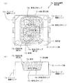
本実施の形態の発光装置1の構成について、図1に基づいて説明する。図1は、本実施の形態に係る発光装置1の構成を示す説明図である。図1の(a)は本実施の形態に係る発光装置1の要部構成を示す正面図である。また、図1の(b)は図1の(a)の矢符B方向から見た側面図である。また、図1の(c)は図1の(a)の矢符C方向から見た側面図である。
次に、発光装置1が備える本実施の形態の表面実装型発光部10aについて、図2に基づいて説明する。
(1)1種類のLEDチップのみを使用するため、従来の2種類のLEDチップを使用したときに比べて、表面実装型発光部の面積が小さくて済む。
(2)蛍光体は蛍光体含有封止樹脂に分散され、かつ、第1のLEDチップを覆っていることから、従来に比べて、第1光および第3光の混色が良好である。この結果、従来の各種のLEDチップの個々の距離が離れているために、被照射体において色ムラ(第1光および第3光を合成した光の強度ムラ)が生じることを効果的に抑えることができる。例えば、光合成光量子束の比が求めた比にならないという問題を容易に解決できる。
(3)蛍光体を樹脂に所定の配合比にて分散させることが可能であり、その配合比に応じて短波長域と長波長域における光量を変化させることができる。
本実施の形態の表面実装型発光部10aにおける青色域と赤色域との光量割合の調整について、図3および図4に基づいて説明する。
次に、植物の成長においてどのような波長の光を照射すればよいのかについて、図5に基づいて説明する。図5は、クロロフィルの光吸収特性と本実施の形態の表面実装型発光部10aの発光スペクトルを示す図である。
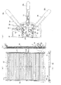
次に、図6に基づいて、表面実装型発光部10aを配線基板20に実装する一例について説明する。
表面実装型発光部10aは、図2に示すように、表面実装用の外部端子であるカソード電極ランド11aおよびアノード電極ランド11bを有するので、配線基板20の表面にそのまま載置され実装(接続)される。したがって、接続構造を簡単にすることができ、接続(実装)の作業性、信頼性を向上させることができる。
配線基板20の平面形状は、例えば160mm×160mmの矩形である。また、配線基板20の厚さは、例えば1mmである。また、16行×16列のドットマトリックス状に配置された表面実装型発光部10aは、列方向の配置ピッチが10mm、行方向の配置ピッチが10mmである。
また、本実施の形態に係るレンズ部30は、凸レンズとしての集光特性を有する曲面部(曲面を有する部材)30aと、曲面部30aから枠体部40まで延長され曲面部30aを保持する保持部30bとを備えている。図6に示す例では、保持部30bが、曲面部30aの周囲に突出して形成され、枠体部40の1マス毎に、矩形の輪状に形成された溝部に嵌め込まれるようになっている。
各表面実装型発光部10a(より具体的には、各表面実装型発光部10aと、レンズ部30と、枠体部40と)に対応させて立壁部60が配置される。立壁部60は、枠体部40の行方向に対応させて配置されている。つまり、立壁部60は、図1で示したとおり、発光装置1が備える表面実装型発光部10aの16行に対応させて16個配置されている。
なお、本実施の形態に記載された発光装置1が備える表面実装型発光部は、前記表面実装型発光部10aに限定することなく、例えば、図7に記載された表面実装型発光部10bに置き換えてもよい。
前記実施の形態1にて説明した表面実装型発光部10aは、クロロフィルの青色域吸収ピークに対応すべく短波長域400nm〜480nmの範囲でピーク波長を有する少なくとも1個の青色LEDチップ14aを有していた。
本発明の他の実施の形態について、図8および図9に基づいて説明すれば、以下のとおりである。なお、本実施の形態において説明すること以外の構成は、前記実施の形態1と同じである。また、説明の便宜上、前記の実施の形態1の図面に示した部材と同一の機能を有する部材については、同一の符号を付し、その説明を省略する。
図8は、本発明の実施の形態2に係る発光装置1’の概要を示す正面図である。
発光装置1’が備える表面実装型発光部10aの構成は、実施の形態1に説明したものと同様であるため、その説明を省略する。ここで、図9に基づいて、表面実装型発光部10cの構成についてのみ説明する。
特許文献1および2に記載された光源の構成では、光源の正面における照度が不十分になるという問題が有る。
(A)赤色LEDを高輝度発光させる(駆動電流を増加する)か、
(B)各LEDに搭載する赤LEDチップ数を増やすか、
(C)赤色LEDの個数を増やすか、
等の措置が必要となる。

ここで、色素クロロフィルについて記載したがそれに限定することなく、光合成色素であればよく、例えば、カロテノイド、フィコピリンなどが挙げられる。さらに生物、植物としてラン藻類、紅藻類、ケイ藻類、褐藻類、緑藻類、種子植物(コケ、シダ)、光合成細菌などの光従属栄養的生物全般が挙げられる。
10a、10b、10c 表面実装型発光部
14a 青色LEDチップ(第1のLEDチップ)
14b 青色LEDチップ(第2のLEDチップ)
17 樹脂層(蛍光体含有封止樹脂)
17b 赤蛍光体(蛍光体)
20 配線基板
30 レンズ部
40 枠体部
60 立壁部
Claims (7)
- 配線基板の表面に実装された表面実装型発光部と、
上記表面実装型発光部の光出射側に配されたレンズ部と、
上記レンズ部の周囲を固定する枠体部とを備え、
上記表面実装型発光部は、
生育に光を必要とする生物によって吸収される光の複数のピーク波長のうち、相対的に短波長域の第1のピーク波長に対応した第1光を発する、少なくとも1個の第1のLEDチップと、
上記第1のLEDチップを覆う蛍光体含有封止樹脂とを備え、
上記蛍光体含有封止樹脂に含有された蛍光体は、上記第1のLEDチップが出射する第1光を吸収することにより、上記複数のピーク波長のうち、相対的に長波長域のピーク波長に対応した第3光を発し、
上記表面実装型発光部を含む複数の表面実装型発光部が、行列状に配置され、
上記枠体部は、上記複数の表面実装型発光部に対応して、格子状の形状を備え、
格子状の上記枠体部の1マス毎に、上記レンズ部が設けられており、
上記複数の表面実装型発光部のうち、列方向に沿って隣接する表面実装型発光部の各間に、上記枠体部に対して、光出射側に立ち上がる立壁部が、上記列方向と交差する行方向に連続して設けられており、
上記立壁部は、上記配線基板の表面に対して、垂直な状態と傾斜した状態との間で回動可能に構成されていること
を特徴とする発光装置。 - 上記表面実装型発光部は、
上記複数のピーク波長のうち、上記短波長域の第2のピーク波長であって、上記第1のピーク波長とは異なる第2のピーク波長に対応した第2光を発する、少なくとも1個の第2のLEDチップを備えていること
を特徴とする請求項1に記載の発光装置。 - 上記レンズ部と上記枠体部とは、レンズモジュールとして一体的に構成されていることを特徴とする請求項1または2に記載の発光装置。
- 上記第1のピーク波長に対応した第1光の波長は、400nm以上480nm以下の範囲を有し、
上記長波長域のピーク波長に対応した第3光の波長は、620nm以上700nm以下の範囲を有していること
を特徴とする請求項1または2に記載の発光装置。 - 上記第2のピーク波長に対応した第2光の波長は、400nm以上450nm以下の範囲を有していること
を特徴とする請求項2に記載の発光装置。 - 上記表面実装型発光部において、上記第1光および第3光を含む光が出射される開口部は、短辺および長辺を有した長方形の形状を有すること
を特徴とする請求項1〜5のいずれか1項に記載の発光装置。 - 請求項1〜6のいずれか1項に記載の発光装置を、栽培または培養を含む生物育成用の光源として備えていることを特徴とする光照射装置。
Priority Applications (5)
| Application Number | Priority Date | Filing Date | Title |
|---|---|---|---|
| JP2011203663A JP5192068B2 (ja) | 2011-09-16 | 2011-09-16 | 発光装置、および発光装置を備えた光照射装置 |
| EP12832671.7A EP2757601B1 (en) | 2011-09-16 | 2012-08-21 | Light emitting apparatus, and light irradiation apparatus provided with light emitting apparatus |
| CN201280043350.5A CN103765617A (zh) | 2011-09-16 | 2012-08-21 | 发光装置以及具备发光装置的光照射装置 |
| US14/343,084 US9400088B2 (en) | 2011-09-16 | 2012-08-21 | Light emitting apparatus, and light irradiation apparatus provided with light emitting apparatus |
| PCT/JP2012/071106 WO2013038878A1 (ja) | 2011-09-16 | 2012-08-21 | 発光装置、および発光装置を備えた光照射装置 |
Applications Claiming Priority (1)
| Application Number | Priority Date | Filing Date | Title |
|---|---|---|---|
| JP2011203663A JP5192068B2 (ja) | 2011-09-16 | 2011-09-16 | 発光装置、および発光装置を備えた光照射装置 |
Related Child Applications (1)
| Application Number | Title | Priority Date | Filing Date |
|---|---|---|---|
| JP2013016191A Division JP5394583B2 (ja) | 2013-01-30 | 2013-01-30 | 発光装置、および発光装置を備えた光照射装置 |
Publications (2)
| Publication Number | Publication Date |
|---|---|
| JP2013065709A JP2013065709A (ja) | 2013-04-11 |
| JP5192068B2 true JP5192068B2 (ja) | 2013-05-08 |
Family
ID=47883112
Family Applications (1)
| Application Number | Title | Priority Date | Filing Date |
|---|---|---|---|
| JP2011203663A Expired - Fee Related JP5192068B2 (ja) | 2011-09-16 | 2011-09-16 | 発光装置、および発光装置を備えた光照射装置 |
Country Status (5)
| Country | Link |
|---|---|
| US (1) | US9400088B2 (ja) |
| EP (1) | EP2757601B1 (ja) |
| JP (1) | JP5192068B2 (ja) |
| CN (1) | CN103765617A (ja) |
| WO (1) | WO2013038878A1 (ja) |
Families Citing this family (6)
| Publication number | Priority date | Publication date | Assignee | Title |
|---|---|---|---|---|
| JP2015060969A (ja) * | 2013-09-19 | 2015-03-30 | 日本電気硝子株式会社 | 発光装置 |
| CN104390158A (zh) * | 2014-10-22 | 2015-03-04 | 中国科学院宁波材料技术与工程研究所湖州新能源产业创新中心 | 一种基于叶绿素吸收光谱特性设计的led植物灯 |
| CN108269794A (zh) * | 2018-01-05 | 2018-07-10 | 福建天电光电有限公司 | 一种集成式植物生长光源封装结构及其制作工艺 |
| JP7185126B2 (ja) | 2018-03-14 | 2022-12-07 | 日亜化学工業株式会社 | 照明装置及び植物栽培方法 |
| US10820532B2 (en) * | 2018-08-24 | 2020-11-03 | Seoul Viosys Co., Ltd. | Light source for plant cultivation |
| CN117136000A (zh) * | 2021-01-29 | 2023-11-28 | 英特曼帝克司公司 | 用于植物栽培的固态生长灯 |
Family Cites Families (18)
| Publication number | Priority date | Publication date | Assignee | Title |
|---|---|---|---|---|
| JPH0527785U (ja) * | 1991-09-13 | 1993-04-09 | ソニー株式会社 | 映像表示装置 |
| JPH05297809A (ja) * | 1992-04-17 | 1993-11-12 | Rohm Co Ltd | 発光ダイオードを使用した発光表示装置 |
| JPH09252651A (ja) | 1996-03-26 | 1997-09-30 | Kensei Okamoto | 植物栽培用led光源および個別led光源装着型植物培養容器 |
| US6680569B2 (en) * | 1999-02-18 | 2004-01-20 | Lumileds Lighting U.S. Llc | Red-deficiency compensating phosphor light emitting device |
| US6957907B2 (en) * | 2003-04-11 | 2005-10-25 | Ultradent Products, Inc. | Illumination apparatus having a light-converting lens for increasing visual contrast between different oral tissues |
| KR100609830B1 (ko) * | 2003-04-25 | 2006-08-09 | 럭스피아 주식회사 | 녹색 및 적색형광체를 이용하는 백색 반도체 발광장치 |
| JP4462848B2 (ja) * | 2003-05-23 | 2010-05-12 | シーシーエス株式会社 | 植物伸長方法及び植物伸長装置 |
| JP2005339881A (ja) * | 2004-05-25 | 2005-12-08 | Hitachi Displays Ltd | 照明装置、照明モジュール及び液晶表示装置 |
| KR100663906B1 (ko) * | 2005-03-14 | 2007-01-02 | 서울반도체 주식회사 | 발광 장치 |
| WO2007147242A1 (en) * | 2006-06-19 | 2007-12-27 | Theoreme Innovation Inc. | Led luminaire |
| JP4931496B2 (ja) * | 2006-07-06 | 2012-05-16 | 三菱電機株式会社 | 映像表示装置 |
| JP2010004869A (ja) * | 2008-05-28 | 2010-01-14 | Mitsubishi Chemicals Corp | 生物の育成装置及び育成方法 |
| EP2323472B1 (en) * | 2008-07-11 | 2013-09-11 | Koninklijke Philips Electronics N.V. | Illumination arrangement for illuminating horticultural growths |
| US20100172131A1 (en) * | 2009-01-02 | 2010-07-08 | Yun-Chiang Mo | LED street lamp |
| JP2011080248A (ja) | 2009-10-07 | 2011-04-21 | Nakamura:Kk | 可動ルーバー装置 |
| JP2011146353A (ja) * | 2010-01-18 | 2011-07-28 | Toshiba Lighting & Technology Corp | 照明装置 |
| JP2011155948A (ja) * | 2010-02-03 | 2011-08-18 | Seiwa Electric Mfg Co Ltd | 植物育成用発光装置 |
| JP5328698B2 (ja) * | 2010-03-02 | 2013-10-30 | シャープ株式会社 | 表示装置 |
-
2011
- 2011-09-16 JP JP2011203663A patent/JP5192068B2/ja not_active Expired - Fee Related
-
2012
- 2012-08-21 CN CN201280043350.5A patent/CN103765617A/zh active Pending
- 2012-08-21 US US14/343,084 patent/US9400088B2/en active Active
- 2012-08-21 EP EP12832671.7A patent/EP2757601B1/en not_active Not-in-force
- 2012-08-21 WO PCT/JP2012/071106 patent/WO2013038878A1/ja active Application Filing
Also Published As
| Publication number | Publication date |
|---|---|
| US20140240976A1 (en) | 2014-08-28 |
| WO2013038878A1 (ja) | 2013-03-21 |
| JP2013065709A (ja) | 2013-04-11 |
| EP2757601A1 (en) | 2014-07-23 |
| EP2757601A4 (en) | 2015-02-25 |
| EP2757601B1 (en) | 2016-09-28 |
| CN103765617A (zh) | 2014-04-30 |
| US9400088B2 (en) | 2016-07-26 |
Similar Documents
| Publication | Publication Date | Title |
|---|---|---|
| JP5450559B2 (ja) | 植物栽培用led光源、植物工場及び発光装置 | |
| US20210386025A1 (en) | Light emission source led component, horticultural light, and horticultural lighting fixture | |
| JP5173004B1 (ja) | 植物栽培用の発光装置およびその製造方法 | |
| JP5192068B2 (ja) | 発光装置、および発光装置を備えた光照射装置 | |
| US8568009B2 (en) | Compact high brightness LED aquarium light apparatus, using an extended point source LED array with light emitting diodes | |
| US9232700B2 (en) | Plant illumination device and method for dark growth chambers | |
| JP6330063B2 (ja) | 光源モジュール | |
| JP5651302B2 (ja) | 植物栽培用光源 | |
| US20120043907A1 (en) | Compact high brightness led grow light apparatus, using an extended point source led array with light emitting diodes | |
| US20150327446A1 (en) | Led light source for plant cultivation | |
| JP2010506584A (ja) | 植物発育装置 | |
| JP5917482B2 (ja) | 植物栽培用led光源 | |
| JP5813621B2 (ja) | 植物栽培用の発光装置 | |
| JP2018019667A (ja) | 照明システム、照明制御方法及び植物栽培器 | |
| JP2013059350A (ja) | 植物栽培用の発光装置 | |
| JP5394583B2 (ja) | 発光装置、および発光装置を備えた光照射装置 | |
| CN205227030U (zh) | 植物生长用led平板光源 | |
| KR101290801B1 (ko) | 식물 재배용 광원 및 이를 이용한 식물 재배 장치 | |
| JP5653764B2 (ja) | 植物栽培用の照明装置および植物栽培装置 | |
| JP2015000036A (ja) | 照明装置 |
Legal Events
| Date | Code | Title | Description |
|---|---|---|---|
| TRDD | Decision of grant or rejection written | ||
| A01 | Written decision to grant a patent or to grant a registration (utility model) |
Free format text: JAPANESE INTERMEDIATE CODE: A01 Effective date: 20130108 |
|
| A61 | First payment of annual fees (during grant procedure) |
Free format text: JAPANESE INTERMEDIATE CODE: A61 Effective date: 20130130 |
|
| R150 | Certificate of patent or registration of utility model |
Ref document number: 5192068 Country of ref document: JP Free format text: JAPANESE INTERMEDIATE CODE: R150 Free format text: JAPANESE INTERMEDIATE CODE: R150 |
|
| FPAY | Renewal fee payment (event date is renewal date of database) |
Free format text: PAYMENT UNTIL: 20160208 Year of fee payment: 3 |
|
| LAPS | Cancellation because of no payment of annual fees |