JP5085689B2 - Driving device, print head, and image forming apparatus - Google Patents
Driving device, print head, and image forming apparatus Download PDFInfo
- Publication number
- JP5085689B2 JP5085689B2 JP2010149797A JP2010149797A JP5085689B2 JP 5085689 B2 JP5085689 B2 JP 5085689B2 JP 2010149797 A JP2010149797 A JP 2010149797A JP 2010149797 A JP2010149797 A JP 2010149797A JP 5085689 B2 JP5085689 B2 JP 5085689B2
- Authority
- JP
- Japan
- Prior art keywords
- terminal
- scanning
- thyristor
- clock
- stage
- Prior art date
- Legal status (The legal status is an assumption and is not a legal conclusion. Google has not performed a legal analysis and makes no representation as to the accuracy of the status listed.)
- Expired - Fee Related
Links
Images


Classifications
-
- B—PERFORMING OPERATIONS; TRANSPORTING
- B41—PRINTING; LINING MACHINES; TYPEWRITERS; STAMPS
- B41J—TYPEWRITERS; SELECTIVE PRINTING MECHANISMS, i.e. MECHANISMS PRINTING OTHERWISE THAN FROM A FORME; CORRECTION OF TYPOGRAPHICAL ERRORS
- B41J2/00—Typewriters or selective printing mechanisms characterised by the printing or marking process for which they are designed
- B41J2/435—Typewriters or selective printing mechanisms characterised by the printing or marking process for which they are designed characterised by selective application of radiation to a printing material or impression-transfer material
- B41J2/447—Typewriters or selective printing mechanisms characterised by the printing or marking process for which they are designed characterised by selective application of radiation to a printing material or impression-transfer material using arrays of radiation sources
- B41J2/45—Typewriters or selective printing mechanisms characterised by the printing or marking process for which they are designed characterised by selective application of radiation to a printing material or impression-transfer material using arrays of radiation sources using light-emitting diode [LED] or laser arrays
-
- G—PHYSICS
- G03—PHOTOGRAPHY; CINEMATOGRAPHY; ANALOGOUS TECHNIQUES USING WAVES OTHER THAN OPTICAL WAVES; ELECTROGRAPHY; HOLOGRAPHY
- G03G—ELECTROGRAPHY; ELECTROPHOTOGRAPHY; MAGNETOGRAPHY
- G03G15/00—Apparatus for electrographic processes using a charge pattern
- G03G15/04—Apparatus for electrographic processes using a charge pattern for exposing, i.e. imagewise exposure by optically projecting the original image on a photoconductive recording material
- G03G15/04036—Details of illuminating systems, e.g. lamps, reflectors
- G03G15/04045—Details of illuminating systems, e.g. lamps, reflectors for exposing image information provided otherwise than by directly projecting the original image onto the photoconductive recording material, e.g. digital copiers
- G03G15/04054—Details of illuminating systems, e.g. lamps, reflectors for exposing image information provided otherwise than by directly projecting the original image onto the photoconductive recording material, e.g. digital copiers by LED arrays
Abstract
Description
本発明は、複数の発光サイリスタからなる発光サイリスタアレイを駆動する駆動装置、この駆動装置を有するプリントヘッド、及び画像形成装置に関するものである。 The present invention relates to a driving device for driving a light emitting thyristor array including a plurality of light emitting thyristors, a print head having the driving device, and an image forming apparatus.
従来、電子写真方式を用いたプリンタ等の画像形成装置には、発光素子として発光サイリスタを多数配列させて露光部を形成したものがある。発光サイリスタを用いたものでは、駆動回路と発光サイリスタとが1対Nに対応(N>1)するように設けられ、その発光サイリスタのゲートを用いて発光させるべき発光サイリスタ位置を指定し、アノード及びカソード間に流す電流値により、発光パワーを制御している。 2. Description of the Related Art Conventionally, some image forming apparatuses such as printers using an electrophotographic system have an exposure portion formed by arranging a large number of light emitting thyristors as light emitting elements. In the case of using a light emitting thyristor, the driving circuit and the light emitting thyristor are provided so as to correspond to 1 to N (N> 1), and the light emitting thyristor position to emit light is specified using the gate of the light emitting thyristor, and the anode The light emission power is controlled by the value of the current flowing between the cathode and the cathode.
発光サイリスタを用いるプリントヘッドとして、自己走査型と呼ばれる構成のものが公知である。従来の自己走査型のプリントヘッドを例えば3.3Vの電源電圧のもとで駆動しようとする時、電源電圧3.3Vではゲートトリガ電流を生じさせることができないので、これを補う目的で、転送クロック信号(以下「クロック信号」を単に「クロック」という。)の波形にアンダシュート電圧を生じさせ、これと電源電圧3.3Vとの加算値でもってゲートトリガ電流を生成する構成が公知である。 As a print head using a light emitting thyristor, a structure called a self-scanning type is known. For example, when a conventional self-scanning print head is driven with a power supply voltage of 3.3V, a gate trigger current cannot be generated with the power supply voltage of 3.3V. A configuration is known in which an undershoot voltage is generated in a waveform of a clock signal (hereinafter, “clock signal” is simply referred to as “clock”), and a gate trigger current is generated by an addition value of the undershoot voltage and a power supply voltage of 3.3 V. .
例えば、下記の特許文献1の技術では、転送クロック波形を生成するために、クロック駆動回路における2つの第1出力端子及び第2出力端子の内の第1出力端子から出力される転送クロックをCR微分回路に伝達してアンダシュート波形を生じさせ、第2出力端子を介して直流成分を伝達するようにしている。なお、クロック駆動回路における出力端子を転送クロック当たり2個設けているのは、CR微分回路においては直流成分を伝達することができず、発光サイリスタ点灯電流を継続させるための電流経路を別途設ける必要があるためである。
For example, in the technique disclosed in
しかしながら、従来の自己走査型のプリントヘッドでは、クロック駆動回路における出力端子数が転送クロック当たり2個要するため、以下のような課題があった。 However, the conventional self-scanning print head has the following problems because the number of output terminals in the clock driving circuit is two per transfer clock.
プリントヘッドにおいては、動作の高速化を目的として、多数の自己走査型のサイリスタアレイチップを設け、同時並列して動作するようにしている。サイリスタアレイチップへのデータ転送クロックとして2相クロックが用いられ、サイリスタアレイチップ毎に2つのクロックが入力される。このため、自己走査型のプリントヘッドのクロック駆動回路においては、サイリスタアレイチップ1個を駆動するために4個の出力端子を要することになる。 In the print head, for the purpose of speeding up the operation, a large number of self-scanning thyristor array chips are provided to operate simultaneously in parallel. A two-phase clock is used as a data transfer clock to the thyristor array chip, and two clocks are input for each thyristor array chip. For this reason, in the clock drive circuit of the self-scanning print head, four output terminals are required to drive one thyristor array chip.
プリントヘッドには多数の自己走査型のサイリスタアレイチップを配列しているので、クロック駆動回路に備えるべき出力端子の総数が膨大となってしまい、大規模集積回路(以下「LSI」という。)パッケージに収容可能な端子数に抑えようとすると、クロック駆動回路に並列接続して駆動するチップ数が多数必要となってしまい、波形なまりを生じる。この結果、プリントヘッドの動作を高速化できないという課題があった。更に、前記LSIには、CR微分回路用にコンデンサ等の外付け部品を多数要し、コストアップになるという課題があった。 Since a large number of self-scanning thyristor array chips are arranged in the print head, the total number of output terminals to be provided in the clock driving circuit becomes enormous, and a large-scale integrated circuit (hereinafter referred to as “LSI”) package. If the number of terminals that can be accommodated is limited, a large number of chips that are driven in parallel with the clock driving circuit are required, resulting in waveform rounding. As a result, there is a problem that the operation of the print head cannot be accelerated. Further, the LSI requires a large number of external parts such as capacitors for the CR differentiation circuit, which increases the cost.
このように、プリントヘッドを駆動するLSIのパッケージに収容可能な端子数を増大させず、外付け部品の点数を削減して、例えば、3.3V電源で動作するバッファ回路集積回路(以下「集積回路」を「IC」という。)を用いて自己走査型のサイリスタアレイチップを駆動する経済性に優れた回路構成が切望されていた。 In this way, the number of terminals that can be accommodated in the LSI package that drives the print head is not increased, the number of external components is reduced, and, for example, a buffer circuit integrated circuit (hereinafter referred to as “integrated”) that operates with a 3.3 V power supply An economical circuit configuration for driving a self-scanning thyristor array chip using “circuit” is referred to as “IC”) has been desired.
本発明の内の第1の発明の駆動装置は、第1端子と、第2端子と、前記第1端子及び前記第2端子間をオン/オフ制御する第1制御端子と、をそれぞれ有する複数段の発光サイリスタにおける前記第1端子が第1電源に共通接続されると共に前記第2端子が共通端子に共通接続された発光サイリスタアレイを駆動する駆動装置であって、第2電源により動作して前記共通端子を高/低論理レベルに駆動する第1駆動回路と、走査回路部と、第2駆動回路とを備えている。 A driving device according to a first aspect of the present invention includes a plurality of first terminals, a second terminal, and a first control terminal that performs on / off control between the first terminal and the second terminal. A driving device for driving a light-emitting thyristor array in which the first terminals of the light-emitting thyristors of the stage are commonly connected to a first power source and the second terminal is commonly connected to a common terminal, and operates by the second power source A first driving circuit for driving the common terminal to a high / low logic level, a scanning circuit unit, and a second driving circuit are provided.
前記走査回路部は、第3端子と、第4端子と、前記第3端子及び前記第4端子間をオン/オフ制御する第2制御端子と、をそれぞれ有する複数段の走査サイリスタにおける各段の前記第3端子が前記第1電源に共通接続されると共に、各段の前記第2制御端子が各段の前記発光サイリスタの前記第1制御端子にそれぞれ接続され、前記各段の発光サイリスタを順に走査する回路である。前記第2駆動回路は、前記第2電源により動作して前記走査回路部を駆動するための第1クロック及び第2クロックを生成し、第1クロック端子及び第2クロック端子からそれぞれ出力する回路である。 The scanning circuit unit includes a third terminal, a fourth terminal, and a second control terminal that performs on / off control between the third terminal and the fourth terminal. The third terminal is commonly connected to the first power source, the second control terminal of each stage is connected to the first control terminal of the light emitting thyristor of each stage, and the light emitting thyristors of each stage are sequentially connected. A circuit for scanning. The second driving circuit is a circuit that operates by the second power source, generates a first clock and a second clock for driving the scanning circuit unit, and outputs them from the first clock terminal and the second clock terminal, respectively. is there.
更に、奇数段の前記走査サイリスタにおける前記第4端子は、前記第1クロック端子に共通接続され、偶数段の前記走査サイリスタにおける前記第4端子は、前記第2クロック端子に共通接続され、初段の前記走査サイリスタにおける前記第2制御端子は、第1抵抗を介して前記第2クロック端子に接続されている。 Further, the fourth terminal in the odd-numbered scanning thyristor is commonly connected to the first clock terminal, and the fourth terminal in the even-numbered scanning thyristor is commonly connected to the second clock terminal. It said second control terminal in the scanning thyristor is connected to the via first resistor second click lock pin.
第2の発明の駆動装置は、第1端子と、第2端子と、前記第1端子及び前記第2端子間をオン/オフ制御する第1制御端子と、をそれぞれ有する複数段の発光サイリスタにおける前記第1端子が電源に共通接続されると共に前記第2端子が共通端子に共通接続された発光サイリスタアレイを駆動する駆動装置であって、前記電源により動作して前記共通端子を高/低論理レベルに駆動する第1駆動回路と、走査回路部と、第2駆動回路とを備えている。 A drive device according to a second aspect of the present invention is a light emitting thyristor having a plurality of stages, each having a first terminal, a second terminal, and a first control terminal for performing on / off control between the first terminal and the second terminal. A driving apparatus for driving a light-emitting thyristor array in which the first terminal is commonly connected to a power source and the second terminal is commonly connected to a common terminal, and the common terminal is operated by the power source to make the common terminal high / low logic. A first drive circuit that drives to a level, a scanning circuit unit, and a second drive circuit are provided.
前記走査回路部は、第3端子と、第4端子と、前記第3端子及び前記第4端子間をそれぞれオン/オフ制御する第2制御端子及び第3制御端子と、をそれぞれ有する複数段の走査サイリスタにおける各段の前記第3端子が前記電源に共通接続されると共に、各段の前記第3制御端子が各段の前記発光サイリスタにおける前記第1制御端子にそれぞれ接続され、前記各段の発光サイリスタを順に走査する回路である。前記第2駆動回路は、前記電源により動作して前記走査回路部を駆動するための第1クロック及び第2クロックを生成し、第1クロック端子及び第2クロック端子からそれぞれ出力する回路である。 The scanning circuit section includes a third terminal, a fourth terminal, and a plurality of stages each having a second control terminal and a third control terminal that perform on / off control between the third terminal and the fourth terminal, respectively. The third terminal of each stage in the scanning thyristor is commonly connected to the power source, and the third control terminal of each stage is connected to the first control terminal of the light-emitting thyristor of each stage, respectively. This circuit sequentially scans the light emitting thyristors. The second driving circuit is a circuit that operates by the power supply to generate a first clock and a second clock for driving the scanning circuit unit, and outputs the first clock and the second clock from the first clock terminal and the second clock terminal, respectively.
更に、奇数段の前記走査サイリスタにおける前記第4端子は、前記第1クロック端子に共通接続され、偶数段の前記走査サイリスタにおける前記第4端子は、前記第2クロック端子に共通接続され、初段の前記走査サイリスタにおける前記第3制御端子は、第1抵抗を介して前記第2クック端子に接続され、前段の前記走査サイリスタにおける前記第3制御端子は、順方向のインバータを介して後段の前記走査サイリスタにおける前記第2制御端子にそれぞれ接続されている。 Further, the fourth terminal in the odd-numbered scanning thyristor is commonly connected to the first clock terminal, and the fourth terminal in the even-numbered scanning thyristor is commonly connected to the second clock terminal. The third control terminal in the scanning thyristor is connected to the second cook terminal via a first resistor, and the third control terminal in the preceding scanning thyristor is connected to the scanning in the subsequent stage via a forward inverter. The thyristor is connected to the second control terminal.
第3の発明のプリントヘッドは、前記第1の発明の発光サイリスタアレイと駆動装置とを備えている。 Print head of the third invention, and a light-emitting thyristor array and the driving device of the first aspect of the present invention.
第4の発明の画像形成装置は、前記第3の発明のプリントヘッドを備え、前記プリントヘッドにより露光されて記録媒体に画像を形成するようになっている。 An image forming apparatus according to a fourth aspect of the present invention includes the print head according to the third aspect of the present invention, and is exposed by the print head to form an image on a recording medium.
本発明の内の第1の発明の駆動装置及び第3の発明のプリントヘッドによれば、第2駆動回路におけるクロック端子数が転送クロック当たり1個で良く、従来構成と比べて所要端子の数を半減することができる。しかも、従来構成の駆動回路に備えていたキャパシタ等の外付け部品が不要になる。これにより、プリントヘッドにおけるデータ転送速度を向上できることは勿論のこと、第2駆動回路のクロック端子数の減少によって、回路規模の削減と、これによる低コスト化も期待できる。 According to the drive device of the first invention and the print head of the third invention of the present invention, the number of clock terminals in the second drive circuit may be one per transfer clock, and the number of required terminals as compared with the conventional configuration. Can be halved. In addition, an external component such as a capacitor provided in the drive circuit having the conventional configuration is not necessary. As a result, not only can the data transfer speed in the print head be improved, but also the reduction in the circuit scale and the reduction in cost due to the reduction in the number of clock terminals of the second drive circuit can be expected.
更に、初段の走査サイリスタの第2制御端子と第2クロック端子とを、第1抵抗にて接続しているので、スタート信号が不要になる。その上、電源電圧として一般的な例えば3.3Vの第2電源によりプリントヘッド駆動を行うことができる。 Furthermore, since the second control terminal and the second clock terminal of the first stage scanning thyristor are connected by the first resistor, the start signal is not necessary. In addition, the print head can be driven by a second power source that is generally 3.3 V as the power source voltage.
又、例えば、第1駆動回路は、第1スイッチ素子と第1整流素子とを有する構成にし、第2駆動回路は、オープンドレーン形の第1バッファと、スリーステート形の第2バッファとを有する構成にすれば、発光サイリスタと走査サイリスタのオフ時には、これらの電流経路に整流素子が介在するため、発光サイリスタと走査サイリスタが誤ってターンオンすることはない。 Further, for example, the first drive circuit includes a first switch element and a first rectifier element, and the second drive circuit includes an open drain type first buffer and a three-state type second buffer. According to the configuration, when the light-emitting thyristor and the scanning thyristor are turned off, the light-emitting thyristor and the scanning thyristor are not erroneously turned on because the rectifier element is interposed in these current paths.
第2の発明の駆動装置によれば、前記第1の発明と同様の効果があり、更に、次のような効果がある。即ち、走査サイリスタを4端子サイリスタで構成し、これらの4端子サイリスタの制御端子間にインバータを介在させている。インバータは方向性を持つので、走査回路部の誤動作を防止できる。その上、インバータのオン電圧は小さいので、VDD電源(例えば、3.3V)で動作させることができ、省電力化が可能になる。 According to the drive device of the second invention, there are the same effects as in the first invention, and the following effects are further obtained. That is, the scanning thyristor is composed of a four-terminal thyristor, and an inverter is interposed between the control terminals of these four-terminal thyristors. Since the inverter has directionality, it is possible to prevent malfunction of the scanning circuit unit. In addition, since the ON voltage of the inverter is small, the inverter can be operated with a VDD power supply (for example, 3.3 V), and power saving can be achieved.
第4の発明の画像形成装置によれば、前記第3の発明のプリントヘッドを採用しているので、スペース効率及び光取り出し効率に優れた高品質の画像形成装置を提供することができる。 According to the image forming apparatus of the fourth invention, since the print head of the third invention is adopted, a high quality image forming apparatus excellent in space efficiency and light extraction efficiency can be provided.
本発明を実施するための形態は、以下の好ましい実施例の説明を添付図面と照らし合わせて読むと、明らかになるであろう。但し、図面はもっぱら解説のためのものであって、本発明の範囲を限定するものではない。 Modes for carrying out the present invention will become apparent from the following description of the preferred embodiments when read in light of the accompanying drawings. However, the drawings are only for explanation and do not limit the scope of the present invention.
(実施例1の画像形成装置)
図2は、本発明の実施例1における画像形成装置を示す概略の構成図である。
(Image Forming Apparatus of Example 1)
FIG. 2 is a schematic configuration diagram illustrating the image forming apparatus according to the first embodiment of the present invention.
この画像形成装置1は、被駆動素子(例えば、発光素子として3端子発光サイリスタ)を用いた発光サイリスタアレイを有する半導体複合装置を備えた露光装置(例えば、プリントヘッド)が搭載されたタンデム型電子写真カラープリンタにより構成されており、ブラック(K)、イエロー(Y)、マゼンタ(M)及びシアン(C)の各色の画像を各々に形成する4つのプロセスユニット10−1〜10−4を有し、これらが記録媒体(例えば、用紙)20の搬送経路の上流側から順に配置されている。各プロセスユニット10−1〜10−4の内部構成は共通しているため、例えば、マゼンタのプロセスユニット10−3を例にとり、これらの内部構成を説明する。
The
プロセスユニット10−3には、像担持体としての感光体(例えば、感光体ドラム)11が図2中の矢印方向に回転可能に配置されている。感光体ドラム11の周囲には、この回転方向上流側から順に、感光体ドラム11の表面に電荷を供給して帯電させる帯電装置12と、帯電された感光体ドラム11の表面に選択的に光を照射して静電潜像を形成する露光装置としてのプリントヘッド13が配設されている。更に、静電潜像が形成された感光体ドラム11の表面に、マゼンタ(所定色)のトナーを付着させて顕像を発生させる現像器14と、感光体ドラム11上のトナーの顕像を転写した際に残留したトナーを除去するクリーニング装置15が配設されている。なお、これら各装置に用いられているドラム又はローラは、図示しない駆動源からギア等を経由して動力が伝達され回転する。
In the process unit 10-3, a photoconductor (for example, photoconductor drum) 11 as an image carrier is disposed so as to be rotatable in the arrow direction in FIG. Around the
画像形成装置1の下部には、用紙20を堆積した状態で収納する用紙カセット21が装着され、その上方に、用紙20を1枚ずつ分離させて搬送するためのホッピングローラ22が配設されている。用紙20の搬送方向におけるホッピングローラ22の下流側には、ピンチローラ23,24と共に用紙20を挟持することによってこの用紙20を搬送する搬送ローラ25と、用紙20の斜行を修正し、プロセスユニット10−1に搬送するレジストローラ26とが配設されている。これらのホッピングローラ22、搬送ローラ25及びレジストローラ26は、図示しない駆動源からギア等を経由して動力が伝達され回転する。
A
プロセスユニット10−1〜10−4の各感光体ドラム11に対向する位置には、それぞれ半導電性のゴム等によって形成された転写ローラ27が配設されている。各転写ローラ27には、感光体ドラム11上に付着されたトナーによる顕像を用紙20に転写する転写時に、各感光体ドラム11の表面電位とこれら各転写ローラ27の表面電位に電位差を持たせるための電位が印加されている。
プロセスユニット10−4の下流には、定着器28が配設されている。定着器28は、加熱ローラとバックアップローラとを有し、用紙20上に転写されたトナーを加圧・加熱することによって定着する装置であり、この下流に、排出ローラ29,30、排出部のピンチローラ31,32、及び用紙スタッカ部33が設けられている。排出ローラ29,30は、定着器28から排出された用紙20を、排出部のピンチローラ31,32と共に挟持し、用紙スタッカ部33に搬送する。これらの定着器28及び排出ローラ29等は、図示しない駆動源からギア等を経由して動力が伝達されて回転する。
A fixing
このように構成される画像記録装置1は、次のように動作する。
先ず、用紙カセット21に堆積した状態で収納されている用紙20が、ホッピングローラ22によって、上から1枚ずつ分離されて搬送される。続いて、この用紙20は、搬送ローラ25、レジストローラ26及びピンチローラ23,24に挟持されて、プロセスユニット10−1の感光体ドラム11と転写ローラ27の間に搬送される。その後、用紙20は、感光体ドラム11及び転写ローラ27に挟持され、その記録面にトナー像が転写されると同時に感光体ドラム10−1の回転によって搬送される。同様にして、用紙20は、順次プロセスユニット10−2〜10−4を通過し、その通過過程で、各プリントヘッド13により形成された静電潜像を各現像器14によって現像した各色のトナー像が、その記録面に順次転写されて重ね合わされる。
The
First, the
このようにして記録面上に各色のトナー像が重ね合わされた後、定着器28によってトナー像が定着された用紙20は、排出ローラ29,30及びピンチローラ31,32に挟持されて、画像形成装置1の外部の用紙スタッカ部33に排出される。以上の過程を経て、カラー画像が用紙20上に形成される。
After the toner images of the respective colors are superimposed on the recording surface in this way, the
(実施例1のプリントヘッド)
図3は、図2中のプリントヘッド13の構成を示す概略の断面図である。図4は、図3中の基板ユニットを示す斜視図である。
(Print head of Example 1)
FIG. 3 is a schematic cross-sectional view showing the configuration of the
図3に示すプリントヘッド13は、ベース部材13aを有し、このベース部材13a上に、図4に示す基板ユニットが固定されている。基板ユニットは、ベース部材13a上に固定されるプリント配線板13bと、このプリント配線板13b上に接着剤等で固定された複数のICチップ13cとにより構成されている。各ICチップ13cには、自己走査部としての走査回路部100が集積され、更にこの上に、主発光部としての発光素子列(例えば、発光サイリスタ列)が略直線状に配列された発光サイリスタアレイ200が配置されている。各ICチップ13cにおける図示しない複数の端子と、プリント配線板13b上の図示しない配線パッドとは、ボンディングワイヤ13hにより電気的に接続されている。
The
複数のICチップ13cにおける発光サイリスタアレイ200上には、柱状の光学素子を多数配列してなるレンズアレイ(例えば、ロッドレンズアレイ)13dが配置され、このロッドレンズアレイ13dがホルダ13eにより固定されている。ベース部材13a、プリント配線板13b及びホルダ13eは、クランプ部材13f,13gにより固定されている。
On the light emitting
(実施例1のプリンタ制御回路)
図5は、図2の画像形成装置1におけるプリンタ制御回路の概略の構成を示すブロック図である。この図5では、説明を簡単にするために、1つのプロセスユニット(例えば、マゼンタのプロセスユニット)10−3を制御するための構成が示されている。
(Printer control circuit of Example 1)
FIG. 5 is a block diagram showing a schematic configuration of a printer control circuit in the
図5に示すプリンタ制御回路は、画像形成装置1における印刷部の内部に配設された印刷制御部40を有している。印刷制御部40は、マイクロプロセッサ、読み出し専用メモリ(ROM)、随時読み書き可能なメモリ(RAM)、信号の入出力を行う入出力ポート、タイマ等によって構成され、図示しない上位コントローラからの制御信号SGl、及びビデオ信号(ドットマップデータを一次元的に配列したもの)SG2等によってプリンタ全体をシーケンス制御して印刷動作を行う機能を有している。印刷制御部40には、各プロセスユニット10−1〜10−4のプリントヘッド13、定着器28のヒータ28a、ドライバ41,43、用紙吸引センサ45、用紙排出センサ46、用紙残量センサ47、用紙サイズセンサ48、定着器用温度センサ49、帯電用高圧電源50、及び転写用高圧電源51等が接続されている。ドライバ41には現像・転写プロセス用モータ(PM)42が、ドライバ43には用紙送りモータ(PM)44が、帯電用高圧電源50には現像器14が、転写用高圧電源51には転写ローラ27が、それぞれ接続されている。
The printer control circuit shown in FIG. 5 includes a
このような構成のプリンタ制御回路では、次のような動作を行う。
印刷制御部40は、上位コントローラからの制御信号SGlによって印刷指示を受信すると、先ず、温度センサ49によって定着器28内のヒータ28aが使用可能な温度範囲にあるか否かを検出し、この温度範囲になければヒータ28aに通電し、使用可能な温度まで定着器28を加熱する。次に、ドライバ41を介して現像・転写プロセス用モータ42を回転させ、同時にチャージ信号SGCによって帯電用高圧電源50をオン状態にし、現像器14の帯電を行う。
The printer control circuit having such a configuration performs the following operation.
When the
そして、セットされている図2中の用紙20の有無及び種類が用紙残量センサ47及び用紙サイズセンサ48によって検出され、その用紙20に合った用紙送りが開始される。ここで、用紙送りモータ44はドライバ43を介して双方向に回転させることが可能であり、最初に逆転させて、用紙吸引センサ45が検知するまで、セットされた用紙20を予め設定された量だけ送る。続いて、正回転させて用紙20をプリンタ内部の印刷機構内に搬送する。
2 is detected by the remaining
印刷制御部40は、用紙20が印刷可能な位置まで到達した時点において、図示しない画像処理部に対してタイミング信号SG3(主走査同期信号、副走査同期信号を含む)を送信し、ビデオ信号SG2を受信する。画像処理部においてページ毎に編集され、印刷制御部40に受信されたビデオ信号SG2は、印刷データとして各プリントヘッド13に転送される。各プリントヘッド13は、それぞれ1ドット(ピクセル)の印刷のために設けられた走査回路部100及び発光サイリスタアレイ200を有している。
When the
ビデオ信号SG2の送受信は、印刷ライン毎に行われる。各プリントヘッド13によって印刷される情報は、負電位に帯電された図示しない各感光体ドラム11上において電位の上昇したドットとして潜像化される。そして、現像器14において、負電位に帯電された画像形成用のトナーが、電気的な吸引力によって各ドットに吸引され、トナー像が形成される。
Transmission / reception of the video signal SG2 is performed for each print line. The information printed by each
その後、トナー像は転写ローラ27へ送られ、一方、転写信号SG4によって正電位に転写用高圧電源51がオン状態になり、転写ローラ27は感光体ドラム11と転写ローラ27との間隔を通過する用紙20上にトナー像を転写する。転写されたトナー像を有する用紙20は、ヒータ28aを内蔵する定着器28に当接して搬送され、この定着器28の熱によって用紙20に定着される。この定着された画像を有する用紙20は、更に搬送されてプリンタの印刷機構から用紙排出センサ46を通過してプリンタ外部へ排出される。
Thereafter, the toner image is sent to the
印刷制御部40は、用紙サイズセンサ48、及び用紙吸引センサ45の検知に対応して、用紙20が転写ローラ27を通過している間だけ転写用高圧電源51からの電圧を転写ローラ27に印加する。印刷が終了し、用紙20が用紙排出センサ46を通過すると、帯電用高圧電源50による現像器14への電圧の印加を終了し、同時に現像・転写プロセス用モータ42の回転を停止させる。以後、上記の動作を繰り返す。
In response to detection by the
(実施例1のプリントヘッド)
図6は、本発明の実施例1における図5中のプリントヘッド13の概略の構成を示すブロック図である。
(Print head of Example 1)
FIG. 6 is a block diagram showing a schematic configuration of the
プリントヘッド13は、図4中のICチップ13cに形成された発光サイリスタアレイ200と、この発光サイリスタアレイ200を駆動する駆動装置52とを備えている。駆動装置52は、図4中のICチップ13cに形成され、2相の第1クロック及び第2クロックに基づき発光サイリスタアレイ200を走査するための信号を複数の出力端子Q1〜Qnから出力する走査回路部100と、発光サイリスタアレイ200の共通端子INを高論理レベル(以下「Hレベル」という。)又は低論理レベル(以下「Lレベル」という。)に駆動するための第1駆動回路(例えば、データ駆動回路)60と、走査回路部100を駆動するための第1クロック及び第2クロックを生成して第1クロック端子CK1及び第2クロック端子CK2からそれぞれ出力する第2駆動回路(例えば、クロック駆動回路)70とを有している。
The
走査回路部100により走査される発光サイリスタアレイ200は、発光素子としての例えば3端子発光素子である複数段のPゲート型発光サイリスタ210(=210−1〜210−n,・・・)により構成されている。各発光サイリスタ210は、第1端子(例えば、アノード)、第2端子(例えば、カソード)、及び第1制御端子(例えば、ゲート)を有し、アノードが第1電源(例えば、5Vの電源電圧VCCを出力するVCC電源)に接続され、カソードがデータ信号(以下単に「データ」という。)としての駆動電流Ioutを流す共通端子INを介してデータ駆動回路60に接続され、ゲートが走査回路部100の各出力端子Q1〜Qnに接続されている。各発光サイリスタ210は、アノード・カソード間に電源電圧VCCが印加された状態で、ゲートにトリガ信号(例えば、トリガ電流)が流れると、アノード・カソード間がオン状態になってカソード電流が流れ、発光する素子である。
The light-emitting
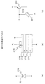
図1は、本発明の実施例1における図6のプリントヘッド13の構成を示す回路図である。
FIG. 1 is a circuit diagram showing the configuration of the
この図1のプリントヘッド13では、駆動装置52を構成するデータ駆動回路60、クロック駆動回路70及び走査回路部100の内、走査回路部100がプリントヘッド13内に配置されているが、データ駆動回路60及びクロック駆動回路70が印刷制御部40内に配置された構成例が示されている。なお、データ駆動回路60及びクロック駆動回路70は、図6に示すように、プリントヘッド13の内部に配置しても良い。
In the
図1に示すプリントヘッド13は、図4中のICチップ13cに形成された走査回路部100及び発光サイリスタアレイ200を有し、これらが複数の接続ケーブル98(=98−1〜98−3)及び複数の接続コネクタ99(=99−1〜99−6)を介して、複数のデータ駆動回路60及びクロック駆動回路70にそれぞれ接続されている。
The
発光サイリスタアレイ200を構成する複数段の発光サイリスタ210(=210−1〜210−n)は、アノードがVCC電源に接続され、カソードが共通端子INを介して接続コネクタ99−4に接続され、ゲートが走査回路部100の各出力端子Q1〜Qnに接続されている。発光サイリスタ210−1〜210−n,・・・の総数は、例えば、A4サイズの用紙に1インチ当たり600ドットの解像度で印刷可能なプリントヘッド13の場合、4992個であり、これらが配列されることになる。
A plurality of light emitting thyristors 210 (= 210-1 to 210-n) constituting the light emitting
走査回路部100は、クロック駆動回路70から第1、第2クロック端子CK1,CK2、接続コネクタ99−2,99−3、接続ケーブル98−2,98−3、及び接続コネクタ99−5,99−6を介して供給される2相の第1及び第2クロックにより駆動され、発光サイリスタアレイ200にトリガ電流を流してオン/オフ動作させる回路であり、複数段の3端子スイッチ素子(例えば、Pゲート型の走査サイリスタ)110(=110−1〜110−n、例えばn=4992)と、複数の第2抵抗120(=120−2〜120−n)と、第2クロック端子CK2から出力される第2クロックを入力するスタート信号用の第1抵抗130と、走査方向決定用の複数段のダイオード140(=140−2〜140−n)と、抵抗151,152とを有し、自己走査型シフトレジスタにより構成されている。
The
各段の走査サイリスタ110(=110−1〜110−n)は、第3端子(例えば、アノード)、第4端子(例えば、カソード)、及び第2制御端子(例えば、ゲート)を有し、アノードが、第1電源としてのVCC電源に接続され、ゲートが、各出力端子Q1〜Qnを介して各段の発光サイリスタ210のゲートに接続されると共に各抵抗120(=120−2〜120−n)を介してグランドGNDに接続されている。但し、初段の走査サイリスタ110−1のゲートとグランドGNDとの間には、抵抗120が設けられていない。
Each stage of the scanning thyristor 110 (= 110-1 to 110-n) has a third terminal (for example, an anode), a fourth terminal (for example, a cathode), and a second control terminal (for example, a gate). The anode is connected to the VCC power supply as the first power supply, the gate is connected to the gate of the
奇数段の走査サイリスタ110−1,110−3,・・・,110−(n−1)のカソードは、抵抗151を介して接続コネクタ99−5に接続されている。偶数段の走査サイリスタ110−2,110−4,・・・,110−nのカソードは、抵抗152を介して接続コネクタ99−6に接続されている。
The cathodes of the odd-numbered scanning thyristors 110-1, 110-3,..., 110- (n−1) are connected to the connection connector 99-5 via the
初段の走査サイリスタ110−1のゲートは、抵抗130を介して接続コネクタ99−6に接続されている。初段から最終段までの各段の走査サイリスタ110−1〜110−nにおけるゲート間は、順方向の各ダイオード140(=140−2〜140−n)を介してそれぞれ接続されている。各ダイオード140は、発光サイリスタ210−1〜210−nが順次点灯する時の走査方向(例えば、図1において右方向)を決定するために設けられている。
The gate of the first-stage scanning thyristor 110-1 is connected to the connection connector 99-6 via the
各段の走査サイリスタ110は、各段の発光サイリスタ210と同様なレイヤ構造を有し、且つ同様な回路動作を行う素子であるが、発光サイリスタ210のような発光機能を必要としないので、上層がメタル膜等の非透光性材料で覆われ、遮光して用いられる。
The
走査回路部100では、クロック駆動回路70の第1及び第2クロック端子CK1,CK2から供給される2相の第1及び第2クロックに基づき、走査サイリスタ110−1〜110−nが択一的にオン状態となり、このオン状態が発光サイリスタアレイ200に伝達され、発光サイリスタ210−1〜210−nの内から発光すべき発光サイリスタ210−1〜210−nを指令する働きをする。この走査回路部100において、オン状態となる各段の走査サイリスタ110のオン状態が、2相の第1及び第2クロック毎に隣接の走査サイリスタ110に伝達され、シフトレジスタと同様の回路動作が行われる構成になっている。
In the
なお、初段の走査サイリスタ110−1においては、2段目以降の走査サイリスク110−2〜110−nと違って、ゲートとグランドGNDとの間を接続する抵抗120が削除されているが、これは部品点数を削減するための工夫であって、低コスト化への配慮が不要である場合には、走査サイリスタ110−1のゲートとグランドGNDとの間に抵抗120を設ける構成とすることもできる。
In the first-stage scanning thyristor 110-1, unlike the second-stage and subsequent scanning thyrists 110-2 to 110-n, the
発光サイリスタアレイ200に接続された複数のデータ駆動回路60は、駆動指令信号である第1制御信号DRVONを生成し、複数の発光サイリスタアレイ200を時分割駆動するためのデータとしての駆動電流Ioutを共通端子INに流す回路である。走査回路部100に接続されたクロック駆動回路70は、第2、第3及び第4の制御信号C1,ST、C2を生成し、走査回路部100に供給するための2相の第1及び第2クロックを出力する回路である。
A plurality of
図1においては、説明を簡略化するために1個のデータ駆動回路60のみが図示されている。複数の発光サイリスタアレイ200は、例えば、総数4992個の発光サイリスタ210−1〜210−n,・・・を有し、これらの発光サイリスタ210−1〜210−n,・・・が複数の発光サイリスタ210−1〜210−nの組にグループ化され、各グループ毎に設けられたデータ駆動回路60によって、それらが同時並行的に分割駆動が行われる構成になっている。
In FIG. 1, only one
一例として典型的な設計例を挙げると、発光サイリスタ210(=210−1〜210−n)を192個配列してアレイ化した発光サイリスタアレイ200のチップを図4中のプリント配線板13b上に26個整列する。これにより、プリントヘッド13に必要な総数4992個の発光サイリスタ210−1〜210−n,・・・を構成している。この際、データ駆動回路60は前記26個の発光サイリスタアレイ200に対応して設けられ、これらのデータ駆動回路60における出力端子の総数は26である。
As a typical design example, a chip of the light emitting
一方、クロック駆動回路70は、アレイ化した走査回路部100のチップを駆動するものであるが、単にクロックを生成するのみならず、後述する走査サイリスタ110の点灯エネルギーを制御する必要があり、プリントヘッド13の高速動作のためには、走査回路部100毎に設けることが好ましい。しかし、プリントヘッド13のデータ転送が低速で良い場合には、クロック駆動回路70の出力端子であるクロック端子CK1,CK2と複数の走査回路部100とを並列に接続することで、その回路を共用することができる。
On the other hand, the
データ駆動回路60は、制御信号DRVONを生成するデータ制御回路61と、その制御信号DRVONを駆動するオープンドレーン形バッファ(例えば、オープンドレーン形インバータ)62と、このオープンドレーン形インバータ62とデータ端子DAとの間に接続された抵抗63とを有している。
The
オープンドレーン形インバータ62は、第1導電形の第1MOSトランジスタ(例えば、PチャネルMOSトランジスタ、以下「PMOS」という。)62aと、制御信号DRVONによりオン/オフ動作する第1スイッチ素子(例えば、第2導電形の第2MOSトランジスタであるNチャネルMOSトランジスタ(以下「NMOS」という。)62bとを有し、これらが第2電源(例えば、3.3Vの電源電圧VDDを出力するVDD電源)とグランドGNDとの間に直列に接続されている。
The
ここで、PMOS62aは、ソース及びゲートが、VDD電源に接続され、ドレーンが、NMOS62bのドレーン及びソースを介してグランドGNDに接続されると共に、抵抗63を介してデータ端子DAに接続され、オフ状態に設定されている。これは、データ駆動回路60が相補形MOSトランジスタ(以下「CMOS」という。)半導体プロセスを用いて製造されるためであって、PMOS62aのドレーン及びサブストレート間に生じる第1整流素子である寄生ダイオードを出力端子の静電気保護素子として用いるためである。
Here, the source and gate of the
例えば、データ制御回路61から出力される制御信号DRVONがLレベルの場合、NMOS62bがオフ状態となり、データ端子DAがハイインピーダンス(以下「Hi−Z」という。)出力状態となる。そのため、共通端子INを介して発光サイリスタ210のカソードがオープンとなってこのカソード電流が遮断されるので、発光サイリスタ210−1〜210−nを全て非発光状態にできる。
For example, when the control signal DRVON output from the
これに対し、制御信号DRVONがHレベルの場合、NMOS62bがオン状態となり、データ端子DA、接続コネクタ99−1、接続ケーブル98−1、接続コネクタ99−4、及び共通端子INを介して、発光サイリスタ210−1〜210−nのカソード電位が略GND電位にまで降下する。これにより、発光サイリスタ210−1〜210−nのアノード・カソード間には、電源電圧VCCと略等しい電圧が印加されることになる。
On the other hand, when the control signal DRVON is at the H level, the
クロック駆動回路70は、第2、第3、第4制御信号C1,ST,C2を生成するクロック制御回路71と、VDD電源により動作し、第2制御信号C1を駆動して第1クロック端子CK1へ出力するオープンドレーン形第1バッファ(例えば、オープンドレーン形インバータ)80と、VDD電源により動作し、第4制御信号C2に基づき、第3制御信号STを駆動して第2クロック端子CK2へ出力するスリーステート形第2バッファ(例えば、スリーステート形出力バッファ)90とを有している。
The
オープンドレーン形インバータ80は、データ駆動回路60中のオープンドレーン形インバータ62と同様の構成である。スリーステート形出力バッファ90は、第4制御信号C2がHレベルの場合、入力される第3制御信号STのHレベル又はLレベルの状態に応じてHレベル又はLレベルに変化する第2クロックを第2クロック端子CK2へ出力し、第4制御信号C2がLレベルの場合、入力される第3制御信号STのHレベル又はLレベルの状態に関わらず、第2クロック端子CK2をHi−Z出力状態にする回路である。
The open
これらのデータ駆動回路60及びクロック駆動回路70に使用されるVDD電源は、発光サイリスタ210及び走査回路部100で使用されるVCC電源とは異なる電圧値(電源電圧VDD<電源電圧VCC)に設定されている。
The VDD power supply used for the data drive
典型的な設計例を挙げると、電源電圧VDDは3.3V、電源電圧VCCは5Vである。これらはいずれも電子回路において標準的に用いられる電源電圧である。しかし、データ駆動回路60やクロック駆動回路70を含む印刷制御部40においては、大規模集積化されたLSI等の素子を含み、半導体微細加工製造プロセスを駆使して製造されるものであって、半導体のスケーリングルールに伴い、その電源電圧値は低くならざるを得ない。これに対し、プリントヘッド13内部に用いられる半導体素子においては、それほどの微細化は必要とされず、十分な耐圧を確保することができる。そのため,データ駆動回路60やクロック駆動回路70の電源電圧VDDを3.3Vとし、サイリスタの電源電圧VCCを5Vとしている。
As a typical design example, the power supply voltage VDD is 3.3V, and the power supply voltage VCC is 5V. These are all power supply voltages used as standard in electronic circuits. However, the
(実施例1の発光サイリスタ)
図7(a)〜(c)は、図1中の発光サイリスタ210を示す構成図である。
(Light Emitting Thyristor of Example 1)
7A to 7C are configuration diagrams showing the light-emitting
図7(a)は、発光サイリスタ210の回路シンボルを示し、アノードA、カソードK、及びゲートGの3つの端子を有している。
FIG. 7A shows a circuit symbol of the
図7(b)は、発光サイリスタ210の断面構造を示す図である。発光サイリスタ210は、例えば、P型GaAsウェハ基材を用い、公知のMO−CVD(Metal Organic-Chemical Vapor Deposition)法により、GaAsウェハ基材の上層に所定の結晶をエピタキシャル成長させることで製造される。
FIG. 7B shows a cross-sectional structure of the
即ち、P型GaAsウェハ基材211の上層に、AlGaAs材料にP型不純物を含ませたP型層212と、N型不純物を含ませ成層したN型層213と、P型不純物を含ませたP型層2144と、N型不純物を含ませ成層したN型層215とを順に積層させたPNPNの4層構造のウェハを形成する。次に、公知のエッチング法を用いて溝部を形成することで、素子分離を行う。又、前記エッチングの過程でP型層214の一部の領域を露出させ、この領域に金属配線を形成してゲートGを形成する。同様に、最上層となるN型層215の一部の領域を露出させ、この領域の一部に金属配線を形成してカソードKを形成する。同様に、P型GaAsウェハ基材211の底面に金属電極を形成して、アノードAを形成する。
That is, a P-
図7(c)は、図7(b)と対比させて描いた発光サイリスタ210の等価回路図である。発光サイリスタ210は、PNPトランジスタ(以下「PNPTR」という。)221とNPNトランジスタ(以下「NPNTR」という。)222とからなり、PNPTR221のエミッタが発光サイリスタ210のアノードAに相当し、NPNTR222のベースが発光サイリスタ210のゲートGに相当し、NPNTR222のエミッタが発光サイリスタ210のカソードKに相当している。又、PNPTR221のコレクタは、NPNTR222のベースに接続され、PNPTR221のベースが、NPNTR222のコレクタに接続されている。
FIG. 7C is an equivalent circuit diagram of the light-emitting
なお、図7に示す発光サイリスタ210では、GaAsウェハ基材上にAlGaAs層を構成したものであるが、これに限定されるものではなく、GaP、GaAsP、AlGaInP、InGaAsPといった材料を用いるものであっても良く、更には、サファイヤ基板上にGaNやAlGaN、InGaNといった材料を成膜したものであっても良い。
In the
(実施例1のプリントヘッドの概略動作)
図1及び図6において、例えば、クロック駆動回路70内のクロック制御回路71から出力される制御信号C1,ST,C2の内、制御信号C1,ST,C2がHレベルになると、インバータ80の出力端子がLレベルになると共に、出力バッファ90がオン状態になってこの出力バッファ90の出力端子がHレベルになる。
(Schematic operation of the print head of Example 1)
1 and 6, for example, when the control signals C1, ST, C2 among the control signals C1, ST, C2 output from the
インバータ80の出力端子のLレベルにより、第1クロック端子CK1、接続コネクタ99−2、接続ケーブル98−2、接続コネクタ99−5、及び抵抗151を介して、初段の走査サイリスタ110−1のカソードがLレベルになる。更に、出力バッファ90の出力端子のHレベルにより、第2クロック端子CK2、接続コネクタ99−3、接続ケーブル98−3、接続コネクタ99−6及び抵抗130を介して、走査サイリスタ110−1のゲートがHレベル(≒電源電圧VCC(5V))になる。これにより、走査サイリスタ110−1がオン状態になる。次いで、CK1、CK2信号に応じて走査回路部100がシフト動作を開始し、次段以降の走査サイリスタ110−2〜110−nのゲートが順にHレベル(≒電源電圧VCC(5V))になって順次オンして行く。
Depending on the L level of the output terminal of the
一方、データ駆動回路60内のデータ制御回路61から出力される制御信号DRVONがLレベルの場合、インバータ62内のNMOS62bがオフ状態となり、データ端子DAがHi−Z出力状態となる。これにより、接続コネクタ99−1、接続ケーブル98−1、接続コネクタ99−4及びプリントヘッド13側の共通端子INを介して、発光サイリスタ210のカソードがオープンとなってこのカソード電流が遮断される。そのため、データ端子DAに流れる駆動電流Ioutがゼロとなり、発光サイリスタ210−1〜210−nが全て非発光状態となる。
On the other hand, when the control signal DRVON output from the
これに対し、データ制御回路61から出力される制御信号DRVONがHレベルの場合、インバータ62内のNMOS62bがオン状態となり、抵抗63を介してデータ端子DAがLレベル(≒GND電位=0V)となる。この結果、接続コネクタ99−1、接続ケーブル98−1及び接続コネクタ99−4を介して共通端子INもLレベル(≒GND電位=0V)となり、各発光サイリスタ210のアノード・カソード間に略電源電圧VCC(≒5V)が印加される。
On the other hand, when the control signal DRVON output from the
この際、発光サイリスタ210−1〜210−nの内、走査回路部100により、発光指令されている発光サイリスタ210のゲートのみが選択的にHレベルにされるので、この発光サイリスタ210のゲート及びカソード間にトリガ電流を生じ、発光指令されている発光サイリスタ210がターンオンすることになる。ターンオンした発光サイリスタ210のカソードに流れる電流は、データ端子DAに流入する電流(即ち、駆動電流Iout)であり、発光サイリスタ210は発光状態となってその駆動電流Ioutの値に応じた発光出力を生じる。
At this time, among the light-emitting thyristors 210-1 to 210-n, only the gate of the light-emitting
(実施例1のプリントヘッドの詳細動作)
図8は、図1のプリントヘッド13の詳細な動作を示すタイミングチャートである。
(Detailed Operation of Printhead of Example 1)
FIG. 8 is a timing chart showing the detailed operation of the
この図8では、図2の画像形成装置1での印刷動作時における1ライン走査において、図1の発光サイリスタ210−1〜210−n(例えば、n=6)を順次点灯させる場合の動作波形が示されている。
In FIG. 8, the operation waveforms when the light emitting thyristors 210-1 to 210-n (for example, n = 6) in FIG. 1 are sequentially turned on in one line scanning during the printing operation in the
本実施例1のように、走査サイリスタ110を用いた走査回路部100の場合、クロック端子CK1,CK2から供給される2相のクロックが用いられ、この2相のクロックは、クロック駆動回路70から出力される。
As in the first embodiment, in the case of the
図8のタイミングチャートにおいて、左端部に示す状態においては、クロック制御回路71から出力される制御信号C1,C2がLレベル、制御信号STがHレベルとなる。これにより、インバータ80の出力側のクロック端子CK1と、出力バッファ90の出力側のクロック端子CK2とは、図8中に破線にて示すHi−Z出力状態となり、奇数段の走査サイリスタ110−1,110−3,・・・の組のカソードと、偶数段の走査サイリスタ110−2,110−4,・・・の組のカソードとがオープンとなり、そのカソード電流が遮断される。そのため、奇数段の走査サイリスタ110−1,110−3,・・・の組と、偶数段の走査サイリスタ110−2,110−4,・・・の組とは、オフ状態になり、走査回路部100における全ての走査サイリスタ110−1〜110−nがオフ状態になる。
In the timing chart of FIG. 8, in the state shown at the left end, the control signals C1 and C2 output from the
又、データ制御回路61から出力される制御信号DRVONはLレベルになっており、インバータ62内のNMOS62bがオフ状態で、このインバータ62の出力端子がHi−Z出力状態である。そのため、共通端子INに接続された発光サイリスタ210−1〜210−nのカソードにおけるカソード電流が遮断され、発光サイリスタ210−1〜210−nもまたオフ状態にある。
Further, the control signal DRVON output from the
その上、走査サイリスタ110−1〜110−n、及び発光サイリスタ210−1〜210−nは無論、抵抗120−2〜120−n,130、及びダイオード140−2〜140−nにも電流を生じないため、図8のタイミングチャートの左端部の状態においては、プリントヘッド13が消費電流が略ゼロの状態にある。その結果、前記プリントヘッド13を用いる画像形成装置1において、印刷休止時に前記論理状態に設定することで、消費電力を低減することが可能となる。以下、
In addition, the scanning thyristors 110-1 to 110-n and the light emitting thyristors 210-1 to 210-n naturally pass current to the resistors 120-2 to 120-n and 130 and the diodes 140-2 to 140-n. Therefore, in the state of the left end portion of the timing chart of FIG. 8, the
(1)1段目走査サイリスタ110−1のターンオン過程
(2)2段目走査サイリスタ110−2のターンオン過程
(3)スタート信号過程(時刻t2)
(4)2段目走査サイリスタ110−2のオン過程(時刻t5)
(5)第1段目発光サイリスタ210−1のオフ状態
について説明する。
(1) Turn-on process of first-stage scanning thyristor 110-1 (2) Turn-on process of second-stage scanning thyristor 110-2 (3) Start signal process (time t2)
(4) ON process of second stage scanning thyristor 110-2 (time t5)
(5) The off state of the first-stage light-emitting thyristor 210-1 will be described.
(1) 1段目走査サイリスタ110−1のターンオン過程
図8の時刻t1において、クロック制御回路71から出力される制御信号C1,ST,C2の内、制御信号C2が立ち上がってHレベルに遷移する。これに伴いクロック端子CK2は、a部に示すように、Hi−Z状態からHレベル状態になる。
(1) Turn-on process of first-stage scanning thyristor 110-1 At time t1 in FIG. 8, among the control signals C1, ST, C2 output from the
時刻t2において、制御信号C1が立ち上がってHレベルに遷移する。これに伴いクロック端子CKlは、b部に示すように、Hi−Z状態からLレベル状態に立ち下がる。この時、クロック端子CK2はHレベルであり、このクロック端子CK2から抵抗130、走査サイリスタ110−1のゲート・カソード間、及び抵抗151を通り、クロック端子CKlに至る経路に電流を生じ、この電流をトリガ電流として走査サイリスタ110−1がターンオンする。
At time t2, the control signal C1 rises and transitions to the H level. Along with this, the clock terminal CKl falls from the Hi-Z state to the L level state as shown in part b. At this time, the clock terminal CK2 is at the H level, and a current is generated from the clock terminal CK2 through the
典型的な設計例では、走査サイリスタ110−1をターンオンさせようとする時のゲート・カソード間電圧は、約1.6Vである。又、クロック駆動回路70の電源電圧VDDは3.3Vであって、前記クロック端子CK2のHレベル電圧は電源電圧VDDと略等しく、走査サイリスタ110−1にゲート電流を生じさせるのに十分な値となっている。
In a typical design example, the gate-cathode voltage when turning on the scanning thyristor 110-1 is about 1.6V. Further, the power supply voltage VDD of the
時刻t3において、データ制御回路61から出力される制御信号DRVONがHレベルに立ち上がると、インバータ62内のNMOS62bがオン状態になり、抵抗63を介してデータ端子DAがLレベルに遷移する。これにより、共通端子INを介して、発光サイリスタ210−1のアノード・カソード間には、電源電圧VCCと略等しい電圧5Vが印加される。
At time t3, when the control signal DRVON output from the
この時、走査サイリスタ110−1がオンしているので、このゲート電位は電源電圧VCC(5V)に略等しい電位にある。走査サイリスタ110−1と発光サイリスタ210−1とはゲート電位を共有しており、このゲート電位が略5Vである。時刻t3でデータ端子DAがLレベルになると、発光サイリスタ210−1のカソード電位もまたLレベル(略0V)であり、このゲート・カソード間に電圧が印加されてゲート電流を生じ、発光サイリスタ210−1がターンオンする。その結果、発光サイリスタ210−1のカソードには、c部に示すように、駆動電流Ioutを生じ、この駆動電流Ioutの値に応じた発光出力を生じる。 At this time, since the scanning thyristor 110-1 is on, the gate potential is substantially equal to the power supply voltage VCC (5V). The scanning thyristor 110-1 and the light emitting thyristor 210-1 share a gate potential, and this gate potential is about 5V. When the data terminal DA becomes L level at time t3, the cathode potential of the light emitting thyristor 210-1 is also L level (approximately 0V), and a voltage is applied between the gate and the cathode to generate a gate current. -1 turns on. As a result, a drive current Iout is generated at the cathode of the light-emitting thyristor 210-1, and a light-emission output corresponding to the value of the drive current Iout is generated as shown in part c.
時刻t4において、制御信号DRVONがLレベルに立ち下がると、インバータ62内のNMOS62bがオフ状態になり、抵抗62を介してデータ端子DAがHi−Z状態に遷移する。後述するように、これにより発光サイリスタ210−1のカソード電流経路が遮断され、この発光サイリスタ210−1がオフして、d部に示すように、駆動電流Ioutが略ゼロとなる。
When the control signal DRVON falls to the L level at time t4, the
本実施例1では、発光サイリスタ210−1を発光させて、図2中の感光体ドラム11上に潜像を形成することができる。この時の露光エネルギー量は、駆動電流Ioutの値に応じて定まる発光パワーと露光時間(=t4−t3)との積である。そのため、発光サイリスタ210−1等に製造ばらつきに起因する発光効率の差があったとしても、前記露光時間を発光サイリスタ210毎に調整することで、露光エネルギー量のばらつきを補正することができる。又、発光サイリスタ210−1を発光させる必要のない場合には、時刻t3〜t4間の制御信号DRVONをLレベルのままとする。このように、制御信号DRVONによって発光サイリスタ210の発光の有無もまた制御することができる。
In the first exemplary embodiment, the light emitting thyristor 210-1 can emit light to form a latent image on the
(2) 2段目走査サイリスタ110−2のターンオン過程
時刻t5において、制御信号STがHレベルからLレベルに立ち下がる。出力バッファ90において制御信号C2がHレベルとなって出力イネーブル状態であるので、時刻t5で出力バッファ90の出力端子がLレベルに遷移し、クロック端子CK2が、e部に示すように、HレベルからLレベルに立ち下がる。この時、走査サイリスタ110−1はオン状態にあり、このゲートがHレベルとなっている。走査サイリスタ110−1のゲートのHレベルは、ダイオード140−2によって走査サイリスタ110−2のゲートに伝達され、このゲート・カソード間を通り、抵抗152を介してクロック端子CK2に流入するゲート電流を生じる。この結果、走査サイリスタ110−2がターンオンする。
(2) Turn-on process of second stage scanning thyristor 110-2 At time t5, the control signal ST falls from the H level to the L level. Since the control signal C2 becomes H level in the
時刻t6において、制御信号ClがLレベルに立ち下がり、f部に示すように、クロック端子CK1はHi−Z状態になる。これにより、走査サイリスタ110−1のカソード電流の経路は遮断され、走査サイリスタ110−1がターンオフする。 At time t6, the control signal Cl falls to the L level, and the clock terminal CK1 enters the Hi-Z state as shown in the f section. Thereby, the path of the cathode current of the scanning thyristor 110-1 is cut off, and the scanning thyristor 110-1 is turned off.
時刻t7において、制御信号DRVONがHレベルに立ち上がり、インバータ62内のNMOS62bがオン状態になり、抵抗63を介してデータ端子DAはLレベルに遷移する。データ端子DAがLレベルに遷移すると、共通端子INを介して発光サイリスタ210−2のアノード・カソード間には、電源電圧VCCと略等しい電圧が印加される。この時、走査サイリスタ110−2はオン状態、走査サイリスタ110−1はオフ状態になっている。このように、走査サイリスタ110−2はオンしているので、この走査サイリスタ110−2のゲートに対してゲート電位を共有している発光サイリスタ210−2がオンして、このカソードには、g部に示すように、駆動電流Ioutを生じ、この駆動電流Ioutの値に応じた発光出力を生じる。
At time t7, the control signal DRVON rises to H level, the
時刻t8において、制御信号DRVONがLレベルに立ち下がり、インバータ62内のNMOS62bがオフし、抵抗63を介してデータ端子DAがHi−Z状態に遷移する。これにより、共通端子INを介して、発光サイリスタ210−2におけるカソード電流経路が遮断され、発光サイリスタ210−2はオフして、h部に示すように、駆動電流Ioutが略ゼロとなる。
At time t8, the control signal DRVON falls to L level, the
時刻t9において、制御信号C1がHレベルに立ち上がり、i部に示すように、クロック端子CK1はHi−Z状態からLレベルに遷移する。この時,走査サイリスタ110−2はオン状態にあり、このゲートがHレベルとなっている。このHレベルは、ダイオード140−3によって走査サイリスタ110−3のゲートに伝達され、このゲート・カソード間を通り、抵抗151を介してクロック端子CK1に流入するゲート電流を生じる。この結果、走査サイリスタ110−3がターンオンする。
At time t9, the control signal C1 rises to the H level, and the clock terminal CK1 transitions from the Hi-Z state to the L level as shown in the i section. At this time, the scanning thyristor 110-2 is in the ON state, and this gate is at the H level. This H level is transmitted to the gate of the scanning thyristor 110-3 by the diode 140-3, and generates a gate current that flows between the gate and the cathode and flows into the clock terminal CK1 through the
時刻t10において、制御信号C2がLレベルになる。この時、制御信号STはLレベルになっており、制御信号C2がLレベルとされることで、出力バッファ90の出力端子はHi−Z状態になる。この結果、j部に示すように、クロック端子CK2はHi−Z状態になり、抵抗152を介して走査サイリスタ110−2のカソード電流経路が遮断され、この走査サイリスタ110−2がターンオフする。
At time t10, the control signal C2 becomes L level. At this time, the control signal ST is at the L level, and when the control signal C2 is set to the L level, the output terminal of the
以下同様に、制御信号C1,C2の遷移と制御信号DRVONのオン/オフとが順に発生し、走査サイリスタ110−3〜10−nが順次点灯する。 Similarly, the transition of the control signals C1 and C2 and the on / off of the control signal DRVON occur in order, and the scanning thyristors 110-3 to 10-n are sequentially turned on.
(3) スタート信号過程(時刻t2)
図9−1は、図8の時刻t2における図1の詳細動作を説明するための要部の回路図である。この図9−1では、クロック駆動回路70内の要部構成と、走査回路部100内の一例として走査サイリスタ110−1,110−2を抜き出して周辺回路との関係を説明する図が示されている。
(3) Start signal process (time t2)
FIG. 9A is a circuit diagram of the main part for explaining the detailed operation of FIG. 1 at time t2 of FIG. FIG. 9A is a diagram illustrating the configuration of the main part in the
クロック駆動回路70において、第1バッファであるオープンドレーン形インバータ80は、第2電源であるVDD電源と第1クロック端子CK1との間に接続された第1導電形のMOSトランジスタ(例えば、PMOS)81と、第1クロック端子CK1とグランドGNDとの間に接続され、第2制御信号C1に基づきオン/オフ動作する第2スイッチ素子(例えば、第2導電形のMOSトランジスタであるNMOS)82と、VDD電源と第1クロック端子CK1との間に逆方向に接続された第2整流素子(例えば、第2ダイオード)81aと、第1クロック端子CK1とグランドGNDとの間に逆方向に接続された整流素子(例えば、ダイオード)82aとを有している。
In the
ここで、PMOS81は、ソース及びゲートがVDD電源に接続され、図示しないサブストレートがVDD電源に接続され、ドレーンが第1クロック端子CK1に接続され、常時オフ状態になっている。NMOS82は、ドレーンが第1クロック端子CK1に接続され、ゲートに第2制御信号C1が入力され、ソースがグランドGNDに接続されている。ダイオード81aは、PMOS81のドレーン・サブストレート間に生じる寄生ダイオードであり、アノードが第1クロック端子CK1に接続され、カソードがVDD電源(3.3V)に接続されている。又、ダイオード82aは、NMOS82のドレーン・サブストレート間に生じる寄生ダイオードである。
Here, the source and gate of the
なお、ダイオード81aは、通常のダイオード素子で構成しても良く、この場合はPMOS81が動作上不要となるので省略しても良い。又、ダイオード82aは、NMOS82により生じる寄生ダイオードであり、動作上は不要である。
The
第2バッファであるスリーステート形出力バッファ90は、第4制御信号C2を反転するインバータ91と、第4制御信号C2と第3制御信号STとの否定論理積を求める2入力の否定論理積回路(以下「NAND回路」という。)92と、インバータ91の出力信号と第3制御信号STとの否定論理和を求める2入力の否定論理和回路(以下「NOR回路」という。)93と、第2電源であるVDD電源(3.3V)と第2クロック端子CK2との間に接続され、NAND回路92の出力信号によりオン/オフ動作する第1導電形の第3スイッチ素子(例えば、PMOS)94と、第2クロック端子CK2とグランドGNDとの間に接続され、NOR回路93の出力信号によりオン/オフ動作する第2導電形の第4スイッチ素子(例えば、MMOS)95と、VDD電源と第2クロック端子CK2との間に逆方向に接続された第3整流素子(例えば、第3ダイオード)94aと、第2クロック端子CK2とグランドGNDとの間に逆方向に接続された整流素子(例えば、ダイオード)95aとを有している。
The three-
ここで、PMOS94は、ソースがVDD電源に接続され、ゲートがNAND回路92の出力端子に接続され、ドレーンが第2クロック端子CK2に接続されている。NMOS95は、ドレーンが第2クロック端子CK2に接続され、ゲートがNOR回路93の出力端子に接続され、ソースがグランドGNDに接続されている。ダイオード94aは、PMOS94のドレーン・サブストレート間に生じる寄生ダイオードであり、アノードが第2クロック端子CK2に接続され、カソードがVDD電源(3.3V)に接続されている。又、ダイオード95aは、NMOS95のドレーン・サブストレート間に生じる寄生ダイオードである。
Here, the
なお、ダイオード94aは、通常のダイオード素子で構成しても良い。又、ダイオード95aは、NMOS95により生じる寄生ダイオードであり、動作上は不要である。
The
このような構成において、オープンドレーン形インバータ80は、図1中のオープンドレーン形インバータ62と同様の動作を行う。これに対し、スリーステート形出力バッファ90は、次のような動作を行う。
In such a configuration, the open
PMOS94及びNMOS95のゲートを共にHレベルとする時、PMOS94はオフ状態、NMOS95はオン状態となって、クロック端子CK2がLレベルとなる。これに対し、PMOS94及びNMOS95のゲートを共にLレベルとする時、PMOS94はオン状態、NMOS95はオフ状態となって、クロック端子CK2がHレベルとなる。更に、PMOS94のゲートをHレベル、NMOS95のゲートをLレベルにする時、PMOS94及びNMOS95が共にオフ状態となって、クロック端子CK2がHi−Z出力状態となる。
When both the gates of the
このように、出力バッファ90は、HレベルとLレベルの他に、Hi−Z出力状態を備えており、この3つの出力状態は、出力バッファ90に入力される第4の制御信号C2と第3の制御信号STとの組み合わせに応じて、インバータ91、NAND回路92及びNOR回路93の働きにより、PMOS94及びNMOS95のゲート信号を発生させることで行われる。
As described above, the
図9−1における破線矢印は、図8のタイミングチャートにおける時刻t2の直後の状態における電流経路を示している。 A broken line arrow in FIG. 9-1 indicates a current path in a state immediately after time t2 in the timing chart of FIG.
この状態においては、制御信号C1はHレベルとなっており、インバータ80内のNMOS82がオン状態になる。PMOS81は常にオフ状態であるので、クロック端子CK1がLレベルとなる。又、制御信号C2,STがHレベルとなっており、PMOS94はオン状態、NMOS95はオフ状態となり、クロック端子CK2がHレベルとなってVDD電源(3.3V)に略等しい出力電位となる。
In this state, the control signal C1 is at the H level, and the
これにより、VDD電源(3.3V)から、PMOS94を通り、クロック端子CK2、抵抗130、走査サイリスタ110−1のゲート・カソード間、抵抗151、クロック端子CK1、及びNMOS82を経由してグランドGNDへ至る経路で電流が流れる。この時、走査サイリスタ110−1のゲート・カソード間に生じる順電圧Vgkは、典型的な設計例では約1.6Vであって、走査サイリスタ110−1のゲートには、これをオンさせるに十分なゲート電流を生じさせることができる。この結果、走査サイリスタ110−1はターンオンする。
As a result, the VDD power supply (3.3 V) passes through the
(4) 走査サイリスタ110−2のオン過程(時刻t5)
図9−2は、図8の時刻t5における図1の詳細動作を説明するための要部の回路図であり、図9−1中の要素と共通の要素には共通の符号が付されている。
(4) On-process of scanning thyristor 110-2 (time t5)
FIG. 9-2 is a circuit diagram of a main part for explaining the detailed operation of FIG. 1 at time t5 in FIG. 8. Elements common to those in FIG. 9-1 are denoted by common reference numerals. Yes.
図9−2中の破線矢印は、図8のタイミングチャートにおける時刻t5の直後の状態における電流経路を示している。 A broken line arrow in FIG. 9B indicates a current path in a state immediately after time t5 in the timing chart of FIG.
この状態においては、制御信号C1はHレベルになっており、NMOS82がオン状態になる。PMOS81は常にオフ状態であるので、クロック端子CK1がLレベルとなる。又、制御信号C2はHレベルとなっており、制御信号STは時刻t4でLレベルに立ち下がる。これにより、NAND回路92の出力信号を入力するPMOS94のゲートはHレベルとなり、このPMOS94がオフ状態になる。
In this state, the control signal C1 is at the H level, and the
これと同時に、NOR回路93の出力信号を入力するNMOS95のゲートはHレベルとなり、このNMOS95がオン状態になる。この結果、図8のe部に示すように、クロック端子CK2はLレベルになる。
At the same time, the gate of the
図9−1を用いて説明したように、時刻t2の直後に走査サイリスタ110−1はターンオンしており、図9−2中の一点鎖線矢印で示すように、VCC電源から走査サイリスタ110−1のアノード・カソード間、抵抗151、クロック端子CK1及びNMOS82を経由してグランドGNDに至る経路に電流を生じている。この時、走査サイリスタ110−1のゲート電位はVCC電源(5V)に略等しい電位となっており、クロック端子CK2がLレベルに遷移したことで、図9−2中の破線矢印で示すように、走査サイリスタ110−1のゲート、ダイオード140−2、走査サイリスタ110−2のゲート・カソード間、抵抗152、クロック端子CK2及びNMOS95を経由してグランドGNDに至る経路に電流を生じる。
As described with reference to FIG. 9A, the scanning thyristor 110-1 is turned on immediately after the time t2, and the scanning thyristor 110-1 is supplied from the VCC power source as indicated by a one-dot chain line arrow in FIG. A current is generated in a path extending from the anode to the cathode, through the
ダイオード140−2の順電圧をVf、走査サイリスタ110−2のゲート・カソード間順電圧をVgkとする時、前記破線矢印の経路に電流を生じさせるためには、
Vf+Vgk<VCC
であることを要する。典型的例では、Vf=1.6V、Vgk=1.6Vであるので、VCC電源を5Vとする場合には、破線矢印の経路には十分な電流値を確保することができる。
When the forward voltage of the diode 140-2 is Vf and the forward voltage between the gate and cathode of the scanning thyristor 110-2 is Vgk, in order to generate a current in the path of the broken line arrow,
Vf + Vgk <VCC
It is necessary to be. In a typical example, Vf = 1.6V and Vgk = 1.6V. Therefore, when the VCC power supply is set to 5V, a sufficient current value can be secured in the path indicated by the broken-line arrow.
(5) 発光サイリスタ210−1のオフ状態
図9−3は、図1の発光サイリスタ210−1におけるオフ状態への遷移動作を説明するための要部の回路図であり、図9−1及び図9−2中の要素と共通の要素には共通の符号が付されている。
(5) OFF State of Light-Emitting Thyristor 210-1 FIG. 9-3 is a circuit diagram of the main part for explaining the transition operation to the OFF state in the light-emitting thyristor 210-1 of FIG. Elements common to the elements in FIG. 9B are denoted by common reference numerals.
図9−3では、図1中の走査回路部100内の走査サイリスタ110−1,110−2と、発光サイリスタアレイ200内の発光サイリスタ210−1,210−2と、データ駆動回路60と、クロック駆動回路70内のオープンドレーン形インバータ80とを抜き出して図示している。この図9−3を用いて、光サイリスタ210−1のオフ指令状態においてこの光サイリスタ210−1の確実なオフが可能となることを説明する。
9-3, the scanning thyristors 110-1 and 110-2 in the
オープンドレーン形インバータ62は、第2電源であるVDD電源とインバータ出力端子との間に接続された第1導電形のMOSトランジスタ(例えば、PMOS)62aと、インバータ出力端子とグランドGNDとの間に接続され、第1制御信号DRVONに基づきオン/オフ動作する第1スイッチ素子(例えば、第2導電形のMOSトランジスタであるNMOS)62aと、図1では図示を省略されているが、VDD電源とインバータ出力端子との間に逆方向に接続された第1整流素子(例えば、第1ダイオード)64と、図1では図示を省略されているが、インバータ出力端子とグランドGNDとの間に逆方向に接続された整流素子(例えば、ダイオード)65とを有している。
The
ここで、PMOS62aは、ソース及びゲートがVDD電源に接続され、図示しないサブストレートがVDD電源に接続され、ドレーンがインバータ出力端子に接続され、常時オフ状態になっている。NMOS62bは、ドレーンがインバータ出力端子に接続され、ゲートに第1制御信号DRVONが入力され、ソースがグランドGNDに接続されている。ダイオード64は、PMOS62aのドレーン・サブストレート間に生じる寄生ダイオードであり、アノードがインバータ出力端子に接続され、カソードがVDD電源に接続されている。又、ダイオード65は、NMOS62bのドレーン・サブストレート間に生じる寄生ダイオードである。
Here, the source and gate of the
なお、ダイオード64は、通常のダイオード素子で構成しても良く、この場合はPMOS62aが動作上不要となるので省略しても良い。又、ダイオード65は、NMOS62bにより生じる寄生ダイオードであり、動作上は不要である。
The
例えば、走査回路部100及び発光サイリスタアレイ200のVCC電源は5Vに設定され、データ駆動回路60及びクロック駆動回路70のVCC電源は3.3Vに設定されている。
For example, the VCC power supply of the
図9−3において、発光サイリスタ210に対するオフ指令時の動作を考える。これは、図8のタイミングチャートにおいて、時刻t3〜t6等の時刻t2以前等の状態に相当するものである。
In FIG. 9C, consider the operation at the time of turning off the
この際、データ駆動回路60のインバータ62とクロック駆動回路70のインバータ80とは同一構成であるため、一例としてデータ駆動回路60内のインバータ62と発光サイリスタ210−1の動作を考えることとする。
At this time, since the
発光サイリスタ210−1のオフ指令状態においては、制御信号DRVONがLレベルとされ、インバータ62内のNMOS62bがオフ状態になっている。この時、PMOS62aのゲートはVDD電源に接続されており、オフ状態である。
In the off command state of the light emitting thyristor 210-1, the control signal DRVON is at the L level, and the
図9−3において、破線矢印で示す電流経路を考えると、VCC電源(5V)から、発光サイリスタ210−1のアノード・カソード間、抵抗63及びダイオード64を経由してVDD電源(3.3V)となる経路をとる。発光サイリスタ210−1がオンするには、このアノード・カソード間電圧をVak、ダイオード64の順電圧をVf(シリコンSiの場合)とする時、破線矢印の経路に電流が流れるためには、
Vak+Vf<VCC−VDD (1)
となる必要がある。しかし、典型的な設計例では、
Vak=1.6V、Vf(Si)=0.6V
であり、
VCC−VDD=5V−3.3V=1.7V
である。そのため、前記(1)式を満たすことはなく、破線矢印の経路には電流を生じないことが判る。
9-3, when considering the current path indicated by the broken line arrow, the VDD power supply (3.3 V) is supplied from the VCC power supply (5 V) via the
Vak + Vf <VCC−VDD (1)
It is necessary to become. But in a typical design example,
Vak = 1.6V, Vf (Si) = 0.6V
And
VCC-VDD = 5V-3.3V = 1.7V
It is. Therefore, it can be seen that the equation (1) is not satisfied and no current is generated in the path indicated by the broken arrow.
従って、図9−3(図1)の構成において、印刷制御部40が発光サイリスタ210及び走査サイリスタ110のオフ指令をしている時、発光サイリスタ210−1〜210−n、及び走査サイリスタ110−1〜110−nは、確実にオフ状態を維持することになる。
Therefore, in the configuration of FIG. 9-3 (FIG. 1), when the
前記の構成は、インバータ62をオープンドレーン形式としたことによる効果によるものである。
The above-described configuration is due to the effect obtained by making the
これを明確にするため、別の構成として、インバータ62をCMOSプッシュプル形インバータとする場合の動作を思考実験してみる。
In order to clarify this, as another configuration, a thought experiment is performed on the operation when the
インバータ62をCMOSプッシュプル構成とするためには、PMOS62aのゲートをNMOS62bのゲートに接続すれば良い。
In order to make the
前述したケースと同様に、制御信号DRVONがLレベルの場合を考えると、NMOS62bがオフ状態であり、PMOS62aのゲートもLレベルとされるので、このPMOS62aはオン状態となる。この時、電流経路は一点鎖線矢印で示すようになり、VCC電源(5V)から発光サイリスタ210−1のアノード・カソード間、抵抗63、及びPMOS62aを経由してVDD電源(3.3V)の経路を通るものとなる
As in the case described above, considering the case where the control signal DRVON is at the L level, the
この時、PMOS62aがオン状態にあって、このドレーン・ソース間電圧は無視できるほど小さい。そのため、一点鎖線矢印の経路に電流が流れるためには、
Vak<VCC−VDD (2)
となる必要がある。ところが、典型的な設計例ではVak=1.6Vであり、
VCC−VDD=5V−3.3V=1.7V
であるため、前記(2)式を満たすことになって、一点鎖線矢印の経路には電流を生じる可能性がある。この結果、従来のデータ駆動回路のままで発光サイリスタ210−1〜210−nのアノード電圧(VCC)を5Vとする場合においては、一度オン状態となった発光サイリスタ210のカソード電流を遮断することができないことになって、確実なオフ動作を実現できないことが判る。
At this time, the
Vak <VCC-VDD (2)
It is necessary to become. However, in a typical design example, Vak = 1.6V,
VCC-VDD = 5V-3.3V = 1.7V
Therefore, the above equation (2) is satisfied, and a current may be generated in the path indicated by the alternate long and short dash line. As a result, when the anode voltage (VCC) of the light emitting thyristors 210-1 to 210-n is set to 5 V with the conventional data driving circuit, the cathode current of the
これに対し、本実施例1における図1及び図9−3の構成においては、PMOS62aがオフ状態とされ、図9−3に示す一点鎖線矢印の電流経路を、破線矢印経路に変更することができ、前述したように、ダイオード64の順電圧(約0.6V)の効果により、破線矢印で示す経路に電流が流れないようにすることができる。
On the other hand, in the configuration of FIG. 1 and FIG. 9-3 in the first embodiment, the
(実施例1の効果)
本実施例1によれば、次の(a)〜(d)のような効果がある。
(Effect of Example 1)
According to the first embodiment, there are the following effects (a) to (d).
(a) 従来構成の走査回路部の駆動においては、例えば、図1のクロック駆動回路70の出力側にCR微分回路をそれぞれ設けてアンダシュート波形を生成し、2個のクロック端子CK1,CK2から2相のクロックを出力している。この際、CR微分回路においては、直流成分を伝達することができないので、2個のクロック端子CK1,CK2に対して各2個の出力端子(=合計4個の出力端子)、即ち、転送クロック当たり2個で合計4個の出力端子が必要であった。
(A) In driving the scanning circuit unit of the conventional configuration, for example, a CR differentiating circuit is provided on the output side of the
これに対し、本実施例1によれば、図1のような回路構成にすることにより、クロック駆動回路70におけるクロック端子数が転送クロック当たり1個で良く、従来構成と比べて所要端子の数を半減することができる。更に、従来構成のクロック駆動回路に備えていたキャパシタ等の外付け部品が不要になる。これにより、プリントヘッド13におけるデータ転送速度を向上できることは勿論のこと、クロック駆動回路70のクロック端子数の減少によって、回路規模の削減と、これによる低コスト化も期待できる。
On the other hand, according to the first embodiment, by adopting the circuit configuration as shown in FIG. 1, the number of clock terminals in the
(b) データ駆動用及びクロック駆動用のVDD電源(例えば、3.3V)のバッファをオープンドレーン形インバータ62,80にし、発光サイリスタ210及び走査サイリスタ110のアノード電源をVCC電源(例えば、5V)にしている。これにより、発光サイリスタ210と走査サイリスタ110のオフ時には、これらの電流経路にインバータ62,80中のPMOS寄生ダイオード64,81aが介在するため、発光サイリスタ210と走査サイリスタ110が誤ってターンオンすることはない。
(B) The VDD power source (for example, 3.3V) buffer for data driving and clock driving is made into the open
(c) 初段の走査サイリスタ110−1のゲートと第2クロック端子CK2とを、抵抗130にて接続しているので、スタート信号が不要になる。更に、データ駆動回路60及びクロック駆動回路70は、VDD電源(例えば、3.3V)で動作し、その出力部にオープンドレーン形インバータ62,80を設け、発光サイリスタ210と走査サイリスタ110のアノード電源としてVCC電源(例えば、5V)を使用している。これにより、電源電圧として一般的な3.3VのVDD電源によりプリントヘッド駆動を行うことができる。
(C) Since the gate of the first-stage scanning thyristor 110-1 and the second clock terminal CK2 are connected by the
(d) 本実施例1の画像形成装置1によれば、プリントヘッド13を採用しているので、スペース効率及び光取り出し効率に優れた高品質の画像形成装置1を提供することができる。即ち、プリントヘッド13を用いることにより、本実施例1のフルカラーの画像形成装置1に限らず、モノクロ、マルチカラーの画像形成装置においても効果が得られるが、特に、露光装置としてのプリントヘッド13を数多く必要とするフルカラーの画像形成装置1において一層大きな効果が得られる。
(D) According to the
本発明の実施例2における画像形成装置1では、主としてプリントヘッド13Aの回路構成が、実施例1のプリントヘッド13と異なるので、以下、その異なる部分について説明する。
In the
(実施例2のプリントヘッド)
図10は、本発明の実施例2におけるプリントヘッド13Aの構成を示回路図であり、実施例1を示す図1中の要素と共通の要素には共通の符号が付されている。
(Print head of Example 2)
FIG. 10 is a circuit diagram showing the configuration of the print head 13A according to the second embodiment of the present invention. Elements common to those in FIG. 1 showing the first embodiment are denoted by common reference numerals.
本実施例2のプリントヘッド13Aは、実施例1の走査回路部100及び発光サイリスタアレイ200とは異なる構成の走査回路部100A及び発光サイリスタアレイ200Aを有し、これらが実施例1と同様の複数の接続ケーブル98(=98−1〜98−3)及び複数の接続コネクタ99(=99−1〜99−6)を介して、実施例1の印刷制御部40とは異なる構成の印刷制御部40Aに接続されている。走査回路部100A及び発光サイリスタアレイ200Aは、VDD電源(例えば、3.3V)により動作する構成になっている。
The print head 13A according to the second embodiment includes a scanning circuit section 100A and a light emitting
印刷制御部40Aは、実施例1のデータ駆動回路60及びクロック駆動回路70とは異なる構成の第1駆動回路(例えば、データ駆動回路)60A及び第2駆動回路(例えば、クロック駆動回路)70Aを有している。データ駆動回路60Aは、VDD電源により動作して発光サイリスタアレイ200A側の共通端子INをH/Lレベルに駆動する回路である。クロック駆動回路70Aは、VDD電源により動作して走査回路部100Aを駆動するための2相の第1及び第2クロックを出力する回路である。
The print controller 40A includes a first drive circuit (for example, a data drive circuit) 60A and a second drive circuit (for example, a clock drive circuit) 70A having configurations different from those of the data drive
本実施例2において、発光サイリスタアレイ200Aを駆動する駆動装置は、実施例1と同様に、走査回路部100A、データ駆動回路60A、及びクロック駆動回路70Aを有している。図10では、データ駆動回路60A及びクロック駆動回路70Aが印刷制御部40A内に配置された構成例が示されているが、実施例1の図6と同様に、データ駆動回路60A及びクロック駆動回路70Aをプリントヘッド13A内に配置しても良い。
In the second embodiment, the driving device for driving the light emitting
走査回路部100Aにより走査される発光サイリスタアレイ200Aは、実施例1と略同様に、3端子発光素子としての例えば複数段のPゲート型発光サイリスタ210A(=210A−1〜210A−n,・・・)を有し、これらの各発光サイリスタ210Aの第1端子(例えば、アノード)がVDD電源に接続され、第2端子(例えば、カソード)が駆動電流Ioutを流す共通端子INを介して接続コネクタ99−4に接続され、第1制御端子(例えば、ゲート)が走査回路部100Aの各出力端子Q1〜Qnに接続されている。発光サイリスタ210A−1〜210A−n,・・・の総数は、実施離1と同様に、例えば、A4サイズの用紙に1インチ当たり600ドットの解像度で印刷可能なプリントヘッド13Aの場合、4992個であり、これらが配列されることになる。
The light emitting
走査回路部100Aは、クロック駆動回路70Aから第1、第2クロック端子CK1,CK2、接続コネクタ99−2,99−3、接続ケーブル98−2,98−3、及び接続コネクタ99−5,99−6を介して供給される2相の第1及び第2クロックにより駆動され、発光サイリスタアレイ200Aにトリガ電流を流してオン/オフ動作させる回路である。この走査回路部100Aは、実施例1の構成とは異なり、複数段の4端子スイッチ素子(例えば、Nゲート及びPゲートの2つの制御端子を有する4端子走査サイリスタ)110A(=110A−1〜110A−n、例えばn=4992)と、第2クロック端子CK2から出力される第2クロックを入力するスタート信号用の第1抵抗130と、抵抗151,152と、走査方向決定用の複数段のインバータ160(=160−1〜160−(n−1))とを有し、自己走査型シフトレジスタにより構成されている。最終段のインバータ160−nは、走査方向の決定が不要であるから、設けられていない。
The scanning circuit unit 100A includes first and second clock terminals CK1 and CK2, connection connectors 99-2 and 99-3, connection cables 98-2 and 98-3, and connection connectors 99-5 and 99 from the clock driving circuit 70A. This circuit is driven by the two-phase first and second clocks supplied via -6, and causes a trigger current to flow through the light-emitting
各段の走査サイリスタ110A(=110A−1〜110A−n)は、第3端子(例えば、アノード)、第4端子(例えば、カソード)、第2制御端子(例えば、第1ゲート)G1、及び第3制御端子(例えば、第2ゲート)G2を有し、アノードが、VDD電源に接続され、第2ゲートG2が、各出力端子Q1〜Qnを介して各段の発光サイリスタ210Aのゲートに接続されている。
The
奇数段の走査サイリスタ110A−1,110A−3,・・・,110A−(n−1)のカソードは、抵抗151を介して接続コネクタ99−5に接続されている。偶数段の走査サイリスタ110A−2,110A−4,・・・,110A−nのカソードは、抵抗152を介して接続コネクタ99−6に接続されている。初段の走査サイリスタ110A−1の第2ゲートは、抵抗130を介して接続コネクタ99−6に接続されている。
The cathodes of the odd-numbered
初段から最終段までの各段の走査サイリスタ110A−1〜110A−nにおける第1ゲートG1及び第2ゲートG2間は、順方向の各段のインバータ160(=160−1〜160−(n−1))を介してそれぞれ接続されている。即ち、前段の走査サイリスタ(例えば、110A−1)の第2ゲートG2と、後段の走査サイリスタ(例えば、110A−2)の第1ゲートG1との間は、順方向のインバータ(例えば、160−1)を介して接続されている。
Between the first gate G1 and the second gate G2 in the
各段のインバータ160(=160−1〜160−(n−1))は、発光サイリスタ210A−1〜210A−nが順次点灯する時の走査方向(例えば、図10において右方向)を決定するために設けられており、バイポーラトランジスタである各NPNTR161(=161−1〜161−(n−1))と、第2抵抗としての各負荷抵抗162(=162−1〜162−(n−1))とによりそれぞれ構成されている。各段のインバータ160(例えば、160−1)において、NPNTR161(例えば、161−1)は、ベースが前段の走査サイリスタ110A(例えば、110A−1)の第2ゲートG2に接続され、コレクタが負荷抵抗162(例えば、162−1)を介してVDD電源に接続されると共に後段の走査サイリスタ110A(例えば、110A−2)の第1ゲートG1に接続され、エミッタが前段の走査サイリスタ110A(例えば、110A−1)のカソードに接続されている。
Each stage of inverter 160 (= 160-1 to 160- (n−1)) determines the scanning direction (for example, the right direction in FIG. 10) when the
各段の走査サイリスタ110Aは、各段の発光サイリスタ210Aと同様なレイヤ構造を有し、且つ同様な回路動作を行う素子であるが、発光サイリスタ210Aのような発光機能を必要としないので、上層がメタル膜等の非透光性材料で覆われ、遮光して用いられる。
The
走査回路部100Aでは、実施例1と略同様に、クロック駆動回路70Aの第1及び第2クロック端子CK1,CK2から供給される2相の第1及び第2クロックに基づき、走査サイリスタ110A−1〜110A−nが択一的にオン状態となり、このオン状態が発光サイリスタアレイ200Aに伝達され、発光サイリスタ210A−1〜210A−nの内から発光すべき発光サイリスタ210A−1〜210A−nを指令する働きをする。この走査回路部100Aにおいて、オン状態となる各段の走査サイリスタ110Aのオン状態が、2相の第1及び第2クロック毎に隣接の走査サイリスタ110Aに伝達され、シフトレジスタと同様の回路動作が行われる構成になっている。
In the scanning circuit unit 100A, similar to the first embodiment, the
このような走査回路部100Aでは、図1に示す実施例1の走査回路部100に対して以下のような相違点がある。
Such a scanning circuit unit 100A has the following differences from the
実施例1の走査回路部100においては、走査サイリスタ110(=110−1〜110−n)として三端子サイリスタが用いられ、各段の走査サイリスタ110のゲート間がダイオード140によりそれぞれ接続されている。
In the
このような構成を採用している理由は、走査サイリスタ110のターンオン過程において、ゲートが入力端子として機能し、この走査サイリスタ110がオンした後には、ゲートが出力端子として振る舞う特性を備えている。そのため、各段の走査サイリスタ110を順次オンさせようとする時、転送方向(例えば、図1において右方向)を決定させる必要があるからである。
The reason for adopting such a configuration is that the gate functions as an input terminal in the turn-on process of the
しかし、実施例1の走査回路部100において、走査サイリスタ110のゲート間をダイオード140を用いて接続することで、転送方向を規制する効果が得られたが、ゲートトリガ電流の流れる経路中に、ダイオード140と走査サイリスタ110のゲート・カソード間の順方向電圧がそれぞれ含まれることになってしまい、両者電圧の加算値が電源電圧VDDに略等しくなって、3.3Vといった通常用いられるVDD電源では、ゲートトリガ電流を生じさせることができなくなる。
However, in the
そこで、このような不都合を解消するために、本実施例2の走査回路部100Aでは、実施例1の3端子の走査サイリスタ110に新たなゲートを設けた4端子の走査サイリスタ110Aを用い、正論理の他、負論理の制御信号を受け付けることを可能としている。
Therefore, in order to eliminate such inconvenience, the scanning circuit unit 100A of the second embodiment uses a four-
即ち、走査サイリスタ110Aの第1ゲートG1を負論理の入力端子として機能させ、第2ゲートG2を正論理のデータ出力端子として動作させ、NPNTR161と負荷抵抗162とでインバータ160を構成して、前段の走査サイリスタ110Aの第2ゲートG2から出力される正論理のデータをインバータ160で反転し、負論理のデータを後段の走査サイリスタ110Aの第1ゲートG1に入力している。このようにすることで、インバータ160の入出力信号の伝達方向が一方向に規制されることになるので、後段の走査サイリスタ110A(例えば、110A−2)から前段の走査サイリスタ110A(例えば、110A−1)方向へ、逆方向に転送される誤動作を防ぐことができる。
That is, the first gate G1 of the
前記発光サイリスタアレイ200Aに接続された複数のデータ駆動回路60Aは、実施例1のデータ駆動回路60と略同様に、駆動指令信号である第1制御信号DRVONを生成し、複数の発光サイリスタアレイ200Aを時分割駆動するためのデータとしての駆動電流Ioutを共通端子INに流す回路である。走査回路部100Aに接続されたクロック駆動回路70Aは、実施例1のクロック駆動回路70とは異なり、第2、第4制御信号C1,C2を生成し、走査回路部100Aに供給するための2相の第1及び第2クロックを出力する回路である。
The plurality of data driving circuits 60A connected to the light emitting
図10においては、実施例1の図1と同様に、説明を簡略化するために1個のデータ駆動回路60Aのみが図示されている。複数の発光サイリスタアレイ200Aは、例えば、総数4992個の発光サイリスタ210A−1〜210A−n,・・・を有し、これらの発光サイリスタ210A−1〜210A−n,・・・が複数の発光サイリスタ210A−1〜210A−nの組にグループ化され、各グループ毎に設けられたデータ駆動回路60Aによって、それらが同時並行的に分割駆動が行われる構成になっている。
In FIG. 10, as in FIG. 1 of the first embodiment, only one data driving circuit 60A is shown for simplicity of explanation. The plurality of light emitting
一例として典型的な設計例を挙げると、発光サイリスタ210A(=210A−1〜210A−n)を192個配列してアレイ化した発光サイリスタアレイ200Aのチップを図4中のプリント配線板13b上に26個整列する。これにより、プリントヘッド13Aに必要な総数4992個の発光サイリスタ210A−1〜210A−n,・・・を構成している。この際、データ駆動回路60Aは前記26個の発光サイリスタアレイ200Aに対応して設けられ、これらのデータ駆動回路60Aにおける出力端子の総数は26である。
As a typical design example, as an example, a chip of a light emitting
一方、クロック駆動回路70Aは、アレイ化した走査回路部100Aのチップを駆動するものであるが、単にクロックを生成するのみならず、走査サイリスタ110Aの点灯エネルギーを制御する必要があり、プリントヘッド13Aの高速動作のためには、走査回路部100A毎に設けることが好ましい。しかし、プリントヘッド13Aのデータ転送が低速で良い場合には、クロック駆動回路70Aの出力端子であるクロック端子CK1,CK2と複数の走査回路部100Aとを並列に接続することで、その回路を共用することができる。
On the other hand, the clock driving circuit 70A drives the chip of the arrayed scanning circuit unit 100A. However, the clock driving circuit 70A needs not only to generate a clock but also to control the lighting energy of the
データ駆動回路60Aは、実施例1と同様に、制御信号DRVONを生成するデータ制御回路61と、実施例1とは異なり、制御信号DRVONを反転するインバータ62Aと、実施例1と同様に、インバータ62Aとデータ端子DAとの間に接続された抵抗63とを有している。
Similar to the first embodiment, the data driving circuit 60A includes a
インバータ62Aは、制御信号DRVONによりオン/オフ動作する第1導電形の第1MOSトランジスタ(例えば、PMOS)66aと、制御信号DRVONによりオフ/オン動作する第2導電形のMOSトランジスタ(例えば、NMOS)66bとを有し、これらがVDD電源(例えば、3.3V)とグランドGNDとの間に直列に接続されている。即ち、PMOS66aは、ゲートに制御信号DRVONが入力され、ソースがVDD電源に接続され、ドレーンがNMOS66bのドレーン及び抵抗63の一端に接続されている。NMOS66bは、ゲートに制御信号DRVONが入力され、ソースがグランドGNDに接続されている。
The
例えば、データ制御回路61から出力される制御信号DRVONがLレベルの場合、PMOS66aがオン状態、NMOS66bがオフ状態になり、抵抗63、データ端子DA及び共通端子INを介して発光サイリスタ210AのカソードがHレベルになる。そのため、共通端子INに流れる駆動電流Ioutがゼロとなり、発光サイリスタ210A−1〜210A−nを全て非発光状態にできる。
For example, when the control signal DRVON output from the
これに対し、制御信号DRVONがHレベルの場合、PMOS66aがオフ状態、NMOS66bがオン状態になり、抵抗63、データ端子DA及び共通端子INを介して発光サイリスタ210AのカソードがLレベルになる。これにより、発光サイリスタ210A−1〜210A−nのアノード・カソード間には、電源電圧VDDと略等しい電圧が印加されることになる。この時、発光サイリスタ210A−1〜210A−n内の1つの発光サイリスタ210Aに対して点灯指令がされると、VDD電源からその発光サイリスタ210Aのアノード・カソード端子間、共通端子IN、抵抗63、NMOS66bを経由してグランドGNDに至る経路に駆動電流Ioutが流れ、その発光サイリスタ210Aが点灯する。
On the other hand, when the control signal DRVON is at the H level, the
クロック駆動回路70Aは、第2、第4制御信号C1,C2を生成するクロック制御回路71Aと、VDD電源により動作し、第2制御信号C1を反転して第1クロックを第1クロック端子CK1へ出力するインバータ80Aと、VDDにより動作し、第4制御信号C2を反転して第2クロックを第2クロック端子CK2へ出力するインバータ90Aとを有している。
The clock driving circuit 70A operates with a
(実施例2の発光サイリスタ)
図11(a)〜(c)は、図10中の走査サイリスタ110Aを示す構成図である。
(Light-emitting thyristor of Example 2)
FIGS. 11A to 11C are configuration diagrams showing the
図11(a)は、走査サイリスタ110Aの回路シンボルを示し、アノードA、カソードK、及び第1、第2ゲートG1,G2の4つの端子を有している。
FIG. 11A shows a circuit symbol of the
図11(b)は、走査サイリスタ110Aの断面構造を示す図である。走査サイリスタ110Aは、例えば、半絶縁性GaAsウェハ基材を用い、公知のMO−CVD法により、GaAsウェハ基材の上層に所定の結晶をエピタキシャル成長させることで製造される。前記半絶縁性GaAsウェハ基材は、導電性を付与するための不純物を含ませないノンドープ形半導体であって、その導電性は低く、略絶縁性の基材といえる。
FIG. 11B is a diagram showing a cross-sectional structure of the
即ち、半絶縁性GaAsウェハ基材111の上に、AlGaAs材料にN型不純物を含ませたN型層112と、P型不純物を含ませ成層したP型層113と、N型不純物を含ませたN型層114と、P型不純物を含ませ成層したP型層115とを順に積層させたPNPNの4層構造のウェハを形成する。更に、公知のエッチング法を用いて溝部を形成することで、素子分離を行う。次に、最上層となるP型層115の一部の領域を露出させ、この領域の一部に金属配線を形成してアノードAを形成する。又、前記エッチングの過程でN型層114の一部の領域を露出させ、この領域に金属配線を形成して第1ゲートG1を形成する。同様に、エッチング加工により、P型層113の一部の領域を露出させ、この領域に金属配線を形成して第2ゲートG2を形成する。その後、エッチング加工により、N型層112の一部の領域を露出させ、この領域に金属配線を形成してカソードKを形成する。
That is, on the semi-insulating GaAs wafer substrate 111, an N-
図11(c)は、図11(b)と対比させて描いた走査サイリスタ110Aの等価回路である。走査サイリスタ110Aは、PNPTR116とNPNTR117とからなり、PNPTR116のエミッタが走査サイリスタ110AのアノードAに相当し、PNPTR116のベースが走査サイリスタ110Aの第1ゲートGlに相当し、NPNTR117のベースが走査サイリスタ110Aの第2ゲートG2に相当し、NPNTR117のエミッタが走査サイリスタ110AのカソードKに相当している。又、PNPTR116のコレクタは、NPNTR117のベースに接続され、PNPTR116のベースがNPNTR117のコレクタに接続されている。
FIG. 11C is an equivalent circuit of the
なお、図11に示す走査サイリスタ110Aでは、GaAsウェハ基材上にAlGaAs層を構成したものであるが、これに限定されるものではなく、GaP、GaAsP、AlGaInP、InGaAsPといった材料を用いるものであっても良く、更には、サファイヤ基板上にGaNやAlGaN、InGaNといった材料を成膜したものであっても良い。
In the
又、図11に示す走査サイリスタ110Aは、図10における走査サイリスタ110A−1〜110A−nに相当するものであるが、図11において第1ゲートGlを設けないこととすると、図10における発光サイリスタ210A(=210A−1〜210A−n)の構成となる。走査サイリスタ110Aと発光サイリスタ210Aとの相違点は、第1ゲートG1の有無であるが、発光サイリスタ210Aにおいても、走査サイリスタ110Aと同様に、第1ゲートG1を設ける構成とすることができ、この場合には発光サイリスタ210Aにおいて未使用となる第1ゲートG1を開放として用いることができる。
The
(実施例2のNPNTR)
図12(a)、(b)は、図10中のNPNTR161を示す構成である。
(NPNTR of Example 2)
FIGS. 12A and 12B are configurations showing the
図12(a)は、NPNTR161の回路シンボルを示し、エミッタE、ベースB、及びコレクタCの3つの端子を有している。
FIG. 12A shows a circuit symbol of the
図12(b)は、NPNTR161の断面構造を示す図である。NPNTR161は、半絶縁性GaAsウェハ基材を用い、公知のMO−CVD法により、GaAsウェハ基材の上層に所定の結晶をエピタキシャル成長させることで製造される。半絶縁性GaAsウェハ基材は、導電性を付与するための不純物を含ませないノンドープ形半導体であって、その導電性は低く、略絶縁性の基材といえる。このNPNTR161は、図11の走査サイリスタ110Aと同様の工程を用いて製造される。
FIG. 12B is a diagram showing a cross-sectional structure of the
例えば、半絶縁性GaAsウェハ基材171の上に、AlGaAs材料にN型不純物を含ませたN型層172と、P型不純物を含ませ成層したP型層173と、N型不純物を含ませたN型層174と、P型不純物を含ませ成層した図示しないP型層とを順に積層させたPNPNの4層構造のウェハを形成する。更に、公知のエッチング法を用いて溝部を形成することで、素子分離を行う。図示しない最上層のP型層をエッチング加工により除去し、更に、前記エッチング加工によってN型層174の一部の領域を露出させ、この領域に金属配線を形成してコレクタCを形成する。同様に、エッチング加工により、P型層173の一部の領域を露出させ、この領域に金属配線を形成してベースBを形成する。更に、エッチング加工により、N型層172の一部の領域を露出させ、この領域に金属配線を形成してエミッタEを形成する。
For example, an N-
なお、図12に示すNPNTR161では、GaAsウェハ基材上にAlGaAs層を構成したものであるが、これに限定されるものではなく、GaP、GaAsP、AlGaInP、InGaAsPといった材料を用いるものであっても良く、更には、サファイヤ基板上にGaNやAlGaN、InGaNといった材料を成模したものであっても良い。
In the
(実施例2のプリントヘッドの概略動作)
図10において、発光サイリスタ210A(=210A−1〜210A−n)の動作を考えるにあたり、走査サイリスタ110A(=110A−1〜110A−n)のオンしている走査サイリスタ110Aに着目すると、発光サイリスタ210AのアノードがVDD電源に接続されており、そのカソードがLレベルにされると、発光サイリスタ210Aのアノード・カソード間には電圧が印加される。一方、発光サイリスタ210A(=210A−1〜210A−n)のゲートと、走査サイリスタ110A(=110A−1〜110A−n)の第2ゲートG2とがそれぞれ接続されているため、走査サイリスタ110A−1〜110A−nのオンしている走査サイリスタ110Aの第2ゲートG2はHレベルとなり、これと接続されている発光サイリスタ210Aのゲート・カソード端子間に電圧が印加されることになる。
(Schematic operation of the print head of Example 2)
In FIG. 10, when considering the operation of the light-emitting
これにより、発光サイリスタ210Aのゲートにはトリガ電流を生じ、発光指令されている発光サイリスタ210Aがターンオンすることになる。この時、発光サイリスタ210Aのカソードに流れる電流は、データ端子DAから流入する駆動電流Ioutであり、発光サイリスタ210Aが発光状態となって駆動電流Ioutの値に応じた光出力を生じることになる。
As a result, a trigger current is generated at the gate of the
(実施例2のプリントヘッドの詳細動作)
図13は、図10プリントヘッド13Aの詳細な動作を示すタイミングチャートである。
(Detailed Operation of Printhead of Example 2)
FIG. 13 is a timing chart showing the detailed operation of the print head 13A shown in FIG.
この図13では、実施例1の図8と同様に、図2の画像形成装置1での印刷動作時における1ライン走査において、図10の発光サイリスタ210A−1〜210A−n(例えば、n=6)を順次点灯させる場合の動作波形が示されている。
13, similarly to FIG. 8 of the first embodiment, the
図13のタイミングチャートの左端部に示す状態においては、クロック制御回路71Aから出力される制御信号C1,C2がLレベルとなり、これらがインバータ80A,90Aによりそれぞれ論理反転され、第1及び第2クロック端子CK1,CK2からそれぞれ出力される第1及び第2クロックがHレベルになる。これにより、奇数段の走査サイリスタ110A−1,110A−3,・・・の組のアノード・カソード間電圧と、偶数段の走査サイリスタ110A−2,110A−4,・・・の組のアノード・カソード間電圧とが、それぞれ略ゼロとなり、走査回路部100A内の全ての走査サイリスタ110A−1〜110A−nがオフ状態になる。
In the state shown at the left end of the timing chart of FIG. 13, the control signals C1 and C2 output from the
又、データ制御回路61から出力される制御信号DRVONはLレベルとなっており、これがインバータ62Aで反転され、抵抗63を介してデータ端子DAがHレベルになる。これにより、共通端子INを介して発光サイリスタ210A−1〜210A−nのアノード・カソード間電圧も略ゼロとなり、発光サイリスタ210A−1〜210A−nがオフ状態になる。以下、
Further, the control signal DRVON output from the
(1) 1段目走査サイリスタ110A−1のターンオン過程
(2) 2段目走査サイリスタ110A−2のターンオン過程
について説明する。
(1) Turn-on process of first-
(1) 1段目走査サイリスタ110A−1のターンオン過程
時刻t1において、制御信号C1がHレベルに立ち上がり、これがインバータ80Aで反転され、図13のa部に示すように、クロック端子CK1がLレベルに立ち下がる。一方、制御信号C2はLレベルであるから、これがインバータ90Aで反転され、クロック端子CK2がHレベルである。そのため、Hレベルであるクロック端子CK2から、抵抗130、走査サイリスタ110A−1の第2ゲートG2・カソード間を通り、抵抗151を経由してLレベルのクロック端子CK1に至る経路に電流が流れ、走査サイリスタ110A−1がオン状態になる。
(1) Turn-on process of the first-
なお、典型的な設計例では、走査サイリスタ110A−1をオンさせようとする時、この第2ゲートG2・カソード間電圧が約1.6Vである。又、クロック駆動回路70A内のインバータ80A,90Aの電源電圧VDDは3.3Vであって、前記クロック端子CK2のHレベル電圧が電源電圧VDDと略等しく、走査サイリスタ110A−1にゲート電流を生じさせるのに十分な値となっている。
In a typical design example, when the
走査サイリスタ110A−1のオン状態への遷移に伴い、この走査サイリスタ110A−1における第1ゲートG1の電圧V1(G1)が、b部に示すようにLレベルに遷移する。なお、正確には、電圧V1(G1)の電位は走査サイリスタ110A−1のカソード電位に略等しいものであって、抵抗151の両端電位の分だけ高い電位となる。
Along with the transition of the
前述したように、走査サイリスタ110A−1がオンしてこのゲート・カソード間に電圧を生じると、走査サイリスタ110A−1の第2ゲートG2に接続されたNPNTR161−1においても、このベース及びエミッタにベース・エミッタ間電圧Vbe1が発生する。このベース・エミッタ間電圧Vbe1の波形は、c部に示すように、Hレベルに立ち上がり、NPNTR161−1もまたオン状態になる。この時、NPNTR161−1のコレクタは、走査サイリスタ110A−2の第1ゲートG1に接続されているので、この走査サイリスタ110A−2の第1ゲートG1の電圧V2(G1)が、d部に示すように、Lレベルに立ち下がる。
As described above, when the
時刻t2において、制御信号DRVONがHレベルに立ち上がると、これがインバータ62Aで反転され、抵抗63を介してデータ端子DAがLレベルに遷移する。この時、走査サイリスタ110A−1はオンしているので、走査サイリスタ110A−1の第2ゲートG2の電位がHレベルとなっており、この走査サイリスタ110A−1とゲート電位を共有している発光サイリスタ210A−1のゲート端子に電流を生じて、この発光サイリスタ210A−1がターンオンする。その結果、発光サイリスタ210A−1のカソードには、e部に示すように、駆動電流Ioutを生じ、この駆動電流Ioutの値に応じた発光出力を生じる。
When the control signal DRVON rises to H level at time t2, this is inverted by the
時刻t3において、制御信号DRVONがLレベルに立ち下がると、これがインバータ62Aで反転され、抵抗63を介してデータ端子DAがHレベルに遷移する。これにより、発光サイリスタ210A−1のアノード・カソード間電圧は略ゼロとなり、この発光サイリスタ210A−1がオフして、f部に示すように、駆動電流Ioutが略ゼロとなる。
When the control signal DRVON falls to L level at time t3, this is inverted by the
本実施例2では、発光サイリスタ210A−1を発光させて、図2中の感光体ドラム11上に潜像を形成することができる。この時の露光エネルギー量は、前記駆動電流Ioutの値に応じて定まる発光パワーと露光時間(=t3−t2)との積であり、発光サイリスタ210A−1等に製造ばらつきに起因する発光効率の差があったとしても、前記露光時間を発光サイリスタ210A毎に調整することで、露光エネルギー量のばらつきを補正することができる。
In the second embodiment, the
又、発光サイリスタ210A−1を発光させる必要のない場合には、時刻t2〜刻t3間の制御信号DRVONをLレベルのままとする。このように、制御信号DRVONによって発光サイリスタ210Aの発光の有無もまた制御することができる
When the
(2) 2段目走査サイリスタ110A−2のターンオン過程
時刻t4において、制御信号C2がHレベルに立ち上がると、これがインバータ90Aで反転され、第2クロック端子CK2から出力される第2クロックが、g部に示すように、Lレベルに立ち下がる。この時、走査サイリスタ110A−1及びNPNTR161−1が共にオン状態であり、このNPNTR161−1のコレクタ電位、即ち走査サイリスタ110A−2の第1ゲートG1の電圧V2(G1)がLレベルとなっている。
(2) Turn-on process of second-
前述したように、時刻t4の直後にクロック端子CK2がLレベルになるに従い、走査サイリスタ110A−2のアノード・第1ゲートG1間に電圧を生じ、この走査サイリスタ110A−2がターンオンする。これに伴い、走査サイリスタ110A−2の第2ゲートG2・カソード間に電圧を生じ、NPNTR161−2のベース・エミッタ間電圧Vbe2は、h部に示すように、Hレベルに立ち上がり、NPNTR161−2がオンすることになる。
As described above, as the clock terminal CK2 becomes L level immediately after time t4, a voltage is generated between the anode and the first gate G1 of the
時刻t5において、制御信号ClがLレベルに立ち下がり、これがインバータ80Aで反転され、第1クロック端子CK1がHレベルに立ち上がる。これにより、走査サイリスタ110A−1のアノード・カソード間電圧が略ゼロとなってターンオフする。
At time t5, the control signal Cl falls to the L level, which is inverted by the
時刻t6において、制御信号DRVONがHレベルに立ち上がり、これがインバータ62Aで反転され、抵抗63を介してデータ端子DAがLレベルに遷移する。前述したように、時刻t6において走査サイリスタ110A−2はオン状態にあり、走査サイリスタ110A−1がオフ状態になっている。このように、走査サイリスタ110A−2はオンしているので、この走査サイリスタ110A−2の第2ゲートG2に対してゲート電位を共有している発光サイリスタ210A−2がオンし、このカソードには、i部に示すように、駆動電流Ioutを生じてこの駆動電流Ioutの値に応じた発光出力を生じる。
At time t6, the control signal DRVON rises to H level, is inverted by the
時刻t7において、制御信号DRVONがLレベルに立ち下がり、これがインバータ62Aで反転され、データ端子DAがHレベルに遷移する。これにより、発光サイリスタ210A−2がオフし、j部に示すように、駆動電流Ioutは略ゼロとなる。
At time t7, the control signal DRVON falls to L level, which is inverted by the
時刻t8において、制御信号ClがHレベルに立ち上がると、これがインバータ80Aで反転され、第1クロック端子CK1がLレベルに遷移する。この時、走査サイリスタ110A−2はオン状態にあり、NPNTR161−2もまたオンしている。そのため、走査サイリスタ110A−3のアノード・第1ゲートG1間には電圧を生じ、この走査サイリスタ110A−3がターンオンすることになる。
When the control signal Cl rises to H level at time t8, it is inverted by the
その後、時刻t9において、制御信号C2がLレベルに立ち下がり、これがインバータ90Aで反転され、第2クロック端子CK2がHレベルに遷移して走査サイリスタ110A−2がオフする。
Thereafter, at time t9, the control signal C2 falls to the L level, which is inverted by the
以下同様に、制御信号C1,C2の遷移と制御信号DRVONのオン/オフとが順に発生して、発光サイリスタ210A−3〜210A−nを順次点灯することができる。
Similarly, the transition of the control signals C1 and C2 and the on / off of the control signal DRVON are sequentially generated, and the
(実施例2の効果)
本実施例2によれば、実施例1の(a)及び(d)と同様の効果があり、更に、次の(e)のような効果がある。
(Effect of Example 2)
According to the second embodiment, there are effects similar to (a) and (d) of the first embodiment, and further, there are the following effects (e).
(e) 走査サイリスタ110A(=110A−1〜110A−n)をNゲート及びPゲートの2つの制御端子を備えた4端子サイリスタで構成し、これらの4端子サイリスタのゲート間には、NPNTR161(=161−1〜161−n)及び負荷抵抗162(=162−1〜162−n)からなるインバータ160(=160−1〜160−n)を介在させている。インバータ160はその信号伝達に方向性を持つので、走査回路部100Aの誤動作を防止できる。その上、インバータ160のオン電圧は小さいので、VDD電源(例えば、3.3V)で動作させることができ、省電力化が可能になる。
(E) The
(実施例1、2の変形例)
本発明は、上記実施例1、2に限定されず、種々の利用形態や変形が可能である。この利用形態や変形例としては、例えば、次の(I)、(II)のようなものがある。
(Modification of Examples 1 and 2)
The present invention is not limited to the first and second embodiments, and various usage forms and modifications are possible. For example, there are the following forms (I) and (II) as usage forms and modifications.
(I) 実施例1、2において、光源として用いられる発光サイリスタ210,210Aに適用した場合について説明したが、本発明は、サイリスタをスイッチング素子として用い、このスイッチング素子に例えば直列に接続された他の素子(例えば、有機エレクトロルミネセンス素子(以下「有機EL素子」という。)、表示素子等)への電圧印加制御を行う場合にも適用可能である。例えば、有機EL素子のアレイで構成される有機ELプリントヘッドを備えたプリンタ、表示素子の列を有する表示装置等において利用することができる。
(I) In the first and second embodiments, the case where the present invention is applied to the light-emitting
(II) 表示素子(例えば、列状あるいはマトリクス状に配列された表示素子)の駆動(即ち、電圧印加の制御)のためスイッチング素子としても用いられるサイリスタにも適用可能である。 (II) The present invention is also applicable to a thyristor used as a switching element for driving (that is, controlling voltage application) of a display element (for example, a display element arranged in a column or matrix).
1 画像形成装置
13,13A プリントヘッド
40,40A 印刷制御部
60,60A データ駆動回路
52 駆動装置
62,80 オープンドレーン形インバータ
62A,80A,90A インバータ
70,70A クロック駆動回路
90 スリーステート形出力バッファ
100,100A 走査回路部
110,110−1〜110−n,110A、110A−1〜110A−n 走査サイリスタ
140,140−1〜140−n ダイオード
160,160−1〜160−n インバータ
200,200A 発光サイリスタアレイ
210,210−1〜210−n,210A,210A−1〜210A−n 発光サイリスタ
DESCRIPTION OF
Claims (13)
第2電源により動作して前記共通端子を高/低論理レベルに駆動する第1駆動回路と、
第3端子と、第4端子と、前記第3端子及び前記第4端子間をオン/オフ制御する第2制御端子と、をそれぞれ有する複数段の走査サイリスタにおける各段の前記第3端子が前記第1電源に共通接続されると共に、各段の前記第2制御端子が各段の前記発光サイリスタの前記第1制御端子にそれぞれ接続され、前記各段の発光サイリスタを順に走査する走査回路部と、
前記第2電源により動作して前記走査回路部を駆動するための第1クロック信号及び第2クロック信号を生成し、第1クロック端子及び第2クロック端子からそれぞれ出力する第2駆動回路とを備え、
奇数段の前記走査サイリスタにおける前記第4端子は、前記第1クロック端子に共通接続され、偶数段の前記走査サイリスタにおける前記第4端子は、前記第2クロック端子に共通接続され、初段の前記走査サイリスタにおける前記第2制御端子は、第1抵抗を介して前記第2クロック端子に接続されていることを特徴とする駆動装置。 The first terminal in the light emitting thyristor of a plurality of stages each having a first terminal, a second terminal, and a first control terminal that performs on / off control between the first terminal and the second terminal serves as a first power source. A driving device for driving a light emitting thyristor array that is commonly connected and the second terminal is commonly connected to the common terminal,
A first driving circuit that operates by a second power source to drive the common terminal to a high / low logic level;
The third terminals of each stage in a plurality of stages of scanning thyristors each having a third terminal, a fourth terminal, and a second control terminal that controls on / off between the third terminal and the fourth terminal are A scanning circuit unit that is connected in common to the first power supply, the second control terminal of each stage is connected to the first control terminal of the light-emitting thyristor of each stage, and sequentially scans the light-emitting thyristor of each stage; ,
A second driving circuit that operates by the second power supply and generates a first clock signal and a second clock signal for driving the scanning circuit unit, and outputs the first clock signal and the second clock signal from the first clock terminal and the second clock terminal, respectively. ,
The fourth terminal of the odd-numbered scanning thyristor is commonly connected to the first clock terminal, and the fourth terminal of the even-numbered scanning thyristor is commonly connected to the second clock terminal, so that the first-stage scanning is performed. said second control terminal, the driving apparatus characterized by being connected to said via a first resistor second click lock pin in the thyristor.
前記共通端子とグランドとの間に接続され、第1制御信号に基づきオン/オフ動作する第1スイッチ素子と、前記第2電源と前記共通端子との間に逆方向に接続された第1整流素子とを有することを特徴とする請求項1記載の駆動装置。 The first drive circuit includes:
A first switch element connected between the common terminal and the ground and performing an on / off operation based on a first control signal, and a first rectifier connected in a reverse direction between the second power source and the common terminal. The drive device according to claim 1, further comprising an element.
前記第1整流素子は、第1ダイオードであることを特徴とする請求項2記載の駆動装置。 The first switch element is a MOS transistor;
The driving apparatus according to claim 2, wherein the first rectifying element is a first diode.
前記第1スイッチ素子は、前記第1導電形とは逆極性の第2導電形の第2MOSトランジスタであることを特徴とする請求項3記載の駆動装置。 The first rectifying element is a first parasitic diode formed by a first MOS transistor of a first conductivity type,
4. The driving apparatus according to claim 3, wherein the first switch element is a second MOS transistor of a second conductivity type having a polarity opposite to that of the first conductivity type.
前記第2駆動回路は、前記第2電源により動作し、第2制御信号を駆動して前記第1クロック信号を前記第1クロック端子へ出力するオープンドレーン形の第1バッファと、前記第2電源により動作し、第3制御信号を駆動して前記第2クロック信号を前記第2クロック端子へ出力する、ハイインピーダンス出力状態に設定可能なスリーステート形の第2バッファと、を有することを特徴とする請求項1〜4のいずれか1項に記載の駆動装置。 The second control terminal in the scanning thyristor at the preceding stage is connected to the second control terminal in the scanning thyristor at the succeeding stage via a forward diode, and the second control terminal in the scanning thyristor from the second stage to the final stage. Are respectively connected to the ground via a second resistor,
The second driving circuit is operated by the second power source, drives a second control signal, and outputs the first clock signal to the first clock terminal, and the second power source. And a three-state second buffer that can be set to a high-impedance output state and that drives the third control signal and outputs the second clock signal to the second clock terminal. The drive device according to any one of claims 1 to 4.
前記第1クロック端子と前記グランドとの間に接続され、前記第2制御信号に基づきオン/オフ動作する第2スイッチ素子と、
前記第2電源と前記第1クロック端子との間に逆方向に接続された第2整流素子とを有し、
前記第2バッファは、
前記第2電源と前記第2クロック端子との間に接続され、前記第3制御信号によりオン/オフ動作し、且つ第4制御信号によりオフ状態になる前記第1導電形の第3スイッチ素子と、
前記第2クロック端子と前記グランドとの間に接続され、前記第3制御信号によりオフ/オン動作し、且つ前記第4制御信号によりオフ状態になる前記第2導電形の第4スイッチ素子と、
前記第2電源と前記第2クロック端子との間に逆方向に接続された第3整流素子とを有することを特徴とする請求項5記載の駆動装置。 The first buffer includes:
A second switch element connected between the first clock terminal and the ground and performing an on / off operation based on the second control signal;
A second rectifying element connected in a reverse direction between the second power source and the first clock terminal;
The second buffer is
A third switch element of the first conductivity type connected between the second power supply and the second clock terminal, which is turned on / off by the third control signal and turned off by the fourth control signal; ,
A fourth switch element of the second conductivity type connected between the second clock terminal and the ground, which is turned off / on by the third control signal and turned off by the fourth control signal;
The drive device according to claim 5, further comprising a third rectifying element connected in a reverse direction between the second power source and the second clock terminal.
前記第2及び第3整流素子は、それぞれ第2及び第3ダイオードであることを特徴とする請求項6記載の駆動装置。 Each of the second, third and fourth switch elements is a MOS transistor,
The driving apparatus according to claim 6, wherein the second and third rectifying elements are second and third diodes, respectively.
前記2及び第4スイッチ素子は、それぞれ前記第2導電形のMOSトランジスタであり、
前記第3スイッチ素子は、前記第1導電形のMOSトランジスタであることを特徴とする請求項6記載の駆動装置。 The second and third rectifier elements are parasitic diodes formed by the first conductivity type MOS transistors, respectively.
Each of the second and fourth switch elements is the second conductivity type MOS transistor,
7. The driving apparatus according to claim 6, wherein the third switch element is the first conductivity type MOS transistor.
前記電源により動作して前記共通端子を高/低論理レベルに駆動する第1駆動回路と、
第3端子と、第4端子と、前記第3端子及び前記第4端子間をそれぞれオン/オフ制御する第2制御端子及び第3制御端子と、をそれぞれ有する複数段の走査サイリスタにおける各段の前記第3端子が前記電源に共通接続されると共に、各段の前記第3制御端子が各段の前記発光サイリスタにおける前記第1制御端子にそれぞれ接続され、前記各段の発光サイリスタを順に走査する走査回路部と、
前記電源により動作して前記走査回路部を駆動するための第1クロック信号及び第2クロック信号を生成し、第1クロック端子及び第2クロック端子からそれぞれ出力する第2駆動回路とを備え、
奇数段の前記走査サイリスタにおける前記第4端子は、前記第1クロック端子に共通接続され、偶数段の前記走査サイリスタにおける前記第4端子は、前記第2クロック端子に共通接続され、初段の前記走査サイリスタにおける前記第3制御端子は、第1抵抗を介して前記第2クック端子に接続され、前段の前記走査サイリスタにおける前記第3制御端子は、順方向のインバータを介して後段の前記走査サイリスタにおける前記第2制御端子にそれぞれ接続されていることを特徴とする駆動装置。 The first terminal in a plurality of light emitting thyristors each having a first terminal, a second terminal, and a first control terminal for controlling on / off between the first terminal and the second terminal is commonly connected to a power source. And a driving device for driving the light emitting thyristor array in which the second terminal is commonly connected to the common terminal,
A first driving circuit that operates by the power source to drive the common terminal to a high / low logic level;
Each stage in a plurality of stages of scanning thyristors each having a third terminal, a fourth terminal, and a second control terminal and a third control terminal for controlling on / off between the third terminal and the fourth terminal, respectively. The third terminal is commonly connected to the power source, and the third control terminal of each stage is connected to the first control terminal in the light emitting thyristor of each stage, and sequentially scans the light emitting thyristor of each stage. A scanning circuit unit;
A second drive circuit that operates by the power supply to generate a first clock signal and a second clock signal for driving the scanning circuit unit and outputs the first clock signal and the second clock terminal, respectively.
The fourth terminal of the odd-numbered scanning thyristor is commonly connected to the first clock terminal, and the fourth terminal of the even-numbered scanning thyristor is commonly connected to the second clock terminal, so that the first-stage scanning is performed. The third control terminal in the thyristor is connected to the second cook terminal via a first resistor, and the third control terminal in the preceding scanning thyristor is connected to the subsequent scanning thyristor via a forward inverter. A driving device connected to each of the second control terminals.
前記トランジスタと前記第2抵抗とは、前記電源と前記前段の走査サイリスタにおける前記第4端子との間に直列に接続され、且つ、前記トランジスタと前記第2抵抗との接続点が、前記後段の走査サイリスタにおける前記第2制御端子に接続されていることを特徴とする請求項10記載の駆動装置。 The inverter includes a transistor that is turned on / off by a signal from the third control terminal in the preceding scanning thyristor, and a second resistor.
The transistor and the second resistor are connected in series between the power source and the fourth terminal of the preceding scanning thyristor, and a connection point between the transistor and the second resistor is connected to the latter stage. The driving device according to claim 10, wherein the driving device is connected to the second control terminal of the scanning thyristor.
前記発光サイリスタアレイを駆動する駆動装置と、
を備えたプリントヘッドであって、
前記駆動装置は、
第2電源により動作して前記共通端子を高/低論理レベルに駆動する第1駆動回路と、
第3端子と、第4端子と、前記第3端子及び前記第4端子間をオン/オフ制御する第2制御端子と、をそれぞれ有する複数段の走査サイリスタにおける各段の前記第3端子が前記第1電源に共通接続されると共に、各段の前記第2制御端子が各段の前記発光サイリスタの前記第1制御端子にそれぞれ接続され、前記各段の発光サイリスタを順に走査する走査回路部と、
前記第2電源により動作して前記走査回路部を駆動するための第1クロック信号及び第2クロック信号を生成し、第1クロック端子及び第2クロック端子からそれぞれ出力する第2駆動回路と、を備え、
奇数段の前記走査サイリスタにおける前記第4端子は、前記第1クロック端子に共通接続され、偶数段の前記走査サイリスタにおける前記第4端子は、前記第2クロック端子に共通接続され、初段の前記走査サイリスタにおける前記第2制御端子は、第1抵抗を介して前記第2クロック端子に接続されていることを特徴とするプリントヘッド。 The first terminal in the multi-stage light-emitting thyristor having a front first terminal, a second terminal, and a first control terminal for controlling on / off between the first terminal and the second terminal is a first power source. A light-emitting thyristor array commonly connected to the second terminal and the second terminal commonly connected to the common terminal ;
A driving device for driving the light emitting thyristor array ;
A print head comprising:
The driving device includes:
A first driving circuit that operates by a second power source to drive the common terminal to a high / low logic level;
The third terminals of each stage in a plurality of stages of scanning thyristors each having a third terminal, a fourth terminal, and a second control terminal that controls on / off between the third terminal and the fourth terminal are A scanning circuit unit that is connected in common to the first power supply, the second control terminal of each stage is connected to the first control terminal of the light-emitting thyristor of each stage, and sequentially scans the light-emitting thyristor of each stage; ,
A second driving circuit that operates by the second power source to generate a first clock signal and a second clock signal for driving the scanning circuit unit, and outputs the first clock signal and the second clock signal, respectively. Prepared,
The fourth terminal of the odd-numbered scanning thyristor is commonly connected to the first clock terminal, and the fourth terminal of the even-numbered scanning thyristor is commonly connected to the second clock terminal, so that the first-stage scanning is performed. The print head according to claim 1, wherein the second control terminal of the thyristor is connected to the second clock terminal via a first resistor .
前記発光サイリスタアレイを駆動する駆動装置と、
を有するプリントヘッドを備え、
前記プリントヘッドにより露光されて記録媒体に画像を形成する画像形成装置であって、
前記駆動装置は、
第2電源により動作して前記共通端子を高/低論理レベルに駆動する第1駆動回路と、
第3端子と、第4端子と、前記第3端子及び前記第4端子間をオン/オフ制御する第2制御端子と、をそれぞれ有する複数段の走査サイリスタにおける各段の前記第3端子が前記第1電源に共通接続されると共に、各段の前記第2制御端子が各段の前記発光サイリスタの前記第1制御端子にそれぞれ接続され、前記各段の発光サイリスタを順に走査する走査回路部と、
前記第2電源により動作して前記走査回路部を駆動するための第1クロック信号及び第2クロック信号を生成し、第1クロック端子及び第2クロック端子からそれぞれ出力する第2駆動回路と、を備え、
奇数段の前記走査サイリスタにおける前記第4端子は、前記第1クロック端子に共通接続され、偶数段の前記走査サイリスタにおける前記第4端子は、前記第2クロック端子に共通接続され、初段の前記走査サイリスタにおける前記第2制御端子は、第1抵抗を介して前記第2クロック端子に接続されていることを特徴とする画像形成装置。 The first terminal in the multi-stage light-emitting thyristor having a front first terminal, a second terminal, and a first control terminal for controlling on / off between the first terminal and the second terminal is a first power source. A light-emitting thyristor array commonly connected to the second terminal and the second terminal commonly connected to the common terminal;
A driving device for driving the light emitting thyristor array;
A print head having
An image forming apparatus that forms an image on a recording medium by being exposed by the print head ,
The driving device includes:
A first driving circuit that operates by a second power source to drive the common terminal to a high / low logic level;
The third terminals of each stage in a plurality of stages of scanning thyristors each having a third terminal, a fourth terminal, and a second control terminal that controls on / off between the third terminal and the fourth terminal are A scanning circuit unit that is connected in common to the first power supply, the second control terminal of each stage is connected to the first control terminal of the light-emitting thyristor of each stage, and sequentially scans the light-emitting thyristor of each stage; ,
A second driving circuit that operates by the second power source to generate a first clock signal and a second clock signal for driving the scanning circuit unit, and outputs the first clock signal and the second clock signal, respectively. Prepared,
The fourth terminal of the odd-numbered scanning thyristor is commonly connected to the first clock terminal, and the fourth terminal of the even-numbered scanning thyristor is commonly connected to the second clock terminal, so that the first-stage scanning is performed. The image forming apparatus, wherein the second control terminal of the thyristor is connected to the second clock terminal via a first resistor .
Priority Applications (2)
| Application Number | Priority Date | Filing Date | Title |
|---|---|---|---|
| JP2010149797A JP5085689B2 (en) | 2010-06-30 | 2010-06-30 | Driving device, print head, and image forming apparatus |
| US13/166,055 US8835974B2 (en) | 2010-06-30 | 2011-06-22 | Driving device, print head and image forming device |
Applications Claiming Priority (1)
| Application Number | Priority Date | Filing Date | Title |
|---|---|---|---|
| JP2010149797A JP5085689B2 (en) | 2010-06-30 | 2010-06-30 | Driving device, print head, and image forming apparatus |
Publications (3)
| Publication Number | Publication Date |
|---|---|
| JP2012011654A JP2012011654A (en) | 2012-01-19 |
| JP2012011654A5 JP2012011654A5 (en) | 2012-05-17 |
| JP5085689B2 true JP5085689B2 (en) | 2012-11-28 |
Family
ID=45399402
Family Applications (1)
| Application Number | Title | Priority Date | Filing Date |
|---|---|---|---|
| JP2010149797A Expired - Fee Related JP5085689B2 (en) | 2010-06-30 | 2010-06-30 | Driving device, print head, and image forming apparatus |
Country Status (2)
| Country | Link |
|---|---|
| US (1) | US8835974B2 (en) |
| JP (1) | JP5085689B2 (en) |
Families Citing this family (4)
| Publication number | Priority date | Publication date | Assignee | Title |
|---|---|---|---|---|
| US20110143733A1 (en) * | 2005-09-14 | 2011-06-16 | Jorey Ramer | Use Of Dynamic Content Generation Parameters Based On Previous Performance Of Those Parameters |
| JP5366511B2 (en) * | 2008-11-14 | 2013-12-11 | 株式会社沖データ | Drive circuit, optical print head, and image forming apparatus |
| JP4988893B2 (en) * | 2010-03-26 | 2012-08-01 | 株式会社沖データ | Drive circuit, drive device, and image forming apparatus |
| JP6209927B2 (en) * | 2013-10-09 | 2017-10-11 | 富士ゼロックス株式会社 | Light emitting component, print head, and image forming apparatus |
Family Cites Families (13)
| Publication number | Priority date | Publication date | Assignee | Title |
|---|---|---|---|---|
| TW505578B (en) * | 1999-08-24 | 2002-10-11 | Nippon Sheet Glass Co Ltd | Self-scanning light-emitting device |
| JP4164997B2 (en) * | 2000-09-05 | 2008-10-15 | 富士ゼロックス株式会社 | Driving method and driving circuit for self-scanning light emitting element array |
| WO2002020272A1 (en) * | 2000-09-05 | 2002-03-14 | Nippon Sheet Glass Co.,Ltd. | Self-scanned light-emitting device array, its driving method, and driving circuit |
| JP4292747B2 (en) * | 2002-02-25 | 2009-07-08 | 富士ゼロックス株式会社 | Light emitting thyristor and self-scanning light emitting element array |
| JP4370776B2 (en) * | 2002-12-18 | 2009-11-25 | 富士ゼロックス株式会社 | Light emitting element array driving apparatus and print head |
| JP4300910B2 (en) * | 2003-07-14 | 2009-07-22 | 富士ゼロックス株式会社 | Self-scanning light emitting device array driving apparatus and print head |
| JP5008312B2 (en) * | 2006-02-10 | 2012-08-22 | 株式会社沖データ | Driving device, LED head, and image forming apparatus |
| JP4885760B2 (en) * | 2006-02-20 | 2012-02-29 | 京セラ株式会社 | Light emitting element array, light emitting device, and image forming apparatus |
| JP4523016B2 (en) * | 2007-05-22 | 2010-08-11 | 株式会社沖データ | Drive circuit, LED head, and image forming apparatus |
| JP2009289836A (en) * | 2008-05-27 | 2009-12-10 | Oki Data Corp | Light emitting element array, drive control device, recording head, and image forming device |
| JP4656227B2 (en) * | 2008-11-11 | 2011-03-23 | 富士ゼロックス株式会社 | Light emitting element head and image forming apparatus |
| JP5366511B2 (en) * | 2008-11-14 | 2013-12-11 | 株式会社沖データ | Drive circuit, optical print head, and image forming apparatus |
| JP5103502B2 (en) * | 2010-05-21 | 2012-12-19 | 株式会社沖データ | Driving device, print head, and image forming apparatus |
-
2010
- 2010-06-30 JP JP2010149797A patent/JP5085689B2/en not_active Expired - Fee Related
-
2011
- 2011-06-22 US US13/166,055 patent/US8835974B2/en not_active Expired - Fee Related
Also Published As
| Publication number | Publication date |
|---|---|
| US20120001996A1 (en) | 2012-01-05 |
| US8835974B2 (en) | 2014-09-16 |
| JP2012011654A (en) | 2012-01-19 |
Similar Documents
| Publication | Publication Date | Title |
|---|---|---|
| JP4682231B2 (en) | Optical print head and image forming apparatus | |
| JP5366511B2 (en) | Drive circuit, optical print head, and image forming apparatus | |
| JP5042329B2 (en) | Driving device, optical print head, and image forming apparatus | |
| JP5615221B2 (en) | Drive circuit, drive device, print head, and image forming apparatus | |
| JP5103502B2 (en) | Driving device, print head, and image forming apparatus | |
| JP2009289836A (en) | Light emitting element array, drive control device, recording head, and image forming device | |
| JP4988892B2 (en) | Driving device, print head, and image forming apparatus | |
| JP5085689B2 (en) | Driving device, print head, and image forming apparatus | |
| JP5128625B2 (en) | Driving device, print head, and image forming apparatus | |
| JP2012204821A (en) | Light-emitting chip, print head and image forming device | |
| JP2011204973A (en) | Drive circuit, driving device, and image forming apparatus | |
| JP5460350B2 (en) | Drive circuit, drive device, and image forming apparatus | |
| JP5676342B2 (en) | Driving device, print head, and image forming apparatus | |
| JP2011233590A (en) | Driver, print head and image forming apparatus | |
| JP5489923B2 (en) | Driving device, print head, and image forming apparatus | |
| US8587628B2 (en) | Driver apparatus, print head, and image forming apparatus | |
| JP6867896B2 (en) | Transmission state switching circuit, print head and image forming device | |
| JP5489925B2 (en) | Driving device, print head, and image forming apparatus | |
| JP5116832B2 (en) | Optical print head and image forming apparatus | |
| JP2011116055A (en) | Driving circuit, driving device, and image forming apparatus |
Legal Events
| Date | Code | Title | Description |
|---|---|---|---|
| A521 | Request for written amendment filed |
Free format text: JAPANESE INTERMEDIATE CODE: A523 Effective date: 20120322 |
|
| A621 | Written request for application examination |
Free format text: JAPANESE INTERMEDIATE CODE: A621 Effective date: 20120322 |
|
| A131 | Notification of reasons for refusal |
Free format text: JAPANESE INTERMEDIATE CODE: A131 Effective date: 20120529 |
|
| A521 | Request for written amendment filed |
Free format text: JAPANESE INTERMEDIATE CODE: A523 Effective date: 20120718 |
|
| TRDD | Decision of grant or rejection written | ||
| A01 | Written decision to grant a patent or to grant a registration (utility model) |
Free format text: JAPANESE INTERMEDIATE CODE: A01 Effective date: 20120807 |
|
| A01 | Written decision to grant a patent or to grant a registration (utility model) |
Free format text: JAPANESE INTERMEDIATE CODE: A01 |
|
| A61 | First payment of annual fees (during grant procedure) |
Free format text: JAPANESE INTERMEDIATE CODE: A61 Effective date: 20120905 |
|
| R150 | Certificate of patent or registration of utility model |
Ref document number: 5085689 Country of ref document: JP Free format text: JAPANESE INTERMEDIATE CODE: R150 Free format text: JAPANESE INTERMEDIATE CODE: R150 |
|
| FPAY | Renewal fee payment (event date is renewal date of database) |
Free format text: PAYMENT UNTIL: 20150914 Year of fee payment: 3 |
|
| S111 | Request for change of ownership or part of ownership |
Free format text: JAPANESE INTERMEDIATE CODE: R313115 |
|
| R350 | Written notification of registration of transfer |
Free format text: JAPANESE INTERMEDIATE CODE: R350 |
|
| LAPS | Cancellation because of no payment of annual fees |