JP5103502B2 - Driving device, print head, and image forming apparatus - Google Patents
Driving device, print head, and image forming apparatus Download PDFInfo
- Publication number
- JP5103502B2 JP5103502B2 JP2010117106A JP2010117106A JP5103502B2 JP 5103502 B2 JP5103502 B2 JP 5103502B2 JP 2010117106 A JP2010117106 A JP 2010117106A JP 2010117106 A JP2010117106 A JP 2010117106A JP 5103502 B2 JP5103502 B2 JP 5103502B2
- Authority
- JP
- Japan
- Prior art keywords
- terminal
- scanning
- thyristor
- clock
- light emitting
- Prior art date
- Legal status (The legal status is an assumption and is not a legal conclusion. Google has not performed a legal analysis and makes no representation as to the accuracy of the status listed.)
- Expired - Fee Related
Links
Images


Classifications
-
- B—PERFORMING OPERATIONS; TRANSPORTING
- B41—PRINTING; LINING MACHINES; TYPEWRITERS; STAMPS
- B41J—TYPEWRITERS; SELECTIVE PRINTING MECHANISMS, i.e. MECHANISMS PRINTING OTHERWISE THAN FROM A FORME; CORRECTION OF TYPOGRAPHICAL ERRORS
- B41J2/00—Typewriters or selective printing mechanisms characterised by the printing or marking process for which they are designed
- B41J2/435—Typewriters or selective printing mechanisms characterised by the printing or marking process for which they are designed characterised by selective application of radiation to a printing material or impression-transfer material
- B41J2/447—Typewriters or selective printing mechanisms characterised by the printing or marking process for which they are designed characterised by selective application of radiation to a printing material or impression-transfer material using arrays of radiation sources
- B41J2/45—Typewriters or selective printing mechanisms characterised by the printing or marking process for which they are designed characterised by selective application of radiation to a printing material or impression-transfer material using arrays of radiation sources using light-emitting diode [LED] or laser arrays
-
- G—PHYSICS
- G03—PHOTOGRAPHY; CINEMATOGRAPHY; ANALOGOUS TECHNIQUES USING WAVES OTHER THAN OPTICAL WAVES; ELECTROGRAPHY; HOLOGRAPHY
- G03G—ELECTROGRAPHY; ELECTROPHOTOGRAPHY; MAGNETOGRAPHY
- G03G15/00—Apparatus for electrographic processes using a charge pattern
- G03G15/04—Apparatus for electrographic processes using a charge pattern for exposing, i.e. imagewise exposure by optically projecting the original image on a photoconductive recording material
- G03G15/04036—Details of illuminating systems, e.g. lamps, reflectors
-
- G—PHYSICS
- G03—PHOTOGRAPHY; CINEMATOGRAPHY; ANALOGOUS TECHNIQUES USING WAVES OTHER THAN OPTICAL WAVES; ELECTROGRAPHY; HOLOGRAPHY
- G03G—ELECTROGRAPHY; ELECTROPHOTOGRAPHY; MAGNETOGRAPHY
- G03G15/00—Apparatus for electrographic processes using a charge pattern
- G03G15/04—Apparatus for electrographic processes using a charge pattern for exposing, i.e. imagewise exposure by optically projecting the original image on a photoconductive recording material
- G03G15/043—Apparatus for electrographic processes using a charge pattern for exposing, i.e. imagewise exposure by optically projecting the original image on a photoconductive recording material with means for controlling illumination or exposure
-
- H—ELECTRICITY
- H01—ELECTRIC ELEMENTS
- H01L—SEMICONDUCTOR DEVICES NOT COVERED BY CLASS H10
- H01L33/00—Semiconductor devices with at least one potential-jump barrier or surface barrier specially adapted for light emission; Processes or apparatus specially adapted for the manufacture or treatment thereof or of parts thereof; Details thereof
- H01L33/0004—Devices characterised by their operation
- H01L33/0008—Devices characterised by their operation having p-n or hi-lo junctions
- H01L33/0016—Devices characterised by their operation having p-n or hi-lo junctions having at least two p-n junctions
Description
本発明は、複数の発光サイリスタからなる発光サイリスタアレイを駆動する駆動装置、この駆動装置を有するプリントヘッド、及び画像形成装置に関するものである。 The present invention relates to a driving device for driving a light emitting thyristor array including a plurality of light emitting thyristors, a print head having the driving device, and an image forming apparatus.
従来、電子写真方式を用いたプリンタ等の画像形成装置には、発光素子として発光サイリスタを多数配列させて露光部を形成したものがある。発光サイリスタを用いたものでは、駆動回路と発光サイリスタとが1対Nに対応(N>1)するように設けられ、その発光サイリスタのゲートを用いて発光させるべき発光サイリスタ位置を指定し、アノード及びカソード間に流す電流値により、発光パワーを制御している。 2. Description of the Related Art Conventionally, some image forming apparatuses such as printers using an electrophotographic system have an exposure portion formed by arranging a large number of light emitting thyristors as light emitting elements. In the case of using a light emitting thyristor, the driving circuit and the light emitting thyristor are provided so as to correspond to 1 to N (N> 1), and the light emitting thyristor position to emit light is specified using the gate of the light emitting thyristor, and the anode The light emission power is controlled by the value of the current flowing between the cathode and the cathode.
発光サイリスタを用いるプリントヘッドとして、自己走査型と呼ばれる構成のものが公知である。従来の自己走査型のプリントヘッドを例えば3.3Vの電源電圧のもとで駆動しようとする時、電源電圧3.3Vではゲートトリガ電流を生じさせることができないので、これを補う目的で、転送クロック信号(以下「クロック信号」を単に「クロック」という。)の波形にアンダシュート電圧を生じさせ、これと電源電圧3.3Vとの加算値でもってゲートトリガ電流を生成する構成が公知である。 As a print head using a light emitting thyristor, a structure called a self-scanning type is known. For example, when a conventional self-scanning print head is driven with a power supply voltage of 3.3V, a gate trigger current cannot be generated with the power supply voltage of 3.3V. A configuration is known in which an undershoot voltage is generated in a waveform of a clock signal (hereinafter, “clock signal” is simply referred to as “clock”), and a gate trigger current is generated by an addition value of the undershoot voltage and a power supply voltage of 3.3 V. .
例えば、下記の特許文献1の技術では、転送クロック波形を生成するために、クロック駆動回路における2つの第1出力端子及び第2出力端子の内の第1出力端子から出力される転送クロックをCR微分回路に伝達してアンダシュート波形を生じさせ、第2出力端子を介して直流成分を伝達するようにしている。なお、クロック駆動回路における出力端子を転送クロック当たり2個設けているのは、CR微分回路においては直流成分を伝達することができず、発光サイリスタ点灯電流を継続させるための電流経路を別途設ける必要があるためである。
For example, in the technique disclosed in
しかしながら、従来の自己走査型のプリントヘッドでは、クロック駆動回路における出力端子数が転送クロック当たり2個要するため、以下のような課題があった。 However, the conventional self-scanning print head has the following problems because the number of output terminals in the clock driving circuit is two per transfer clock.
プリントヘッドにおいては、動作の高速化を目的として、多数の自己走査型のサイリスタアレイチップを設け、同時並列して動作するようにしている。サイリスタアレイチップへのデータ転送クロックとして2相クロックが用いられ、サイリスタアレイチップ毎に2つのクロックが入力される。このため、自己走査型のプリントヘッドのクロック駆動回路においては、サイリスタアレイチップ1個を駆動するために4個の出力端子を要することになる。 In the print head, for the purpose of speeding up the operation, a large number of self-scanning thyristor array chips are provided to operate simultaneously in parallel. A two-phase clock is used as a data transfer clock to the thyristor array chip, and two clocks are input for each thyristor array chip. For this reason, in the clock drive circuit of the self-scanning print head, four output terminals are required to drive one thyristor array chip.
プリントヘッドには多数の自己走査型のサイリスタアレイチップを配列しているので、クロック駆動回路に備えるべき出力端子の総数が膨大となってしまい、大規模集積回路(以下「LSI」という。)パッケージに収容可能な端子数に抑えようとすると、クロック駆動回路に並列接続して駆動するチップ数が多数必要となってしまい、波形なまりを生じる。この結果、プリントヘッドの動作を高速化できないという課題があった。更に、前記LSIには、CR微分回路用にコンデンサ等の外付け部品を多数要し、コストアップになるという課題があった。 Since a large number of self-scanning thyristor array chips are arranged in the print head, the total number of output terminals to be provided in the clock driving circuit becomes enormous, and a large-scale integrated circuit (hereinafter referred to as “LSI”) package. If the number of terminals that can be accommodated is limited, a large number of chips that are driven in parallel with the clock driving circuit are required, resulting in waveform rounding. As a result, there is a problem that the operation of the print head cannot be accelerated. Further, the LSI requires a large number of external parts such as capacitors for the CR differentiation circuit, which increases the cost.
このように、プリントヘッドを駆動するLSIのパッケージに収容可能な端子数を増大させず、外付け部品の点数を削減して、例えば、3.3V電源で動作するバッファ回路集積回路(以下「集積回路」を「IC」という。)を用いて自己走査型のサイリスタアレイチップを駆動する経済性に優れた回路構成が切望されていた。 In this way, the number of terminals that can be accommodated in the LSI package that drives the print head is not increased, the number of external components is reduced, and, for example, a buffer circuit integrated circuit (hereinafter referred to as “integrated”) that operates with a 3.3 V power supply An economical circuit configuration for driving a self-scanning thyristor array chip using “circuit” is referred to as “IC”) has been desired.
本発明の内の第1の発明の駆動装置は、第1端子と、第2端子と、前記第1端子及び前記第2端子間をオン/オフ制御する第1制御端子と、をそれぞれ有する複数段の発光サイリスタにおける前記第1端子が電源に共通接続されると共に前記第2端子が共通端子に共通接続された発光サイリスタアレイを駆動する駆動装置であって、第1駆動回路と、走査回路部と、第2駆動回路とを備えている。 A driving device according to a first aspect of the present invention includes a plurality of first terminals, a second terminal, and a first control terminal that performs on / off control between the first terminal and the second terminal. A driving device for driving a light emitting thyristor array in which the first terminals of the light emitting thyristors in a stage are commonly connected to a power source and the second terminal is commonly connected to a common terminal, the first driving circuit and a scanning circuit unit And a second drive circuit.
前記第1駆動回路は、前記電源により動作して前記共通端子を高/低論理レベルに駆動する回路である。前記走査回路部は、第3端子と、第4端子と、前記第3端子及び前記第4端子間をそれぞれオン/オフ制御する第2制御端子及び第3制御端子と、をそれぞれ有する複数段の走査サイリスタにおける各段の前記第3端子が前記電源に共通接続されると共に、各段の前記第2制御端子が各段の前記発光サイリスタにおける前記第1制御端子にそれぞれ接続され、前記各段の発光サイリスタを順に走査する回路である。前記第2駆動回路は、前記電源により動作して前記走査回路部を駆動するための第1クロック及び第2クロックを生成し、第1クロック端子及び第2クロック端子からそれぞれ出力する回路である。 The first driving circuit is a circuit that operates by the power source and drives the common terminal to a high / low logic level. The scanning circuit section includes a third terminal, a fourth terminal, and a plurality of stages each having a second control terminal and a third control terminal that perform on / off control between the third terminal and the fourth terminal, respectively. The third terminal of each stage in the scanning thyristor is commonly connected to the power source, and the second control terminal of each stage is connected to the first control terminal of the light-emitting thyristor of each stage, respectively. This circuit sequentially scans the light emitting thyristors. The second driving circuit is a circuit that operates by the power supply to generate a first clock and a second clock for driving the scanning circuit unit, and outputs the first clock and the second clock from the first clock terminal and the second clock terminal, respectively.
更に、奇数段の前記走査サイリスタにおける前記第4端子は、前記第1クロック端子に共通接続され、偶数段の前記走査サイリスタにおける前記第4端子は、前記第2クロック端子に共通接続され、初段の前記走査サイリスタにおける前記第2制御端子は、前記第2クック端子に接続され、前段の前記走査サイリスタにおける前記第3制御端子は、電気的接続手段を介して後段の前記走査サイリスタにおける前記第2制御端子にそれぞれ接続されている。 Further, the fourth terminal in the odd-numbered scanning thyristor is commonly connected to the first clock terminal, and the fourth terminal in the even-numbered scanning thyristor is commonly connected to the second clock terminal. The second control terminal in the scanning thyristor is connected to the second cook terminal, and the third control terminal in the preceding scanning thyristor is connected to the second control in the subsequent scanning thyristor via an electrical connection means. Each terminal is connected.
第2の発明の駆動装置は、第1端子と、第2端子と、前記第1端子及び前記第2端子間をオン/オフ制御する第1制御端子と、をそれぞれ有する複数段の発光サイリスタにおける前記第1端子が共通端子に共通接続されると共に前記第2端子がグランドに共通接続された発光サイリスタアレイを駆動する駆動装置であって、第1駆動回路と、走査回路部と、第2駆動回路とを備えている。 A drive device according to a second aspect of the present invention is a light emitting thyristor having a plurality of stages, each having a first terminal, a second terminal, and a first control terminal for performing on / off control between the first terminal and the second terminal. A driving device for driving a light-emitting thyristor array in which the first terminal is commonly connected to a common terminal and the second terminal is commonly connected to a ground, the first driving circuit, a scanning circuit unit, and a second driving Circuit.
前記第1駆動回路は、電源により動作して前記共通端子を高/低論理レベルに駆動する回路である。前記走査回路部は、第3端子と、第4端子と、前記第3端子及び前記第4端子間をそれぞれオン/オフ制御する第2制御端子及び第3制御端子と、をそれぞれ有する複数段の走査サイリスタにおける各段の前記第4端子が前記グランドに共通接続されると共に、各段の前記第2制御端子が各段の前記発光サイリスタにおける前記第1制御端子にそれぞれ接続され、前記各段の発光サイリスタを順に走査する回路である。前記第2駆動回路は、前記電源により動作して前記走査回路部を駆動するための第1クロック及び第2クロックを生成し、第1クロック端子及び第2クロック端子からそれぞれ出力する回路である。 The first driving circuit is a circuit that operates by a power source to drive the common terminal to a high / low logic level. The scanning circuit section includes a third terminal, a fourth terminal, and a plurality of stages each having a second control terminal and a third control terminal that perform on / off control between the third terminal and the fourth terminal, respectively. The fourth terminal of each stage in the scanning thyristor is commonly connected to the ground, and the second control terminal of each stage is connected to the first control terminal of the light emitting thyristor of each stage, respectively. This circuit sequentially scans the light emitting thyristors. The second driving circuit is a circuit that operates by the power supply to generate a first clock and a second clock for driving the scanning circuit unit, and outputs the first clock and the second clock from the first clock terminal and the second clock terminal, respectively.
更に、奇数段の前記走査サイリスタにおける前記第3端子は、前記第1クロック端子に共通接続され、偶数段の前記走査サイリスタにおける前記第3端子は、前記第2クロック端子に共通接続され、初段の前記走査サイリスタにおける前記第2制御端子は、前記第2クック端子に接続され、前段の前記走査サイリスタにおける前記第3制御端子は、電気的接続手段を介して後段の前記走査サイリスタにおける前記第2制御端子にそれぞれ接続されている。 Further, the third terminal in the odd-numbered scanning thyristor is commonly connected to the first clock terminal, and the third terminal in the even-numbered scanning thyristor is commonly connected to the second clock terminal, The second control terminal in the scanning thyristor is connected to the second cook terminal, and the third control terminal in the preceding scanning thyristor is connected to the second control in the subsequent scanning thyristor via an electrical connection means. Each terminal is connected.
例えば、前記走査サイリスタは、PNPNPNの6層の半導体層により構成されている。又、前記電気的接続手段は、抵抗により構成されている。 For example, the scanning thyristor is composed of six semiconductor layers of PNPNPN. The electrical connection means is constituted by a resistor.
第3の発明のプリントヘッドは、前記第1の発明の発光サイリスタアレイと駆動装置とを備えている。 Print head of the third invention, and a light-emitting thyristor array and the driving device of the first aspect of the present invention.
第4の発明の画像形成装置は、前記第3の発明のプリントヘッドを備え、前記プリントヘッドにより露光されて記録媒体に画像を形成する構成になっている。 An image forming apparatus according to a fourth aspect includes the print head according to the third aspect , and is configured to form an image on a recording medium by being exposed by the print head.
本発明の内の第1、第2の発明の駆動装置及び第3の発明のプリントヘッドによれば、第2駆動回路におけるクロック端子数が転送クロック当たり1個で良く、従来構成と比べて所要端子の数を半減することができる。しかも、従来構成の駆動回路に備えていたキャパシタ等の外付け部品が不要になる。これにより、プリントヘッドにおけるデータ転送速度を向上できることは勿論のこと、第2駆動回路のクロック端子数の減少によって、回路規模の削減と、これによる低コスト化も期待できる。 According to the drive device of the first and second inventions and the print head of the third invention of the present invention, the number of clock terminals in the second drive circuit may be one per transfer clock, which is required as compared with the conventional configuration. The number of terminals can be halved. In addition, an external component such as a capacitor provided in the drive circuit having the conventional configuration is not necessary. As a result, not only can the data transfer speed in the print head be improved, but also the reduction in the circuit scale and the reduction in cost due to the reduction in the number of clock terminals of the second drive circuit can be expected.
更に、初段の走査サイリスタにおける第2制御端子は、第2クック端子に接続されているので、スタート信号が不要になる。その上、前段の走査サイリスタにおける第3制御端子は、電気的接続手段(例えば、抵抗)を介して後段の走査サイリスタにおける第2制御端子にそれぞれ接続されているので、2相の第1及び第2クロックの基でも走査回路部の走査方向を定めることができ、走査回路部の誤動作を防止できる。しかも、電源電圧として一般的な例えば3.3Vの電源によりプリントヘッド駆動を行うことができ、省電力化が可能になる。 Furthermore, since the second control terminal in the first stage scanning thyristor is connected to the second cook terminal, a start signal is not required. In addition, the third control terminal in the preceding scanning thyristor is connected to the second control terminal in the succeeding scanning thyristor via electrical connection means (for example, a resistor). Even in the case of two clocks, the scanning direction of the scanning circuit unit can be determined, and malfunction of the scanning circuit unit can be prevented. In addition, the print head can be driven by a general power supply of 3.3 V, for example, as a power supply voltage, and power saving can be achieved.
第4の発明の画像形成装置によれば、前記第3の発明のプリントヘッドを採用しているので、スペース効率及び光取り出し効率に優れた高品質の画像形成装置を提供することができる。 According to the image forming apparatus of the fourth invention, since the print head of the third invention is adopted, a high quality image forming apparatus excellent in space efficiency and light extraction efficiency can be provided.
本発明を実施するための形態は、以下の好ましい実施例の説明を添付図面と照らし合わせて読むと、明らかになるであろう。但し、図面はもっぱら解説のためのものであって、本発明の範囲を限定するものではない。 Modes for carrying out the present invention will become apparent from the following description of the preferred embodiments when read in light of the accompanying drawings. However, the drawings are only for explanation and do not limit the scope of the present invention.
(実施例1の画像形成装置)
図2は、本発明の実施例1における画像形成装置を示す概略の構成図である。
(Image Forming Apparatus of Example 1)
FIG. 2 is a schematic configuration diagram illustrating the image forming apparatus according to the first embodiment of the present invention.
この画像形成装置1は、被駆動素子(例えば、発光素子として3端子発光サイリスタ)を用いた発光サイリスタアレイを有する半導体複合装置を備えた露光装置(例えば、プリントヘッド)が搭載されたタンデム型電子写真カラープリンタにより構成されており、ブラック(K)、イエロー(Y)、マゼンタ(M)及びシアン(C)の各色の画像を各々に形成する4つのプロセスユニット10−1〜10−4を有し、これらが記録媒体(例えば、用紙)20の搬送経路の上流側から順に配置されている。各プロセスユニット10−1〜10−4の内部構成は共通しているため、例えば、マゼンタのプロセスユニット10−3を例にとり、これらの内部構成を説明する。
The
プロセスユニット10−3には、像担持体としての感光体(例えば、感光体ドラム)11が図2中の矢印方向に回転可能に配置されている。感光体ドラム11の周囲には、この回転方向上流側から順に、感光体ドラム11の表面に電荷を供給して帯電させる帯電装置12と、帯電された感光体ドラム11の表面に選択的に光を照射して静電潜像を形成する露光装置としてのプリントヘッド13が配設されている。更に、静電潜像が形成された感光体ドラム11の表面に、マゼンタ(所定色)のトナーを付着させて顕像を発生させる現像器14と、感光体ドラム11上のトナーの顕像を転写した際に残留したトナーを除去するクリーニング装置15が配設されている。なお、これら各装置に用いられているドラム又はローラは、図示しない駆動源からギア等を経由して動力が伝達され回転する。
In the process unit 10-3, a photoconductor (for example, photoconductor drum) 11 as an image carrier is disposed so as to be rotatable in the arrow direction in FIG. Around the
画像形成装置1の下部には、用紙20を堆積した状態で収納する用紙カセット21が装着され、その上方に、用紙20を1枚ずつ分離させて搬送するためのホッピングローラ22が配設されている。用紙20の搬送方向におけるホッピングローラ22の下流側には、ピンチローラ23,24と共に用紙20を挟持することによってこの用紙20を搬送する搬送ローラ25と、用紙20の斜行を修正し、プロセスユニット10−1に搬送するレジストローラ26とが配設されている。これらのホッピングローラ22、搬送ローラ25及びレジストローラ26は、図示しない駆動源からギア等を経由して動力が伝達され回転する。
A
プロセスユニット10−1〜10−4の各感光体ドラム11に対向する位置には、それぞれ半導電性のゴム等によって形成された転写ローラ27が配設されている。各転写ローラ27には、感光体ドラム11上に付着されたトナーによる顕像を用紙20に転写する転写時に、各感光体ドラム11の表面電位とこれら各転写ローラ27の表面電位に電位差を持たせるための電位が印加されている。
プロセスユニット10−4の下流には、定着器28が配設されている。定着器28は、加熱ローラとバックアップローラとを有し、用紙20上に転写されたトナーを加圧・加熱することによって定着する装置であり、この下流に、排出ローラ29,30、排出部のピンチローラ31,32、及び用紙スタッカ部33が設けられている。排出ローラ29,30は、定着器28から排出された用紙20を、排出部のピンチローラ31,32と共に挟持し、用紙スタッカ部33に搬送する。これらの定着器28及び排出ローラ29等は、図示しない駆動源からギア等を経由して動力が伝達されて回転する。
A fixing
このように構成される画像記録装置1は、次のように動作する。
先ず、用紙カセット21に堆積した状態で収納されている用紙20が、ホッピングローラ22によって、上から1枚ずつ分離されて搬送される。続いて、この用紙20は、搬送ローラ25、レジストローラ26及びピンチローラ23,24に挟持されて、プロセスユニット10−1の感光体ドラム11と転写ローラ27の間に搬送される。その後、用紙20は、感光体ドラム11及び転写ローラ27に挟持され、その記録面にトナー像が転写されると同時に感光体ドラム10−1の回転によって搬送される。同様にして、用紙20は、順次プロセスユニット10−2〜10−4を通過し、その通過過程で、各プリントヘッド13により形成された静電潜像を各現像器14によって現像した各色のトナー像が、その記録面に順次転写されて重ね合わされる。
The
First, the
このようにして記録面上に各色のトナー像が重ね合わされた後、定着器28によってトナー像が定着された用紙20は、排出ローラ29,30及びピンチローラ31,32に挟持されて、画像形成装置1の外部の用紙スタッカ部33に排出される。以上の過程を経て、カラー画像が用紙20上に形成される。
After the toner images of the respective colors are superimposed on the recording surface in this way, the
(実施例1のプリントヘッド)
図3は、図2中のプリントヘッド13の構成を示す概略の断面図である。図4は、図3中の基板ユニットを示す斜視図である。
(Print head of Example 1)
FIG. 3 is a schematic cross-sectional view showing the configuration of the
図3に示すプリントヘッド13は、ベース部材13aを有し、このベース部材13a上に、図4に示す基板ユニットが固定されている。基板ユニットは、ベース部材13a上に固定されるプリント配線板13bと、このプリント配線板13b上に接着剤等で固定された複数のICチップ13cとにより構成されている。各ICチップ13cには、自己走査部としての走査回路部100が集積され、更にこの上に、主発光部としての発光素子列(例えば、発光サイリスタ列)が略直線状に配列された発光サイリスタアレイ200が配置されている。各ICチップ13cにおける図示しない複数の端子と、プリント配線板13b上の図示しない配線パッドとは、ボンディングワイヤ13hにより電気的に接続されている。
The
複数のICチップ13cにおける発光サイリスタアレイ200上には、柱状の光学素子を多数配列してなるレンズアレイ(例えば、ロッドレンズアレイ)13dが配置され、このロッドレンズアレイ13dがホルダ13eにより固定されている。ベース部材13a、プリント配線板13b及びホルダ13eは、クランプ部材13f,13gにより固定されている。
On the light emitting
(実施例1のプリンタ制御回路)
図5は、図2の画像形成装置1におけるプリンタ制御回路の概略の構成を示すブロック図である。この図5では、説明を簡単にするために、1つのプロセスユニット(例えば、マゼンタのプロセスユニット)10−3を制御するための構成が示されている。
(Printer control circuit of Example 1)
FIG. 5 is a block diagram showing a schematic configuration of a printer control circuit in the
図5に示すプリンタ制御回路は、画像形成装置1における印刷部の内部に配設された印刷制御部40を有している。印刷制御部40は、マイクロプロセッサ、読み出し専用メモリ(ROM)、随時読み書き可能なメモリ(RAM)、信号の入出力を行う入出力ポート、タイマ等によって構成され、図示しない上位コントローラからの制御信号SGl、及びビデオ信号(ドットマップデータを一次元的に配列したもの)SG2等によってプリンタ全体をシーケンス制御して印刷動作を行う機能を有している。印刷制御部40には、各プロセスユニット10−1〜10−4のプリントヘッド13、定着器28のヒータ28a、ドライバ41,43、用紙吸引センサ45、用紙排出センサ46、用紙残量センサ47、用紙サイズセンサ48、定着器用温度センサ49、帯電用高圧電源50、及び転写用高圧電源51等が接続されている。ドライバ41には現像・転写プロセス用モータ(PM)42が、ドライバ43には用紙送りモータ(PM)44が、帯電用高圧電源50には現像器14が、転写用高圧電源51には転写ローラ27が、それぞれ接続されている。
The printer control circuit shown in FIG. 5 includes a
このような構成のプリンタ制御回路では、次のような動作を行う。
印刷制御部40は、上位コントローラからの制御信号SGlによって印刷指示を受信すると、先ず、温度センサ49によって定着器28内のヒータ28aが使用可能な温度範囲にあるか否かを検出し、この温度範囲になければヒータ28aに通電し、使用可能な温度まで定着器28を加熱する。次に、ドライバ41を介して現像・転写プロセス用モータ42を回転させ、同時にチャージ信号SGCによって帯電用高圧電源50をオン状態にし、現像器14の帯電を行う。
The printer control circuit having such a configuration performs the following operation.
When the
そして、セットされている図2中の用紙20の有無及び種類が用紙残量センサ47及び用紙サイズセンサ48によって検出され、その用紙20に合った用紙送りが開始される。ここで、用紙送りモータ44はドライバ43を介して双方向に回転させることが可能であり、最初に逆転させて、用紙吸引センサ45が検知するまで、セットされた用紙20を予め設定された量だけ送る。続いて、正回転させて用紙20をプリンタ内部の印刷機構内に搬送する。
2 is detected by the remaining
印刷制御部40は、用紙20が印刷可能な位置まで到達した時点において、図示しない画像処理部に対してタイミング信号SG3(主走査同期信号、副走査同期信号を含む)を送信し、ビデオ信号SG2を受信する。画像処理部においてページ毎に編集され、印刷制御部40に受信されたビデオ信号SG2は、印刷データとして各プリントヘッド13に転送される。各プリントヘッド13は、それぞれ1ドット(ピクセル)の印刷のために設けられた走査回路部100及び発光サイリスタアレイ200を有している。
When the
ビデオ信号SG2の送受信は、印刷ライン毎に行われる。各プリントヘッド13によって印刷される情報は、負電位に帯電された図示しない各感光体ドラム11上において電位の上昇したドットとして潜像化される。そして、現像器14において、負電位に帯電された画像形成用のトナーが、電気的な吸引力によって各ドットに吸引され、トナー像が形成される。
Transmission / reception of the video signal SG2 is performed for each print line. The information printed by each
その後、トナー像は転写ローラ27へ送られ、一方、転写信号SG4によって正電位に転写用高圧電源51がオン状態になり、転写ローラ27は感光体ドラム11と転写ローラ27との間隔を通過する用紙20上にトナー像を転写する。転写されたトナー像を有する用紙20は、ヒータ28aを内蔵する定着器28に当接して搬送され、この定着器28の熱によって用紙20に定着される。この定着された画像を有する用紙20は、更に搬送されてプリンタの印刷機構から用紙排出センサ46を通過してプリンタ外部へ排出される。
Thereafter, the toner image is sent to the
印刷制御部40は、用紙サイズセンサ48、及び用紙吸引センサ45の検知に対応して、用紙20が転写ローラ27を通過している間だけ転写用高圧電源51からの電圧を転写ローラ27に印加する。印刷が終了し、用紙20が用紙排出センサ46を通過すると、帯電用高圧電源50による現像器14への電圧の印加を終了し、同時に現像・転写プロセス用モータ42の回転を停止させる。以後、上記の動作を繰り返す。
In response to detection by the
(実施例1のプリントヘッド)
図6は、本発明の実施例1における図5中のプリントヘッド13の概略の構成を示すブロック図である。
(Print head of Example 1)
FIG. 6 is a block diagram showing a schematic configuration of the
プリントヘッド13は、図4中のICチップ13cに形成された発光サイリスタアレイ200と、この発光サイリスタアレイ200を駆動する駆動装置52とを備えている。駆動装置52は、図4中のICチップ13cに形成され、2相の第1クロック及び第2クロックに基づき発光サイリスタアレイ200を走査するための信号を複数の出力端子Q1〜Qnから出力する走査回路部100と、発光サイリスタアレイ200の共通端子INを高論理レベル(以下「Hレベル」という。)又は低論理レベル(以下「Lレベル」という。)に駆動するための第1駆動回路(例えば、データ駆動回路)60と、走査回路部100を駆動するための第1クロック及び第2クロックを生成して第1クロック端子CK1及び第2クロック端子CK2からそれぞれ出力する第2駆動回路(例えば、クロック駆動回路)70とを有している。
The
走査回路部100により走査される発光サイリスタアレイ200は、発光素子としての例えば3端子サイリスタである複数段のPゲート型発光サイリスタ210(=210−1〜210−n,・・・)により構成されている。各発光サイリスタ210は、第1端子(例えば、アノード)、第2端子(例えば、カソード)、及び第1制御端子(例えば、ゲート)を有し、アノードが電源(例えば、3.3Vの電源電圧VDDを出力するVDD電源)に接続され、カソードがデータ信号(以下単に「データ」という。)としての駆動電流Ioutを流す共通端子INを介してデータ駆動回路60に接続され、ゲートが走査回路部100の各出力端子Q1〜Qnに接続されている。各発光サイリスタ210は、アノード・カソード間に電源電圧VDDが印加された状態で、ゲートにトリガ信号(例えば、トリガ電流)が流れると、アノード・カソード間がオン状態になってカソード電流が流れ、発光する素子である。
The light-emitting
図1は、本発明の実施例1における図6のプリントヘッド13の構成を示す回路図である。
この図1のプリントヘッド13では、駆動装置52を構成するデータ駆動回路60、クロック駆動回路70及び走査回路部100の内、走査回路部100がプリントヘッド13内に配置されているが、データ駆動回路60及びクロック駆動回路70が印刷制御部40内に配置された構成例が示されている。なお、データ駆動回路60及びクロック駆動回路70は、図6に示すように、プリントヘッド13の内部に配置しても良い。
FIG. 1 is a circuit diagram showing the configuration of the
In the
図1に示すプリントヘッド13は、図4中のICチップ13cに形成された走査回路部100及び発光サイリスタアレイ200を有し、これらが複数の接続ケーブル80(=80−1〜80−3)及び複数の接続コネクタ90(=90−1〜90−6)を介して、複数のデータ駆動回路60及びクロック駆動回路70にそれぞれ接続されている。
The
発光サイリスタアレイ200を構成する複数段の発光サイリスタ210(=210−1〜210−n)は、アノードがVDD電源に接続され、カソードが共通端子INを介して接続コネクタ90−4に接続され、ゲートが走査回路部100の各出力端子Q1〜Qnに接続されている。発光サイリスタ210−1〜210−n,・・・の総数は、例えば、A4サイズの用紙に1インチ当たり600ドットの解像度で印刷可能なプリントヘッド13の場合、4992個であり、これらが配列されることになる。
A plurality of light emitting thyristors 210 (= 210-1 to 210-n) constituting the light emitting
走査回路部100は、クロック駆動回路70から第1、第2クロック端子CK1,CK2、接続コネクタ90−2,90−3、接続ケーブル80−2,80−3、及び接続コネクタ90−5,90−6を介して供給される2相の第1及び第2クロックにより駆動され、発光サイリスタアレイ200にトリガ電流を流してオン/オフ動作させる回路であり、複数段の4端子サイリスタ(例えば、PNPNPNの6層からなるPゲート型の走査サイリスタ)110(=110−1〜110−n、例えばn=4992)と、複数の電気的接続手段(例えば、抵抗)120(=120−2〜120−n)と、複数の抵抗130(=130−2〜130−n)及び140(=140−1〜140−n)と、抵抗151,152とを有し、自己走査型シフトレジスタにより構成されている。
The scanning circuit unit 100 includes first and second clock terminals CK1 and CK2, connection connectors 90-2 and 90-3, connection cables 80-2 and 80-3, and connection connectors 90-5 and 90 from the
各段の走査サイリスタ110(=110−1〜110−n)は、第3端子(例えば、アノード)、第4端子(例えば、カソード)、第2制御端子(例えば、第1ゲート)GP1、及び第3制御端子(例えば、第2ゲート)GP2を有し、アノードが、VDD電源に接続され、第1ゲートGP1が、各出力端子Q1〜Qnを介して各段の発光サイリスタ210のゲートに接続されると共に、各抵抗130(=130−2〜130−n)を介してグランドGNDに接続され、第2ゲートGP2が、各抵抗140(=140−1〜140−n)を介してVDD電源に接続されている。但し、初段の走査サイリスタ110−1の第1ゲートGP1とグランドGNDとの間には、抵抗130が設けられていない。
The scanning thyristors 110 (= 110-1 to 110-n) at each stage include a third terminal (for example, an anode), a fourth terminal (for example, a cathode), a second control terminal (for example, a first gate) GP1, and It has a third control terminal (for example, a second gate) GP2, its anode is connected to the VDD power supply, and the first gate GP1 is connected to the gate of the
奇数段の走査サイリスタ110−1,110−3,・・・,110−(n−1)のカソードは、抵抗151を介して接続コネクタ90−5に接続されている。偶数段の走査サイリスタ110−2,110−4,・・・,110−nのカソードは、抵抗152を介して接続コネクタ90−6に接続されている。
The cathodes of the odd-numbered scanning thyristors 110-1, 110-3,..., 110- (n−1) are connected to the connection connector 90-5 via the
初段の走査サイリスタ110−1の第1ゲートGP1は、抵抗152を介して接続コネクタ90−6に接続されている。初段から最終段までの走査サイリスタ110−1〜110−nにおいて、前段の走査サイリスタ110の第2ゲートGP2と、後段の走査サイリスタ110の第1ゲートGP1との間は、各抵抗120(=120−2〜120−n)を介してそれぞれ接続されている。各抵抗120は、走査サイリスタ110−1〜110−nが順次点灯する時の走査方向(例えば、図1において右方向)を決定するために設けられている。
The first gate GP1 of the first-stage scanning thyristor 110-1 is connected to the connection connector 90-6 via the
各段の走査サイリスタ110と各段の発光サイリスタ210とは、半導体素子として同様なレイヤ構造を有し、且つ同様な回路動作を行うものであるが、各段の発光サイリスタ210は、主として発光機能を用いるものであるのに対して、各段の走査サイリスタ110においては、発光機能を必要とされないので、その上層をメタル膜等の非透光性材料で覆うことで遮光して用いられる。
Each
走査回路部100では、クロック駆動回路70の第1及び第2クロック端子CK1,CK2から供給される2相の第1及び第2クロックに基づき、走査サイリスタ110−1〜110−nが択一的にオン状態となり、このオン状態が発光サイリスタアレイ200に伝達され、発光サイリスタ210−1〜210−nの内から発光すべき発光サイリスタ210−1〜210−nを指令する働きをする。この走査回路部100において、オン状態となる各段の走査サイリスタ110のオン状態が、2相の第1及び第2クロック毎に隣接の走査サイリスタ110に伝達され、シフトレジスタと同様の回路動作が行われる構成になっている。
In the scanning circuit unit 100, the scanning thyristors 110-1 to 110-n are alternatively based on the two-phase first and second clocks supplied from the first and second clock terminals CK1 and CK2 of the
なお、2段目から終段の走査サイリスタ110−2〜110−nにおける各第1ゲートGP1は、各抵抗130−2〜130−nを介してそれぞれグランドGNDに接続されているが、初段の走査サイリスタ110−1における第1ゲートGP1とグランドGNDとの間の抵抗130は削除されている。これは部品点数を削減するための工夫であって、低コスト化への配慮が不要である場合には、初段の走査サイリスタ110−1における第1ゲートGP1とグランドGNDとの間に抵抗130を設ける構成とすることもできる。
The first gates GP1 in the second to final scanning thyristors 110-2 to 110-n are connected to the ground GND through the resistors 130-2 to 130-n, respectively. The
初段の走査サイリスタ110−1における第1ゲートGP1とグランドGNDとの間を接続する抵抗130を設けないことで、以下のような効果が得られる。
By not providing the
画像形成装置1において印刷動作を停止している待機状態においては、第1、第2クロック端子CK1,CK2から供給される第1、第2クロックがHレベルとされるが、走査サイリスタ110−1の第1ゲートGP1とグランドGNDとの間に抵抗130を設ける場合には、Hレベルであるクロック端子CK2から抵抗152、及び走査サイリスタ110−1の第1ゲートGP1、及び抵抗130を介してグランドGNDに電流が流れ続けてしまう。待機時における前記電流は、無駄な電力消費を引き起こし、画像形成装置1の待機時消費電力を増大させることとなって望ましくない。それに加えて、走査サイリスタ110−1の第1ゲートGP1及びグランドGND間の抵抗130を介して流れる電流は、サイリスタチップやプリントヘッド13の製造後に行われる検査工程におけるリーク電流測定を困難なものとする。
In the standby state in which the printing operation is stopped in the
半導体製造プロセスの欠陥に起因して走査サイリスタ110−1〜110−n等に不具合がある場合、マイクロアンペア以下の僅かなリーク電流を生じることがある。これを測定及び検出することで不良品を取り除くことが行われるが、前述したような待機状態における消費電流を生じる場合には、前記リーク電流による僅かな電流増加を検出することが困難である。 When the scanning thyristors 110-1 to 110-n and the like are defective due to defects in the semiconductor manufacturing process, a slight leakage current of less than microamperes may occur. The defective product is removed by measuring and detecting this. However, when the consumption current in the standby state as described above is generated, it is difficult to detect a slight current increase due to the leakage current.
これに対し、図1の構成においては、走査サイリスタ110−1の第1ゲートGP1とグランドGNDとの間に抵抗130を設けていないので、この抵抗130を介して定常的に流れる電流を無くすことが可能となり、待機時消費電力を略ゼロとすることができて省エネルギー効果に優れたものとすることができる。その上、検査工程におけるリーク電流起因の潜在的な不良品を効果的に取り除くことができて、その品質を飛躍的に向上させることができる。
On the other hand, in the configuration of FIG. 1, since the
前記各走査サイリスタ110−1〜110−nの第2ゲートGP2は、各抵抗140−1〜140−nを介してVDD電源にそれぞれ接続されている。これらの抵抗140−1〜140−nや抵抗130−2〜130−nは、走査回路部100の動作を確実にする目的で設けるものであるが、走査サイリスタ110(=110−1〜110−n)の特性によっては、そのいずれか一方又はその全部を省略することもできる。 The second gate GP2 of each of the scanning thyristors 110-1 to 110-n is connected to the VDD power supply via the resistors 140-1 to 140-n, respectively. These resistors 140-1 to 140-n and resistors 130-2 to 130-n are provided for the purpose of ensuring the operation of the scanning circuit unit 100, but the scanning thyristor 110 (= 110-1 to 110-). Depending on the characteristics of n), either one or all of them can be omitted.
発光サイリスタアレイ200に接続された複数のデータ駆動回路60は、駆動指令信号である第1制御信号DRVONを生成し、複数の発光サイリスタアレイ200を時分割駆動するためのデータとしての駆動電流Ioutを共通端子INに流す回路である。走査回路部100に接続されたクロック駆動回路70は、第2及び第3の制御信号C1,C2を生成し、走査回路部100に供給するための2相の第1及び第2クロックを出力する回路である。
A plurality of
図1においては、説明を簡略化するために1個のデータ駆動回路60のみが図示されている。複数の発光サイリスタアレイ200は、例えば、総数4992個の発光サイリスタ210−1〜210−n,・・・を有し、これらの発光サイリスタ210−1〜210−n,・・・が複数の発光サイリスタ210−1〜210−nの組にグループ化され、各グループ毎に設けられたデータ駆動回路60によって、それらが同時並行的に分割駆動が行われる構成になっている。
In FIG. 1, only one
一例として典型的な設計例を挙げると、発光サイリスタ210(=210−1〜210−n)を192個配列してアレイ化した発光サイリスタアレイ200のチップを図4中のプリント配線板13b上に26個整列する。これにより、プリントヘッド13に必要な総数4992個の発光サイリスタ210−1〜210−n,・・・を構成している。この際、データ駆動回路60は前記26個の発光サイリスタアレイ200に対応して設けられ、これらのデータ駆動回路60における出力端子の総数は26である。
As a typical design example, a chip of the light emitting
一方、クロック駆動回路70は、アレイ化した走査回路部100のチップを駆動するものであるが、単にクロックを生成するのみならず、後述する走査サイリスタ110の点灯エネルギーを制御する必要があり、プリントヘッド13の高速動作のためには、走査回路部100毎に設けることが好ましい。しかし、プリントヘッド13のデータ転送が低速で良い場合には、クロック駆動回路70の出力端子であるクロック端子CK1,CK2と複数の走査回路部100とを並列に接続することで、その回路を共用することができる。
On the other hand, the
データ駆動回路60は、制御信号DRVONを生成するデータ制御回路61と、VDD電源で動作してその制御信号DRVONを駆動する相補形MOSトランジスタ(以下「CMOS」という。)バッファ(例えば、CMOSインバータ)62と、このCOMインバータ62とデータ端子DAとの間に接続された抵抗63とを有している。
The
CMOSインバータ62は、PチャネルMOSトランジスタ、以下「PMOS」という。)62aと、NチャネルMOSトランジスタ(以下「NMOS」という。)62bとを有し、これらがVDD電源(例えば、3.3V電源)とグランドGNDとの間に直列に接続されている。ここで、PMOS62aは、ソースがVDD電源に接続され、ゲートに制御信号DRVONが入力され、ドレーンが抵抗63の一端及びNMOS62bのドレーンに接続されている。NMOS62bは、ゲートに制御信号DRVONが入力され、ソースがグランドGNDに接続されている。
The
例えば、データ制御回路61から出力される制御信号DRVONがLレベルの場合、PMOS62aがオン状態、NMOS62bがオフ状態となり、抵抗63を介してデータ端子DAが電源電圧VDDと略等しいHレベルとなる。そのため、接続コネクタ90−1、接続ケーブル80−1、接続コネクタ90−4、及び共通端子INを介して、発光サイリスタ210−1〜210−nのアノード・カソード間電圧が略ゼロとなり、この発光サイリスタ210−1〜210−nを全て非発光状態にできる。
For example, when the control signal DRVON output from the
これに対し、制御信号DRVONがHレベルの場合、PMOS62aがオフ状態、NMOS62bがオン状態となり、抵抗63を介してデータ端子DAがLレベルとなる。そのため、接続コネクタ90−1、接続ケーブル80−1、接続コネクタ90−4、及び共通端子INを介して、発光サイリスタ210−1〜210−nのカソード電位がLレベルになる。これにより、発光サイリスタ210−1〜210−nのアノード・カソード間には、電源電圧VDDと略等しい電圧が印加される。
On the other hand, when the control signal DRVON is at the H level, the
クロック駆動回路70は、第2、第3制御信号C1,C2を生成するクロック制御回路71と、VDD電源により動作し、第2制御信号C1の論理を反転して第1クロック端子CK1へ第1クロックを出力するCMOSバッファ(例えば、CMOSインバータ)72と、VDD電源により動作し、第3制御信号C2の論理を反転して第2クロック端子CK2へ第2クロックを出力するCMOSバッファ(例えば、CMOSインバータ)73とを有している。各CMOSインバータ72,73は、CMOSインバータ62と同様の回路構成である。
The
これらのデータ駆動回路60及びクロック駆動回路70に使用されるVDD電源は、発光サイリスタ210及び走査回路部100で使用されるVDD電源と同一である。
The VDD power source used in the
典型的な設計例を挙げると、電源電圧VDDは3.3Vである。これは電子回路において標準的に用いられる電源電圧であるが、データ駆動回路60やクロック駆動回路70を含む印刷制御部40においては、大規模集積化されたLSI等の素子を含み、半導体微細加工製造プロセスを駆使して製造されるものであって、半導体のスケーリングルールに伴い、その電源電圧値は低くならざるを得ない。
As a typical design example, the power supply voltage VDD is 3.3V. This is a power supply voltage that is used as a standard in electronic circuits. However, the
ところが、後述するように、発光サイリスタ210−1〜210−nや走査サイリスタ110−1〜110−nは、化合物半導体を用いて構成されるものであって、そのPN接合の順電圧は1.6Vといった値となり、シリコン基材からなる半導体における値(約0.6V)と比べ大きな値とならざるを得ない。この結果、発光サイリスタ210−1〜210−nや走査サイリスタ110−1〜110−nを用いて構成されるプリントヘッド13、とりわけ走査サイリスタ110−1〜110−nを用いて構成される走査回路部100の動作電源電圧が前記電源電圧VDDの3.3Vに対して不足して、技術課題を生じていたのである。これを解決するために、本実施例1では、各段の走査サイリスタ110における第2ゲートGP2及び第1ゲートGP1間を抵抗120によりそれぞれ接続し、プリントヘッド13を3.3V電源の基でも動作可能にしている。
However, as will be described later, the light emitting thyristors 210-1 to 210-n and the scanning thyristors 110-1 to 110-n are configured using compound semiconductors, and the forward voltage of the PN junction is 1. The value is 6V, which is inevitably larger than the value (about 0.6V) in a semiconductor made of a silicon substrate. As a result, the
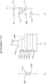
(実施例1の走査サイリスタ)
図7(a)〜(c)は、図1中の走査サイリスタ110を示す構成図である。
(Scanning Thyristor of Example 1)
7A to 7C are block diagrams showing the
図7(a)は、走査サイリスタ110の回路シンボルを示し、アノードA、カソードK、第1ゲートGP1、及び第2ゲートGP2の4つの端子を有している。
FIG. 7A shows a circuit symbol of the
図7(b)は、走査サイリスタ110の断面構造を示す図である。走査サイリスタ110は、例えば、公知のMO−CVD(Metal Organic-Chemical Vapor Deposition)法により、P型GaAsウェハ基材110aの上層に、所定の結晶をエピタキシャル成長させることで製造される。
FIG. 7B is a diagram showing a cross-sectional structure of the
即ち、P型GaAsウェハ基材110aの上層に、AlGaAs材料にP型不純物を含ませたP型層110bと、N型不純物を含ませ成層したN型層110cと、P型不純物を含ませたP型層110dと、N型不純物を含ませ成層したN型層110eと、P型不純物を含ませたP型層110fと、N型不純物を含ませ成層したN型層110gとを順に積層させたPNPNPNの6層構造のウェハを形成する。次に、公知のエッチング法を用いて溝部を形成することで、素子分離を行う。
That is, an upper layer of the P-type GaAs wafer substrate 110a includes a P-
前記エッチングの過程で、P型層110dの一部の領域を露出させ、この領域に金属配線を形成して第2ゲートGP2を形成する。同様に、前記エッチングの過程でP型層110fの一部の領域を露出させ、この領域に金属配線を形成して第1ゲートGPlを形成する。更に、最上層となるN型層110gの一部の領域を露出させ、この領域の一部に金属配線を形成してカソードKを形成する。その後、P型GaAsウェハ基材110aの底面に金属電極を形成して、アノードAを形成する。
In the etching process, a partial region of the P-
なお、図7(b)に示す構成は、P型GaAsウェハ基材110aを用いているが、これはー構成例であって、P型層110b上層の一部を露出させてこれに金属電極を形成してアノードAとすることも可能である。あるいは、P型GaAsウェハ基材110aに代えて、半絶縁性GaAs基板やシリコンウェハ基板等を用いることも可能である。
The configuration shown in FIG. 7B uses a P-type GaAs wafer substrate 110a. This is a configuration example, and a part of the upper layer of the P-
図7(c)は、図7(b)と対比させて描いた走査サイリスタ110の等価回路図である。走査サイリスタ110は、PNPトランジスタ(以下「PNPTR」という。)111,113と、NPNトランジスタ(以下「NPNTR」という。)112,114とにより構成されている。PNPTR111のエミッタが走査サイリスタ110のアノードAに相当し、NPNTR112のベースが走査サイリスタ110の第2ゲートGP2に相当し、NPNTR114のベースが走査サイリスタ110の第1ゲートGP1に相当し、NPNTR114のエミッタが走査サイリスタ110のカソードKに相当している。
FIG. 7C is an equivalent circuit diagram of the
PNPTR111のコレクタは、NPNTR112のベース及びPNPTR113のエミッタに接続され、PNPTR111のベースがNPNTR112のコレクタに接続されている。NPNTR112のエミッタは、PNPTR113のベース及びNPNTR114のコレクタに接続され、PNPTR113のコレクタがNPNTR114のベースに接続されている。
The collector of PNPTR 111 is connected to the base of
なお,図7に示した走査サイリスタ110では、GaAsウェハ基材110a上にAlGaAs層を構成したものであるが、これに限定されるものではなく、GaP、GaAsP、AlGaInP、InGaAsP等といった材料を用いるものであっても良く、あるいは、サファイヤ基板上にGaNやAlGaN、InGaN等といった材料を成膜したものであっても良い。
In the
(実施例1の発光サイリスタ)
図1中の発光サイリスタ210としては、図7に示したPNPNPNの6層からなる4端子サイリスタを用いることもできるが、図7に示したPNPNPNの6層構造のウェハを元に、図1に示したような3端子発光サイリスタとして構成することもできる。
(Light Emitting Thyristor of Example 1)
As the light-emitting
これについて説明すると、図7に示したN型層110g及びP型層110fをエッチング法により選択的に除去することで、P型GaAsウェハ基材110a、P型層110b、N型層110c、P型層110d、及びN型層110eからなるPNPNの4層を得ることができる。次いで、N型層110eの一部の領域を除去してP型層110dを露出させ、これに金属電極を形成してゲートとする。更に、N型層110eの一部の領域を除去すると共に、このN型層110eの上部に金属電極を形成してカソードとする。このようにして発光サイリスタ210を形成することができる。
This will be described. By selectively removing the N-
(実施例1のプリントヘッドの概略動作)
図1のプリントヘッド13において、クロック制御回路71から出力される制御信号C1,C2の内、制御信号C1がHレベルになると、これがインバータ72で反転され、Lレベルの第1クロックがクロック端子CK1から出力される。この第1クロックは、接続コネクタ90−2、接続ケーブル80−2、接続コネクタ90−5、及び抵抗151を介して、走査サイリスタ110−1のカソードへ供給されるので、このカソードがLレベルになる。制御信号C2がLレベルになると、これがインバータ73で反転され、Hレベルの第2クロックがクロック端子CK2から出力される。この第2クロックは、接続コネクタ90−3、接続ケーブル80−3、接続コネクタ90−6、及び抵抗152を介して走査サイリスタ110−1の第1ゲートGP1へ供給されるので、この第1ゲートGP1がHレベルになる。これにより、走査サイリスタ110−1がオン状態になって走査回路部100がシフト動作を開始し、次段以降の走査サイリスタ110−2〜110−nの第1ゲートGP1が順にHレベルになって順次オンして行く。
(Schematic operation of the print head of Example 1)
In the
発光サイリスタ210−1〜210−nの動作を考えるにあたり、走査サイリスタ110−1〜110−nのオンしている走査サイリスタ(例えば、110−2)に着目すると、その第1ゲートGPlが電源電圧VDD(例えば、3.3V)に略等しいHレベルになっている。発光サイリスタ210−2のアノードはVDD電源に接続されており、そのカソードがLレベルにされると、発光サイリスタ210−2のアノード・カソード間には電圧が印加される。 In considering the operation of the light emitting thyristors 210-1 to 210-n, when focusing on the scanning thyristors (for example, 110-2) in which the scanning thyristors 110-1 to 110-n are turned on, the first gate GP1 is connected to the power supply voltage. The H level is substantially equal to VDD (for example, 3.3 V). The anode of the light emitting thyristor 210-2 is connected to the VDD power supply. When the cathode of the light emitting thyristor 210-2 is set to the L level, a voltage is applied between the anode and the cathode of the light emitting thyristor 210-2.
一方、走査サイリスタ110−2の第1ゲートGP1と、発光サイリスタ210−2のゲートとは、それぞれ接続されているため、走査サイリスタ110−2の第1ゲートGP1と発光サイリスタ210−2のゲートとが同電位となる。この時、発光指令されている発光サイリスタ210−2のゲートのみが選択的にHレベルにされるので、発光サイリスタ210−2のゲートからカソード間にトリガ電流を生じ、この発光サイリスタ210−2がターンオンすることになる。この際、発光サイリスタ210−2のカソードに流れる電流は、データ端子DAに流入する電流(即ち、駆動電流Iout)であって、その発光サイリスタ210−2が発光状態となって駆動電流Ioutの値に応じた光出力を生じる。 On the other hand, since the first gate GP1 of the scanning thyristor 110-2 and the gate of the light emitting thyristor 210-2 are connected to each other, the first gate GP1 of the scanning thyristor 110-2 and the gate of the light emitting thyristor 210-2 are connected. Become the same potential. At this time, since only the gate of the light-emitting thyristor 210-2 that is instructed to emit light is selectively set to the H level, a trigger current is generated between the gate of the light-emitting thyristor 210-2 and the cathode, and the light-emitting thyristor 210-2 It will turn on. At this time, the current that flows to the cathode of the light-emitting thyristor 210-2 is a current that flows into the data terminal DA (that is, the drive current Iout). The light output corresponding to
(実施例1のプリントヘッドの詳細動作)
図8は、図1のプリントヘッド13の詳細な動作を示すタイミングチャートである。
(Detailed Operation of Printhead of Example 1)
FIG. 8 is a timing chart showing the detailed operation of the
この図8では、図2の画像形成装置1での印刷動作時における1ライン走査において、図1の発光サイリスタ210−1〜210−n(例えば、n=6)を順次点灯させる場合の動作波形が示されている。
In FIG. 8, the operation waveforms when the light emitting thyristors 210-1 to 210-n (for example, n = 6) in FIG. 1 are sequentially turned on in one line scanning during the printing operation in the
本実施例1のように、走査サイリスタ110を用いた走査回路部100の場合、クロック端子CK1,CK2から供給される2相のクロックが用いられ、この2相のクロックは、クロック駆動回路70から出力される。
As in the first embodiment, in the case of the scanning circuit unit 100 using the
図8のタイミングチャートにおいて、左端部に示す時刻t1の状態においては、クロック駆動回路70内のクロック制御回路71から出力される制御信号C1,C2がLレベルになる。Lレベルの制御信号C1は、インバータ72で反転され、クロック端子CK1から出力される第1クロックがHレベルになる。このHレベルは、走査回路部100側の抵抗151を介して、奇数段の走査サイリスタ110−1,110−3,・・・,110−(n−1)のカソードへ送られる。これにより、奇数段の走査サイリスタ110−1,110−3,・・・,110−(n−1)の組のアノード・カソード間電圧は略ゼロとなり、そのカソード電流が遮断されて奇数段の走査サイリスタ110−1,110−3,・・・,110−(n−1)の組がオフ状態になる。
In the timing chart of FIG. 8, in the state at the time t1 shown at the left end, the control signals C1 and C2 output from the
この時、Lレベルの制御信号C2もインバータ73で反転され、クロック端子CK2から出力される第2クロックが、a部に示すように、Hレベルになる。このHレベルは、抵抗152を介して、偶数段の走査サイリスタ110−2,110−4,・・・,110−nのカソードへ送られる。これにより、偶数段の走査サイリスタ110−2,110−4,・・・,110−nの組のアノード・カソード間電圧は略ゼロとなり、そのカソード電流が遮断されて偶数段の走査サイリスタ110−2,110−4,・・・,110−nの組もまたオフ状態になる。 At this time, the control signal C2 at the L level is also inverted by the inverter 73, and the second clock output from the clock terminal CK2 becomes the H level as shown in part a. This H level is sent to the cathodes of the even-numbered scanning thyristors 110-2, 110-4,. Thereby, the anode-cathode voltage of the set of even-numbered scanning thyristors 110-2, 110-4,..., 110-n becomes substantially zero, the cathode current is cut off, and the even-numbered scanning thyristor 110-. The group of 2,110-4,..., 110-n is also turned off.
又、時刻t1では、データ制御回路61から出力される制御信号DRVONは、Lレベルであり、これがインバータ62で反転され、抵抗63を介してデータ端子DAがHレベルになる。そのため、共通端子INを介して発光サイリスタ210(=210−1〜210−n)のカソードがHレベルであり、アノード・カソード間電圧は略ゼロとなってそのカソード電流が遮断され、発光サイリスタ210−1〜210−nもまたオフ状態になる。以下、
At time t1, the control signal DRVON output from the
(1) 初段(1段目)走査サイリスタ110−1のターンオン過程
(2) 2段目走査サイリスタ110−2のターンオン過程
(3) ゲート電流の経路
について説明する。
(1) Turn-on process of the first stage (first stage) scanning thyristor 110-1 (2) Turn-on process of the second stage scanning thyristor 110-2 (3) The path of the gate current will be described.
(1) 初段(1段目)走査サイリスタ110−1のターンオン過程
図8の時刻t2において、制御信号C1がHレベルとなり、これがインバータ72で反転され、クロック端子CK1から出力される第1クロックが、b部に示すように、Lレベルに立ち下がる。この時、制御信号C2はLレベルであり、これがインバータ73で反転され、クロック端子CK2から出力される第2クロックがHレベルのままである。このHレベルは、抵抗152、走査サイリスタ110−1の第1ゲートGP1及びカソード間を通り、抵抗151を介してクロック端子CK1に至る経路に電流を生じ、この電流をトリガ電流として走査サイリスタ110−1がターンオンすることになる。
(1) Turn-on process of first stage (first stage) scanning thyristor 110-1 At time t2 in FIG. 8, the control signal C1 becomes H level, which is inverted by the
典型的な設計例では、発光サイリスタ110−1をオンさせようとする時、この第1ゲートGP1及びカソード間電圧が略1.6Vである。又、電源電圧VDDは3.3Vであって、前記クロック端子CK2のHレベル電圧が電源電圧VDDと略等しく、発光サイリスタ110−1にゲート電流を生じさせるのに十分な値となっている。 In a typical design example, when the light emitting thyristor 110-1 is to be turned on, the voltage between the first gate GP1 and the cathode is approximately 1.6V. The power supply voltage VDD is 3.3V, and the H level voltage of the clock terminal CK2 is substantially equal to the power supply voltage VDD, which is a value sufficient to generate a gate current in the light emitting thyristor 110-1.
そのため、発光サイリスタ110−1をターンオンさせようとするとき、このカソードには従来技術のようなアンダシュート波形を与える必要はない。それ故、図1のクロック駆動回路70には、従来技術で用いられている微分回路からなるアンダシュート発生回路を設ける必要がなく、それを構成するためにクロック端子当たり2個の出力端子を設ける必要もなく、経済性に優れた構成が実現されている。
Therefore, when the light emitting thyristor 110-1 is to be turned on, it is not necessary to give an undershoot waveform to this cathode as in the prior art. Therefore, the
前記時刻t2の直後に走査サイリスタ110−1がオンすると、この第1ゲートGP1の電位がアノード電位に略等しいものとなる。 When the scanning thyristor 110-1 is turned on immediately after the time t2, the potential of the first gate GP1 becomes substantially equal to the anode potential.
時刻t3において、データ駆動回路60内のデータ制御回路61から出力される制御信号DRVONがHレベルに立ち上がり、これがインバータ62で反転され、抵抗63を介してデータ端子DAがLレベルに遷移する。この時、走査サイリスタ110−1はオンしているので、この第1ゲートGP1に対してゲート電位を共有している発光サイリスタ210−1のゲート電位がHレベルである。これにより、発光サイリスタ210−1のアノード・カソード間には電源電圧VDDと略等しい電圧が印加される。従って、発光サイリスタ210−1のゲートにはゲート電流を生じてこの発光サイリスタ210−1がオンし、このカソードには、c部に示すように、駆動電流Ioutを生じ、この駆動電流Ioの値に応じた発光出力を生じる。
At time t3, the control signal DRVON output from the
時刻t4において、制御信号DRVONがLレベルに立ち下がり、これがインバータ62で反転され、抵抗63を介してデータ端子DAがHレベルに遷移する。これにより、共通端子INを介して、発光サイリスタ210−1のアノード・カソード間電圧は略ゼロとなってオフし、d部に示すように、駆動電流Ioutが略ゼロとなる。
At time t4, the control signal DRVON falls to the L level, which is inverted by the
本実施例1では、発光サイリスタ210−1を発光させて、図2中の感光体ドラム11上に潜像を形成することができる。この時の露光エネルギー量は、前記駆動電流Ioutの値に応じて定まる発光パワーと露光時間(=t4−t3)との積であり、発光サイリスタ210−1等に製造ばらつきに起因する発光効率の差があったとしても、前記露光時間を素子毎に調整することで、露光エネルギー量のばらつきを補正することができる。又、発光サイリスタ210−1を発光させる必要のない場合には、時刻t3から時刻t4の間の制御信号DRVONをLレベルのままとする。このように、制御信号DRVONによって発光サイリスタ210の発光の有無もまた制御することができる。
In the first exemplary embodiment, the light emitting thyristor 210-1 can emit light to form a latent image on the
(2) 2段目走査サイリスタ110−2のターンオン過程
時刻t5において、制御信号C2がHレベルに立ち上がり、これがインバータ73で反転され、e部に示すように、クロック端子CK2から出力される第2クロックがLレベルに立ち下がる。
(2) Turn-on process of second-stage scanning thyristor 110-2 At time t5, the control signal C2 rises to the H level, is inverted by the inverter 73, and is output from the clock terminal CK2 as shown in section e. The clock falls to the L level.
時刻t5の直前において、クロック端子CKlから出力される第1クロックはLレベルとなり、走査サイリスタ110−1がオン状態である。そのため、クロック端子CK2がLレベルとなることで、走査サイリスタ110−1の第2ゲートGP2から抵抗120−2、発光サイリスタ210−2の第1ゲートGP1・カソード間、及び抵抗152を経由してクロック端子CK2に至る経路に電流が流れ、発光サイリスタ210−2がターンオンする。
Immediately before time t5, the first clock output from the clock terminal CKl becomes L level, and the scanning thyristor 110-1 is in the ON state. Therefore, when the clock terminal CK2 becomes L level, the second gate GP2 of the scanning thyristor 110-1 passes through the resistor 120-2, the first gate GP1 and the cathode of the light emitting thyristor 210-2, and the
前述したように、典型的な設計例では、発光サイリスタ210−2の第1ゲートGP1及びカソード間電圧が略1.6Vである。又、電源電圧VDDは3.3Vであり、前記走査サイリスタ110−1における第2ゲートGP2のHレベル電圧は電源電圧VDDと略等しく、発光サイリスタ210−2にゲート電流を生じさせるのに十分な値となっている。そのため、発光サイリスタ210−2をターンオンさせようとする時、従来のようにそのカソードにアンダシュート波形を与える必要はない。 As described above, in a typical design example, the voltage between the first gate GP1 and the cathode of the light emitting thyristor 210-2 is approximately 1.6V. The power supply voltage VDD is 3.3 V, and the H level voltage of the second gate GP2 in the scanning thyristor 110-1 is substantially equal to the power supply voltage VDD, which is sufficient to generate a gate current in the light emitting thyristor 210-2. It is a value. Therefore, when the light emitting thyristor 210-2 is to be turned on, it is not necessary to give an undershoot waveform to the cathode as in the prior art.
時刻t6において、制御信号C1がLレベルに立ち下がり、これがインバータ72で反転され、f部に示すように、クロック端子CK1から出力される第1パルスがHレベルに立ち上がる。これにより、抵抗151を介して走査サイリスタ110−1のカソード電位が上昇し、アノード・カソード間電圧が急激に減少して、この走査サイリスタ110−1はターンオフする。
At time t6, the control signal C1 falls to the L level, which is inverted by the
時刻t7において、制御信号DRVONがHレベルに立ち上がり、これがインバータ62で反転され、抵抗63を介してデータ端子DAがLレベルに遷移する。データ端子DAがLレベルに遷移すると、共通端子INを介して発光サイリスタ210−2のアノード・カソード間には、電源電圧VDDと略等しい電圧が印加される。
At time t7, the control signal DRVON rises to H level, which is inverted by the
前述したように、時刻t5においては走査サイリスタ110−2がオン状態にあり、走査サイリスタ110−1がオフ状態になっている。このように、走査サイリスタ110−2はオンしているので、この走査サイリスタ110−2の第1ゲートGP1に対してゲート電位を共有している発光サイリスタ210−2がオンし、このカソードには、g部に示すように、駆動電流Ioutを生じてこの駆動電流Ioutの値に応じた発光出力を生じる。 As described above, at time t5, scanning thyristor 110-2 is in the on state, and scanning thyristor 110-1 is in the off state. As described above, since the scanning thyristor 110-2 is turned on, the light emitting thyristor 210-2 sharing the gate potential with the first gate GP1 of the scanning thyristor 110-2 is turned on, , G, a drive current Iout is generated, and a light emission output corresponding to the value of the drive current Iout is generated.
時刻t8において、制御信号DRVONがLレベルに立ち下がり、これがインバータ62で反転され、抵抗63を介してデータ端子DAがHレベルに遷移する。これにより、発光サイリスタ210−2のアノード・カソード間電圧が略ゼロとなってこの発光サイリスタ210−2はオフし、h部に示すように、駆動電流Ioutが略ゼロとなる。
At time t8, the control signal DRVON falls to the L level, which is inverted by the
時刻t9において、制御信号C1がHレベルになり、これがインバータ72で反転され、クロック端子CK1から出力される第1クロックが、i部に示すように、Lレベルに立ち下がる。これにより、走査サイリスタ110−3はターンオンする。
At time t9, the control signal C1 becomes H level, this is inverted by the
以下同様に、第1、第2クロック端子CK1,CK2から出力される第1、第2クロックの遷移と制御信号DRVONのオン、オフとが順に発生して、発光サイリスタ210−3〜210−nを順次点灯することができる。 Similarly, the transitions of the first and second clocks output from the first and second clock terminals CK1 and CK2 and the turning on and off of the control signal DRVON occur in order, and the light emitting thyristors 210-3 to 210-n. Can be turned on sequentially.
(3) ゲート電流の経路
図9は、図1中の走査回路部100における走査サイリスタ110−1〜110−3の詳細動作を説明するための要部の回路図である。
(3) Path of Gate Current FIG. 9 is a circuit diagram of a main part for explaining detailed operations of the scanning thyristors 110-1 to 110-3 in the scanning circuit unit 100 in FIG.
図9において、Vce1はPNPTR111−2のコレクタ・エミッタ間電圧、Vce2はPNPTR113−2のコレクタ・エミッタ間電圧、及び、VbeはNPNTR114−3のベース・エミッタ間電圧である。 In FIG. 9, Vce1 is the collector-emitter voltage of PNPTR 111-2, Vce2 is the collector-emitter voltage of PNPTR 113-2, and Vbe is the base-emitter voltage of NPNTR 114-3.
初段の走査サイリスタ110−1は、図7(c)と同様に、2つのPNPTR111−1,113−1及び2つのNPNTR112−1,114−1により構成されている。同様に、2段目の走査サイリスタ110−2は、2つのPNPTR111−2,113−2及び2つのNPNTR112−2,114−2により構成され、3段目の走査サイリスタ110−3は、2つのPNPTR111−3,113−3及び2つのNPNTR112−3,114−3により構成されている。 The first-stage scanning thyristor 110-1 is composed of two PNPTRs 111-1 and 113-1 and two NPNTRs 112-1 and 114-1, as in FIG. 7C. Similarly, the second-stage scanning thyristor 110-2 includes two PNPTRs 111-2 and 113-2 and two NPNTRs 112-2 and 114-2, and the third-stage scanning thyristor 110-3 includes two PNPTRs 111-3 and 113-3 and two NPNTRs 112-3 and 114-3 are included.
なお、図9の回路図では、図示を簡略化する目的で、走査サイリスタ110−1〜110−3における第2ゲートGP2とVDD電源との間の図1中の抵抗140−1〜140−3の図示を省略している。更に、走査サイリスタ110−2,110−3における第1ゲートGP1とグランドGNDとの間の抵抗130−2,130−3の図示を省略している。 In the circuit diagram of FIG. 9, for the purpose of simplifying the illustration, the resistors 140-1 to 140-3 in FIG. 1 between the second gate GP2 and the VDD power supply in the scanning thyristors 110-1 to 110-3. Is omitted. Further, the resistors 130-2 and 130-3 between the first gate GP1 and the ground GND in the scanning thyristors 110-2 and 110-3 are not shown.
前述したように、走査サイリスタ110−1のターンオン過程において、第1ゲートGP1は電源電圧VDDと略等しいHレベルとなり、クロック端子CK1をLレベルにすることで、走査サイリスタ110−1にゲート電流を生じさせてこの走査サイリスタ110−1をターンオンする。 As described above, in the turn-on process of the scanning thyristor 110-1, the first gate GP1 becomes H level substantially equal to the power supply voltage VDD, and the gate terminal is supplied with the gate current to the scanning thyristor 110-1 by setting the clock terminal CK1 to L level. As a result, the scanning thyristor 110-1 is turned on.
次いで、走査サイリスタ110−2のターンオン過程に移るのであるが、説明を簡略化するために、走査サイリスタ110−3のターンオン過程について取り上げる。この時、走査サイリスタ110−2はオンしており、目標とすべき走査サイリスタ110−3のターンオン過程において、誤ってその前段である走査サイリスタ110−1が再びオンしないことを説明する。これにより、一般性を失うことなく、前段から後段の走査サイリスタ110にオン状態が引き継がれることを説明することができる。
Next, the process proceeds to the turn-on process of the scanning thyristor 110-2. In order to simplify the description, the turn-on process of the scanning thyristor 110-3 will be taken up. At this time, the scanning thyristor 110-2 is turned on, and it will be explained that the scanning thyristor 110-1 as the preceding stage is not erroneously turned on again in the turn-on process of the scanning thyristor 110-3 to be targeted. Thus, it can be explained that the ON state is inherited from the preceding stage to the
走査サイリスタ110−2が単独でオンとなる状態は、クロック端子CK1がLレベルで、且つクロック端子CK2がHレベルとなる間(即ち、図8における時刻t6〜t9間)に相当するものである。次いで、走査サイリスタ110−3をターンオンするために、図8のi部に示すように、クロック端子CK1をLレベルに立ち下げる。 The state in which the scanning thyristor 110-2 is turned on independently corresponds to the period when the clock terminal CK1 is at the L level and the clock terminal CK2 is at the H level (that is, between time t6 and time t9 in FIG. 8). . Next, in order to turn on the scanning thyristor 110-3, the clock terminal CK1 is lowered to the L level as shown in part i of FIG.
この時、走査サイリスタ110−2はオンしているので、PNPTR111−2もまたオンしており、このエミッタ・コレクタ間電圧Vce1が小さく、理想的には略0Vとなっている。そのため、走査サイリスタ110−2における第2ゲートGP2の電位は、電源電圧VDDに略等しい。 At this time, since the scanning thyristor 110-2 is on, the PNPTR 111-2 is also on, and the emitter-collector voltage Vce1 is small, ideally approximately 0V. Therefore, the potential of the second gate GP2 in the scanning thyristor 110-2 is substantially equal to the power supply voltage VDD.
その結果、図9の破線矢印で示すように、VDD電源に接続されている走査サイリスタ110−2のアノードAから第2ゲートGP2、抵抗120−3、走査サイリスタ110−3の第1ゲートGP1、及びNPNTR114−3のベース・エミッタ間を通り、抵抗151を経由してクロック端子CK1に至る経路に電流I1が流れる。
As a result, as indicated by a broken line arrow in FIG. 9, the second gate GP2, the resistor 120-3, and the first gate GP1 of the scan thyristor 110-3 from the anode A of the scan thyristor 110-2 connected to the VDD power source, And the current I1 flows through the path between the base and the emitter of the NPNTR 114-3 and through the
NPNTR114−3のベース・エミッタ間に電流I1が流れることで、このNPNTR114−3がオンすることになり、PNPTR113−3のベース電位を降下させる。走査サイリスタ110−3の第2ゲートGP2とVDD電源との間は、抵抗140−3により接続されており、その第2ゲートGP2がHレベルになっている。そのため、PNPTR113−3のベース電位が降下することで、このベース・エミッタ間には電圧を生じ、PNPTR113−3がオンすることになる。NPNTR112−3のベース・エミッタ間においても同様であり、NPNTR112−3もまたオンする。NPNTR112−3がオンすると、このNPNTR112−3のコレクタ電位、即ちPNPTR111−3のベース電位が降下してこのPNPTR111−3のベース・エミッタ間に電圧を生じ、PNPTR111−3もまたオンする。このような過程を経て、走査サイリスタ110−3がターンオンする。 When the current I1 flows between the base and emitter of the NPNTR 114-3, the NPNTR 114-3 is turned on, and the base potential of the PNPTR 113-3 is lowered. The second gate GP2 of the scanning thyristor 110-3 and the VDD power supply are connected by a resistor 140-3, and the second gate GP2 is at the H level. Therefore, when the base potential of the PNPTR 113-3 drops, a voltage is generated between the base and the emitter, and the PNPTR 113-3 is turned on. The same applies between the base and emitter of the NPNTR 112-3, and the NPNTR 112-3 is also turned on. When the NPNTR 112-3 is turned on, the collector potential of the NPNTR 112-3, that is, the base potential of the PNPTR 111-3 drops to generate a voltage between the base and emitter of the PNPTR 111-3, and the PNPTR 111-3 is also turned on. Through such a process, the scanning thyristor 110-3 is turned on.
この時の走査サイリスタ110−1における挙動を考察してみる。
前述した走査サイリスタ110−3のターンオン過程の始まる前において、走査サイリスタ110−1はオフしている。走査サイリスタ110−3をターンオンさせるために、クロック端子CK1がLレベルになる。この時、走査サイリスタ110−1と走査サイリスタ110−2との間は、抵抗120−2を介して接続され、抵抗120−2の一端が走査サイリスタ110−1の第2ゲートGP2に接続され、抵抗120−2の他端が走査サイリスタ110−2の第1ゲートGP1に接続されている。
Consider the behavior of the scanning thyristor 110-1 at this time.
Prior to the start of the turn-on process of scan thyristor 110-3, scan thyristor 110-1 is off. In order to turn on the scanning thyristor 110-3, the clock terminal CK1 becomes L level. At this time, the scanning thyristor 110-1 and the scanning thyristor 110-2 are connected via a resistor 120-2, and one end of the resistor 120-2 is connected to the second gate GP2 of the scanning thyristor 110-1. The other end of the resistor 120-2 is connected to the first gate GP1 of the scanning thyristor 110-2.
前述したように、走査サイリスタ110−2のオン状態においては、PNPTR111−2がオン状態であり、このコレクタ・エミッタ間電圧Vce1は小さく、走査サイリスタ110−2の第2ゲートGP2がHレベルとなっている。又、PNPTR113−2はオン状態であり、このコレクタ・エミッタ間電圧Vce2もまた小さい状態にある。この結果、走査サイリスタ110−2の第1ゲートGP1はHレベルになっている。この時、抵抗120−2を経由して走査サイリスタ110−2から走査サイリスタ110−1に流れるはずの電流I2の経路として、図9に一点鎖線で示す電流経路が考えられる。 As described above, when the scanning thyristor 110-2 is in the on state, the PNPTR 111-2 is in the on state, the collector-emitter voltage Vce1 is small, and the second gate GP2 of the scanning thyristor 110-2 is at the H level. ing. The PNPTR 113-2 is in an on state, and the collector-emitter voltage Vce2 is also in a small state. As a result, the first gate GP1 of the scanning thyristor 110-2 is at the H level. At this time, as a path of the current I2 that should flow from the scanning thyristor 110-2 to the scanning thyristor 110-1 via the resistor 120-2, a current path indicated by a one-dot chain line in FIG. 9 can be considered.
前記電流I2の経路は、VDD電源からPNPTR111−2のエミッタ・コレクタ間、PNPTR113−2のエミッタ・コレクタ間、走査サイリスタ110−2の第1ゲートGP1、抵抗120−2、走査サイリスタ110−1の第2ゲートGP2、PNPTR113−1のエミッタ・ベース間、NPNTR114−1のコレクタ・エミッタ間、及び、抵抗151を経由してクロック端子CK1に至る経路である。ところが、走査サイリスタ110−1はオフ状態にあるので、NPNTR114−1もまたオフ状態になっていて、このNPNTR114−1のコレクタ・エミッタ間には電流が流れず、前述した一点鎖線の電流I2は生じないことが判る。
The path of the current I2 is from the VDD power source to the emitter and collector of the PNPTR 111-2, between the emitter and collector of the PNPTR 113-2, the first gate GP1 of the scanning thyristor 110-2, the resistor 120-2, and the scanning thyristor 110-1. This is a path from the second gate GP2, between the emitter and base of PNPTR 113-1, between the collector and emitter of NPNTR 114-1, and via the
このように、走査サイリスタ110−2のオン状態において、クロック端子CK1をLレベルに遷移させた時、この後段の走査サイリスタ110−3はターンオンするが、前段の走査サイリスタ110−1はオンしない。 As described above, when the clock terminal CK1 is shifted to the L level in the ON state of the scanning thyristor 110-2, the subsequent scanning thyristor 110-3 is turned on, but the preceding scanning thyristor 110-1 is not turned ON.
従来の走査回路部においては、走査方向を定める目的で各走査サイリスタのゲート間をダイオードを用いて接続している。そのため、着目している走査サイリスタの後段回路にはゲートトリガ電流が伝達されるものの、前段の走査サイリスタにはゲートトリガ電流が伝達されないことになり、前述した走査方向を定めることができる。しかし、その半面、前記ダイオードの順電圧分だけ動作電源電圧が増加してしまい、そのままでは3.3Vといった標準的な回路電圧の基で動作しえない特性になっている。 In the conventional scanning circuit unit, the gates of the scanning thyristors are connected using diodes for the purpose of determining the scanning direction. Therefore, although the gate trigger current is transmitted to the subsequent circuit of the scanning thyristor of interest, the gate trigger current is not transmitted to the preceding scanning thyristor, and the above-described scanning direction can be determined. However, on the other hand, the operating power supply voltage increases by the forward voltage of the diode, and as such, it has a characteristic that cannot operate based on a standard circuit voltage of 3.3V.
このような不具合を解消する目的で、従来技術では、走査サイリスタのカソードにアンダシュート電圧を発生させることで、前記電源電庄の不足を補うようにしていたのであるが、そのためには多数の回路要素を追加しなければならず、プリントヘッドがコストアップしてしまうという別の課題を招来してしまっていたのである。 In order to solve such problems, in the prior art, the undershoot voltage is generated at the cathode of the scanning thyristor to compensate for the shortage of the power supply voltage. Elements had to be added, leading to another issue of increased printhead costs.
そこで、本実施例1では、着目している走査サイリスタ110と後段の走査サイリスタ110との間を抵抗120により接続することにより、前述したダイオードの順電圧分だけ電源電圧が不足するという不具合を解消している。更に、着目の走査サイリスタ110の第2ゲートGP2と後段の走査サイリスタ110の第1ゲートGP1とを接続した構成にしているので、着目の走査サイリスタ110の後段側にはゲートトリガ電流を流すことができる一方で、着目の走査サイリスタ110から前段の走査サイリスタ110の側にはゲートトリガ電流を生じることは無く、走査方向を一方向に定めることができる。
Therefore, in the first embodiment, by connecting the
(実施例1の効果)
本実施例1によれば、次の(a)〜(c)のような効果がある。
(Effect of Example 1)
According to the first embodiment, there are the following effects (a) to (c).
(a) 従来構成の走査回路部の駆動においては、例えば、図1のクロック駆動回路70の出力側にCR微分回路をそれぞれ設けてアンダシュート波形を生成し、2個のクロック端子CK1,CK2から2相のクロックを出力している。この際、CR微分回路においては、直流成分を伝達することができないので、2個のクロック端子CK1,CK2に対して各2個の出力端子(=合計4個の出力端子)、即ち、転送クロック当たり2個で合計4個の出力端子が必要であった。
(A) In driving the scanning circuit unit of the conventional configuration, for example, a CR differentiating circuit is provided on the output side of the
これに対し、本実施例1によれば、図1のような回路構成にすることにより、クロック駆動回路70におけるクロック端子数が転送クロック当たり1個で良く、従来構成と比べて所要端子の数を半減することができる。更に、従来構成のクロック駆動回路に備えていたキャパシタ等の外付け部品が不要になる。これにより、プリントヘッド13におけるデータ転送速度を向上できることは勿論のこと、クロック駆動回路70のクロック端子数の減少によって、回路規模の削減と、これによる低コスト化も期待できる。
On the other hand, according to the first embodiment, by adopting the circuit configuration as shown in FIG. 1, the number of clock terminals in the
(b) 初段の走査サイリスタ110−1の第1ゲートGP1は、第2クロック端子CK2に接続されているので、走査回路部100用のスタート信号が不要になる。更に、前段の走査サイリスタ110における第2ゲートGP2は、電気的接続手段としての抵抗120を介して後段の走査サイリスタ110における第1ゲートGP1にそれぞれ接続されているので、2相の第1及び第2クロックの基でも走査回路部100の走査方向を定めることができ、走査回路部100の誤動作を防止できる。しかも、電源電圧VDDとして一般的な例えば3.3Vの電源によりプリントヘッド駆動を行うことができ、省電力化が可能になる。
(B) Since the first gate GP1 of the first-stage scanning thyristor 110-1 is connected to the second clock terminal CK2, a start signal for the scanning circuit unit 100 becomes unnecessary. Furthermore, since the second gate GP2 in the preceding
(c) 本実施例1の画像形成装置1によれば、プリントヘッド13を採用しているので、スペース効率及び光取り出し効率に優れた高品質の画像形成装置1を提供することができる。即ち、プリントヘッド13を用いることにより、本実施例1のフルカラーの画像形成装置1に限らず、モノクロ、マルチカラーの画像形成装置においても効果が得られるが、特に、露光装置としてのプリントヘッド13を数多く必要とするフルカラーの画像形成装置1において一層大きな効果が得られる。
(C) According to the
本発明の実施例2における画像形成装置1では、実施例1のプリントヘッド13における回路構成の極性(即ち、P、Nの接続)を逆にした変形例を示すプリントヘッド13Aを採用している。以下、実施例1と異なる部分について説明する。
The
(実施例2のプリントヘッド)
図10は、本発明の実施例2におけるプリントヘッド13Aの構成を示す回路図であり、実施例1を示す図1中の要素と共通の要素には共通の符号が付されている。
(Print head of Example 2)
FIG. 10 is a circuit diagram showing the configuration of the print head 13A according to the second embodiment of the present invention. Elements common to those in FIG. 1 showing the first embodiment are denoted by common reference numerals.
本実施例2のプリントヘッド13Aは、実施例1の走査回路部100及び発光サイリスタアレイ200とは異なる極性の走査回路部100A及び発光サイリスタアレイ200Aを有し、これらが実施例1と同様の複数の接続ケーブル80(=80−1〜80−3)及び複数の接続コネクタ90(=90−1〜90−6)を介して、実施例1の印刷制御部40とは異なる構成の印刷制御部40Aに接続されている。走査回路部100A及び発光サイリスタアレイ200Aは、実施例1と同様に、VDD電源(例えば、3.3V)により動作する構成になっている。
The print head 13A according to the second embodiment includes a scanning circuit section 100A and a light emitting
印刷制御部40Aは、実施例1のデータ駆動回路60とは異なる構成の第1駆動回路(例えば、データ駆動回路)60Aと、実施例1と同様の第2駆動回路(例えば、クロック駆動回路)70とを有している。データ駆動回路60Aは、VDD電源により動作して発光サイリスタアレイ200A側の共通端子INをH/Lレベルに駆動する回路である。クロック駆動回路70は、実施例1と同様に、VDD電源により動作して走査回路部100Aを駆動するための2相の第1及び第2クロックを出力する回路である。
The print control unit 40A includes a first drive circuit (for example, a data drive circuit) 60A having a configuration different from that of the data drive
本実施例2において、発光サイリスタアレイ200Aを駆動する駆動装置は、実施例1と同様に、走査回路部100A、データ駆動回路60A、及びクロック駆動回路70を有している。図10では、データ駆動回路60A及びクロック駆動回路70が印刷制御部40A内に配置された構成例が示されているが、実施例1の図6と同様に、データ駆動回路60A及びクロック駆動回路70をプリントヘッド13A内に配置しても良い。
In the second embodiment, the driving device for driving the light emitting
走査回路部100Aにより走査される発光サイリスタアレイ200Aは、実施例1とは異なる極性の3端子発光素子としての例えば複数段のNゲート型発光サイリスタ210A(=210A−1〜210A−n,・・・)を有し、これらの各発光サイリスタ210Aの第1端子(例えば、アノード)が駆動電流Ioutを流す共通端子INを介して接続コネクタ90−4に接続され、第2端子(例えば、カソード)がグランドGNDに接続され、第1制御端子(例えば、ゲート)が走査回路部100Aの各出力端子Q1〜Qnに接続されている。発光サイリスタ210A−1〜210A−n,・・・の総数は、実施離1と同様に、例えば、A4サイズの用紙に1インチ当たり600ドットの解像度で印刷可能なプリントヘッド13Aの場合、4992個であり、これらが配列されることになる。
The light emitting
走査回路部100Aは、クロック駆動回路70から第1、第2クロック端子CK1,CK2、接続コネクタ90−2,90−3、接続ケーブル80−2,80−3、及び接続コネクタ90−5,90−6を介して供給される2相の第1及び第2クロックにより駆動され、発光サイリスタアレイ200Aにトリガ電流を流してオン/オフ動作させる回路である。この走査回路部100Aは、実施例1とは異なる極性の複数段の4端子スイッチ素子(例えば、PNPNPNの6層からなり、N型層に接続されたNゲートの2つの制御端子を有する4端子走査サイリスタ)110A(=110A−1〜110A−n、例えばn=4992)と、走査方向決定用の複数の電気的接続手段(例えば、実施例1と同様の抵抗)120(=120−2〜120−n)と、実施例1と同様の複数の抵抗130(=130−2〜130−n)と、実施例1と同様の複数の抵抗140(=140−1〜140−n)とを有し、自己走査型シフトレジスタにより構成されている。
The scanning circuit unit 100A includes first and second clock terminals CK1 and CK2, connection connectors 90-2 and 90-3, connection cables 80-2 and 80-3, and connection connectors 90-5 and 90 from the
各段の走査サイリスタ110A(=110A−1〜110A−n)は、第3端子(例えば、アノード)、第4端子(例えば、カソード)、第2制御端子(例えば、第1ゲート)GN1、及び第3制御端子(例えば、第2ゲート)GN2を有し、カソードが、グランドGNDに接続され、第1ゲートGN1が、各出力端子Q1〜Qnを介して各段の発光サイリスタ210Aのゲートに接続されると共に、各抵抗130(=130−2〜130−n)を介してVDD電源に接続され、第2ゲートGN2が、各抵抗140(=140−1〜140−n)を介してグランドGNDに接続されている。但し、初段の走査サイリスタ110−1の第1ゲートGN1とVDD電源との間には、実施例1と同様に抵抗130が設けられていない。
The
奇数段の走査サイリスタ110A−1,110A−3,・・・,110A−(n−1)のアノードは、抵抗151を介して接続コネクタ90−5に接続されている。偶数段の走査サイリスタ110A−2,110A−4,・・・,110A−nのアノードは、抵抗152を介して接続コネクタ90−6に接続されている。
The anodes of the odd-numbered
初段の走査サイリスタ110A−1の第1ゲートGN1は、抵抗152を介して接続コネクタ90−6に接続されている。初段から最終段までの走査サイリスタ110A−1〜110A−nにおいて、前段の走査サイリスタ110Aの第2ゲートGN2と、後段の走査サイリスタ110Aの第1ゲートGN1との間は、実施例1と同様に、各抵抗120(=120−2〜120−n)を介してそれぞれ接続されている。各抵抗120は、実施例1と同様に、走査サイリスタ110A−1〜110A−nが順次点灯する時の走査方向(例えば、図10において右方向)を決定するために設けられている。
The first gate GN1 of the first-
各段の走査サイリスタ110Aと各段の発光サイリスタ210Aとは、半導体素子として同様なレイヤ構造を有し、且つ同様な回路動作を行うものであるが、各段の発光サイリスタ210Aは、主として発光機能を用いるものであるのに対して、各段の走査サイリスタ110Aにおいては、発光機能を必要とされないので、その上層をメタル膜等の非透光性材料で覆うことで遮光して用いられる。
The
走査回路部100Aでは、実施例1と同様に、クロック駆動回路70の第1及び第2クロック端子CK1,CK2から供給される2相の第1及び第2クロックに基づき、走査サイリスタ110A−1〜110A−nが択一的にオン状態となり、このオン状態が発光サイリスタアレイ200Aに伝達され、発光サイリスタ210A−1〜210A−nの内から発光すべき発光サイリスタ210A−1〜210A−nを指令する働きをする。この走査回路部100Aにおいて、オン状態となる各段の走査サイリスタ110Aのオン状態が、2相の第1及び第2クロック毎に隣接の走査サイリスタ110Aに伝達され、シフトレジスタと同様の回路動作が行われる構成になっている。
In the scanning circuit unit 100A, as in the first embodiment, the
なお、2段目〜最終段の走査サイリスタ110A−2〜110A−nにおける各第1ゲートGN1は、各抵抗130−2〜130−nを介してそれぞれVDD電源に接続されているが、初段の走査サイリスタ110A−1における第1ゲートGN1とVDD電源との間の抵抗130は削除されている。これは実施例1と同様に、部品点数を削減するための工夫であって、低コスト化への配慮が不要である場合には、初段の走査サイリスタ110A−1における第1ゲートGN1とVDD電源との間に抵抗130を設ける構成とすることもできる。
The first gates GN1 in the second to
又、実施例1と同様に、各段の抵抗130(=130−2〜130−n)や抵抗140(=140−1〜140−n)は、走査回路部100Aの動作を確実にする目的で設けるものであるが、走査サイリスタ110A(=110A−1〜110A−n)の特性によっては、そのいずれか一方、もしくは全部を省略することもできる。
Similarly to the first embodiment, the resistors 130 (= 130-2 to 130-n) and the resistors 140 (= 140-1 to 140-n) at each stage are intended to ensure the operation of the scanning circuit unit 100A. However, depending on the characteristics of the
前記発光サイリスタアレイ200Aに接続された複数のデータ駆動回路60Aは、実施例1とは異なる負論理の駆動指令信号である第1制御信号DRVON−Nを生成し、複数の発光サイリスタアレイ200Aを時分割駆動するためのデータとしての駆動電流Ioutを共通端子INに流す回路である。図10においては、実施例1の図1と同様に、説明を簡略化するために1個のデータ駆動回路60Aのみが図示されている。
The plurality of data driving circuits 60A connected to the light emitting
データ駆動回路60Aは、実施例1とは異なる制御信号DRVON−Nを生成するデータ制御回路61Aと、制御信号DRVON−Nを反転する実施例1と同様のインバータ62と、実施例1と同様に、インバータ62とデータ端子DAとの間に接続された抵抗63とを有している。
The data driving circuit 60A includes a
例えば、データ制御回路61Aから出力される制御信号DRVON−NがHレベルの場合、PMOS66aがオフ状態、NMOS66bがオン状態になり、抵抗63、データ端子DA及び共通端子INを介して発光サイリスタ210AのアノードがLレベルになる。そのため、発光サイリスタ210Aのアノード・カソード間電圧が略ゼロとなって、共通端子INに流れる駆動電流Ioutがゼロとなり、発光サイリスタ210A−1〜210A−nを全て非発光状態にできる。
For example, when the control signal DRVON-N output from the
これに対し、制御信号DRVON−NがLレベルの場合、PMOS66aがオン状態、NMOS66bがオフ状態になり、抵抗63、データ端子DA及び共通端子INを介して発光サイリスタ210AのアノードがHレベルになる。これにより、発光サイリスタ210A−1〜210A−nのアノード・カソード間には、電源電圧VDDと略等しい電圧が印加されることになる。この時、発光サイリスタ210A−1〜210A−n内の1つの発光サイリスタ210Aに対して点灯指令がされると、VDD電源からPMOS62a、抵抗63、データ端子DA、共通端子IN、及び発光サイリスタ210Aのアノード・カソード端子間を経由してグランドGNDに至る経路に駆動電流Ioutが流れ、その発光サイリスタ210Aが点灯する。
On the other hand, when the control signal DRVON-N is at the L level, the PMOS 66a is turned on, the NMOS 66b is turned off, and the anode of the
(実施例2の走査サイリスタ)
図11(a)〜(c)は、図10中の走査サイリスタ110Aを示す構成図である。
(Scanning thyristor of Example 2)
FIGS. 11A to 11C are configuration diagrams showing the
図11(a)は、走査サイリスタ110Aの回路シンボルを示し、アノードA、カソードK、第1ゲートGN1、及び第2ゲートGN2の4つの端子を有している。
FIG. 11A shows a circuit symbol of the
図11(b)は、走査サイリスタ110Aの断面構造を示す図である。走査サイリスタ110Aは、例えば、公知のMO−CVD法により、N型GaAsウェハ基材115aの上層に、所定の結晶をエピタキシャル成長させることで製造される。
FIG. 11B is a diagram showing a cross-sectional structure of the
即ち、N型GaAsウェハ基材115aの上層に、AlGaAs材料にN型不純物を含ませたN型層115bと、P型不純物を含ませ成層したP型層115cと、N型不純物を含ませたN型層115dと、P型不純物を含ませ成層したP型層115eと、N型不純物を含ませたN型層115fと、P型不純物を含ませ成層したP型層115gとを順に積層させたPNPNPNの6層構造のウェハを形成する。次に、公知のエッチング法を用いて溝部を形成することで、素子分離を行う。
That is, an N-
前記エッチングの過程で、N型層115dの一部の領域を露出させ、この領域に金属配線を形成して第2ゲートGN2を形成する。同様に、前記エッチングの過程でN型層115fの一部の領域を露出させ、この領域に金属配線を形成して第1ゲートGNlを形成する。更に、最上層となるP型層115gの一部の領域を露出させ、この領域の一部に金属配線を形成してアノードAを形成する。その後、N型GaAsウェハ基材115aの底面に金属電極を形成して、カソードKを形成する。
In the etching process, a part of the N-
なお、図11(b)に示す構成は、N型GaAsウェハ基材115aを用いているが、これはー構成例であって、N型層115b上層の一部を露出させてこれに金属電極を形成してカソードKとすることも可能である。あるいは、N型GaAsウェハ基材115aに代えて、半絶縁性GaAs基板やシリコンウェハ基板等を用いることも可能である。
The configuration shown in FIG. 11B uses an N-type
図11(c)は、図11(b)と対比させて描いた走査サイリスタ110Aの等価回路図である。走査サイリスタ110Aは、2つのNPNTR116,118と、2つのPNPTR117,119とにより構成されている。PNPTR119のエミッタが走査サイリスタ110AのアノードAに相当し、PNPTR119のベースが走査サイリスタ110Aの第1ゲートGN1に相当し、PNPTR117のベースが走査サイリスタ110Aの第2ゲートGN2に相当し、NPNTR116のエミッタが走査サイリスタ110AのカソードKに相当している。
FIG. 11C is an equivalent circuit diagram of the
又、PNPTR119のコレクタが、NPNTR118のベースとNPNTR117のエミッタに接続され、PNPTR119のベースが、NPNTR118のコレクタに接続され、PNPTR117のベースが、NPNTR118のエミッタとNPNTR116のコレクタに接続され、PNPTR117のコレクタが、NPNTR116のベースに接続されている。
Also, the collector of
なお、図11に示した走査サイリスタ110Aでは、GaAsウェハ基材115a上にAlGaAs層を構成したものであるが、これに限定されるものではなく、GaP、GaAsP、AlGaInP、InGaAsP等といった材料を用いるものであっても良く、あるいは、サファイヤ基板上にGaNやAlGaN、InGaN等といった材料を成膜したものであっても良い。
In the
(実施例2の発光サイリスタ)
図10中の発光サイリスタ210Aとしては、図11に示したPNPNPNの6層からなる4端子サイリスタを用いることもできるが、図11に示したPNPNPNの6層構造のウェハを元に、図10に示したような3端子サイリスタとして構成することもできる。
(Light-emitting thyristor of Example 2)
As the light-emitting
これについて説明すると、図11に示したP型層115g及びN型層115fをエッチング法により選択的に除去することで、N型層115b、P型層115c、N型層115d、及びP型層115eからなるPNPNの4層を得ることができる。次いで、P型層115eの一部の領域を除去してN型層115dを露出させ、これに金属電極を形成してゲートとする。更に、P型層115eの一部の領域を除去すると共に、このP型層115eの上部に金属電極を形成してアノードとする。このようにして発光サイリスタ210Aを形成することができる。
This will be described below. By selectively removing the P-
(実施例2のプリントヘッドの概略動作)
図10のプリントヘッド13Aにおいて、クロック制御回路71から出力される制御信号C1,C2の内、制御信号C1がLレベルになると、これがインバータ72で反転され、Hレベルの第1クロックがクロック端子CK1から出力される。この第1クロックは、接続コネクタ90−2、接続ケーブル80−2、接続コネクタ90−5、及び抵抗151を介して、走査サイリスタ110A−1のアノードへ供給されるので、このアノードがHレベルになる。制御信号C2がLレベルになると、これがインバータ73で反転され、Hレベルの第2クロックがクロック端子CK2から出力される。この第2クロックは、接続コネクタ90−3、接続ケーブル80−3、接続コネクタ90−6、及び抵抗152を介して走査サイリスタ110A−1の第1ゲートGN1へ供給されるので、この第1ゲートGN1がHレベルになる。これにより、走査サイリスタ110A−1がオン状態になって走査回路部100Aがシフト動作を開始し、次段以降の走査サイリスタ110A−2〜110A−nの第1ゲートGN1が順にHレベルになって順次オンして行く。
(Schematic operation of the print head of Example 2)
In the print head 13A of FIG. 10, when the control signal C1 of the control signals C1 and C2 output from the
発光サイリスタ210A−1〜210A−nの動作を考えるにあたり、走査サイリスタ110A−1〜110A−nのオンしている走査サイリスタ(例えば、110A−2)に着目すると、その第1ゲートGNlがグランド電位に略等しいLレベルになっている。一方、走査サイリスタ110A−2の第1ゲートGN1と、発光サイリスタ210A−2のゲートとは、それぞれ接続されているため、走査サイリスタ110A−2の第1ゲートGN1と発光サイリスタ210A−2のゲートとが同電位となる。
In considering the operation of the
発光サイリスタ210A−2のカソードは、グランドGNDに接続されており、そのアノードがHレベルにされると、この発光サイリスタ210A−2のアノード・カソード間に電圧が印加される。この時、発光指令されている発光サイリスタ210A−2のゲートのみが選択的にLレベルにされるので、この発光サイリスタ210A−2のアノードからゲート間にトリガ電流を生じ、この発光サイリスタ210A−2がターンオンすることになる。この際、発光サイリスタ210A−2のカソードに流れる電流は、データ端子DAから流出する電流(即ち、駆動電流Iout)であって、その発光サイリスタ210A−2が発光状態となって駆動電流Ioutの値に応じた光出力を生じる。
The cathode of the
(実施例2のプリントヘッドの詳細動作)
図12は、図10のプリントヘッド13Aの詳細な動作を示すタイミングチャートである。
(Detailed Operation of Printhead of Example 2)
FIG. 12 is a timing chart showing the detailed operation of the print head 13A shown in FIG.
この図12では、実施例1と同様に、図2の画像形成装置1での印刷動作時における1ライン走査において、図10の発光サイリスタ210A−1〜210A−n(例えば、n=6)を順次点灯させる場合の動作波形が示されている。
12, in the same manner as in the first embodiment, the light-emitting
本実施例2のように、走査サイリスタ110Aを用いた走査回路部100Aの場合、実施例1と同様に、クロック端子CK1,CK2から供給される2相のクロックが用いられ、この2相のクロックは、クロック駆動回路70Aから出力される。
As in the second embodiment, in the case of the scanning circuit unit 100A using the
図10のタイミングチャートにおいて、左端部に示す時刻t1の状態においては、クロック駆動回路70A内のクロック制御回路71から出力される制御信号C1,C2がHレベルになる。Hレベルの制御信号C1は、インバータ72で反転され、クロック端子CK1から出力される第1クロックがLレベルになる。このLレベルは、走査回路部100A側の抵抗151を介して、奇数段の走査サイリスタ110A−1,110A−3,・・・,110A−(n−1)のアノードへ送られる。これにより、奇数段の走査サイリスタ110A−1,110A−3,・・・,110A−(n−1)の組のアノード・カソード間電圧は略ゼロとなり、そのカソード電流が遮断されて奇数段の走査サイリスタ110A−1,110A−3,・・・,110A−(n−1)の組がオフ状態になる。
In the timing chart of FIG. 10, in the state at time t1 shown at the left end, the control signals C1 and C2 output from the
この時、Hレベルの制御信号C2もインバータ73で反転され、クロック端子CK2から出力される第2クロックが、a部に示すように、Lレベルになる。このLレベルは、抵抗152を介して、偶数段の走査サイリスタ110A−2,110A−4,・・・,110A−nのアノードへ送られる。これにより、偶数段の走査サイリスタ110A−2,110A−4,・・・,110A−nの組のアノード・カソード間電圧は略ゼロとなり、そのカソード電流が遮断されて偶数段の走査サイリスタ110A−2,110A−4,・・・,110A−nの組もまたオフ状態になる。
At this time, the control signal C2 at the H level is also inverted by the inverter 73, and the second clock output from the clock terminal CK2 becomes the L level as shown in part a. The L level is sent to the anodes of the even-numbered
又、時刻t1では、データ制御回路61Aから出力される制御信号DRVON−Nは、Hレベルであり、これがインバータ62で反転され、抵抗63を介してデータ端子DAがLレベルになる。そのため、共通端子INを介して発光サイリスタ210A(=210A−1〜210A−n)のアノードがLレベルであり、アノード・カソード間電圧は略ゼロとなってそのカソード電流が遮断され、発光サイリスタ210A−1〜210A−nもまたオフ状態になる。以下、
At time t1, the control signal DRVON-N output from the
(1) 初段(1段目)走査サイリスタ110A−1のターンオン過程
(2) 2段目走査サイリスタ110A−2のターンオン過程
(3) ゲート電流の経路
について説明する。
(1) Turn-on process of the first stage (first stage)
(1) 初段(1段目)走査サイリスタ110A−1のターンオン過程
図12に時刻t2において、制御信号C1がLレベルとなり、これがインバータ72で反転され、クロック端子CK1から出力される第1クロックが、b部に示すように、Hレベルに立ち上がる。この時、制御信号C2はHレベルであり、これがインバータ73で反転され、クロック端子CK2から出力される第2クロックがLレベルのままである。Hレベルのクロック端子CK1から抵抗151、及び走査サイリスタ110A−1のアノード・第1ゲートGN1間を通り、抵抗152を介してクロック端子CK2に至る経路に電流を生じ、この電流をトリガ電流として走査サイリスタ110A−1がターンオンすることになる。
(1) Turn-on process of first stage (first stage)
典型的な設計例では、発光サイリスタ110A−1をオンさせようとする時、このアノード・第1ゲートGN1間電圧が略1.6Vである。又、電源電圧VDDは3.3Vであって、前記クロック端子CK1のHレベル電圧が電源電圧VDDと略等しく、発光サイリスタ110A−1にゲート電流を生じさせるのに十分な値となっている。
In a typical design example, when the
そのため、実施例1と同様に、発光サイリスタ110A−1をターンオンさせようとするとき、このカソードには従来技術のようなアンダシュート波形を与える必要はない。それ故、図10のクロック駆動回路70には、従来技術で用いられている微分回路からなるアンダシュート発生回路を設ける必要がなく、それを構成するためにクロック端子当たり2個の出力端子を設ける必要もなく、経済性に優れた構成が実現されている。
Therefore, as in the first embodiment, when the
前記時刻t2の直後に走査サイリスタ110A−1がオンすると、この第1ゲートGN1の電位がカソード電位に略等しいものとなる。
When the
時刻t3において、データ駆動回路60A内のデータ制御回路61Aから出力される制御信号DRVON−NがLレベルに立ち下がり、これがインバータ62で反転され、抵抗63を介してデータ端子DAがHレベルに遷移する。この時、走査サイリスタ110A−1はオンしているので、この第1ゲートGN1に対してゲート電位を共有している発光サイリスタ210A−1のゲート電位がLレベルである。そのため、発光サイリスタ210A−1のアノードからゲートに向けてゲート電流が流れる。これにより、発光サイリスタ210A−1がオンし、このアノードには、c部に示すように、駆動電流Ioutを生じ、この駆動電流Ioutの値に応じた発光出力を生じる。
At time t3, the control signal DRVON-N output from the
時刻t4において、制御信号DRVON−NがHレベルに立ち上がり、これがインバータ62で反転され、抵抗63を介してデータ端子DAがLレベルに遷移する。これにより、共通端子INを介して、発光サイリスタ210A−1のアノード・カソード間電圧は略ゼロとなってオフし、d部に示すように、駆動電流Ioutが略ゼロとなる。
At time t4, the control signal DRVON-N rises to H level, which is inverted by the
本実施例2では、実施例1と同様に、発光サイリスタ210A−1を発光させて、図2中の感光体ドラム11上に潜像を形成することができる。この時の露光エネルギー量は、前記駆動電流Ioutの値に応じて定まる発光パワーと露光時間(=t4−t3)との積であり、発光サイリスタ210A−1等に製造ばらつきに起因する発光効率の差があったとしても、前記露光時間を素子毎に調整することで、露光エネルギー量のばらつきを補正することができる。又、発光サイリスタ210A−1を発光させる必要のない場合には、時刻t3から時刻t4の間の制御信号DRVON−NをHレベルのままとする。このように、制御信号DRVON−Nによって発光サイリスタ210Aの発光の有無もまた制御することができる。
In the second embodiment, as in the first embodiment, the
(2) 2段目走査サイリスタ110A−2のターンオン過程
時刻t5において、制御信号C2がLレベルに立ち下がり、これがインバータ73で反転され、e部に示すように、クロック端子CK2から出力される第2クロックがHレベルに立ち上がる。
(2) Turn-on process of second-
時刻t5の直前において、クロック端子CKlから出力される第1クロックはHレベルとなり、走査サイリスタ110A−1がオン状態である。そのため、クロック端子CK2がHレベルとなることで、走査サイリスタ110A−2のアノード・第1ゲートGN1間から抵抗120−2、及び発光サイリスタ110A−1の第2ゲートGN2・カソード間を経由してグランドGNDに至る経路にトリガ電流が流れ、発光サイリスタ210A−2がターンオンする。
Immediately before time t5, the first clock output from the clock terminal CKl becomes H level, and the
時刻t6において、制御信号C1がHレベルに立ち上がり、これがインバータ72で反転され、f部に示すように、クロック端子CK1から出力される第1パルスがLレベルに立ち下がる。これにより、抵抗151を介して走査サイリスタ110A−1のアノード電位が降下し、アノード・カソード間電圧が急激に減少して、この走査サイリスタ110A−1はターンオフする。
At time t6, the control signal C1 rises to the H level, which is inverted by the
時刻t7において、制御信号DRVON−NがLレベルに立ち下がり、これがインバータ62で反転され、抵抗63を介してデータ端子DAがHレベルに遷移する。データ端子DAがHレベルに遷移すると、共通端子INを介して発光サイリスタ210A−2のアノード・カソード間には、電源電圧VDDと略等しい電圧が印加される。
At time t7, the control signal DRVON-N falls to the L level, which is inverted by the
前述したように、時刻t5においては走査サイリスタ110A−2がオン状態にあり、走査サイリスタ110A−1がオフ状態になっている。このように、走査サイリスタ110A−2はオンしているので、この走査サイリスタ110A−2の第1ゲートGN1に対してゲート電位を共有している発光サイリスタ210A−2がオンし、このカソードには、g部に示すように、駆動電流Ioutを生じてこの駆動電流Ioutの値に応じた発光出力を生じる。
As described above, at time t5, scanning
時刻t8において、制御信号DRVON−NがHレベルに立ち上がり、これがインバータ62で反転され、抵抗63を介してデータ端子DAがLレベルに遷移する。これにより、発光サイリスタ210A−2のアノード・カソード間電圧が略ゼロとなってこの発光サイリスタ210A−2はオフし、h部に示すように、駆動電流Ioutが略ゼロとなる。
At time t8, the control signal DRVON-N rises to the H level, is inverted by the
時刻t9において、制御信号C1がLレベルになり、これがインバータ72で反転され、クロック端子CK1から出力される第1クロックが、i部に示すように、Hレベルに立ち上がる。これにより、走査サイリスタ110A−3はターンオンする。
At time t9, the control signal C1 becomes L level, which is inverted by the
以下同様に、第1、第2クロック端子CK1,CK2から出力される第1、第2クロックの遷移と制御信号DRVON−Nのオン、オフとが順に発生して、発光サイリスタ210A−3〜210A−nを順次点灯することができる。
Similarly, the transitions of the first and second clocks output from the first and second clock terminals CK1 and CK2 and the turning on and off of the control signal DRVON-N occur in order, and the
(3) ゲート電流の経路
図13は、図10中の走査回路部100Aにおける走査サイリスタ110A−1〜110A−3の詳細動作を説明するための要部の回路図である。
(3) Path of Gate Current FIG. 13 is a circuit diagram of a main part for explaining detailed operations of the
図13において、Vce11はNPNTR118−2のコレクタ・エミッタ間電圧、Vce12はNPNTR116−2のコレクタ・エミッタ間電圧、及び、Vbe10はPNPTR119−3のベース・エミッタ間電圧である。 In FIG. 13, Vce11 is the collector-emitter voltage of NPNTR 118-2, Vce12 is the collector-emitter voltage of NPNTR 116-2, and Vbe10 is the base-emitter voltage of PNPTR 119-3.
初段の走査サイリスタ110A−1は、図11(c)と同様に、2つのNPNTR116−1,118−1及び2つのPNPTR117−1,119−1により構成されている。同様に、2段目の走査サイリスタ110A−2は、2つのNPNTR116−2,118−2及び2つのPNPTR117−2,119−2により構成され、3段目の走査サイリスタ110A−3は、2つのNPNTR116−3,118−3及び2つのPNPTR117−3,119−3により構成されている。
The first-
なお、図13の回路図では、図示を簡略化する目的で、走査サイリスタ110A−1〜110A−3における第2ゲートGN2とグランドGNDとの間の図10中の抵抗140−1〜140−3の図示を省略している。更に、走査サイリスタ110A−2,110A−3における第1ゲートGN1とVDD電源との間の抵抗130−2,130−3の図示を省略している。
In the circuit diagram of FIG. 13, for the purpose of simplifying the illustration, the resistors 140-1 to 140-3 in FIG. 10 between the second gate GN2 and the ground GND in the
前述したように、走査サイリスタ110A−1のターンオン過程において、第1ゲートGN1はグランド電位と略等しいLレベルとなり、クロック端子CK1をHレベルにすることで、走査サイリスタ110A−1にゲート電流を生じさせてこの走査サイリスタ110A−1をターンオンする。
As described above, in the turn-on process of the
次いで、走査サイリスタ110A−2のターンオン過程に移るのであるが、説明を簡略化するために、走査サイリスタ110A−3のターンオン過程について取り上げる。この時、走査サイリスタ110A−2はオンしており、目標とすべき走査サイリスタ110A−3のターンオン過程において、誤ってその前段である走査サイリスタ110A−1が再びオンしないことを説明する。これにより、一般性を失うことなく、前段から後段の走査サイリスタ110Aにオン状態が引き継がれることを説明することができる。
Next, the process proceeds to the turn-on process of the
走査サイリスタ110A−2が単独でオンとなる状態は、図12における時刻t6から時刻t9の状態に相当するものであって、制御信号C1がHレベル、クロック端子CK1がLレベルになっている。次いで、走査サイリスタ110A−3をターンオンするために、図12のi部に示すように、制御信号C1をLレベルとし、クロック端子CK1をHレベルに立ち上げる。
The state in which the
この時、走査サイリスタ110A−2はオンしているので、NPNTR116−2もまたオンしており、このエミッタ・コレクタ間電圧Vce12が小さく、理想的には略0Vとなっている。そのため、走査サイリスタ110A−2における第2ゲートGN2の電位は、グランド電位に略等しい。
At this time, since the
その結果、図13の破線矢印で示すように、Hレベルであるクロック端子CK1から、抵抗151を通り、走査サイリスタ110A−3のアノードからPNPTR119−3のエミッタ・ベース間を通り、第1ゲートGN1、抵抗120−3、走査サイリスタ110A−2の第2ゲートGN2、及びNPNTR116−2のコレクタ・エミッタ間を経由して、グランドGNDに至る経路に電流I11が流れる。
As a result, as indicated by a broken line arrow in FIG. 13, the first gate GN1 passes from the clock terminal CK1 at the H level through the
PNPTR119−3のエミッタ・ベース間に電流I11が流れることで、このPNPTR119−3がオンすることになり、PNPTR119−3にコレクタ電流を生じる。このコレクタ電流の一部は、NPNTR118−3のベースにも流入して、走査サイリスタ110A−3の第2ゲートGN2に至る。図13においては図示を省略しているが、図10に示すように、走査サイリスタ110A−3の第2ゲートGN2は抵抗140−3を介してグランドGNDに接続されているので、この走査サイリスタ110A−3の第2ゲートGN2に到達した電流の一部がグランドGNDに流れる。
When the current I11 flows between the emitter and base of the PNPTR 119-3, the PNPTR 119-3 is turned on, and a collector current is generated in the PNPTR 119-3. Part of this collector current also flows into the base of the NPNTR 118-3 and reaches the second gate GN2 of the
このように、NPNTR118−3のベースに電流が流れることで、このNPNTR118−3がオン状態になる。これと同時に、PNPTR119−3のコレクタ電流の一部は、PNPTR117−3のエミッタに至り、このPNPTR117−3のベースを経由して、図示しない抵抗140−3を介してグランドGNDに至る。この結果、PNPTR117−3もまたオン状態になる。更に、PNPTR117−3がオンすることで、このコレクタ電流がNPNTR116−3のベースに流入して、NPNTR116−3をオンさせる。このような過程を経て、走査サイリスタ110A−3がターンオンする。
Thus, when a current flows through the base of the NPNTR 118-3, the NPNTR 118-3 is turned on. At the same time, a part of the collector current of the PNPTR 119-3 reaches the emitter of the PNPTR 117-3, reaches the ground GND via the resistor 140-3 (not shown) via the base of the PNPTR 117-3. As a result, the PNPTR 117-3 is also turned on. Further, when the PNPTR 117-3 is turned on, this collector current flows into the base of the NPNTR 116-3 and turns on the NPNTR 116-3. Through such a process, the
この時の走査サイリスタ110A−1における挙動を考察してみる。
前述した走査サイリスタ110A−3のターンオン過程の始まる前において、走査サイリスタ110A−1はオフしている。走査サイリスタ110A−3をターンオンさせるために、クロック端子CK1がHレベルにされる。この時、走査サイリスタ110A−1と走査サイリスタ110A−2の間は、抵抗120−2を介して接続されており、抵抗120−2の一端が走査サイリスタ110A−1の第2ゲート端子GN2に接続され、抵抗120−2の他端が走査サイリスタ110A−2の第1ゲートGN1に接続されている。
Consider the behavior of the
Before the turn-on process of
前述したように、走査サイリスタ110A−2のオン状態においては、NPNTR118−2がオン状態であり、このコレクタ・エミッタ間電圧Vce11が小さく、又、NPNTR116−2がオン状態であり、このコレクタ・エミッタ間電圧Vce12もまた小さく、走査サイリスタ110A−2の第1ゲートGN1はLレベルとなっている。
As described above, when the
この時、抵抗120−2を経由して走査サイリスタ110A−1から走査サイリスタ110A−2に流れるはずの電流経路として、図13に一点鎖線で示す電流I12の経路が考えられる。
At this time, as a current path that should flow from the
電流I12は、Hレベルであるクロック端子CK1から抵抗151を経由して、走査サイリスタ110A−1のPNPTR119−1のエミッタ・ベース間、NPNTR118−1のコレクタ・エミッタ間、走査サイリスタ110A−1の第2ゲートGN2、抵抗120−2、走査サイリスタ110A−2の第1ゲートGN1、NPNTR118−2のコレクタ・エミッタ間、及びNPNTR116−2のコレクタ・エミッタ間を経由して、グランドGNDに至る経路を通る。ところが、走査サイリスタ110A−1はオフ状態であるので、NPNTR118−1もまたオフ状態になっていて、このNPNTR118−1のコレクタ・エミッタ間には電流が流れず、前述した一点鎖線の電流I12が生じないことが判る。
The current I12 passes through the
このように、走査サイリスタ110A−2のオン状態において、クロック端子CKlをHレベルに遷移させた時、その後段に位置する走査サイリスタ110A−3はターンオンするが、その前段に位置する走査サイリスタ110A−1はオンしない。
In this manner, when the clock terminal CKl is changed to the H level in the ON state of the
従来の走査回路部においては、走査方向を定める目的で各走査サイリスタのゲート間をダイオードを用いて接続している。そのため、着目している走査サイリスタの後段回路にはゲートトリガ電流が伝達されるものの、前段の走査サイリスタにはゲートトリガ電流が伝達されないことになり、前述した走査方向を定めることができる。しかし、その半面、前記ダイオードの順電圧分だけ動作電源電圧が増加してしまい、そのままでは3.3Vといった標準的な回路電圧のもとで動作しえない特性になっている。 In the conventional scanning circuit unit, the gates of the scanning thyristors are connected using diodes for the purpose of determining the scanning direction. Therefore, although the gate trigger current is transmitted to the subsequent circuit of the scanning thyristor of interest, the gate trigger current is not transmitted to the preceding scanning thyristor, and the above-described scanning direction can be determined. However, on the other hand, the operating power supply voltage increases by the forward voltage of the diode, and as such, it has a characteristic that cannot operate under a standard circuit voltage such as 3.3V.
このような不具合を解消する目的で、従来技術では、走査サイリスタのカソードにアンダシュート電圧を発生させることで、前記電源電庄の不足を補うようにしていたのであるが、そのためには多数の回路要素を追加しなければならず、プリントヘッドがコストアップしてしまうという別の課題を招来してしまっていたのである。 In order to solve such problems, in the prior art, the undershoot voltage is generated at the cathode of the scanning thyristor to compensate for the shortage of the power supply voltage. Elements had to be added, leading to another issue of increased printhead costs.
そこで、本実施例2では、実施例1と同様に、着目している走査サイリスタ110Aと後段の走査サイリスタ110Aとの間を抵抗120により接続することにより、前述したダイオードの順電圧分だけ電源電圧が不足するという不具合を解消している。更に、着目の走査サイリスタ110Aの第2ゲートGN2と後段の走査サイリスタ110Aの第1ゲートGN1とを接続した構成にしているので、着目の走査サイリスタ110Aの後段側にはゲートトリガ電流を流すことができる一方で、着目の走査サイリスタ110Aから前段の走査サイリスタ110Aの側にはゲートトリガ電流を生じることは無く、走査方向を一方向に定めることができる。
Therefore, in the second embodiment, similarly to the first embodiment, the power supply voltage is increased by the forward voltage of the diode described above by connecting the
(実施例2の効果)の説明
本実施例2によれば、次の(A)〜(C)のような効果がある。
Description of (Effects of Second Embodiment) According to the second embodiment, there are the following effects (A) to (C).
(A) 本実施例2によれば、図10のような回路構成にすることにより、実施例1の効果(a)と同様に、クロック駆動回路70におけるクロック端子数が転送クロック当たり1個で良く、従来構成と比べて所要端子の数を半減することができる。更に、従来構成のクロック駆動回路に備えていたキャパシタ等の外付け部品が不要になる。これにより、プリントヘッド13Aにおけるデータ転送速度を向上できることは勿論のこと、クロック駆動回路70のクロック端子数の減少によって、回路規模の削減と、これによる低コスト化も期待できる。
(A) According to the second embodiment, by adopting the circuit configuration as shown in FIG. 10, the number of clock terminals in the
(B) 本実施例2によれば、実施例1の効果(b)と同様に、初段の走査サイリスタ110A−1の第1ゲートGN1は、第2クロック端子CK2に接続されているので、走査回路部100A用のスタート信号が不要になる。更に、前段の走査サイリスタ110Aにおける第2ゲートGN2は、電気的接続手段としての抵抗120を介して後段の走査サイリスタ110Aにおける第1ゲートGN1にそれぞれ接続されているので、2相の第1及び第2クロックの基でも走査回路部100Aの走査方向を定めることができ、走査回路部100Aの誤動作を防止できる。しかも、電源電圧VDDとして一般的な例えば3.3Vの電源によりプリントヘッド駆動を行うことができ、省電力化が可能になる。
(B) According to the second embodiment, similarly to the effect (b) of the first embodiment, the first gate GN1 of the first-
(C) 本実施例2の画像形成装置1によれば、プリントヘッド13Aを採用しているので、実施例1の効果(c)と同様の効果がある。
(C) According to the
(実施例1、2の変形例)
本発明は、上記実施例1、2に限定されず、種々の利用形態や変形が可能である。この利用形態や変形例としては、例えば、次の(I)、(II)のようなものがある。
(Modification of Examples 1 and 2)
The present invention is not limited to the first and second embodiments, and various usage forms and modifications are possible. For example, there are the following forms (I) and (II) as usage forms and modifications.
(I) 実施例1、2において、光源として用いられる発光サイリスタ210,210Aに適用した場合について説明したが、本発明は、サイリスタをスイッチング素子として用い、このスイッチング素子に例えば直列に接続された他の素子(例えば、有機エレクトロルミネセンス素子(以下「有機EL素子」という。)、表示素子等)への電圧印加制御を行う場合にも適用可能である。例えば、有機EL素子のアレイで構成される有機ELプリントヘッドを備えたプリンタ、表示素子の列を有する表示装置等において利用することができる。
(I) In the first and second embodiments, the case where the present invention is applied to the light-emitting
(II) 表示素子(例えば、列状あるいはマトリクス状に配列された表示素子)の駆動(即ち、電圧印加の制御)のためスイッチング素子としても用いられるサイリスタにも適用可能である。 (II) The present invention is also applicable to a thyristor used as a switching element for driving (that is, controlling voltage application) of a display element (for example, a display element arranged in a column or matrix).
1 画像形成装置
13,13A プリントヘッド
40,40A 印刷制御部
60,60A データ駆動回路
52 駆動装置
62,72,73 インバータ
70 クロック駆動回路
100,100A 走査回路部
110,110−1〜110−n,110A、110A−1〜110A−n 走査サイリスタ
120,120−2〜120−n 抵抗
200,200A 発光サイリスタアレイ
210,210−1〜210−n,210A,210A−1〜210A−n 発光サイリスタ
DESCRIPTION OF
Claims (6)
前記電源により動作して前記共通端子を高/低論理レベルに駆動する第1駆動回路と、
第3端子と、第4端子と、前記第3端子及び前記第4端子間をそれぞれオン/オフ制御する第2制御端子及び第3制御端子と、をそれぞれ有する複数段の走査サイリスタにおける各段の前記第3端子が前記電源に共通接続されると共に、各段の前記第2制御端子が各段の前記発光サイリスタにおける前記第1制御端子にそれぞれ接続され、前記各段の発光サイリスタを順に走査する走査回路部と、
前記電源により動作して前記走査回路部を駆動するための第1クロック信号及び第2クロック信号を生成し、第1クロック端子及び第2クロック端子からそれぞれ出力する第2駆動回路とを備え、
奇数段の前記走査サイリスタにおける前記第4端子は、前記第1クロック端子に共通接続され、偶数段の前記走査サイリスタにおける前記第4端子は、前記第2クロック端子に共通接続され、初段の前記走査サイリスタにおける前記第2制御端子は、前記第2クック端子に接続され、前段の前記走査サイリスタにおける前記第3制御端子は、電気的接続手段を介して後段の前記走査サイリスタにおける前記第2制御端子にそれぞれ接続されていることを特徴とする駆動装置。 The first terminal in a plurality of light emitting thyristors each having a first terminal, a second terminal, and a first control terminal for controlling on / off between the first terminal and the second terminal is commonly connected to a power source. And a driving device for driving the light emitting thyristor array in which the second terminal is commonly connected to the common terminal,
A first driving circuit that operates by the power source to drive the common terminal to a high / low logic level;
Each stage in a plurality of stages of scanning thyristors each having a third terminal, a fourth terminal, and a second control terminal and a third control terminal for controlling on / off between the third terminal and the fourth terminal, respectively. The third terminal is commonly connected to the power source, and the second control terminal of each stage is connected to the first control terminal in the light emitting thyristor of each stage, and sequentially scans the light emitting thyristor of each stage. A scanning circuit unit;
A second drive circuit that operates by the power supply to generate a first clock signal and a second clock signal for driving the scanning circuit unit and outputs the first clock signal and the second clock terminal, respectively.
The fourth terminal of the odd-numbered scanning thyristor is commonly connected to the first clock terminal, and the fourth terminal of the even-numbered scanning thyristor is commonly connected to the second clock terminal, so that the first-stage scanning is performed. The second control terminal in the thyristor is connected to the second cook terminal, and the third control terminal in the preceding scanning thyristor is connected to the second control terminal in the subsequent scanning thyristor via an electrical connection means. A drive device characterized by being connected to each other.
電源により動作して前記共通端子を高/低論理レベルに駆動する第1駆動回路と、
第3端子と、第4端子と、前記第3端子及び前記第4端子間をそれぞれオン/オフ制御する第2制御端子及び第3制御端子と、をそれぞれ有する複数段の走査サイリスタにおける各段の前記第4端子が前記グランドに共通接続されると共に、各段の前記第2制御端子が各段の前記発光サイリスタにおける前記第1制御端子にそれぞれ接続され、前記各段の発光サイリスタを順に走査する走査回路部と、
前記電源により動作して前記走査回路部を駆動するための第1クロック信号及び第2クロック信号を生成し、第1クロック端子及び第2クロック端子からそれぞれ出力する第2駆動回路とを備え、
奇数段の前記走査サイリスタにおける前記第3端子は、前記第1クロック端子に共通接続され、偶数段の前記走査サイリスタにおける前記第3端子は、前記第2クロック端子に共通接続され、初段の前記走査サイリスタにおける前記第2制御端子は、前記第2クック端子に接続され、前段の前記走査サイリスタにおける前記第3制御端子は、電気的接続手段を介して後段の前記走査サイリスタにおける前記第2制御端子にそれぞれ接続されていることを特徴とする駆動装置。 The first terminal in a plurality of stages of light emitting thyristors each having a first terminal, a second terminal, and a first control terminal that performs on / off control between the first terminal and the second terminal is shared by a common terminal. A driving device for driving the light-emitting thyristor array connected to the second terminal and commonly connected to the ground;
A first driving circuit that operates by a power source to drive the common terminal to a high / low logic level;
Each stage in a plurality of stages of scanning thyristors each having a third terminal, a fourth terminal, and a second control terminal and a third control terminal for controlling on / off between the third terminal and the fourth terminal, respectively. The fourth terminal is commonly connected to the ground, and the second control terminal of each stage is connected to the first control terminal of the light emitting thyristor of each stage, and sequentially scans the light emitting thyristor of each stage. A scanning circuit unit;
A second drive circuit that operates by the power supply to generate a first clock signal and a second clock signal for driving the scanning circuit unit and outputs the first clock signal and the second clock terminal, respectively.
The third terminal in the odd-numbered scanning thyristor is commonly connected to the first clock terminal, and the third terminal in the even-numbered scanning thyristor is commonly connected to the second clock terminal, so that the first-stage scanning is performed. The second control terminal in the thyristor is connected to the second cook terminal, and the third control terminal in the preceding scanning thyristor is connected to the second control terminal in the subsequent scanning thyristor via an electrical connection means. A drive device characterized by being connected to each other.
前記発光サイリスタアレイを駆動する駆動装置と、を備えたプリントヘッドであって、
前記駆動装置は、
前記電源により動作して前記共通端子を高/低論理レベルに駆動する第1駆動回路と、
第3端子と、第4端子と、前記第3端子及び前記第4端子間をそれぞれオン/オフ制御する第2制御端子及び第3制御端子と、をそれぞれ有する複数段の走査サイリスタにおける各段の前記第3端子が前記電源に共通接続されると共に、各段の前記第2制御端子が各段の前記発光サイリスタにおける前記第1制御端子にそれぞれ接続され、前記各段の発光サイリスタを順に走査する走査回路部と、
前記電源により動作して前記走査回路部を駆動するための第1クロック信号及び第2クロック信号を生成し、第1クロック端子及び第2クロック端子からそれぞれ出力する第2駆動回路と、を備え、
奇数段の前記走査サイリスタにおける前記第4端子は、前記第1クロック端子に共通接続され、偶数段の前記走査サイリスタにおける前記第4端子は、前記第2クロック端子に共通接続され、初段の前記走査サイリスタにおける前記第2制御端子は、前記第2クック端子に接続され、前段の前記走査サイリスタにおける前記第3制御端子は、電気的接続手段を介して後段の前記走査サイリスタにおける前記第2制御端子にそれぞれ接続されていることを特徴とするプリントヘッド。 The first terminal in a plurality of light emitting thyristors each having a first terminal, a second terminal, and a first control terminal for controlling on / off between the first terminal and the second terminal is commonly connected to a power source. A light emitting thyristor array in which the second terminal is commonly connected to a common terminal ;
A drive device for driving the light-emitting thyristor array ,
The driving device includes:
A first driving circuit that operates by the power source to drive the common terminal to a high / low logic level;
Each stage in a plurality of stages of scanning thyristors each having a third terminal, a fourth terminal, and a second control terminal and a third control terminal for controlling on / off between the third terminal and the fourth terminal, respectively. The third terminal is commonly connected to the power source, and the second control terminal of each stage is connected to the first control terminal in the light emitting thyristor of each stage, and sequentially scans the light emitting thyristor of each stage. A scanning circuit unit;
A second drive circuit that operates by the power supply to generate a first clock signal and a second clock signal for driving the scanning circuit unit and outputs the first clock signal and the second clock terminal, respectively.
The fourth terminal of the odd-numbered scanning thyristor is commonly connected to the first clock terminal, and the fourth terminal of the even-numbered scanning thyristor is commonly connected to the second clock terminal, so that the first-stage scanning is performed. The second control terminal in the thyristor is connected to the second cook terminal, and the third control terminal in the preceding scanning thyristor is connected to the second control terminal in the subsequent scanning thyristor via an electrical connection means. A print head characterized by being connected to each other .
前記発光サイリスタアレイを駆動する駆動装置と、
を有するプリントヘッドを備え、
前記プリントヘッドにより露光されて記録媒体に画像を形成する画像形成装置であって、
前記駆動装置は、
前記電源により動作して前記共通端子を高/低論理レベルに駆動する第1駆動回路と、
第3端子と、第4端子と、前記第3端子及び前記第4端子間をそれぞれオン/オフ制御する第2制御端子及び第3制御端子と、をそれぞれ有する複数段の走査サイリスタにおける各段の前記第3端子が前記電源に共通接続されると共に、各段の前記第2制御端子が各段の前記発光サイリスタにおける前記第1制御端子にそれぞれ接続され、前記各段の発光サイリスタを順に走査する走査回路部と、
前記電源により動作して前記走査回路部を駆動するための第1クロック信号及び第2クロック信号を生成し、第1クロック端子及び第2クロック端子からそれぞれ出力する第2駆動回路と、を備え、
奇数段の前記走査サイリスタにおける前記第4端子は、前記第1クロック端子に共通接続され、偶数段の前記走査サイリスタにおける前記第4端子は、前記第2クロック端子に共通接続され、初段の前記走査サイリスタにおける前記第2制御端子は、前記第2クック端子に接続され、前段の前記走査サイリスタにおける前記第3制御端子は、電気的接続手段を介して後段の前記走査サイリスタにおける前記第2制御端子にそれぞれ接続されていることを特徴とする画像形成装置。 The first terminal in a plurality of light emitting thyristors each having a first terminal, a second terminal, and a first control terminal for controlling on / off between the first terminal and the second terminal is commonly connected to a power source. A light emitting thyristor array in which the second terminal is commonly connected to a common terminal;
A driving device for driving the light emitting thyristor array ;
A print head having
An image forming apparatus that forms an image on a recording medium by being exposed by the print head ,
The driving device includes:
A first driving circuit that operates by the power source to drive the common terminal to a high / low logic level;
Each stage in a plurality of stages of scanning thyristors each having a third terminal, a fourth terminal, and a second control terminal and a third control terminal for controlling on / off between the third terminal and the fourth terminal, respectively. The third terminal is commonly connected to the power source, and the second control terminal of each stage is connected to the first control terminal in the light emitting thyristor of each stage, and sequentially scans the light emitting thyristor of each stage. A scanning circuit unit;
A second drive circuit that operates by the power supply to generate a first clock signal and a second clock signal for driving the scanning circuit unit and outputs the first clock signal and the second clock terminal, respectively.
The fourth terminal of the odd-numbered scanning thyristor is commonly connected to the first clock terminal, and the fourth terminal of the even-numbered scanning thyristor is commonly connected to the second clock terminal, so that the first-stage scanning is performed. The second control terminal in the thyristor is connected to the second cook terminal, and the third control terminal in the preceding scanning thyristor is connected to the second control terminal in the subsequent scanning thyristor via an electrical connection means. An image forming apparatus that is connected to each other .
Priority Applications (2)
| Application Number | Priority Date | Filing Date | Title |
|---|---|---|---|
| JP2010117106A JP5103502B2 (en) | 2010-05-21 | 2010-05-21 | Driving device, print head, and image forming apparatus |
| US13/112,058 US8471884B2 (en) | 2010-05-21 | 2011-05-20 | Driving device, print head and image forming device |
Applications Claiming Priority (1)
| Application Number | Priority Date | Filing Date | Title |
|---|---|---|---|
| JP2010117106A JP5103502B2 (en) | 2010-05-21 | 2010-05-21 | Driving device, print head, and image forming apparatus |
Publications (3)
| Publication Number | Publication Date |
|---|---|
| JP2011243910A JP2011243910A (en) | 2011-12-01 |
| JP2011243910A5 JP2011243910A5 (en) | 2012-05-17 |
| JP5103502B2 true JP5103502B2 (en) | 2012-12-19 |
Family
ID=44972190
Family Applications (1)
| Application Number | Title | Priority Date | Filing Date |
|---|---|---|---|
| JP2010117106A Expired - Fee Related JP5103502B2 (en) | 2010-05-21 | 2010-05-21 | Driving device, print head, and image forming apparatus |
Country Status (2)
| Country | Link |
|---|---|
| US (1) | US8471884B2 (en) |
| JP (1) | JP5103502B2 (en) |
Families Citing this family (6)
| Publication number | Priority date | Publication date | Assignee | Title |
|---|---|---|---|---|
| JP5366511B2 (en) * | 2008-11-14 | 2013-12-11 | 株式会社沖データ | Drive circuit, optical print head, and image forming apparatus |
| JP4988893B2 (en) * | 2010-03-26 | 2012-08-01 | 株式会社沖データ | Drive circuit, drive device, and image forming apparatus |
| JP5085689B2 (en) * | 2010-06-30 | 2012-11-28 | 株式会社沖データ | Driving device, print head, and image forming apparatus |
| CN105654020A (en) * | 2014-11-13 | 2016-06-08 | 四川新力光源股份有限公司 | Information processing method, information processing device, electronic equipment and system |
| CN105590085A (en) * | 2014-11-13 | 2016-05-18 | 四川新力光源股份有限公司 | Information processing method, apparatus and system, and electronic device |
| JP7143185B2 (en) * | 2018-11-09 | 2022-09-28 | キヤノン株式会社 | image forming device |
Family Cites Families (11)
| Publication number | Priority date | Publication date | Assignee | Title |
|---|---|---|---|---|
| US4027230A (en) * | 1974-12-04 | 1977-05-31 | Matsushita Electric Industrial Co., Ltd. | Electronic multi-channel selection switch with common new-selection sensing device |
| JPS60125751U (en) * | 1984-02-01 | 1985-08-24 | 三洋電機株式会社 | semiconductor switching device |
| JP2784011B2 (en) * | 1988-09-30 | 1998-08-06 | 日本板硝子株式会社 | Self-scanning light emitting element array |
| JP3308801B2 (en) * | 1996-03-06 | 2002-07-29 | キヤノン株式会社 | Recording element array |
| JP4649701B2 (en) * | 2000-04-24 | 2011-03-16 | 富士ゼロックス株式会社 | Self-scanning light emitting device |
| JP4164997B2 (en) * | 2000-09-05 | 2008-10-15 | 富士ゼロックス株式会社 | Driving method and driving circuit for self-scanning light emitting element array |
| JP4370776B2 (en) * | 2002-12-18 | 2009-11-25 | 富士ゼロックス株式会社 | Light emitting element array driving apparatus and print head |
| JP4462020B2 (en) * | 2004-11-25 | 2010-05-12 | 富士ゼロックス株式会社 | Self-scanning light emitting element array and optical writing head inspection method |
| JP4885760B2 (en) * | 2006-02-20 | 2012-02-29 | 京セラ株式会社 | Light emitting element array, light emitting device, and image forming apparatus |
| JP2010045230A (en) * | 2008-08-13 | 2010-02-25 | Fuji Xerox Co Ltd | Light-emitting element chip, exposure device and image forming apparatus |
| JP5042329B2 (en) * | 2010-03-24 | 2012-10-03 | 株式会社沖データ | Driving device, optical print head, and image forming apparatus |
-
2010
- 2010-05-21 JP JP2010117106A patent/JP5103502B2/en not_active Expired - Fee Related
-
2011
- 2011-05-20 US US13/112,058 patent/US8471884B2/en active Active
Also Published As
| Publication number | Publication date |
|---|---|
| US20110285805A1 (en) | 2011-11-24 |
| US8471884B2 (en) | 2013-06-25 |
| JP2011243910A (en) | 2011-12-01 |
Similar Documents
| Publication | Publication Date | Title |
|---|---|---|
| US8258723B2 (en) | Light-emitting element array, driving device, and image forming apparatus | |
| JP5042329B2 (en) | Driving device, optical print head, and image forming apparatus | |
| JP5103502B2 (en) | Driving device, print head, and image forming apparatus | |
| JP5366511B2 (en) | Drive circuit, optical print head, and image forming apparatus | |
| EP2511770B1 (en) | Driver apparatus, print head and image forming apparatus | |
| JP4988892B2 (en) | Driving device, print head, and image forming apparatus | |
| JP5085689B2 (en) | Driving device, print head, and image forming apparatus | |
| JP5128625B2 (en) | Driving device, print head, and image forming apparatus | |
| JP2012204821A (en) | Light-emitting chip, print head and image forming device | |
| JP2011204973A (en) | Drive circuit, driving device, and image forming apparatus | |
| JP5676342B2 (en) | Driving device, print head, and image forming apparatus | |
| JP5460350B2 (en) | Drive circuit, drive device, and image forming apparatus | |
| JP2011233590A (en) | Driver, print head and image forming apparatus | |
| US8587628B2 (en) | Driver apparatus, print head, and image forming apparatus | |
| JP5489923B2 (en) | Driving device, print head, and image forming apparatus | |
| JP6867896B2 (en) | Transmission state switching circuit, print head and image forming device | |
| JP5489925B2 (en) | Driving device, print head, and image forming apparatus | |
| JP2011093319A (en) | Optical print head and image forming apparatus |
Legal Events
| Date | Code | Title | Description |
|---|---|---|---|
| A521 | Request for written amendment filed |
Free format text: JAPANESE INTERMEDIATE CODE: A523 Effective date: 20120322 |
|
| A621 | Written request for application examination |
Free format text: JAPANESE INTERMEDIATE CODE: A621 Effective date: 20120322 |
|
| A977 | Report on retrieval |
Free format text: JAPANESE INTERMEDIATE CODE: A971007 Effective date: 20120823 |
|
| TRDD | Decision of grant or rejection written | ||
| A01 | Written decision to grant a patent or to grant a registration (utility model) |
Free format text: JAPANESE INTERMEDIATE CODE: A01 Effective date: 20120904 |
|
| A01 | Written decision to grant a patent or to grant a registration (utility model) |
Free format text: JAPANESE INTERMEDIATE CODE: A01 |
|
| A61 | First payment of annual fees (during grant procedure) |
Free format text: JAPANESE INTERMEDIATE CODE: A61 Effective date: 20121001 |
|
| FPAY | Renewal fee payment (event date is renewal date of database) |
Free format text: PAYMENT UNTIL: 20151005 Year of fee payment: 3 |
|
| R150 | Certificate of patent or registration of utility model |
Ref document number: 5103502 Country of ref document: JP Free format text: JAPANESE INTERMEDIATE CODE: R150 Free format text: JAPANESE INTERMEDIATE CODE: R150 |
|
| S111 | Request for change of ownership or part of ownership |
Free format text: JAPANESE INTERMEDIATE CODE: R313115 |
|
| R350 | Written notification of registration of transfer |
Free format text: JAPANESE INTERMEDIATE CODE: R350 |
|
| LAPS | Cancellation because of no payment of annual fees |