JP2011233590A - Driver, print head and image forming apparatus - Google Patents
Driver, print head and image forming apparatus Download PDFInfo
- Publication number
- JP2011233590A JP2011233590A JP2010100208A JP2010100208A JP2011233590A JP 2011233590 A JP2011233590 A JP 2011233590A JP 2010100208 A JP2010100208 A JP 2010100208A JP 2010100208 A JP2010100208 A JP 2010100208A JP 2011233590 A JP2011233590 A JP 2011233590A
- Authority
- JP
- Japan
- Prior art keywords
- terminal
- light emitting
- light
- voltage
- circuit
- Prior art date
- Legal status (The legal status is an assumption and is not a legal conclusion. Google has not performed a legal analysis and makes no representation as to the accuracy of the status listed.)
- Pending
Links
Images


Classifications
-
- G—PHYSICS
- G03—PHOTOGRAPHY; CINEMATOGRAPHY; ANALOGOUS TECHNIQUES USING WAVES OTHER THAN OPTICAL WAVES; ELECTROGRAPHY; HOLOGRAPHY
- G03G—ELECTROGRAPHY; ELECTROPHOTOGRAPHY; MAGNETOGRAPHY
- G03G15/00—Apparatus for electrographic processes using a charge pattern
- G03G15/22—Apparatus for electrographic processes using a charge pattern involving the combination of more than one step according to groups G03G13/02 - G03G13/20
- G03G15/32—Apparatus for electrographic processes using a charge pattern involving the combination of more than one step according to groups G03G13/02 - G03G13/20 in which the charge pattern is formed dotwise, e.g. by a thermal head
- G03G15/326—Apparatus for electrographic processes using a charge pattern involving the combination of more than one step according to groups G03G13/02 - G03G13/20 in which the charge pattern is formed dotwise, e.g. by a thermal head by application of light, e.g. using a LED array
-
- G—PHYSICS
- G03—PHOTOGRAPHY; CINEMATOGRAPHY; ANALOGOUS TECHNIQUES USING WAVES OTHER THAN OPTICAL WAVES; ELECTROGRAPHY; HOLOGRAPHY
- G03G—ELECTROGRAPHY; ELECTROPHOTOGRAPHY; MAGNETOGRAPHY
- G03G15/00—Apparatus for electrographic processes using a charge pattern
- G03G15/04—Apparatus for electrographic processes using a charge pattern for exposing, i.e. imagewise exposure by optically projecting the original image on a photoconductive recording material
- G03G15/04036—Details of illuminating systems, e.g. lamps, reflectors
- G03G15/04045—Details of illuminating systems, e.g. lamps, reflectors for exposing image information provided otherwise than by directly projecting the original image onto the photoconductive recording material, e.g. digital copiers
-
- G—PHYSICS
- G03—PHOTOGRAPHY; CINEMATOGRAPHY; ANALOGOUS TECHNIQUES USING WAVES OTHER THAN OPTICAL WAVES; ELECTROGRAPHY; HOLOGRAPHY
- G03G—ELECTROGRAPHY; ELECTROPHOTOGRAPHY; MAGNETOGRAPHY
- G03G2215/00—Apparatus for electrophotographic processes
- G03G2215/04—Arrangements for exposing and producing an image
- G03G2215/0402—Exposure devices
- G03G2215/0407—Light-emitting array or panel
- G03G2215/0409—Light-emitting diodes, i.e. LED-array
Abstract
Description
本発明は、被駆動素子である3端子発光素子(例えば、発光素子である発光サイリスタ等)が複数配列された発光素子アレイを選択的に、且つサイクル毎に時分割駆動を行う駆動装置と、この駆動装置を有するプリントヘッドと、このプリントヘッドを有する電子写真プリンタ等の画像形成装置とに関するものである。 The present invention selectively drives a light emitting element array in which a plurality of three-terminal light emitting elements that are driven elements (for example, light emitting thyristors that are light emitting elements) are arranged, and performs time division driving for each cycle; The present invention relates to a print head having the driving device and an image forming apparatus such as an electrophotographic printer having the print head.
従来、例えば、下記の特許文献1に記載されているように、画像形成装置(例えば、電子写真プロセスを用いた電子写真プリンタ)における露光装置に用いられるプリントヘッドにおいては、多数の発光サイリスタを配列して発光素子アレイを構成している。多数の発光サイリスタは、ゲートが共通配線にそれぞれ接続され、そのアノードとゲート同士が並列に接続され、駆動回路により、そのアノード・カソード間に駆動電流を流すか否かにより、発光/非発光状態を切り替えて、点灯させる発光サイリスタを時分割に切り替える構成になっている。
2. Description of the Related Art Conventionally, as described in, for example,
しかしながら、従来のプリントヘッドにおいては、発光サイリスタの総数が数千個に及び、同時に点灯する発光サイリスタも多数に及ぶため、同時に点灯する発光サイリスタのゲート間に回り込み電流を生じ、それによって発光サイリスタのアノード・カソード間に流れる駆動電流に増減を生じ、発光出力が変動してしまう。その結果、前記プリントヘッドを用いた画像形成装置では、印刷濃度にむらを生じてしまい、十分な印刷品位を得ることができないという課題があった。 However, in the conventional print head, the total number of light-emitting thyristors is several thousand, and the number of light-emitting thyristors that are simultaneously turned on is also large. Therefore, a sneak current is generated between the gates of the light-emitting thyristors that are simultaneously turned on, thereby The drive current flowing between the anode and the cathode increases and decreases, and the light emission output fluctuates. As a result, in the image forming apparatus using the print head, there is a problem in that the print density is uneven and sufficient print quality cannot be obtained.
本発明の駆動装置は、各々、電源と接続される第1端子と、前記第1端子との間に駆動電流を流すための第2端子と、前記第1端子及び前記第2端子間の導通状態を制御する制御端子とを有し、前記第1端子同士が共通接続された複数の3端子発光素子が、複数の組に分けられ、前記各組における前記複数の3端子発光素子を前記各組毎に時分割に駆動する駆動装置であって、前記各3端子発光素子の前記第2端子に対して前記駆動電流をそれぞれ供給する複数の駆動回路と、前記各組における前記複数の3端子発光素子の前記制御端子を共通接続する共通配線と、複数の分離回路とを有することを特徴とする。 Each of the drive devices of the present invention includes a first terminal connected to a power source, a second terminal for allowing a drive current to flow between the first terminal, and conduction between the first terminal and the second terminal. A plurality of three-terminal light-emitting elements having a control terminal for controlling the state, the first terminals being commonly connected, are divided into a plurality of groups, and the plurality of three-terminal light-emitting elements in each group are A driving device for driving in a time-sharing manner for each set, a plurality of driving circuits for supplying the driving current to the second terminals of the three-terminal light-emitting elements, and the plurality of three terminals in the sets It has a common wiring for commonly connecting the control terminals of the light emitting elements, and a plurality of separation circuits.
前記複数の分離回路は、各々、前記共通配線に接続される第3端子と前記各3端子発光素子の前記制御端子に接続される第4端子とを有し、前記第3端子又は前記第4端子にそれぞれ入力される信号のレベルをシフトして前記第4端子又は前記第3端子からそれぞれ出力する回路である。 Each of the plurality of separation circuits has a third terminal connected to the common wiring and a fourth terminal connected to the control terminal of each of the three-terminal light emitting elements, and the third terminal or the fourth terminal It is a circuit that shifts the level of a signal input to each terminal and outputs it from the fourth terminal or the third terminal.
本発明のプリントヘッドは、複数の3端子発光素子(例えば、発光サイリスタ)と、前記発明の駆動装置とを備えたことを特徴とする。 A print head according to the present invention includes a plurality of three-terminal light-emitting elements (for example, light-emitting thyristors) and the drive device according to the present invention.
本発明の画像形成装置は、前記発明のプリントヘッドを備え、前記プリントヘッドにより露光されて記録媒体に画像を形成することを特徴とする。 An image forming apparatus of the present invention includes the print head of the present invention, and is exposed by the print head to form an image on a recording medium.
本発明の駆動装置及びプリントヘッドによれば、複数の3端子発光素子の制御端子間に電気的な分離手段としての分離回路を設けたので、同時点灯する3端子発光素子の制御端子間に流れる回り込み電流を略ゼロにすることができる。これにより、回り込み電流が流れることで生じる発光出力の変動を未然に防止できる。 According to the driving device and the print head of the present invention, since the separation circuit as an electrical separation means is provided between the control terminals of the plurality of three-terminal light emitting elements, the current flows between the control terminals of the three-terminal light emitting elements that are lit simultaneously. The sneak current can be made substantially zero. Thereby, the fluctuation | variation of the light emission output which arises when a sneak current flows can be prevented beforehand.
本発明の画像形成装置によれば、前記発光出力の変動を防止できるので、プリントヘッドに起因する印刷濃度むらを解消して、印刷品位に優れた画像形成装置を実現できる。 According to the image forming apparatus of the present invention, since the fluctuation of the light emission output can be prevented, it is possible to eliminate the uneven print density due to the print head and realize an image forming apparatus excellent in print quality.
本発明を実施するための形態は、以下の好ましい実施例の説明を添付図面と照らし合わせて読むと、明らかになるであろう。但し、図面はもっぱら解説のためのものであって、本発明の範囲を限定するものではない。 Modes for carrying out the present invention will become apparent from the following description of the preferred embodiments when read in light of the accompanying drawings. However, the drawings are only for explanation and do not limit the scope of the present invention.
(実施例1の画像形成装置)
図2は、本発明の実施例1における画像形成装置を示す概略の構成図である。
(Image Forming Apparatus of Example 1)
FIG. 2 is a schematic configuration diagram illustrating the image forming apparatus according to the first embodiment of the present invention.
この画像形成装置1は、被駆動素子(例えば、発光素子としての3端子発光素子である発光サイリスタ)を用いた3端子発光素子アレイとしての発光素子アレイを有する露光装置(例えば、プリントヘッド)が搭載されたタンデム型電子写真カラープリンタであり、ブラック(K)、イエロー(Y)、マゼンタ(M)及びシアン(C)の各色の画像を各々に形成する4つのプロセスユニット10−1〜10−4を有し、これらが記録媒体(例えば、用紙)20の搬送経路の上流側から順に配置されている。各プロセスユニット10−1〜10−4の内部構成は共通しているため、例えば、マゼンタのプロセスユニット10−3を例にとり、これらの内部構成を説明する。
The
プロセスユニット10−3には、像担持体としての感光体(例えば、感光体ドラム)11が図2中の矢印方向に回転可能に配置されている。感光体ドラム11の周囲には、この回転方向上流側から順に、感光体ドラム11の表面に電荷を供給して帯電させる帯電装置12と、帯電された感光体ドラム11の表面に選択的に光を照射して静電潜像を形成する露光装置としてのプリントヘッド13が配設されている。更に、静電潜像が形成された感光体ドラム11の表面に、マゼンタ(所定色)のトナーを付着させて顕像を発生させる現像器14と、感光体ドラム11上のトナーの顕像を転写した際に残留したトナーを除去するクリーニング装置15が配設されている。なお、これら各装置に用いられているドラム又はローラは、図示しない駆動源からギア等を経由して動力が伝達され回転する。
In the process unit 10-3, a photoconductor (for example, photoconductor drum) 11 as an image carrier is disposed so as to be rotatable in the arrow direction in FIG. Around the
画像形成装置1の下部には、用紙20を堆積した状態で収納する用紙カセット21が装着され、その上方に、用紙20を1枚ずつ分離させて搬送するためのホッピングローラ22が配設されている。用紙20の搬送方向におけるホッピングローラ22の下流側には、ピンチローラ23,24と共に用紙20を挟持することによってこの用紙20を搬送する搬送ローラ25と、用紙20の斜行を修正し、プロセスユニット10−1に搬送するレジストローラ26とが配設されている。これらのホッピングローラ22、搬送ローラ25及びレジストローラ26は、図示しない駆動源からギア等を経由して動力が伝達され回転する。
A
プロセスユニット10−1〜10−4の各感光体ドラム11に対向する位置には、それぞれ半導電性のゴム等によって形成された転写ローラ27が配設されている。各転写ローラ27には、感光体ドラム11上に付着されたトナーによる顕像を用紙20に転写する転写時に、各感光体ドラム11の表面電位とこれら各転写ローラ27の表面電位に電位差を持たせるための電位が印加されている。
プロセスユニット10−4の下流には、定着器28が配設されている。定着器28は、加熱ローラとバックアップローラとを有し、用紙20上に転写されたトナーを加圧・加熱することによって定着する装置であり、この下流に、排出ローラ29,30、排出部のピンチローラ31,32、及び用紙スタッカ部33が設けられている。排出ローラ29,30は、定着器28から排出された用紙20を、排出部のピンチローラ31,32と共に挟持し、用紙スタッカ部33に搬送する。これらの定着器28及び排出ローラ29等は、図示しない駆動源からギア等を経由して動力が伝達されて回転する。
A fixing
このように構成される画像形成装置1は、次のように動作する。
先ず、用紙カセット21に堆積した状態で収納されている用紙20が、ホッピングローラ22によって、上から1枚ずつ分離されて搬送される。続いて、この用紙20は、搬送ローラ25、レジストローラ26及びピンチローラ23,24に挟持されて、プロセスユニット10−1の感光体ドラム11と転写ローラ27の間に搬送される。その後、用紙20は、感光体ドラム11及び転写ローラ27に挟持され、その記録面にトナー像が転写されると同時に感光体ドラム10−1の回転によって搬送される。同様にして、用紙20は、順次プロセスユニット10−2〜10−4を通過し、その通過過程で、各プリントヘッド13により形成された静電潜像を各現像器14によって現像した各色のトナー像が、その記録面に順次転写されて重ね合わされる。
The
First, the
このようにして記録面上に各色のトナー像が重ね合わされた後、定着器28によってトナー像が定着された用紙20は、排出ローラ29,30及びピンチローラ31,32に挟持されて、画像形成装置1の外部の用紙スタッカ部33に排出される。以上の過程を経て、カラー画像が用紙20上に形成される。
After the toner images of the respective colors are superimposed on the recording surface in this way, the
(実施例1のプリントヘッド)
図3は、図2中のプリントヘッド13の構成を示す概略の断面図である。図4は、図3中の基板ユニットを示す斜視図である。
(Print head of Example 1)
FIG. 3 is a schematic cross-sectional view showing the configuration of the
図3に示すプリントヘッド13は、ベース部材13aを有し、このベース部材13a上に、図4に示す基板ユニットが固定されている。基板ユニットは、ベース部材13a上に固定されるプリント基板13bと、このプリント基板13b上に接着剤等で固定され、シフトレジスタ等が集積された複数の駆動装置(例えば、ドライバ集積回路、以下「ドライバIC」という。)100と、この各ドライバIC100上に接着剤等で固定された複数のチップ状の発光素子列(例えば、発光サイリスタ列)からなる発光素子アレイ200とにより構成されている。各発光素子アレイ200と各ドライバIC100とは、図示しない薄膜配線等により電気的に接続され、更に、各ドライバIC100中の複数の端子とプリント基板13b上の図示しない配線パッドとが、ボンディングワイヤ13gにより電気的に接続されている。
The
複数の発光素子アレイ200上には、柱状の光学素子を多数配列してなるレンズアレイ(例えば、ロッドレンズアレイ)13cが配置され、このロッドレンズアレイ13cがホルダ13dにより固定されている。ベース部材13a、プリント基板13b及びホルダ13dは、クランプ部材13e,13fにより固定されている。
A lens array (for example, a rod lens array) 13c formed by arranging a large number of columnar optical elements is arranged on the plurality of light emitting
(プリンタ制御回路)
図5は、図2の画像形成装置1におけるプリンタ制御回路の構成を示すブロック図である。
(Printer control circuit)
FIG. 5 is a block diagram showing the configuration of the printer control circuit in the
このプリンタ制御回路は、画像形成装置1における印字部の内部に配設された印刷制御部40を有している。印刷制御部40は、マイクロプロセッサ、読み出し専用メモリ(ROM)、随時読み書き可能なメモリ(RAM)、信号の入出力を行う入出力ポート、及びタイマ等によって構成され、図示しない画像処理部からの制御信号SGl、及びビデオ信号(ドットマップデータを一次元的に配列したもの)SG2等によって画像形成装置全体をシーケンス制御して印刷動作を行う機能を有している。印刷制御部40には、プロセスユニット10−1〜10−4の4個のプリントヘッド13、定着器28のヒータ28a、ドライバ41,43、用紙吸入口センサ45、用紙排出口センサ46、用紙残量センサ47、用紙サイズセンサ48、定着器用温度センサ49、帯電用高圧電源50、及び転写用高圧電源51等が接続されている。ドライバ41には現像・転写プロセス用モータ(PM)42が、ドライバ43には用紙送りモータ(PM)44が、帯電用高圧電源50には現像器14が、転写用高圧電源51には転写器27が、それぞれ接続されている。
The printer control circuit has a
このような構成のプリンタ制御回路では、次のような動作を行う。
印刷制御部40は、図示しない画像処理部からの制御信号SGlによって印刷指示を受信すると、先ず、温度センサ49によって定着器28内のヒータ28aが使用可能な温度範囲にあるか否かを検出し、温度範囲になければヒータ28aに通電し、使用可能な温度まで定着器28を加熱する。次に、ドライバ41を介して現像・転写プロセス用モータ42を回転させ、同時にチャージ信号SGCによって帯電用高圧電源50をオン状態にし、現像器14の帯電を行う。
The printer control circuit having such a configuration performs the following operation.
When the
そして、セットされている図2中の用紙20の有無及び種類が用紙残量センサ47、用紙サイズセンサ48によって検出され、その用紙20に合った用紙送りが開始される。ここで、用紙送りモータ44には、図示しない遊星ギア機構が接続されており、ドライバ43を介して双方向に回転させることが可能になっている。そのため、用紙送りモータ44の回転方向を変えることにより、画像形成装置内部の異なる用紙送り用の搬送ローラ25等を選択的に駆動することができる構成となっている。
2 is detected by the remaining
用紙1ページの印刷開始毎に、用紙送りモータ44を最初に逆転させて、用紙吸入口センサ45が検知するまで、セットされた用紙20を予め設定された量だけ送る。続いて、正回転させて用紙20を画像形成装置内部の印刷機構内に搬送する。
Each time a page of paper is printed, the
印刷制御部40は、用紙20が印刷可能な位置まで到達した時点において、図示しない画像処理部に対してタイミング信号SG3(主走査同期信号、副走査同期信号を含む)を送信し、ビデオ信号SG2を受信する。画像処理部においてページ毎に編集され、印刷制御部40に受信されたビデオ信号SG2は、印刷データHD−DATA3〜HD−DATA0として各プリントヘッド13に転送される。各プリントヘッド13は、それぞれ1ドット(ピクセル)の印字のために設けられた発光サイリスタを複数個線状に配列したものである。
When the
印刷制御部40は、1ライン分のビデオ信号SG2を受信すると、各プリントヘッド13にラッチ信号HD−LOADを送信し、印刷データHD−DATA3〜HD−DATA0を各プリントヘッド13内に保持させる。又、印刷制御部40は、画像処理部から次のビデオ信号SG2を受信している最中においても、各プリントヘッド13に保持した印刷データHD−DATA3〜HD−DATA0について印刷することができる。
Upon receiving the video signal SG2 for one line, the
なお、印刷制御部40から各プリントヘッド13に送信されるクロック信号(以下単に「クロック」という。)HD−CLK、主走査同期信号HD−HSYNC−N(但し、「−N」は負論理信号を意味する。)、及び駆動オン/オフ指令信号(例えば、ストローブ信号)HD−STB−Nの内、クロックHD−CLKは、印刷データHD−DATA3〜HD−DATA0をプリントヘッド13へ送信するための信号である。
Note that a clock signal (hereinafter simply referred to as “clock”) HD-CLK and a main scanning synchronization signal HD-HSYNC-N (where “−N” is a negative logic signal) transmitted from the
ビデオ信号SG2の送受信は、印刷ライン毎に行われる。プリントヘッド13からの発光は、負電位に帯電された感光体ドラム11上に照射される。これにより、印刷される情報は、感光体ドラム11上において電位の上昇したドットとして潜像化される。そして、現像器14において、負電位に帯電された画像形成用のトナーが、電気的な吸引力によって各ドットに吸引され、トナー像が現像形成される。
Transmission / reception of the video signal SG2 is performed for each print line. Light emitted from the
その後、トナー像は転写器27へ送られ、一方、転写信号SG4によって正電位に転写用高圧電源51がオン状態になり、転写器27は感光体ドラム11と転写器27との間隔を通過する用紙20上にトナー像を転写する。転写されたトナー像を有する用紙20は、ヒータ28aを内蔵する定着器28に当接して搬送され、この定着器28の熱によって用紙20に定着される。この定着された画像を有する用紙20は、更に搬送されて画像形成装置1の印刷機構から用紙排出口センサ46を通過して画像形成装置外部へ排出される。
Thereafter, the toner image is sent to the
印刷制御部40は、用紙サイズセンサ48、及び用紙吸入口センサ45の検知に対応して、用紙20が転写器27を通過している間だけ転写用高圧電源51からの電圧を転写器27に印加する。印刷が終了し、用紙20が用紙排出口センサ46を通過すると、帯電用高圧電源50による現像器14への電圧の印加を終了し、同時に現像・転写プロセス用モータ42の回転を停止させる。以後、上記の動作を繰り返す。
In response to detection by the
(プリントヘッドの回路構成)
図6は、図5中のプリントヘッド13の回路構成を示すブロック図である。
(Circuit configuration of print head)
FIG. 6 is a block diagram showing a circuit configuration of the
このプリントヘッド13は、例えば、A4サイズの用紙に1インチ当たり600ドットの解像度で印刷可能な構成になっている。発光サイリスタ210(=210−1〜210−192,・・・)の総数は4992ドットであり、これを構成するために26個の発光素子アレイ200(=200−1,200−2,・・・)が配列されている。各発光素子アレイ200は、各々192個の発光サイリスタ210(=210−1〜210−192)を有し、各発光素子アレイ200内の各発光サイリスタ210において、第1端子(例えば、カソード)は電源(例えば、グランドGND)に共通接続され、隣接して配置される2つの発光サイリスタ210−1,210−2,・・・の第2端子(例えば、アノード)同士が接続されており、奇数(ODD)番目の発光サイリスタ210−1,・・・と偶数(EVEN)番目の発光サイリスタ210−2,・・・とは時分割に駆動される。
For example, the
26個の各発光素子アレイ200に対応して、駆動装置としての26個のドライバIC100(=100−1,100−2,・・・)が配列されている。これらの26個の各ドライバIC100は、同一の回路により構成され、隣接するドライバIC100−1,100−2,・・・がカスケード接続(縦続接続)されている。
Corresponding to each of the 26 light emitting
各ドライバIC100は、データ入力用のDATAI3〜DATAI0端子、LOAD端子、CLK端子、VREF端子、STB端子、VDD端子、GND端子、HSYNC端子、データ出力用のDATAO3〜DATAO0端子、アノード駆動用のDO96〜DO1端子、及び各DO96〜DO1端子の近傍に配置されたゲート駆動用のG2,G1端子を有している。
Each
例えば、アノード駆動用のDO96端子とこの近傍に配置されたゲート駆動用のG2,G1端子において、DO96端子には、隣接して配置される奇数番目の発光サイリスタ210−191及び偶数番目の発光サイリスタ210−192のアノードが共通に接続され、G2端子には、偶数番目の発光サイリスタ210−192の第3端子(例えば、ゲート)が接続され、更に、G1端子には、奇数番目の発光サイリスタ210−191のゲートが接続され、それらの発光サイリスタ210−192,210−191のカソードがグランドGNDに共通に接続されている。同様に、他のDO95〜DO1端子とこの各端子の近傍に配置されたG2,G1端子とには、他の発光サイリスタ210が接続されている。
For example, in the DO96 terminal for driving the anode and the G2 and G1 terminals for driving the gate arranged in the vicinity thereof, the odd-numbered light-emitting
なお、本実施例1に対応する参考例では、各ドライバIC100毎に共通のゲート駆動用のG2,G1端子が設けられ、この共通のG2端子が偶数番目の発光サイリスタ210−2〜210−192の各ゲートに共通に接続され、共通のG1端子が奇数番目の発光サイリスタ210−1〜210−191の各ゲートに共通に接続されている。
In the reference example corresponding to the first embodiment, common gate driving G2 and G1 terminals are provided for each
次に、図6のプリントヘッド13の動作を説明する。
図6に示す構成においては、印刷データHD−DATA3〜HD−DATA0は4本であり、隣接する発光サイリスタ8個のうち、奇数番目同士あるいは偶数番目同士の4画素分のデータをクロックHD−CLK毎に同時に送出する構成になっている。このため、図5の印刷制御部40から出力される印刷データHD−DATA3〜HD−DATA0は、クロックHD−CLKと共にドライバIC100−1に入力され、前記の4992ドット分のビットデータDATAI0〜DATAI3,・・・が後述する各ドライバIC100内のフリッププロップ回路(以下「FF」という。)からなるシフトレジスタ中を順次転送される。
Next, the operation of the
In the configuration shown in FIG. 6, the print data HD-DATA3 to HD-DATA0 is four, and among the eight adjacent light emitting thyristors, the data of four pixels of odd-numbered or even-numbered pixels is clocked HD-CLK. It is configured to send each time simultaneously. For this reason, the print data HD-DATA3 to HD-DATA0 output from the
次に、ラッチ信号HD−LOADが全ドライバIC100(=100−1,・・・)に入力され、前記の4992ドット分のビットデータDATAI0〜DATAI3,・・・が後述する各ドライバIC100内の各FFに対応して設けられたラッチ回路にラッチされる。続いて、ビットデータDATAI0〜DATAI3,・・・とストローブ信号HD−STB−Nとによって、各発光サイリスタ210の内、高レベル(以下「Hレベル」という。)であるドットデータのDO1,DO2,・・・端子に対応するものが点灯される。
Next, the latch signal HD-LOAD is input to all the driver ICs 100 (= 100-1,...), And the bit data DATAI0 to DATAI3,. It is latched by a latch circuit provided corresponding to the FF. Then, the bit data DATAI0 to DATAI3,... And the strobe signal HD-STB-N cause the dot data DO1, DO2, and dot data DO1, DO2, which are at a high level (hereinafter referred to as “H level”) among the respective
なお、全ドライバIC100には、電源電圧VDD、グランドGND電位、時分割駆動において奇数番目の発光サイリスタ駆動であるか偶数番目の発光サイリスタ駆動であるかの初期状態を設定するための主走査同期信号HD−HSYNC−N、及び、発光サイリスタ駆動のための駆動電流値を指令するための基準電圧VREFがそれぞれ供給される。基準電圧VREFは、プリントヘッド13内に設けられた図示しない基準電圧発生回路により発生される。
Note that all
(発光サイリスタの構成)
図7(a)〜(d)は、図6中の各発光サイリスタ210(=210−1〜210−192)を示す構成図であり、同図(a)はシンボル図、同図(b)は断面構造図、同図(c)は他の形態の断面構造図、及び、同図(d)は等価回路図である。
(Configuration of light-emitting thyristor)
FIGS. 7A to 7D are configuration diagrams showing the respective light emitting thyristors 210 (= 210-1 to 210-192) in FIG. 6, wherein FIG. 7A is a symbol diagram and FIG. Is a cross-sectional structure diagram, FIG. 4C is a cross-sectional structure diagram of another embodiment, and FIG. 4D is an equivalent circuit diagram.
図7(a)に示すように、発光サイリスタ210は、第2端子としてのアノードA、第1端子としてのカソードK、及び制御端子としてのゲートGの3つの端子を有している。
As shown in FIG. 7A, the light-emitting
図7(b)に示すように、発光サイリスタ210は、N型層211、P型層212、及びN型層213の3層構造からなり、N型層211にカソードK、N型層213にゲートG、及びN型層213内のP型不純物領域214にアノードAがそれぞれ形成されている。
As shown in FIG. 7B, the light-emitting
この3層構造からなる発光サイリスタ201は、例えば、GaAsウェハ基材を用い、MOCVD(Metal Organic-Chemical Vaper Deposition)法により、GaAsウェハ基材の上層に、以下のような処理により、所定の結晶をエピタキシャル成長させることで形成される。 The light-emitting thyristor 201 having the three-layer structure uses, for example, a GaAs wafer base material and a predetermined crystal on the upper layer of the GaAs wafer base material by MOCVD (Metal Organic-Chemical Vaper Deposition) method. Is formed by epitaxial growth.
先ず、GaAsウェハ基材の上に、図示しない所定の犠牲層やバッファ層をエピタキシャル成長させた後、AlGaAs基材にN型不純物を含ませたN型層211と、P型不純物を含ませ成層したP型層212と、N型不純物を含ませたN型層213とを順に積層させたNPNの3層構造からなるウェハを形成する。次いで、最上層のN型層213の一部に、フォトリソグラフィ法を用いて選択的にP型不純物領域214を形成する。更に、ドライエッチング法により溝部を形成することで、素子分離を行う。又、前記エッチングの過程で発光サイリスタ210の最下層となるN型領域の一部を露出させ、このN型領域に金属配線を形成してカソードKを形成する。それと同時に、P型不純物領域214とN型層213にも、それぞれアノードAとゲートGが形成される。
First, after a predetermined sacrificial layer and a buffer layer (not shown) are epitaxially grown on a GaAs wafer base material, an N-
図7(c)に示す別の形態の発光サイリスタ210は、N型層211、P型層212、N型層213、及びP型層215の4層構造からなり、N型層211にカソードK、N型層213にゲートG、及びP型層215にアノードAがそれぞれ形成されている。
A light-emitting
この4層構造からなる発光サイリスタ210は、例えば、GaAsウェハ基材を用い、MOCVD法により、GaAsウェハ基材の上層に、以下のような処理により、所定の結晶をエピタキシャル成長させることで作成される。
The light-emitting
先ず、GaAs基材の上に、図示しない所定の犠牲層やバッファ層をエピタキシャル成長させた後、AlGaAs基材にN型不純物を含ませたN型層211と、P型不純物を含ませ成層したP型層212と、N型不純物を含ませたN型層213と、P型不純物を含ませ成層したP型層215を順に積層させたPNPNの4層構造のウェハを構成する。更に、ドライエッチング法を用いて溝部を形成することで素子分離を行う。又、前記エッチングの過程で発光サイリスタ210の最下層となるN型領域の一部を露出させ、この領域に金属配線を形成してカソードKを形成する。同様に、最上層となるP型領域の一部を露出させ、この領域に金属配線を形成してアノードAを形成する。それと同時に、N型層213にゲートGが形成される。
First, a predetermined sacrificial layer or buffer layer (not shown) is epitaxially grown on a GaAs base material, and then an N-
図7(d)には、図7(b)、(c)と対比させて描いた発光サイリスタ210の等価回路が示されている。
FIG. 7 (d) shows an equivalent circuit of the light-emitting
発光サイリスタ210は、PNPトランジスタ(以下「PNPTR」という。)221とNPNトランジスタ(以下「NPNTR」という。)222とからなり、PNPTR221のエミッタが発光サイリスタ210のアノードAに相当し、PNPTR221のベースが発光サイリスタ210のゲートGに対応しており、このゲートGはNPNTR222のコレクタにも接続されている。又、PNPTR221のコレクタはNPNTR222のベースと接続され、NPNTR222のエミッタが発光サイリスタ210のカソードKに相当している.
The light-emitting
なお、図7に示した発光サイリスタ210では、GaAsウェハ基材上にAlGaAs層を構成したものであるが、これに限定されるものではなく、他の半導体材料(例えば、GaP、GaAsP、AlGaInP等)を用いるものであっても良く、又はサファイヤ基板上に半導体材料(例えば、GaN、AlGaN等)を成膜したものであっても良い。
In the
このような発光サイリスタ210(=210−1,・・・)と図6中のドライバIC100(=100−1,・・・)とからなる複合チップは、例えば、次にようにして形成される。 A composite chip including such a light emitting thyristor 210 (= 210-1,...) And the driver IC 100 (= 100-1,...) In FIG. 6 is formed as follows, for example. .
前記発光サイリスタ210は、例えば、エピタキシヤルボンディング法を用いて、図6中のドライバIC100を配列したICウエハと接着され、エッチング法により、不要箇所が除去されると共に、発光サイリスタ210の端子箇所が露出される。次いで、発光サイリスタ210の各端子予定箇所と、ドライバIC100の端子部とが、フォトリソグラフィ法により形成された薄膜配線を用いて接続される。その後、ダイシング法を用いて複数のチップに分離することで、発光サイリスタ210とドライバIC100とからなる複合チップが形成される。
The
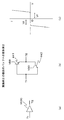
(ドライバICの全体構成)
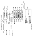
図1は、本発明の実施例1における図6中のドライバIC100の詳細な回路構成を示すブロック図である。
(Overall configuration of driver IC)
FIG. 1 is a block diagram showing a detailed circuit configuration of the
このドライバIC100は、カスケード接続された複数のFF111(=FF111A1〜FF111A25,FF111B1〜FF111B25,FF111C1〜FF111C25,FF111D1〜FF111D25)からなるシフトレジスタ110を有している。シフトレジスタ110は、CLK端子から入力されるクロックHD−CLKに同期して、DATAI3〜DATAI0端子から入力される印刷データHD−DATA3〜HD−DATA0を取り込んでシフトする回路である。
The
ここで、FF111A1〜FF111A25は、カスケード接続されており、ドライバIC100のDATAI0端子はFF111Alのデータ入力用D端子に接続され、FF111A24とFF1111A25のデータ出力用Q端子はセレクタ(SEL)120のデータ入力用端子A0,B0に接続され、セレクタ120のデータ出力用Y0端子がドライバ1C100のデータ出力用DATAO0端子に接続されている。同様に、FF111Bl〜FF111B25、FF111Cl〜FF111C25、及びFF111Dl〜FF111D25も、それぞれカスケード接続されており、ドライバIC100のデータ入力用DATAI1,DATAI2,DATAI3端子が、FF111B1、FF111C1、及びFF111Dlのデータ入力用D端子にそれぞれ接続されている。FF111B24とFF111B25、FF111C24とFF111C25、FF111D24とFF111D25のデータ出力用Q端子も、セレクタ120のデータ入力用A1,A2,A3,B1,B2,B3端子にそれぞれ接続され、セレクタ120のデータ出力用Y1,Y2,Y3端子が、ドライバIC100のデータ出力用DATAO1,DATAO2,DATAO3端子にそれぞれ接続されている。
Here, the FFs 111A1 to FF111A25 are cascade-connected, the DATAI0 terminal of the
これにより、FF111Al〜FF111A25、FF111Bl〜FF111B25、FF111C1〜FF111C25、及びFF111Dl〜FF111D25は、それぞれ25段のシフトレジスタ110を構成しており、セレクタ120により、シフトレジスタ110のシフト段数を24段と25段とに切り替えることが可能な構成になっている。そのため、各ドライバIC100−1,・・・のデータ出力用DATAO0〜DATAO3端子は、次段のドライバ1C100−2,・・・のデータ入力用DATAI0〜DATAI3端子にそれぞれ接続されることになる。従って、ドライバIC100−1〜100−26の全てで構成されるシフトレジスタ110,・・・は、図5の印刷制御部40から初段のドライバ1C100−1中の駆動回路としてのドライバ(DRV)181−1に入力される印刷データHD−DATA3を、クロックHD−CLKに同期してシフトさせる24×26段あるいは25×26段のシフトレジスタを構成している。
Thereby, each of FF111Al to FF111A25, FF111B1 to FF111B25, FF111C1 to FF111C25, and FF111D1 to FF111D25 constitutes a 25-
シフトレジスタ110の出力側には、ラッチ回路部130及びメモリ回路部150の入力側が接続されている。ラッチ回路部130の出力側にはドライバ部180が接続され、メモリ回路部150の入力側に制御回路141が接続され、そのメモリ回路部150の出力側にマルチプレクサ部160が接続されている。マルチプレクサ部160の入力側には、制御回路142が接続されている。ドライバIC100のストローブ信号入力用STB端子には、プルアップ抵抗143及び論理反転用のインバータ144が接続され、更に、ドライバIC100のラッチ信号入力用LOAD端子に、信号反転用のインバータ145が接続されている。インバータ144,145の出力端子には、2入力の否定論理積回路(以下「NAND回路」という。)146の入力端子が接続され、このNAND回路146から出力される駆動オン/オフ制御信号DRVON−Nの出力端子に、ドライバ部180の入力側が接続されている。ドライバ部180の入力側には、駆動量指令手段(例えば、制御電圧発生回路)170も接続されている。
The input side of the
ここで、ラッチ回路部130は、ラッチ信号入力用LOAD端子から入力されるラッチ信号LOAD−P(但し、「−P」は正論理信号を意味する。)により、シフトレジスタ110の出力信号をラッチする回路であり、複数のラッチ回路131(=131A1,131B1,131C1,131D1〜131A24,131B24,131C24,131D24)により構成されている。各ラッチ回路131は、データ入力用D端子、ラッチ信号入力用G端子、及び反転データ出力用QN端子をそれぞれ有し、これらの出力側に、ドライバ部180が接続されている。
Here, the
メモリ回路部150は、制御回路141によりアクセス制御され、発光サイリスタ210の光量ばらつき補正のための補正データ(即ち、ドット補正データ)や各発光素子アレイ200毎の光量補正データ(即ち、チップ補正データ)、もしくは各ドライバIC100毎の固有データを格納するものである。このメモリ回路部150は、複数のメモリ回路151(=151A1,151B1,151C1,151D1〜151A24,151B24,151C24,151D24)とメモリ回路152とにより構成されている。各メモリ回路151は、データ入力用D端子、信号入力用W0〜W3端子、信号入力用E1,E2端子、データ出力用EVN端子、及びODD端子をそれぞれ有している。更に、メモリ回路152は、データ入力用D端子、信号入力用W0〜W3端子、信号入力用E1端子、データ出力用Q0〜Q3端子を有している。このメモリ回路部150の出力側には、マルチプレクサ部160及び制御電圧発生回路170が接続されている。
The
メモリ回路部150を制御する制御回路141は、ラッチ信号入力用LOAD端子、ストローブ信号入力用STB端子、信号出力用W0〜W3端子、及びE1,E2端子を有し、前記補正データを複数のメモリ回路151(=151A1,151B1,151C1,151D1〜151A24,151B24,151C24,151D24)やメモリ回路152に対して書き込みする時の書き込み指令信号をW0〜W3端子、及びE1,E2端子から出力する回路である。
The
マルチプレクサ部160は、制御回路142により制御され、メモリ回路部150中の複数のメモリ回路151(=151A1,151B1,151C1,151D1〜151A24,151B24,151C24,151D24)から出力されるドット補正データにおいて、隣接した発光サイリスタドットの内、奇数番目ドットの補正データと偶数番目ドットの補正データとを切り替えるものであり、複数のマルチプレサ161(=161A1,161B1,161C1,161D1〜161A24,161B24,161C24,161D24)により構成されている。各マルチプレクサ161は、データ入力用EVN端子、ODD端子、信号入力用S1N,S2N端子、及びデータ出力用Q0〜Q3端子をそれぞれ有し、これらの出力側に、ドライバ部180が接続されている。
The
マルチプレクサ部160を制御する制御回路142は、主走査同期信号入力用HSYNC端子、ラッチ信号入力用LOAD端子、及び信号出力用S1N,S2N端子を有し、マルチプレクサ部160に対し奇数番目ドットの補正データと偶数番目ドットの補正データとの切り替え指令信号をS1N,S2N端子から出力する回路である。S1N端子には、ゲート駆動用の共通のバッファ162−1と、共通配線GLと、各ゲート間の電気的な分離を行う分離回路(例えば、レベルシフト機能を有する複数の個別のバッファ)163(=163−1〜163−96)とを介して、奇数番目の各発光サイリスタ210−1,210−3,・・・のゲート駆動用のG1端子がそれぞれ接続されている。更に、S2N端子にも、ゲート駆動用の共通のバッファ162−2と、共通配線GLと、各ゲート間の電気的な分離を行う分離回路(例えば、レベルシフト機能を有する複数の個別のバッファ)164(=164−1〜164−96)とを介して、偶数番目の各発光サイリスタ210−2,210−4,・・・のゲート駆動用のG2端子がそれぞれ接続されている。ゲート駆動用の共通のバッファ162−1及び162−2は、同一の回路構成である。同様に、分離回路として個別のバッファ163(=163−1〜163−96)及び164(=164−1〜164−96)も、同一の回路構成である。
The
ドライバ部180の入力側に接続された制御電圧発生回路170は、データ入力用S0〜S3端子、基準電圧入力用VREF端子、及び制御電圧出力用V端子を備え、例えば、図示しないレギュレータ回路等から発生された基準電圧VREFを入力し、発光サイリスタ駆動のための駆動量指令信号(例えば、制御電圧)VcontをV端子から発生してドライバ部180へ供給する機能を有している。この制御電圧発生回路170は、発光サイリスタ210の全点灯駆動時のように電源電圧VDDが一瞬降下するような状況においても、基準電圧VREFを所定値のままとでき、発光サイリスタ駆動電流の低下を発生させない構成になっている。
The control
ドライバ部180は、ラッチ回路部130、NAND回路146、マルチプレクサ部160、及び制御電圧発生回路170の出力信号に基づき、発光素子アレイ200を駆動するための駆動電流を複数のアノード駆動用DO1〜DO96端子から出力する回路であり、駆動回路としての複数のドライバ181(=181−1〜181−96)により構成されている。各ドライバ181は、データ入力用Q0〜Q3端子、E端子、信号入力用S端子、制御電圧入力用V端子、及び駆動電流出力用DO端子をそれぞれ有している。
The driver unit 180 generates drive currents for driving the light emitting
このドライバ部180の各信号入力用S端子に共通接続されたNAND回路146には、STB端子に入力されるストローブ信号HD−STB−Nと、LOAD端子に入力されるラッチ信号LOAD−Pとが、インバータ144,145を介して入力され、このNAND回路146から駆動オン/オフ制御信号DRVON−Nが出力されてドライバ部180に供給される構成になっている。
The
(図1中のメモリ回路)
図8は、図1中のメモリ回路151の構成を示す回路図である。
(Memory circuit in FIG. 1)
FIG. 8 is a circuit diagram showing a configuration of
図8のメモリ回路151(例えば、151A1)では、発光サイリスタ光量補正のためのドット補正データは4ビットであり、発光サイリスタ駆動電流をドット毎に16段階に調整することで光量補正を行うものとしている。 In the memory circuit 151 (for example, 151A1) in FIG. 8, the dot correction data for light emission thyristor light amount correction is 4 bits, and the light amount correction is performed by adjusting the light emission thyristor drive current in 16 steps for each dot. Yes.
このメモリ回路151A1には、隣接する2個(2ドット)のメモリセル回路300−1,300−2が示されている。左側のメモリセル回路300−1は、奇数番目のドット(例えば、ドットNo.1)の補正データを格納するものであり、右側のメモリセル回路300−2は、偶数番目のドット(例えば、ドットNo.2)の補正データを格納するためのものである。 In the memory circuit 151A1, two adjacent (two dots) memory cell circuits 300-1 and 300-2 are shown. The left memory cell circuit 300-1 stores correction data of odd-numbered dots (for example, dot No. 1), and the right memory cell circuit 300-2 stores even-numbered dots (for example, dot No. 1). This is for storing the correction data of No. 2).
メモリ回路151A1は、シフトレジスタ110中のFF111A1のデータ出力用Q端子から出力される補正データを入力するD端子と、制御手段である制御回路141の端子E1から出力される奇数番目ドットの側のデータ書き込みを許可する書き込みイネーブル信号を入力するE1端子と、制御回路141のE2端子から出力される偶数番目ドットの側のデータ書き込みを許可する書き込みイネーブル信号を入力するE2端子と、制御回路141のW0〜W3端子から出力される書き込み制御信号を入力するW0〜W3端子と、奇数番目ドットに関する補正データを出力するODD0〜ODD3端子と、偶数番目ドットに関する補正データを出力するEVN0〜EVN3端子とを有している。
The memory circuit 151A1 has a D terminal for inputting correction data output from the data output Q terminal of the FF 111A1 in the
補正データ入力用D端子には、入力された補正データを駆動するバッファ301が接続され、このバッファ301に、前記補正データの論理を反転して反転補正データを生成するインバータ302が接続されている。バッファ301の出力端子及びインバータ302の出力端子には、メモリセル回路300−1,300−2が接続されている。
A
メモリセル回路300−1は、メモリ手段(例えば、メモリセル)311〜314と、バッファ301の出力データをメモリセル311〜314へ伝送するスイッチ手段(例えば、NチャネルMOSトランジスタ、以下「NMOS」という。)321〜328と、インバータ302の出力データをメモリセル311〜314へ伝送するスイッチ手段(例えば、NMOS)331〜338とを有している。
The memory cell circuit 300-1 includes memory means (for example, memory cells) 311 to 314 and switch means for transmitting output data of the
メモリセル311は、リング状に直列接続された第1及び第2のインバータ311a,311bにより構成されている。同様に、メモリセル312は、リング状に直列接続されたインバータ312a,312bにより、メモリセル313は、リング状に直列接続されたインバータ313a,313bにより、メモリセル314は、リング状に直列接続されたインバータ314a,314bにより、それぞれ構成されている。各インバータ311a,311b,312a,312b,313a,313b,314a,314bの電源端子は、電源電圧VDD(例えば、一定の略5V)が印加されるVDD端子に接続されている。
The memory cell 311 includes first and
NMOS321,323,325,327のゲートは、書き込みイネーブル信号入力用E1端子に共通に接続され、NMOS322,324,326,328のゲートは、書き込み制御信号入力用W0,W1,W2,W3端子にそれぞれ接続されている。バッファ301の出力端子には、NMOS321,322、補正データ出力用ODD0端子及びメモリセル311の直列回路と、NMOS323,324、補正データ出力用ODD1端子及びメモリセル312の直列回路と、NMOS325,326、補正データ出力用ODD2端子及びメモリセル313の直列回路と、NMOS327,328、補正データ出力用ODD3端子及びメモリセル314の直列回路とが、共通に接続されている。
The gates of the
NMOS331,333,335,337のゲートは、書き込み制御信号入力用W0,W1,W2,W3端子にそれぞれ接続され、NMOS332,334,336,338のゲートは、書き込みイネーブル信号入力用端子E1に共通に接続されている。インバータ302の出力端子には、NMOS332,331及びメモリセル311の直列回路と、NMOS334,333及びメモリセル312の直列回路と、NMOS336,335及びメモリセル313の直列回路と、NMOS338,337及びメモリセル314の直列回路とが、共通に接続されている。
The gates of the
メモリセル回路300−2は、メモリセル回路300−1の書き込みイネーブル信号入力用E1端子に代えて、書き込みイネーブル信号入力用E2端子に接続され、更に、メモリセル回路300−1の補正データ出力用ODD0〜ODD3端子に代えて、補正データ出力用EVN0〜EVN3端子に接続されている他は、メモリセル回路300−1と同様の構成である。 The memory cell circuit 300-2 is connected to the write enable signal input E2 terminal in place of the write enable signal input E1 terminal of the memory cell circuit 300-1, and is further connected to the correction data output of the memory cell circuit 300-1. The configuration is the same as that of the memory cell circuit 300-1, except that the correction data output EVN0 to EVN3 terminals are connected in place of the ODD0 to ODD3 terminals.
(図1中のマルチプレクサ)
図9は、図1中のマルチプレクサ161の構成を示す回路図である。
(Multiplexer in Fig. 1)
FIG. 9 is a circuit diagram showing a configuration of
図9のマルチプレクサ161(例えば、161A1)は、メモリ回路151A1のODD0〜ODD3端子から出力される補正データODD0〜ODD3を入力するODD0端子〜ODD3端子と、メモリ回路151A1のEVN0〜EVN3端子から出力される補正データEVN0〜EVN3を入力するEVN0〜EVN3端子と、制御回路142のS1N端子及びS2N端子から出力される奇数ドットデータと偶数ドットデータとの切り替え指令信号S1N,S2Nを入力するS1N,S2N端子と、補正データQ0〜Q3を出力するQ0〜Q3端子と、入力データ切り替え用のPチャネルMOSトランジスタ(以下「PMOS」という。)341〜348とを有している。
The multiplexer 161 (for example, 161A1) in FIG. 9 is output from the ODD0 to ODD3 terminals for inputting the correction data ODD0 to ODD3 output from the ODD0 to ODD3 terminals of the memory circuit 151A1 and the EVN0 to EVN3 terminals of the memory circuit 151A1. EVN0 to EVN3 terminals to input correction data EVN0 to EVN3, and S1N and S2N terminals to input switching command signals S1N and S2N between odd dot data and even dot data output from the S1N terminal and S2N terminal of the
PMOS341,343,345,347は、S1N端子から入力される切り替え指令信号S1Nによりゲート制御され、入力側のODD0〜ODD3端子と出力側のQ0〜Q3端子との間をそれぞれオン/オフする構成になっている。更に、PMOS342,344,346,348は、S2N端子から入力される切り替え指令信号S2Nによりゲート制御され、入力側のEVN0〜EVN3端子と出力側のQ0〜Q3端子との間をそれぞれオン/オフする構成になっている。
The
このようなマルチプレクサ161の構成において、スイッチ素子としてPMOS341〜348を用いているのは次の理由によるものであって、動作上の支障を防止しつつ、使用される素子数を削減することが可能な構成となっている。
In such a configuration of the
即ち、PMOS341をオンさせるために切り替え指令信号S1Nを低レベル(以下「Lレベル」という。)にする時、補正データODD0がHレベルであれば、この補正データODD0のHレベルと略等しい電圧の補正データQ0が出力される。このようにHレベルの伝達であれば、PMOS341をスイッチ素子として使用した場合でも何ら支障がない。
That is, when the switching command signal S1N is set to a low level (hereinafter referred to as “L level”) to turn on the
一方、補正データODD0がLレベル(≒0V)であったとすると、PMOS341の第2端子であるドレーンは、このPMOS341の閾値電圧に近い電位にまで降下するものの、Lレベル(≒0V)にまで下がることはなく、Lレベルの伝達機能が完全ではない欠点を内在している。
On the other hand, if the correction data ODD0 is at the L level (≈0V), the drain as the second terminal of the
このような欠点を解消するため、本実施例1に対する比較例による構成においては、例えば、PMOSと並列にNMOSを接続したアナログスイッチを構成してデータ選択のためのスイッチ手段としている。この構成においては、伝達しようとする入力電圧と略等しい出力電圧を得ることができ、スイッチ手段が介在していることによる入力電圧と出力電圧の差は生じない。しかし、データ線1本当たりにPMOSとNMOSのトランジスタ対を設ける必要があり、図9の構成に比べて2倍の素子数を要し、それを配置するためのICのチップ面積を多く占有するという欠点を内在している。 In order to eliminate such drawbacks, in the configuration according to the comparative example with respect to the first embodiment, for example, an analog switch in which NMOS is connected in parallel with PMOS is configured as switch means for data selection. In this configuration, an output voltage substantially equal to the input voltage to be transmitted can be obtained, and there is no difference between the input voltage and the output voltage due to the presence of the switch means. However, it is necessary to provide a pair of PMOS and NMOS transistors per data line, which requires twice the number of elements as compared to the configuration of FIG. 9, and occupies a large chip area of the IC for arranging them. The inherent disadvantage is.
これに対し、本実施例1の図9の構成では、比較例のアナログスイッチを用いて構成した回路と比べて、半分の素子数で済むという利点を有しているものの、Lレベルの伝達機能が完全ではないという欠点を内在している。ところが、後述するように、マルチプレクサ161の出力側に接続される後段のドライバ181においては、Hレベルとして略電源電圧VDDと等しい入力電圧を要するのに対し、Lレベルとしては後述する制御電圧Vcontの電位にまで下降していれば十分であり、略0Vにまで電位降下するようなLレベル電位を必要としていない。そのため、図9に示すマルチプレクサ回路を用いることで、回路動作上の制約を回避しつつ、所要素子数を削減することができる。
On the other hand, the configuration of FIG. 9 of the first embodiment has an advantage that only half the number of elements is required as compared with the circuit configured by using the analog switch of the comparative example, but the L level transmission function. Has the inherent disadvantage of not being perfect. However, as will be described later, the
(図1中のドライバ)
図10は、図1中のドライバ181の構成を示す回路図である。
(Driver in Fig. 1)
FIG. 10 is a circuit diagram showing a configuration of
図10のドライバ181(例えば、181−93)は、ラッチ回路131A1の反転出力用端子QNから出力される負論理の印刷データを入力する端子Eと、NAND回路146から出力される負論理の駆動オン/オフ制御信号DRVON−Nを入力するS端子と、マルチプレクサ161A1のQ0〜Q3端子から出力される補正データQ0〜Q3を入力するQ0端子〜Q3端子と、制御電圧発生回路170のV端子から出力される制御電圧Vcontを入力するV端子と、電源電圧VDDが入力されるVDD端子と、図示しない薄膜配線により接続された発光サイリスタ210のアノードに対して駆動電流を供給するDO端子(=DO93端子)とを有している。
The driver 181 (for example, 181 to 93) in FIG. 10 drives a terminal E for inputting negative logic print data output from the inverted output terminal QN of the latch circuit 131A1 and a negative logic drive output from the
E端子及びS端子は、2入力の否定論理和回路(以下「NOR回路」という。)350の入力端子に接続されている。NOR回路350は、電源端子がVDD端子に接続され、グランド端子がV端子に接続されて制御電圧Vcontに保持されている。NOR回路350の出力端子とQ0〜Q3端子とは、2入力NAND回路351〜354の入力端子にそれぞれ接続されている。各NAND回路351〜354は、電源端子がVDD端子に接続され、グランド端子がV端子に接続されて制御電圧Vcontに保持されている。更に、NOR回路350の出力端子は、CMOSインバータ355を構成するPMOS355a及びNMOS355bの各ゲートに共通に接続されている。PMOS355a及びNMOS355bは、VDD端子とV端子との間に直列に接続されている。
The E terminal and the S terminal are connected to an input terminal of a two-input NAND circuit (hereinafter referred to as “NOR circuit”) 350. In the NOR
NAND回路351〜354の出力端子には、PMOS356〜359のゲートがそれぞれ接続され、更に、CMOSインバータ355の出力端子に、PMOS360のゲートが接続されている。各PMOS356〜360の第1端子であるソース及び第2端子であるドレーンは、VDD端子とDO端子との間に並列に接続されている。PMOS360は、発光サイリスタ210のアノードに主たる駆動電流を供給する主駆動トランジスタであり、PMOS356〜359は、発光サイリスタ210の駆動電流をドット毎に調整して光量補正するための補助駆動トランジスタである。
The gates of
ここで、VDD端子の電位と、V端子から入力される制御電圧Vcontの電位との電位差は、PMOS356〜360がオンする時のゲート・ソース間電圧に略等しく、この電圧を変化させることで、PMOS356〜360のドレーン電流を調整することが可能となる。制御電圧Vcontを供給するための図1中の制御電圧発生回路170は、基準電圧VREFを受けて、PMOS356〜360等のドレーン電流が所定値となるように制御電圧Vcontを制御するために設けられている。
Here, the potential difference between the potential of the VDD terminal and the potential of the control voltage Vcont input from the V terminal is substantially equal to the gate-source voltage when the
このように構成されるドライバ181−93は、次のように動作する。
E端子に入力される印刷データがオン(=Lレベル)であり、S端子に入力される駆動オン/オフ制御信号DRVON−Nがオン(=Lレベル)の時、NOR回路350の出力信号がHレベルとなる。この時、Q3〜Q0端子の補正データQ3〜Q0に従い、NAND回路351〜354の出力レベル、及びCMOSインバータ355の出力レベルが、電源電圧VDDあるいは制御電圧Vcontとなる。
The driver 181-93 configured as described above operates as follows.
When the print data input to the E terminal is ON (= L level) and the drive ON / OFF control signal DRVON-N input to the S terminal is ON (= L level), the output signal of the NOR
主駆動用のPMOS360は、E端子に入力される印刷データに従って駆動される。図8のメモリ回路151A1には、発光サイリスタ210の各ドットの発光ばらつきを補正するための補正データQ0〜Q3が格納されているので、この補正データQ0〜Q3が、マルチプレクサ161A1のQ0〜Q3端子から出力される。補助駆動用のPMOS356〜359は、NOR回路350の出力レベルがHレベルである時に、マルチプレクサ161A1のQ0〜Q3端子から出力される補正データQ0〜Q3に従って選択的に駆動される。
The
つまり、主駆動用のPMOS360と共に、補正データQ0〜Q3に従って補助駆動用のPMOS356〜359が選択的に駆動され、PMOS360のドレーン電流に対し、選択されたPMOS356〜359の各ドレーン電流が加算された駆動電流が、DO93端子から発光サイリスタ210のアノードに供給される。
That is, the auxiliary driving
PMOS356〜359が駆動されている時、NAND回路351〜354の出力レベルはLレベル(≒制御電圧Vcont)であるので、PMOS356〜359のゲート電圧は、略制御電圧Vcontに等しくなる。この時、PMOS355aはオフ状態にあり、NMOS355bはオン状態にあって、PMOS360のゲート電圧もまた略制御電圧Vcontに等しくなる。そのため、PMOS356〜360のドレーン電流値を、制御電圧Vcontにより一括して調整することができる。この際、NAND回路351〜354は、電源端子に電源電圧VDD、及びグランド端子に制御電圧Vcontが印加されて動作しているので、その入力信号の電圧も電源電圧VDDと制御電圧Vcontに即したものであってよく、Lレベルは必ずしも0Vであることを必要としない。従って、図9に示す構成のマルチプレクサ161を用いても、支障なく動作させることができる。
When the
(図1中の制御回路141)
図11は、図1中の制御回路141の構成を示す回路図である。
(
FIG. 11 is a circuit diagram showing a configuration of
この制御回路141は、正論理のラッチ信号LOAD−Pを入力するLOAD端子と、図1中のインバータ144から出力される正論理のストローブ信号STB−Pを入力するSTB端子と、書き込み制御信号W0〜W3を図1中のメモリ回路部150へ出力するW0〜W3端子と、書き込みイネーブル信号E1,E2をメモリ回路部150へ出力するE1,E2端子と、FF361〜365と、2入力のNOR回路366と、2入力の論理積回路(以下「AND回路」という。)367,368と、3入力のAND回路370〜373とを備えている。
The
各FF361,362は、LOAD端子から入力されるラッチ信号LOAD−Pを入力する負論理リセット用R端子と、STB端子から入力されるストローブ信号STB−Pを入力するクロック入力用CK端子と、データ入力用D端子と、非反転データ出力用Q端子とを有している。各FF363〜365は、LOAD端子から入力されるラッチ信号LOAD−Pを入力する負論理リセット用R端子と、クロック入力用CK端子と、データ入力用D端子と、非反転データ出力用Q端子と、反転データ出力用QN端子とを有している。
Each of the
FF361,362のQ端子は、NOR回路366の入力端子と接続され、このNOR回路366の出力端子がFF361のD端子に接続されている。FF361のQ端子は、FF363のCK端子に接続され、このFF363のQN端子がD端子に接続されている。FF363のQ端子とLOAD端子とは、AND回路367の入力端子に接続され、このAND回路367の出力端子がE1端子に接続されている。FF363のQN端子とLOAD端子とは、AND回路368の入力端子に接続され、このAND回路368の出力端子がE2端子に接続されている。
The Q terminals of the
AND回路367の出力端子は、FF364,365のCK端子に接続され、このFF364,365のR端子が、LOAD端子に接続されている。FF364のQN端子は、FF365のD端子に接続されている。FF364,365のQ端子及びQN端子とFF362のQ端子とには、AND回路370〜373の入力端子が接続され、このAND回路370〜373の出力端子が、W0〜W3端子に接続されている。
The output terminal of the AND
即ち、AND回路373の第1入力端子はFF365のQ端子、及び第2入力端子はFF364のQN端子にそれぞれ接続され、AND回路372の第1入力端子はFF365のQ端子、及び第2入力端子はFF364のQ端子にそれぞれ接続され、AND回路371の第1入力端子はFF365のQN端子、及び第2入力端子はFF364のQ端子にそれぞれ接続され、AND回路370の第1入力端子はFF365のQN端子、及び第2入力端子はFF364のQN端子にそれぞれ接続されている。
That is, the first input terminal of the AND
(図1中の制御回路142)
図12は、図1中の制御回路142の構成を示す回路図である。
(
FIG. 12 is a circuit diagram showing a configuration of
この制御回路142は、FF381及びバッファ382,383を有している。FF381は、HSYNC端子からの負論理の主走査同期信号HSYNC−Nを入力する負論理のリセット用R端子と、LOAD端子からの正論理のラッチ信号LOAD−Pを入力するクロック入力用CK端子と、相互に接続されたデータ入力用D端子及び反転データ出力用QN端子と、非反転データ出力用Q端子とを有し、これらのQ端子及びQN端子が、バッファ382,383を介して切り替え指令信号用S2N,S1N端子にそれぞれ接続されている。
The
この制御回路142では、CK端子に入力されるラッチ信号LOAD−Pに同期して、H又はLの切り替え指令信号S1N,S2NをS1N端子及びS2N端子から出力する構成になっている。
The
(図1中の制御電圧発生回路)
図13は、図1中の制御電圧発生回路170の構成を示す回路図である。
(Control voltage generation circuit in FIG. 1)
FIG. 13 is a circuit diagram showing a configuration of control
この制御電圧発生回路170は、ドライバIC100毎に1回路ずつ設けられ、演算増幅器(以下「オペアンプ」という。)391と、PMOS392と、直列接続された分圧抵抗R00〜R15からなる分圧回路393と、アナログ形のマルチプレクサ394とにより構成されている。
The control
オペアンプ391は、反転入力端子が基準電圧入力用VREF端子に接続され、非反転入力端子がマルチプレクサ394の出力用Y端子に接続され、出力端子がPMOS392のゲート及び制御電圧出力用V端子に接続されている。PMOS392は、図10中の各PMOS356〜360とゲート長が等しく、ソースがVDD端子に接続され、ゲートがオペアンプ391の出力端子及びV端子に接続され、ドレーンが分圧回路393を介してグランドGNDに接続されている。
The
マルチプレクサ394は、直列接続された分圧抵抗R15〜R00における各接続点からのアナログ電圧が入力される16個の入力用P0〜P15端子と、アナログ電圧を出力する出力用Y端子と、図1中のメモリ回路152の出力用Q0〜Q3端子から供給される論理信号S0〜S3が入力される4個の入力用S0〜S3端子とを有し、この4本の論理信号S0〜S3により設定される16通りの信号論理の組み合わせによって、入力用P0〜P15端子の内の何れか1つの端子を選択し、この端子に印加されるアナログ電圧をY端子からオペアンプ391の非反転入力端子へ出力する回路である。換言すれば、マルチプレクサ393における入力用S3〜S0端子の論理信号レベルによって、入力用P0〜P15端子の内の何れか1つの端子が選択され、出力用Y端子との間に電流経路が形成される。
The
オペアンプ391と分圧抵抗R00〜R15及びPMOS392とで構成される回路により、フィードバック制御回路が構成され、オペアンプ391の非反転入力端子の電位が、略基準電圧VREFと等しくなるように制御される。このため、PMOS392のドレーン電流Irefは、分圧抵抗R00〜R15の内、マルチプレクサ394により選択される部位の合成抵抗値と、オペアンプ391に入力される基準電圧VREFとから決定されることになる。
A feedback control circuit is configured by a circuit including the
例えば、マルチプレクサ394の入力用S3〜S0端子の論理値が“1111”となっていて、補正状態の最大が指令されている時、マルチプレクサ394の入力用P15端子と出力用Y端子とが導通状態になり、入力用P15端子の電圧が基準電圧VREFと略等しくなるように制御される。この結果、PMOS392のドレーン電流Irefは、
Iref=VREF/R00
となる。
For example, when the logical value of the input S3 to S0 terminals of the
Iref = VREF / R00
It becomes.
一方、入力用S3〜S0端子の論理値が“0111”となっていて、補正状態の中間が指令されている時、マルチプレクサ394の入力用P7端子と出力用Y端子とが導通状態になり、入力用P7端子の電圧が基準電圧VREFと略等しくなるように制御される。この結果、PMOS392のドレーン電流Irefは、
Iref=VREF/(R00+R01+・・・+R07+R08)
となる。
On the other hand, when the logical values of the input S3 to S0 terminals are “0111” and the middle of the correction state is commanded, the input P7 terminal and the output Y terminal of the
Iref = VREF / (R00 + R01 +... + R07 + R08)
It becomes.
更に、入力用S3〜S0端子の論理値が“0000”となっていて、補正状態の最小が指令されている時、マルチプレクサ394の入力用P0端子と出力用Y端子とが導通状態となり、入力用P0端子の電圧が前記基準電圧VREFと略等しくなるように制御される。この結果、PMOS392のドレーン電流Irefは、
Iref=VREF/(R00+R01+・・・+R14+R15)
となる。
Further, when the logical value of the input S3 to S0 terminals is “0000” and the minimum correction state is instructed, the input P0 terminal and the output Y terminal of the
Iref = VREF / (R00 + R01 +... + R14 + R15)
It becomes.
このように、図10中のPMOS356〜360と図13中のPMOS392とは、ゲート長が相等しく構成され、これらPMOSが飽和領域で動作するように制御されているので、各PMOSはカレントミラーの関係となり、PMOS356〜360がオン状態となる時、基準電圧VREFに比例するドレーン電流Irefを生じる。この結果、マルチプレクサ394の入力用S3〜S0端子に与える論理値状態により、ドレーン電流Irefを16段階に調整することができ、図10中のPMOS356〜360のドレーン電流もまた16段階に調整可能とすることができる。
As described above, the
(図1中の個別のバッファ)
図14(a)〜(d)は、図1中の個別のバッファ163の構造を示す模式図であり、同図(a)は回路シンボルを示す図、同図(b)は同図(a)の回路構成を示す図、同図(c)は同図(b)の回路をICとして実現したときの概略の断面構造を示す図、及び、同図(d)は同図(b)、(c)の電圧/電流特性を示す図である。
(Individual buffers in Fig. 1)
14A to 14D are schematic views showing the structure of the
図14(a)に示すように、個別のバッファ163は、第3端子(例えば、入力側の第1端子)T1及び第4端子(出力側の第2端子)T2を有している。
As shown in FIG. 14A, the
なお、図1中の他の個別のバッファ164は、バッファ163と同一の回路構成であるので、以下、バッファ163についてのみ説明する。
Since the other
図14(b)に示すように、個別のバッファ163は、例えば、第1トランジスタ(例えば、NPNTR401と第2トランジスタ(例えば、NPNTR)402とを有し、これらが入力側の第1端子T1と出力側の第2端子T2との間に逆並列状態に接続されている。即ち、NPNTR401のコレクタ及びベースとNPNTR402のエミッタとは、第1端子T1に接続され、NPNTR401のエミッタとNPNTR402のコレクタ及びベースとが、第2端子T2に接続されている。このバッファ163は、第1端子T1及び第2端子T2間に印加される印加電圧の絶対値が所定電圧以上となると、この印加電圧の極性に応じた向きの電流を生じる特性を有している。
As shown in FIG. 14B, the
図14(c)に示すように、IC等が形成されているP型不純物を含んだP型基材410上の所定箇所には、N型不純物を注入してNウェル領域411が形成されている。Nウェル領域411内には、P型不純物を注入してPウェル領域412が形成され、更に、そのPウェル領域412内に、N型不純物を拡散させてN型領域413が形成されている。
As shown in FIG. 14C, an
なお、図14(c)においては図面を簡略化するために、ゲート酸化膜、コンタクトホール、保護膜であるパッシベーション膜等の図示を省略している。図示しない金属配線により、N型領域413がエミッタEに、Pウェル領域412がベースBに、Nウェル領域411がコレクタCにそれぞれ接続され、NPNTR401又は402が構成されている。
In FIG. 14C, illustration of a gate oxide film, a contact hole, a passivation film as a protective film, and the like is omitted to simplify the drawing. The
図14(d)に示すバッファ163の電圧/電流特性図において、横軸は図14 (b)の第1端子T1と第2端子T2間に印加される電圧(V)、縦軸は第1端子T1と第2端子T2間に流れる電流(I)を示している。この特性図から明らかなように、第1端子T1と第2端子T2間に印加される電圧Vの絶対値が電圧Vfを越えると、電流Iが流れる特性となっている。その電圧Vfは、NPNTR401,402のベース・エミッタ間の順電圧(即ち、ベース・エミッタ間電圧Veb)に等しく、図14(c)のバッファ163をシリコン基材を用いて形成した場合における電圧Vfの典型例は、約0.6Vである。
In the voltage / current characteristic diagram of the
(プリントヘッドの全体の動作)
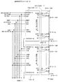
図15は、本発明の実施例1における画像形成装置1の電源投入後に、図6のプリントヘッド13に対して行われる補正データ転送処理と、その後に行われる印刷データ転送の様子を概略的に示すタイミングチャートである。
(Overall operation of print head)
FIG. 15 schematically shows a correction data transfer process performed on the
補正データの転送開始に先立ち、引き続くデータ転送が補正データであることを示すため、ラッチ信号HD−LOADをHレベルとする(I部)。 Prior to the start of transfer of correction data, the latch signal HD-LOAD is set to H level (section I) to indicate that the subsequent data transfer is correction data.
次いで、奇数番目に属するドットについて1ドット当たり4ビットからなる補正データの内、bit3のものを印刷データHD−DATA3〜HD−DATA0からクロックHD−CLKに同期して入力して、図1のFF111A1〜FF111D24で構成されるシフトレジスタ110中へシフト入力する。シフト入力が完了すると、A部に示すように、ストローブ信号HD−STB−Nが3パルス入力され、図11の制御回路141の動作が行われる。
Next, among the correction data consisting of 4 bits per dot for the odd numbered dots, the
図15中のQ1,Q2,Q3,Q4,Q5は、図11中のFF361,362,363,365,364の各出力端子であり、E1,E2は、AND回路367,368から出力される書き込みイネーブル信号であり、W3〜W0は、AND回路370〜373から出力される書き込み制御信号である。更に、SlN,S2Nは、図12中のバッファ382,383から出力される奇数ドットデータと偶数トッドデータとの切り替え指令信号である。
15, Q1, Q2, Q3, Q4, and Q5 are output terminals of the
図15のA部において、ストローブ信号HD−STB−Nの1パルス目が入力されると、J部に示すように、Q1端子の信号が発生し、次いでストローブ信号HD−STB−Nの2パルス目で、K部に示すように、Q2端子の信号が発生する。又、Q1端子の信号が立ち上がる毎にQ3端子の信号が状態反転し、L部に示すように、Q3端子の信号がHレベルに遷移する。Q3端子の信号の遷移に引き続き、書き込みイネーブル信号E1,E2が発生する。 In the A part of FIG. 15, when the first pulse of the strobe signal HD-STB-N is inputted, as shown in the J part, a signal of the Q1 terminal is generated, and then two pulses of the strobe signal HD-STB-N are generated. At first, as shown in the K section, a signal at the Q2 terminal is generated. Further, every time the signal at the Q1 terminal rises, the signal at the Q3 terminal is inverted, and the signal at the Q3 terminal transitions to the H level as shown in the L part. Following the transition of the signal at the Q3 terminal, write enable signals E1 and E2 are generated.
書き込みイネーブル信号E1の立ち上がりエッジに引き続き、M部に示すように、Q4端子の信号が立ち上がり、書き込みイネーブル信号E1の次の立ち上がりで、Q5端子の信号が立ち上がり、更に、書き込みイネーブル信号Elの次の立ち上がりで、Q4端子の信号が立ち下がり、書き込みイネーブル信号Elの次の立ち上がりで、Q5端子の信号が立ち下がる。 Subsequent to the rising edge of the write enable signal E1, the signal at the Q4 terminal rises, the signal at the Q5 terminal rises at the next rise of the write enable signal E1, and then the next of the write enable signal El. At the rising edge, the signal at the Q4 terminal falls, and at the next rising edge of the write enable signal El, the signal at the Q5 terminal falls.
書き込み制御信号W3〜W0は、Q2端子の信号に引き続いて発生するものであるが、O部、P部に示すように、書き込み制御信号W3が2回に亘って出力され、次いで、各書き込み制御信号W2,Wl,W0においても、それぞれ2パルスずつ発生する。 The write control signals W3 to W0 are generated subsequent to the signal of the Q2 terminal. As shown in the O part and the P part, the write control signal W3 is output twice, and then each write control signal is output. Each of the signals W2, W1, and W0 also generates two pulses.
各書き込み制御信号W3〜W0のパルスが発生する毎に、図8のメモリ回路151にデータの書き込みが行われ、書き込み制御信号W3〜W0の1パルス目で、メモリセル回路300−1内の奇数ドット用メモリセル311〜314へのデータ書き込みが行われ、2パルス目で、メモリセル回路300−1内の偶数ドット用メモリセルへのデータ書き込みが行われる。
Data is written to the
前記1パルス目の書き込み制御信号W3〜W0(O部等)は、A部、C部、E部、G部について入力されたストローブ信号HD−STB−Nを基に発生されるものであり、前記2パルス目の書き込み制御信号W3〜W0(P部等)は、B部、D部、F部、H部について入力されたストローブ信号HD−STB−Nを基に発生されるものである。 The first pulse write control signals W3 to W0 (such as the O portion) are generated based on the strobe signal HD-STB-N input to the A portion, the C portion, the E portion, and the G portion. The second pulse write control signals W3 to W0 (P portion, etc.) are generated based on the strobe signal HD-STB-N input to the B portion, D portion, F portion, and H portion.
以上の過程を経て、補正データb3〜b0(Odd=ODD3〜ODD0,Even=EVN3〜EVN0)のbit3〜bit0の全てのデータ書き込みが完了すると、Q部に示すように、ラッチ信号HD−LOADをLレベルにして、印刷データHD−DATA3〜HD−DATA0の転送が可能な状態に遷移する。1ラインの印刷開始に際し、引き続くデータ転送が奇数ドットのものであることを示すため、主走査同期信号HD−HSYNC−Nが入力される(R部)。
Through the above process, when all the data writing of
次いで、U部で奇数ドットの印刷データHD−DATA3〜HD−DATA0が転送され、S部のラッチ信号HD−LOADのパルスにより、シフトレジスタ110にシフト入力された印刷データHD−DATA3〜HD−DATA0が、ラッチ部130にラッチされる。
Next, the odd-dot print data HD-DATA3 to HD-DATA0 are transferred in the U portion, and the print data HD-DATA3 to HD-DATA0 shifted to the
更に、W部に示すように、ストローブ信号HD−STB−NがLレベルへと遷移して、発光サイリスタ210−1,210−2,・・・の発光駆動が行われる。印刷データHD−DATA3〜HD−DATA0がオン状態であると、W部やX部のストローブ信号HD−STB−NがLレベルとなる期間、発光サイリスタ210−1,210−2,・・・が発光駆動されることになる。 Further, as shown in the W section, the strobe signal HD-STB-N transitions to the L level, and the light emission thyristors 210-1, 210-2,. When the print data HD-DATA3 to HD-DATA0 are in the ON state, the light-emitting thyristors 210-1, 210-2,... Are output during the period when the strobe signal HD-STB-N of the W part and the X part is at the L level. The light emission is driven.
同様にV部では、偶数ドットのデータ転送が行われ、このデータはT部のパルスによりラッチされる。なお、図1に示すように、制御回路142から出力される切り替え指令信号S1Nは、図1のバッファ162−1,163(=163−1〜163−96)を介してゲート駆動信号G1となり、奇数番目の発光サイリスタ210−1,210−3,・・・のゲートが駆動される。更に、制御回路142から出力される切り替え指令信号S2Nは、図1のバッファ162−2,164(=164−1〜164−96)を介してゲート駆動信号G2となり、偶数番目の発光サイリスタ210−2,210−4,・・・のゲートが駆動される。
Similarly, even-dot data transfer is performed in the V portion, and this data is latched by the pulse in the T portion. As shown in FIG. 1, the switching command signal S1N output from the
(プリントヘッドの印刷動作)
図16は、図6のプリントヘッド13を用いて印刷を行う場合の動作を示すタイミングチャートである。
(Print head printing operation)
FIG. 16 is a timing chart showing an operation when printing is performed using the
発光サイリスタ210の時分割駆動の開始に先立ち、主走査同期信号HD−HSYNC−Nが入力される(A部)。次いでB部において、奇数番目の発光サイリスタ210−1,210−3,・・・の駆動データ(0dd印刷データ)を転送するため、クロックHD−CLKに同期して印刷データHD−DATA3〜HD−DATA0が入力される。なお、本プリントヘッド13においては26個のドライバIC100(=100−1,100−2,・・・)がカスケードに接続され、各ドライバIC100毎に96個の発光サイリスタ駆動用の端子DO1〜DO96を備えており、1パルスのクロックHD−CLKにより、4画素分の印刷データHD−DATA3〜HD−DATA0が一度に転送される。このため、一度のデータ転送に必要なクロックパルス数は、
96/4*26=24*26=624
である。
Prior to the start of time-division driving of the light-emitting
96/4 * 26 = 24 * 26 = 624
It is.
B部において、1ラインデータのうち、奇数ドットのデータの転送が完了すると、C部に示すように、ラッチ信号HD−LOADが入力され、FF111A1,111B1,111C1,111D1〜111A25,111B25,111C25,111D25で構成されるシフトレジスタ110を介して入力された印刷データHD−DATA3〜HD−DATA0は、ラッチ回路部130にラッチされる。この時、発光サイリスタ210のゲート駆動信号G1がLレベルとなり(L部)、ゲート駆動信号G2がHレベルとされる(N部)。
When transfer of odd-numbered dots of one line data is completed in the B section, the latch signal HD-LOAD is input as shown in the C section, and the FFs 111A1, 111B1, 111C1, 111D1 to 111A25, 111B25, 111C25, The print data HD-DATA3 to HD-DATA0 input via the
次いで、発光サイリスタ210の駆動を指示するためのストローブ信号HD−STB−Nが入力される(D部)。これにより、ドライバIC100(=100−1,100−2,・・・)のD01〜D096端子は、印刷データHD−DATA3〜HD−DATA0による指令値に基づき選択的にオン状態となって、駆動電流が出力される(Q部)。この時、駆動される発光サイリスタ210は、G1端子がゲートに接続される奇数番目の発光サイリスタ210−1,210−3,・・・である。このため、ドライバIC100のDO1端子から駆動電流が出力された場合、発光サイリスタ210−1のアノード・カソードを経てグランドGNDへと至る電流経路が形成される。
Next, a strobe signal HD-STB-N for instructing driving of the
一方、発光サイリスタ210−2は、ゲートのレベルがHレベルとなっていてオフ状態とされ、ドライバIC100のDO1端子からの駆動電流が流れず、消灯状態のままとされる。この結果、発光サイリスタ210−1が発光して、図2中の感光体ドラム11上の静電潜像を形成することで、印刷ドットを発生する。
On the other hand, the light emitting thyristor 210-2 is turned off because the gate level is H level, the drive current from the DO1 terminal of the
F部において、負論理のストローブ信号HD−STB−NがHレベルとなると、ドライバIC100による駆動はオフ状態となって、発光サイリスタ210−1,210−2,・・・がすべて消灯される(R部)。
When the negative logic strobe signal HD-STB-N becomes H level in the F section, the driving by the
更に、E部において、偶数番目の発光サイリスタ210−2,210−4,・・・の駆動データ(Even印刷データ)を転送するために、クロックHD−CLKに同期して印刷データHD−DATA3〜HD−DATA0が入力される。なお、本プリントヘッド13においては、26個のドライバIC100(=100−1,100−2,・・・)がカスケードに接続され、各ICドライバ100毎に96個の発光サイリスタ駆動用の端子DO1〜DO96を備えており、1パルスのクロックHD−CLKにより、4画素分の印刷データHD−DATA3〜HD−DATA0が一度に転送されるため、一度のデータ転送に必要なクロックパルス数は、
96/4*26=24*26=624
である。
Further, in the E section, in order to transfer the drive data (even print data) of the even-numbered light emitting thyristors 210-2, 210-4,..., The print data HD-DATA3 is synchronized with the clock HD-CLK. HD-DATA0 is input. In this
96/4 * 26 = 24 * 26 = 624
It is.
E部において、1ラインデータの内、偶数ドットのデータ(Even印刷データ)の転送が完了すると、G部に示すように、ラッチ信号HD−LOADが入力され、シフトレジスタ110を介して入力されたデータがラッチ回路部130にラッチされる。この時、発光サイリスタ210のゲート駆動信号G1がHレベルとなり(M部)、ゲート駆動信号G2がLレベルとされる(0部)。
When transfer of even dot data (Even print data) in one line data is completed in the E section, the latch signal HD-LOAD is input and input via the
次いで、発光サイリスタ210の駆動を指示するためのストローブ信号HD−STB−Nが入力される(H部)。これにより、ドライバIC100(=100−1,100−2,・・・)のDO1〜DO96端子は、印刷データHD−DATA3〜HD−DATA0による指令値に基づき選択的にオン状態となって、駆動電流が出力される(S部)。この時駆動される発光サイリスタ210は、G2端子がゲートに接続される偶数番目の発光サイリスタ210−2,210−4,・・・である。このため、ドライバIC100のDO1端子から駆動電流が出力された場合、発光サイリスタ210−2のアノード・カソードを経てグランドGNDへと至る電流経路が形成されることになる。
Next, a strobe signal HD-STB-N for instructing driving of the
一方、発光サイリスタ210−1は、ゲートのレベルがHレベルとなっていてオフ状態とされ、ドライバIC100のDO1端子からの駆動電流が流れず、消灯状態のままとされる。この結果、発光サイリスタ210−2が発光して、図2中の感光体ドラム11上の静電潜像を形成することで印刷ドットを発生する。
On the other hand, the light emitting thyristor 210-1 is turned off because the gate level is at the H level, the drive current from the DO1 terminal of the
J部において、負論理のストローブ信号HD−STB−NがHレベルとなると、ドライバIC100による駆動はオフ状態となって、発光サイリスタ210−1,210−2,・・・がすべて消灯される(T部)。
When the negative logic strobe signal HD-STB-N becomes H level in the J section, the driving by the
このように、発光サイリスタ列のうち、奇数番目の発光サイリスタ210−1,210−3,・・・と偶数番目の発光サイリスタ210−2,210−4,・・・とを順に時分割に駆動することで、1ライン分の発光サイリスタ210−1,210−2,・・・の駆動を行うことができる。 In this way, the odd-numbered light-emitting thyristors 210-1, 210-3,... And the even-numbered light-emitting thyristors 210-2, 210-4,. By doing so, it is possible to drive the light emitting thyristors 210-1, 210-2,... For one line.
(補正データ転送の詳細)
図17〜図20は、図15のタイミングチャートにおいてドライバ1C100(=100−1,100−2,・・・)を1チップのみに簡略化した場合における補正データ転送の詳細波形を示すタイミングチャートである。
(Details of correction data transfer)
17 to 20 are timing charts showing detailed waveforms of correction data transfer when the driver 1C100 (= 100-1, 100-2,...) Is simplified to only one chip in the timing chart of FIG. is there.
ここで、図17は図15のA部とB部の詳細を示すタイミングチャート、図18は図15のC部とD部の詳細を示すタイミングチャート、図19は図15のE部とF部の詳細を示すタイミングチャート、更に、図20は図15のG部とH部の詳細を示すタイミングチャートである。 Here, FIG. 17 is a timing chart showing details of A and B parts in FIG. 15, FIG. 18 is a timing chart showing details of C and D parts in FIG. 15, and FIG. 19 is E parts and F parts in FIG. FIG. 20 is a timing chart showing details of the G and H parts in FIG.
図15において、各ドライバ1C100毎に設定されるチップ補正データb3〜b0は、奇数ドット転送(例えば、A部)と偶数ドット転送(例えば、B部)の内、いずれか1回について行えば十分である。 In FIG. 15, it is sufficient that the chip correction data b3 to b0 set for each driver 1C100 is performed at any one of odd dot transfer (for example, A portion) and even dot transfer (for example, B portion). It is.
このため、図17〜図20においては、A部、C部、E部、G部の奇数ドットの補正データ転送時に、シフトレジスタ110の段数を1段多くなるように切り替えて、送出データ列の先頭位置にチップ補正データ(Chip−b3,Chip−b2,Chip−b1,Chip−b0等)を割り当てて送出するように工夫されている。
For this reason, in FIGS. 17 to 20, when the correction data transfer of odd dots in the A part, the C part, the E part, and the G part is performed, the number of stages of the
(発光サイリスタの動作)
本実施例1における発光サイリスタ210(=210−1〜210−96)及びバッファ162−1,163(=163−1〜163−96)の動作(1)〜(3)を、以下説明する。
(Operation of light-emitting thyristor)
Operations (1) to (3) of the light-emitting thyristor 210 (= 210-1 to 210-96) and the buffers 162-1 and 163 (= 1633-1 to 163-96) in the first embodiment will be described below.
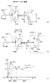
(1) 実施例1の発光サイリスタ210のターンオン過程の説明
図21−1(a)〜(c)は、本実施例1の図7に示す発光サイリスタ210のターンオン過程を示す動作説明図であり、同図(a)、(b)は図7の発光サイリスタ210(=210−1〜210−96)のゲートを駆動するための図14のバッファ163(=163−1〜163−96)の動作を説明する要部の回路図、及び、同図(c)は発光サイリスタ210のターンオン過程を示す動作波形図である。
(1) Description of Turn-On Process of Light-Emitting
図21−1(a)、(b)には、共通のバッファ162−1、個別のバッファ163−1、及び発光サイリスタ210−1の要部が抜き出され、更に、個別のバッファ163−1の内部構成及び発光サイリスタ210−1の等価回路も示されている。 21A and 21B, the main parts of the common buffer 162-1, the individual buffer 163-1, and the light-emitting thyristor 210-1 are extracted, and further, the individual buffers 163-1 are extracted. And the equivalent circuit of the light emitting thyristor 210-1.
図21−1(a)、(b)において、共通のバッファ63−1は、NPNTR401及び402により構成されている。発光サイリスタ210−1は、PNPTR221及びNPNTR222により構成されている。図21−1(a)、(b)中のVbe(=Vf)はNPNTR401,402のベース・エミッタ間電圧、IbはPNPTR221のベース電流、Igは発光サイリスタ210−1のゲート電流、Vgは発光サイリスタ210−1のゲート電圧、Vaは発光サイリスタ210−1のアノード電圧、Ikは発光サイリスタ210−1のカソード電流Ikである。
In FIGS. 21A and 21B, the common buffer 63-1 is composed of NPNTRs 401 and 402. The light emitting thyristor 210-1 is configured by a
例えば、図21−1(a)において、発光サイリスタ210−1のターンオン過程を説明するために、バッファ162−1の入力端子がLレベルになっているとする。発光サイリスタ210−1を駆動するために、図6のドライバIC100中のDO1端子からアノード電流Iaが出力される。この時、バッファ162−1の出力端子はLレベルとなる。発光サイリスタ210−1のアノードに注入されたアノード電流Iaは、PNPTR221のエミッタ・ベース間をベース電流Ibとして流れ、更に、発光サイリスタ210−1のゲート電流Igとしてバッファ163−1内のNPNTR402のベース・エミッタ間を流れて、バッファ162−1の出力端子に流れ込むことになる
For example, in FIG. 21A, it is assumed that the input terminal of the buffer 162-1 is at the L level in order to explain the turn-on process of the light emitting thyristor 210-1. In order to drive the light emitting thyristor 210-1, the anode current Ia is output from the DO1 terminal in the
バッファ162−1の出力端子はLレベルであり、この電位はグランド電位と略等しい0Vであるので、発光サイリスタ210−1のゲート電圧Vgは、NPNTR401,402のベース・エミッタ間電圧Vbeと略等しいものとなる。
Since the output terminal of the buffer 162-1 is at the L level and this potential is 0V which is substantially equal to the ground potential, the gate voltage Vg of the light emitting thyristor 210-1 is substantially equal to the base-emitter voltage Vbe of the
図21−1(b)において、発光サイリスタ210−1のゲート電流1gは、内部のPNPTR221のベース電流Ibに相当するものであり、このベース電流Ibが流れることで、PNPTR221がオン状態への移行を開始して、このPNPTR221のコレクタにはコレクタ電流を生じる。PNPTR221のコレクタ電流は、NPNTR222のベース電流となり、このNPNTR222をオン状態へと移行させる。PNPTR222のオン状態への移行により生じたコレクタ電流は、PNPTR221のベース電流Ibを増強し、このPNPTR221のオン状態への移行を加速させることになる。
In FIG. 21-1 (b), the gate current 1g of the light emitting thyristor 210-1 corresponds to the base current Ib of the
一方、NPNトTR222が完全にオン状態に移行した後には、そのコレクタ・エミッタ間電圧が低下して、NPNTR402のベース・エミッタ間電圧Vbeよりも小さい電圧となる。この結果、発光サイリスタ210−1のゲートからバッファ163−1の第2端子T2側に流れるゲート電流1gは略ゼロとなって、発光サイリスタ210−1のカソードには、アノード電流Iaと略等しいカソード電流Ikが流れることになり、発光サイリスタ210−1が完全にオン状態となる。 On the other hand, after the NPN transistor TR222 is completely turned on, the collector-emitter voltage decreases to a voltage smaller than the base-emitter voltage Vbe of the NPNTR402. As a result, the gate current 1g flowing from the gate of the light emitting thyristor 210-1 to the second terminal T2 side of the buffer 163-1 becomes substantially zero, and the cathode of the light emitting thyristor 210-1 has a cathode substantially equal to the anode current Ia. The current Ik flows, and the light emitting thyristor 210-1 is completely turned on.
図21−1(c)は、前記発光サイリスタ210−1のターンオン過程を説明する図で、あって、横軸にアノード電流1a、縦軸にアノード電圧Vaが示されている。 FIG. 21C is a diagram for explaining the turn-on process of the light-emitting thyristor 210-1. The horizontal axis represents the anode current 1a, and the vertical axis represents the anode voltage Va.
発光サイリスタ210−1の消灯状態においてはアノード電流Iaが略ゼロであり、図21−1(c)の原点(0,0)の状態にある。発光サイリスタ210−1のターンオン開始に伴い、アノード駆動が行われると、図21−1(c)中の矢印で示したように、アノード電圧Vaが上昇して最大電圧Vpに到達する。この最大電圧Vpは、NPNTR402のベース・エミッタ間電圧Vbeと、PNPTR221のベース・エミッタ間電圧Vbeとの加算値に対応するものであり、最大電圧Vpが順方向に印加されることで、ゲート電流Ig(=PNPTR221のベース電流Ib)を生じる。
In the light-off state of the light-emitting thyristor 210-1, the anode current Ia is substantially zero, and is in the state of the origin (0, 0) in FIG. 21-1 (c). When anode driving is performed with the start of turn-on of the light-emitting thyristor 210-1, the anode voltage Va rises and reaches the maximum voltage Vp, as indicated by the arrow in FIG. 21-1 (c). The maximum voltage Vp corresponds to the sum of the base-emitter voltage Vbe of the
図21−1(c)において、丸印を付して示すポイント(Ip,Vp)は、発光サイリスタ210−1のオフ領域AR1とオン遷移領域AR2の境目に相当している。次いで、アノード電流1aが増加するに伴い、アノード電圧Vaが低下していき、丸印を付して示すポイント(Iv,Vv)に到達する。このポイント(Iv,Vv)は、発光サイリスタ210−1のオン遷移領域AR2とオン領域AR3との境目に相当しており、この時のゲート電流Igは略ゼロにまで低下していて、実質的にバッファ163−1は発光サイリスタ210−1から切り離されたのと等価な状態にある。 In FIG. 21-1 (c), a point (Ip, Vp) indicated by a circle corresponds to the boundary between the off region AR1 and the on transition region AR2 of the light emitting thyristor 210-1. Next, as the anode current 1a increases, the anode voltage Va decreases and reaches a point (Iv, Vv) indicated by a circle. This point (Iv, Vv) corresponds to the boundary between the on-transition region AR2 and the on-region AR3 of the light emitting thyristor 210-1, and the gate current Ig at this time is substantially reduced to zero. In addition, the buffer 163-1 is equivalent to being disconnected from the light emitting thyristor 210-1.
更にアノード電流Iaが増加するに伴い、アノード電圧Vaが増加していき、丸印を付して示すポイント(Il,Vl)に到達する。このポイント(Il,Vl)は、発光サイリスタ210−1における発光駆動の最終動作ポイントであり、ドライバIC100側から供給されるアノード電流Iaに応じた所定の発光パワーで発光駆動が行われる。
As the anode current Ia further increases, the anode voltage Va increases, and reaches a point (Il, Vl) indicated by a circle. This point (Il, Vl) is the final operation point of light emission driving in the light emitting thyristor 210-1, and light emission driving is performed with a predetermined light emission power corresponding to the anode current Ia supplied from the
図21−1(c)を用いて発光サイリスタ210−1のターンオン過程を説明したが、個別のバッファ163−1を設けることで、オン状態にある発光サイリスタ210−1からのゲート電流Igの流れ込みを防止して、アノード電流Iaとカソード電流Ikを略等しくしたオン状態駆動とすることができて、アノード電流Iaを調整することでそれに応じた発光パワーを得ることができる。このような動作は、バッファ162−1の出力端子と発光サイリスタ210−1のゲートとの間に個別のバッファ163−1を介在させたことによる効果である。 Although the turn-on process of the light-emitting thyristor 210-1 has been described with reference to FIG. 21-1 (c), the gate current Ig flows from the light-emitting thyristor 210-1 in the on state by providing the individual buffer 163-1. , And an on-state drive in which the anode current Ia and the cathode current Ik are substantially equal to each other. By adjusting the anode current Ia, light emission power corresponding to the on-state drive can be obtained. Such an operation is an effect obtained by interposing an individual buffer 163-1 between the output terminal of the buffer 162-1 and the gate of the light emitting thyristor 210-1.
仮に、通常のCMOS回路で構成したバッファ162−1と発光サイリスタ210−1のゲートとを直結した場合には、バッファ162−1のLレベル出力電位は略0Vにまで降下してしまうので、PNPTR221のベース電流Ibがバッファ162−1の出力端子側にゲート電流Igとして流れ続け、その分NPNTR222のコレクタ電流Ikが減少して、発光サイリスタ210−1のカソード電流Ikも減少してしまう。この結果、発光サイリスタ210−1の発光出力が変動してしまって所望状態で動作させることができず、発光サイリスタ210を用いてプリントヘッド13を実現することが困難になるといった不具合が生じる。
If the buffer 162-1 configured with a normal CMOS circuit and the gate of the light-emitting thyristor 210-1 are directly connected, the L level output potential of the buffer 162-1 drops to approximately 0V, so the
これに対し、本実施例1によれば、ゲート駆動用の個別のバッファ163−1を設けているので、前記不具合が生じることが無くなり、印刷品位に優れた画像形成装置1を実現できる。
On the other hand, according to the first embodiment, since the individual buffer 163-1 for driving the gate is provided, the above-described problem does not occur and the
(2) 比較例の同時オンの場合の動作
図21−2(a)、(b)は、本実施例1に対する比較例を示す動作説明図である。
(2) Operation when the comparative example is turned on simultaneously FIGS. 21-2 (a) and (b) are operation explanatory views showing a comparative example with respect to the first embodiment.
この図21−2(a)においては、説明を簡略化するために、共通のバッファ162−1の出力端子には、2個の発光サイリスタ210−1,210−3のみが接続され、他の発光サイリスタの図示が省略されている。更に、図21−2(b)は、図21−1(a)と対比させて描かれており、各発光サイリスタ210−1,210−3の内部等価回路が、実施例1と同様に、PNPTR221及びNPNTR222により構成されている。
In FIG. 21-2 (a), in order to simplify the description, only two light-emitting thyristors 210-1 and 210-3 are connected to the output terminal of the common buffer 162-1. The illustration of the light emitting thyristor is omitted. Furthermore, FIG. 21-2 (b) is drawn in contrast with FIG. 21-1 (a), and the internal equivalent circuit of each light-emitting thyristor 210-1, 210-3 is similar to the first embodiment. The
図21−2(a)に示す比較例では、共通のバッファ162−1の出力端子が、共通配線GLを介して、複数の発光サイリスタ210−1,210−3,・・・のゲートに接続されている。このような比較例の構成において、複数の発光サイリスタ210−1,210−3,・・・が同時に点灯した場合の挙動を説明する。 In the comparative example shown in FIG. 21-2 (a), the output terminal of the common buffer 162-1 is connected to the gates of the plurality of light-emitting thyristors 210-1, 210-3,... Via the common wiring GL. Has been. In the structure of such a comparative example, the behavior when a plurality of light emitting thyristors 210-1, 210-3,.
図21−2(a)において、発光サイリスタ210−1,210−3の同時オンの状況を示すために、ゲート駆動用のバッファ162−1の入力レベルをLレベルとする。 In FIG. 21-2 (a), the input level of the gate driving buffer 162-1 is set to L level in order to show the simultaneous ON state of the light emitting thyristors 210-1 and 210-3.
図21−2(b)において、バッファ162−1の出力レベルをLレベルとさせて発光サイリスタ210−1,210−3をオンさせた後には、発光サイリスタ210−1,210−3のゲートからバッファ162−1の出力端子に向かって流れ込む電流を略ゼロとすることができるものと仮定して、共通配線GLに接続されるバッファ162−1が破線にて描かれている。 In FIG. 21B, after the light emitting thyristors 210-1 and 210-3 are turned on by setting the output level of the buffer 162-1 to the L level, the gates of the light emitting thyristors 210-1 and 210-3 are turned on. Assuming that the current flowing toward the output terminal of the buffer 162-1 can be made substantially zero, the buffer 162-1 connected to the common line GL is drawn with a broken line.
例えば、発光サイリスタ210−1がオンしており、このアノードからアノード電流Ia1が流入しているとする。この時、アノード電流Ia1は、I1,I2,I3の3つの電流成分の合計となる。即ち、電流I1は、図21−2において実線矢印で示すように、発光サイリスタ210−1のアノードからPNPTR221のエミッタ・コレクタ間を通り、NPNTR222のベース・エミッタ間を通してグランドGNDに至る電流である。電流I2は、破線矢印で示すように、アノードからPNPTR221のエミッタ・ベース間を通り、NPNTR222のコレクタ・エミッタ間を通してグランドGNDに至る電流である。更に、電流I3は、一点鎖線で示すように、アノードからPNPTR221のエミッタ・ベース間を通り、共通配線GLを介して他の発光サイリスタ210−3のゲートから流入して、この発光サイリスタ210−3内部のNPNTR222のコレクタ・エミッタ間を通してグランドGNDに至る電流である。
For example, it is assumed that the light emitting thyristor 210-1 is on and the anode current Ia1 flows from the anode. At this time, the anode current Ia1 is the sum of the three current components I1, I2, and I3. That is, the current I1 is a current from the anode of the light-emitting thyristor 210-1 through the emitter and collector of the
実施例1で設定される発光サイリスタ210−1,210−3においては、この発光は主としてPNPTR221に流れる電流によって生じる特性を備えており、前記電流I1〜I3毎の発光パワー(P)の成分(Pi1,Pi2,Pi3)への寄与の大きい順に表せば、
Pi1>Pi2>Pi3
となる。そのため、一点鎖線で示す電流I3が生じることにより、本来流すべき電流I1の成分が減少して、全体としての発光出力が減少してしまうことになる。このように、比較例の構成においては、同時に発光している発光サイリスタ210−1,210−3相互に共通配線GLを介して回り込み電流I3を生じる。この回り込み電流I3の大きさは、発光サイリスタ210−1,210−3等のゲート・カソード間電圧のばらつき、駆動状態、共通配線GLの微小な配線抵抗値等によって様々に変動してしまう。この結果、光量変動により、画像形成装置1における印刷濃度にむらを生じてしまい、印刷品位を著しく低下させていたのである。
In the light emitting thyristors 210-1 and 210-3 set in the first embodiment, this light emission has characteristics mainly caused by the current flowing through the
Pi1>Pi2> Pi3
It becomes. Therefore, when the current I3 indicated by the alternate long and short dash line is generated, the component of the current I1 that should be flown is reduced, and the light emission output as a whole is reduced. Thus, in the configuration of the comparative example, the sneak current I3 is generated between the light emitting thyristors 210-1 and 210-3 that emit light simultaneously through the common wiring GL. The magnitude of the sneak current I3 varies in various ways depending on variations in the gate-cathode voltages of the light emitting thyristors 210-1, 210-3, the driving state, a minute wiring resistance value of the common wiring GL, and the like. As a result, the variation in the amount of light causes unevenness in the print density in the
(3) 実施例1の同時オンの場合の動作
図21−3(a)、(b)は、本実施例1の図7に示す複数の発光サイリスタ210−1,210−3,・・・が同時に点灯した場合の挙動を示す動作説明図である。
(3) Operation when the first embodiment is turned on simultaneously FIGS. 21-3 (a) and 21 (b) show a plurality of light emitting thyristors 210-1, 210-3,... Shown in FIG. It is operation | movement explanatory drawing which shows the behavior at the time of turning on simultaneously.
この図21−3(a)においては、説明を簡略化するために、共通のバッファ162−1の出力端子に接続された共通配線GLには、2個の個別のバッファ163−1,163−3の第1端子T1が接続され、このバッファ163−1,163−3の第2端子T2に、2個の発光サイリスタ210−1,210−3が接続され、他のバッファ及び発光サイリスタの図示が省略されている。共通のバッファ162−1は、発光サイリスタ210−1,210−3,・・・のオン制御に伴いその入力レベルがLレベルとされるので、グランドGNDに接続して示している。 In FIG. 21-3 (a), in order to simplify the description, the common wiring GL connected to the output terminal of the common buffer 162-1 has two separate buffers 163-1 and 163-1. Three first terminals T1 are connected, and two light emitting thyristors 210-1 and 210-3 are connected to the second terminal T2 of the buffers 163-1 and 163-3, and other buffers and light emitting thyristors are shown. Is omitted. The common buffer 162-1 is shown connected to the ground GND because its input level is set to L level as the light emitting thyristors 210-1, 210-3,.
更に、図21−3(b)は、図21−3(a)と対比させて描かれており、各個別のバッファ163−1,163−3の内部等価回路が、NPNTR401,402により構成され、更に、各発光サイリスタ210−1,210−3の内部等価回路が、PNPTR221及びNPNTR222により構成されている。図21−3(b)中のVce1は、発光サイリスタ210−1内のNPNTR222のコレクタ・エミッタ間電圧であり、Vce3は、発光サイリスタ210−3内のNPNTR222のコレクタ・エミッタ間電圧である。
Furthermore, FIG. 21-3 (b) is drawn in contrast with FIG. 21-3 (a), and the internal equivalent circuits of the individual buffers 163-1 and 163-3 are configured by
なお、図21−3(b)は、複数の発光サイリスタ210−1,210−3が同時にオンしている状況を示しているが、図21−1と同様に、本実施例1の構成を用いた個別のバッファ163−1,163−3においては、発光サイリスタ210−1,210−3のターンオン指令のために、そのバッファ163−1,163−3の第2端子T2をLレベルにして発光サイリスタ210−1,210−3をオンさせた後には、この発光サイリスタ210−1,210−3のゲートから個別のバッファ163−1,163−3の第2端子T2に向かつて流れ込む電流を略ゼロにすることができる。このため、図21−3(b)においては、共通配線GLに接続される共通のバッファ162−1の影響は除外して考えることができ、図21−3(b)においてはバッファ162−1を破線にて図示している。 FIG. 21-3 (b) shows a situation in which a plurality of light-emitting thyristors 210-1 and 210-3 are turned on at the same time. As in FIG. In the individual buffers 163-1 and 163-3 used, the second terminals T2 of the buffers 163-1 and 163-3 are set to L level in order to turn on the light-emitting thyristors 210-1 and 210-3. After the light emitting thyristors 210-1 and 210-3 are turned on, a current flowing from the gates of the light emitting thyristors 210-1 and 210-3 toward the second terminals T2 of the individual buffers 163-1 and 163-3 is supplied. It can be almost zero. Therefore, in FIG. 21-3 (b), the influence of the common buffer 162-1 connected to the common wiring GL can be excluded, and in FIG. 21-3 (b), the buffer 162-1 can be considered. Is shown by a broken line.
例えば、発光サイリスタ210−1がオンしており、そのアノードからアノード電流Ia1が流入しているとする。この時、発光サイリスタ210−1におけるゲート電流Igの流れる経路として、図21−3(b)中の破線矢印で示す経路を考える。破線矢印のゲート電流Igが流れると仮定すると、このゲート電流Igは、発光サイリスタ210−1内のPNPTR221のエミッタ・ベース間を通り、個別のバッファ163−1中のNPNTR402のベース・エミッタ間を通り、ベース・エミッタ間電圧Vbe分だけ電位降下した後、共通配線GLを経由して、他の個別のバッファ163−3中のNPNTR401のベース・エミッタ間を通り、ベース・エミッタ間電圧Vbe分だけ電位降下して、発光サイリスタ210−3内のNPNTR222のコレクタ・エミッタ間を経由してグランドGNDに流出する。そのため、発光サイリスタ210−1のゲートからゲート電流Igの流出側に向かつて積算した電圧Vgは、
Vg=Vbe+Vbe+Vce3
となる。
For example, it is assumed that the light-emitting thyristor 210-1 is on and the anode current Ia1 flows from its anode. At this time, as a path through which the gate current Ig flows in the light emitting thyristor 210-1, a path indicated by a broken-line arrow in FIG. 21-3 (b) is considered. Assuming that a gate current Ig indicated by a broken arrow flows, this gate current Ig passes between the emitter and base of the
Vg = Vbe + Vbe + Vce3
It becomes.
ところが、発光サイリスタ210−1中のNPNTR222のコレクタ・エミッタ間電圧Vce1は、前記電圧Vgの計算値よりも小さいので、発光サイリスタ210−1内のPNPTR221のベースを流れたベース電流Ibは、破線矢印の経路を通ることなく、NPNTR222のコレクタ電流となって、発光サイリスタ210−1自身のカソード電流Ikとして合流することになる。
However, since the collector-emitter voltage Vce1 of the
図1及び図6から明らかなように、同時に点灯する発光サイリスタ210−1,210−3,・・・において、そのゲートには個別のバッファ163−1,163−3,・・・が配備されており、前記発光サイリスタ210−1,210−3のゲート間を流れる電流成分は発生しないことになる。この結果、発光サイリスタ210−1,210−3に供給するアノード電流Ia1,Ia3は、全てこの発光サイリスタ210−1,210−3のアノード・カソード間を流れてカソード電流Ikとなり、アノード電流Ia1,Ia3とカソード電流Ik,Ikは等しいので、発光サイリスタ210−1,210−3の発光出力は、アノード電流Ia1,Ia3のみにより変化させることができて、このアノード電流Ia1,Ia3を調整することによってその発光パワーを任意に調整することができる。 As apparent from FIGS. 1 and 6, in the light emitting thyristors 210-1, 210-3,... That are turned on at the same time, individual buffers 163-1, 163-3,. Thus, no current component flows between the gates of the light emitting thyristors 210-1 and 210-3. As a result, the anode currents Ia1 and Ia3 supplied to the light-emitting thyristors 210-1 and 210-3 all flow between the anode and cathode of the light-emitting thyristors 210-1 and 210-3 to become the cathode current Ik. Since Ia3 and the cathode currents Ik and Ik are equal, the light emission outputs of the light emitting thyristors 210-1 and 210-3 can be changed only by the anode currents Ia1 and Ia3, and the anode currents Ia1 and Ia3 are adjusted. The light emission power can be arbitrarily adjusted.
このように、本実施例1の構成においては、同時にオンしている発光サイリスタ210−1,210−3のゲート間には回りこみ電流を生じることはなく、そのアノード電流Ia1,Ia3により発光出力を調整することができる。 As described above, in the configuration of the first embodiment, no sneak current is generated between the gates of the light-emitting thyristors 210-1 and 210-3 that are turned on simultaneously, and the anode currents Ia1 and Ia3 emit light. Can be adjusted.
(実施例1の効果)
本実施例1によれば、次の(a)、(b)のような効果がある。
(Effect of Example 1)
According to the first embodiment, there are the following effects (a) and (b).
(a) 多数の発光サイリスタ210が配列され、これらが複数の組(例えば、偶数と奇数の組)に分けられ、各組の発光サイリスタ列が各組毎に時分割に駆動されるプリントヘッド13において、同一組に属する発光サイリスタ列における各発光サイリスタ210のゲートを、個別のバッファ(例えば、163)を介して共通配線GLにそれぞれ接続して共通に駆動する構成になっているので、同時点灯する発光サイリスタ(例えば、210−1,210−3,・・・)のゲート間に流れる回り込み電流を略ゼロにすることができる。これにより、回り込み電流が流れることで生じる発光出力の変動を未然に防止できる。
(A) A large number of light-emitting
(b) 発光出力の変動を防止できるので、プリントヘッド13に起因する印刷濃度むらを解消して、印刷品位に優れ、スペース効率及び光取り出し効率に優れた画像形成装置1を実現できる。即ち、プリントヘッド13を用いることにより、本実施例1のフルカラーの画像形成装置1に限らず、モノクロ、マルチカラーの画像形成装置においても効果が得られるが、特に、露光装置としてのプリントヘッド13を数多く必要とするフルカラーの画像形成装置1において一層大きな効果が得られる。
(B) Since fluctuations in the light emission output can be prevented, it is possible to eliminate the print density unevenness caused by the
本発明の実施例2において、図2の画像形成装置1、図6のプリントヘッド13、及び図1のドライバIC100の構成は、実施例1と同様であり、本実施例2の個別のバッファの構成のみが、実施例1における図1及び図14の個別のバッファ163,164と異なるので、その異なる点を以下説明する。
In the second embodiment of the present invention, the configurations of the
(実施例2の個別のバッファ)
図22(a)〜(d)は、本発明の実施例2における個別のバッファの構造を示す模式図であり、同図(a)は回路シンボルを示す図、同図(b)は同図(a)の回路構成を示す図、同図(c)は同図(b)の回路をICとして実現したときの概略の断面構造を示す図、及び、同図(d)は同図(b)、(c)の電圧/電流特性を示す図である。この図22において、実施例1を示す図14中の要素と共通の要素には共通の符号が付されている。
(Individual buffer of Example 2)
FIGS. 22A to 22D are schematic views showing the structure of individual buffers according to the second embodiment of the present invention. FIG. 22A is a diagram showing circuit symbols, and FIG. The figure which shows the circuit structure of (a), the figure (c) is a figure which shows schematic sectional structure when the circuit of the figure (b) is implement | achieved as IC, and the figure (d) is the figure (b). It is a figure which shows the voltage / current characteristic of (c). In FIG. 22, elements common to those in FIG. 14 showing the first embodiment are denoted by common reference numerals.
図22(a)に示すように、本実施例2における分離回路としての個別のバッファ163Aは、入力側の第1端子T1及び出力側の第2端子T2を有している。
As shown in FIG. 22A, the
なお、実施例1のバッファ164は、バッファ163と同一の回路構成であり、この実施例1のバッファ164に対応する本実施例3のバッファは、バッファ163Aと同一の回路構成であるので、以下、バッファ163Aについてのみ説明する。
The
図22(b)に示すように、個別のバッファ163Aは、第1トランジスタ(例えば、NPNTR)421及び第2トランジスタ(例えば、PNPTR)422を有し、これらが入力側の第1端子T1と出力側の第2端子T2との間に接続されて、バッファ回路が構成されている。即ち、NPNTR421のベースとPNPTR422のベースとは、第1端子T1に接続され、NPNTR421のコレクタが電源電圧VDD端子に接続されている。NPNTR421のエミッタは、第2端子T2及びPNPTR422のエミッタに接続され、このPNPTR422のコレクタがグランドGNDに接続されている。
As shown in FIG. 22B, the
図22(c)に示すように、IC等が形成されているP型不純物を含んだP型基材410上の所定箇所には、N型不純物を注入してNウェル領域411が形成されている。Nウェル領域411内には、P型不純物を拡散させてP型領域414が形成されている。
As shown in FIG. 22C, an
なお、図22(c)においては図面を簡略化するために、ゲート酸化膜、コンタクトホール、保護膜であるパッシベーション膜等の図示を省略している。図示しない金属配線により、P型領域414がエミッタEに、Nウェル領域411がベースBに、P型基材410がコレクタCにそれぞれ接続され、PNPTR422が構成されている。NPNTR421の断面構造は、実施例1のNPNTR401,402の断面構造を示す図14(c)と同様である。
Note that in FIG. 22C, illustration of a gate oxide film, a contact hole, a passivation film as a protective film, and the like is omitted for the sake of simplicity. A P-
図22(d)に示すバッファ163Aの電圧/電流特性図において、横軸は図22 (b)の第1端子T1と第2端子T2間に印加される電圧(V)、縦軸は第1端子T1と第2端子T2間に流れる電流(I)を示している。この特性図から明らかなように、第1端子T1と第2端子T2間に印加される電圧Vの絶対値が電圧Vfを越えると、電流Iが流れる特性となっている。その電圧Vfは、NPNTR421及びPNPTR422のベース・エミッタ間の順電圧(即ち、ベース・エミッタ間電圧Vbe)に等しく、図22(c)のバッファ163Aをシリコン基材を用いて形成した場合における電圧Vfの典型例は、約0.6Vである。
In the voltage / current characteristic diagram of the
(発光サイリスタの動作)
本実施例2における発光サイリスタ210(=210−1〜210−96)及びバッファ162−1,163A(=163A−1〜163A−96)の動作(1)、(2)を、以下説明する。
(Operation of light-emitting thyristor)
Operations (1) and (2) of the light-emitting thyristor 210 (= 210-1 to 210-96) and the buffers 162-1 and 163A (= 163A-1 to 163A-96) in the second embodiment will be described below.
なお、バッファ163A(=163A−1〜163A−96)は、実施例1の図1に示すバッファ163(=163−1〜163−96)に対応している。
The
(1) 実施例2の発光サイリスタ210のターンオン過程の説明
図23−1(a)〜(c)は、本実施例2の図7に示す発光サイリスタ210のターンオン過程を示す動作説明図であり、実施例1の図21−1(a)〜(c)に対応している。図23−1(a)、(b)は、図7の発光サイリスタ210(=210−1〜210−96)のゲートを駆動するための図22のバッファ163A(=163A−1〜163A−96)の動作を説明する要部の回路図、及び、図23−1(c)は、発光サイリスタ210のターンオン過程を示す動作波形図である。
(1) Description of Turn-On Process of Light-Emitting
図23−1(a)、(b)には、共通のバッファ162−1、個別のバッファ163A−1、及び発光サイリスタ210−1の要部が抜き出され、更に、個別のバッファ163A−1の内部構成及び発光サイリスタ210−1の等価回路も示されている。
In FIGS. 23A and 23B, the main parts of the common buffer 162-1, the
図23−1(a)、(b)において、共通のバッファ63−1は、実施例1と同様に、NPNTR401及び402により構成されている。発光サイリスタ210−1は、PNPTR221及びNPNTR222により構成されている。図23−1(a)、(b)中のVbe(=Vf)はNPNTR421及びPNPTR422のベース・エミッタ間電圧、IbはPNPTR221のベース電流、Igは発光サイリスタ210−1のゲート電流、Vgは発光サイリスタ210−1のゲート電圧、Vaは発光サイリスタ210−1のアノード電圧、Ikは発光サイリスタ210−1のカソード電流Ikである。
In FIGS. 23A and 23B, the common buffer 63-1 is configured by
例えば、図23−1(a)において、発光サイリスタ210−1のターンオン過程を説明するために、バッファ162−1の入力端子がLレベルになっているとする。発光サイリスタ210−1を駆動するために、図6のドライバIC100中のDO1端子からアノード電流Iaが出力される。この時、バッファ162−1の出力端子はLレベルとなる。発光サイリスタ210−1のアノードに注入されたアノード電流Iaは、PNPTR221のエミッタ・ベース間をベース電流Ibとして流れ、更に、発光サイリスタ210−1のゲート電流Igとしてバッファ163A−1内のPNPTR422のベース・エミッタ間を流れて、バッファ162−1の出力端子に流れ込むことになる
For example, in FIG. 23A, in order to explain the turn-on process of the light emitting thyristor 210-1, it is assumed that the input terminal of the buffer 162-1 is at the L level. In order to drive the light emitting thyristor 210-1, the anode current Ia is output from the DO1 terminal in the
バッファ162−1の出力端子はLレベルであり、この電位はグランド電位と略等しい0Vであるので、発光サイリスタ210−1のゲート電圧Vgは、NPNTR421及びPNPTR422のベース・エミッタ間電圧Vbe(=Vf)と略等しいものとなる。
Since the output terminal of the buffer 162-1 is at the L level and this potential is 0 V which is substantially equal to the ground potential, the gate voltage Vg of the light emitting thyristor 210-1 is the base-emitter voltage Vbe (= Vf) of the
図23−1(b)において、発光サイリスタ210−1のゲート電流1gは、内部のPNPTR221のベース電流Ibに相当するものであり、このベース電流Ibが流れることで、PNPTR221がオン状態への移行を開始して、このPNPTR221のコレクタにはコレクタ電流を生じる。PNPTR221のコレクタ電流は、NPNTR222のベース電流となり、このNPNTR222をオン状態へと移行させる。PNPTR222のオン状態への移行により生じたコレクタ電流は、PNPTR221のベース電流Ibを増強し、このPNPTR221のオン状態への移行を加速させることになる。
In FIG. 23-1 (b), the gate current 1g of the light emitting thyristor 210-1 corresponds to the base current Ib of the
一方、NPNTR222が完全にオン状態に移行した後には、そのコレクタ・エミッタ間電圧が低下して、PNPTR422のベース・エミッタ間電圧Vbeよりも小さい電圧となる。この結果、発光サイリスタ210−1のゲートからバッファ163A−1の第2端子T2側に流れるゲート電流1gは略ゼロとなって、発光サイリスタ210−1のカソードには、アノード電流Iaと略等しいカソード電流Ikが流れることになり、発光サイリスタ210−1が完全にオン状態となる。
On the other hand, after
図23−1(c)は、前記発光サイリスタ210−1のターンオン過程を説明する図で、あって、横軸にアノード電流1a、縦軸にアノード電圧Vaが示されている。 FIG. 23-1 (c) is a diagram for explaining the turn-on process of the light emitting thyristor 210-1. The horizontal axis indicates the anode current 1a, and the vertical axis indicates the anode voltage Va.
発光サイリスタ210−1の消灯状態においてはアノード電流Iaが略ゼロであり、図23−1(c)の原点(0,0)の状態にある。発光サイリスタ210−1のターンオン開始に伴い、アノード駆動が行われると、図23−1(c)中の矢印で示したように、アノード電圧Vaが上昇して最大電圧Vpに到達する。この最大電圧Vpは、PNPTR422のベース・エミッタ間電圧Vbeと、PNPTR221のベース・エミッタ間電圧Vbeとの加算値に対応するものであり、最大電圧Vpが順方向に印加されることで、ゲート電流Ig(=PNPTR221のベース電流Ib)を生じる。
In the light-off state of the light emitting thyristor 210-1, the anode current Ia is substantially zero, and is in the state of the origin (0, 0) in FIG. 23-1 (c). When the anode driving is performed with the start of turn-on of the light-emitting thyristor 210-1, the anode voltage Va rises and reaches the maximum voltage Vp as shown by the arrow in FIG. 23-1 (c). This maximum voltage Vp corresponds to the added value of the base-emitter voltage Vbe of the
図23−1(c)において、丸印を付して示すポイント(Ip,Vp)は、発光サイリスタ210−1のオフ領域AR1とオン遷移領域AR2の境目に相当している。次いで、アノード電流1aが増加するに伴い、アノード電圧Vaが低下していき、丸印を付して示すポイント(Iv,Vv)に到達する。このポイント(Iv,Vv)は、発光サイリスタ210−1のオン遷移領域AR2とオン領域AR3との境目に相当しており、この時のゲート電流Igは略ゼロにまで低下していて、実質的にバッファ163A−1は発光サイリスタ210−1から切り離されたのと等価な状態にある。
In FIG. 23-1 (c), a point (Ip, Vp) indicated by a circle corresponds to the boundary between the off region AR1 and the on transition region AR2 of the light emitting thyristor 210-1. Next, as the anode current 1a increases, the anode voltage Va decreases and reaches a point (Iv, Vv) indicated by a circle. This point (Iv, Vv) corresponds to the boundary between the on-transition region AR2 and the on-region AR3 of the light emitting thyristor 210-1, and the gate current Ig at this time is substantially reduced to zero. In addition, the
更にアノード電流Iaが増加するに伴い、アノード電圧Vaが増加していき、丸印を付して示すポイント(Il,Vl)に到達する。このポイント(Il,Vl)は、発光サイリスタ210−1における発光駆動の最終動作ポイントであり、ドライバIC100側から供給されるアノード電流Iaに応じた所定の発光パワーで発光駆動が行われる。
As the anode current Ia further increases, the anode voltage Va increases, and reaches a point (Il, Vl) indicated by a circle. This point (Il, Vl) is the final operation point of light emission driving in the light emitting thyristor 210-1, and light emission driving is performed with a predetermined light emission power corresponding to the anode current Ia supplied from the
図23−1(c)を用いて発光サイリスタ210−1のターンオン過程を説明したが、個別のバッファ163A−1を設けることで、オン状態にある発光サイリスタ210−1からのゲート電流Igの流れ込みを防止して、アノード電流Iaとカソード電流Ikを略等しくしたオン状態駆動とすることができて、アノード電流Iaを調整することでそれに応じた発光パワーを得ることができる。このような動作は、バッファ162−1の出力端子と発光サイリスタ210−1のゲートとの間に個別のバッファ163A−1を介在させたことによる効果である。
Although the turn-on process of the light-emitting thyristor 210-1 has been described with reference to FIG. 23-1 (c), the gate current Ig flows from the light-emitting thyristor 210-1 in the on state by providing the
実施例1において説明したように、仮に、通常のCMOS回路で構成したバッファ162−1と発光サイリスタ210−1のゲートとを直結した場合には、バッファ162−1のLレベル出力電位は略0Vにまで降下してしまうので、PNPTR221のベース電流Ibがバッファ162−1の出力端子側にゲート電流Igとして流れ続け、その分NPNTR222のコレクタ電流Ikが減少して、発光サイリスタ210−1のカソード電流Ikも減少してしまう。この結果、発光サイリスタ210−1の発光出力が変動してしまって所望状態で動作させることができず、発光サイリスタ210を用いてプリントヘッド13を実現することが困難になるといった不具合が生じる。
As described in the first embodiment, if the buffer 162-1 configured with a normal CMOS circuit and the gate of the light emitting thyristor 210-1 are directly connected, the L level output potential of the buffer 162-1 is approximately 0V. Therefore, the base current Ib of the
これに対し、本実施例2によれば、ゲート駆動用の個別のバッファ163A−1を設けているので、前記不具合が生じることが無くなり、印刷品位に優れた画像形成装置1を実現できる。
On the other hand, according to the second embodiment, since the
(2) 実施例2の同時オンの場合の動作
図23−2(a)、(b)は、本実施例2の図7に示す複数の発光サイリスタ210−1,210−3,・・・が同時に点灯した場合の挙動を示す動作説明図であり、実施例1の図21−3(a)、(b)に対応している。
(2) Operation when the second embodiment is turned on simultaneously FIGS. 23-2 (a) and 23 (b) show a plurality of light-emitting thyristors 210-1, 210-3,... Shown in FIG. FIG. 2 is an operation explanatory diagram showing the behavior when are simultaneously turned on, and corresponds to FIGS. 21-3 (a) and (b) of the first embodiment.
この図23−2(a)においては、説明を簡略化するために、共通のバッファ162−1の出力端子に接続された共通配線GLには、2個の個別のバッファ163A−1,163A−3(実施例1のバッファ163−1,163−3に対応)の第1端子T1が接続され、このバッファ163A−1,163A−3の第2端子T2に、2個の発光サイリスタ210−1,210−3が接続され、他のバッファ及び発光サイリスタの図示が省略されている。共通のバッファ162−1は、発光サイリスタ210−1,210−3,・・・のオン制御に伴いその入力レベルがLレベルとされるので、グランドGNDに接続して示している。
In FIG. 23-2 (a), in order to simplify the description, the common wiring GL connected to the output terminal of the common buffer 162-1 has two
更に、図23−2(b)は、図23−2(a)と対比させて描かれており、各個別のバッファ163A−1,163A−3の内部等価回路が、NPNTR421及びPNPTR422により構成され、更に、各発光サイリスタ210−1,210−3の内部等価回路が、PNPTR221及びNPNTR222により構成されている。図23−2(b)中のVce1は、発光サイリスタ210−1内のNPNTR222のコレクタ・エミッタ間電圧であり、Vce3は、発光サイリスタ210−3内のNPNTR222のコレクタ・エミッタ間電圧である。
Further, FIG. 23-2 (b) is drawn in contrast with FIG. 23-2 (a), and the internal equivalent circuit of each
なお、図23−2(b)は、複数の発光サイリスタ210−1,210−3が同時にオンしている状況を示しているが、図23−1と同様に、本実施例2の構成を用いた個別のバッファ163A−1,163A−3においては、発光サイリスタ210−1,210−3のターンオン指令のために、そのバッファ163A−1,163A−3の第2端子T2をLレベルにして発光サイリスタ210−1,210−3をオンさせた後には、この発光サイリスタ210−1,210−3のゲートから個別のバッファ163A−1,163A−3の第2端子T2に向かつて流れ込む電流を略ゼロにすることができる。このため、図23−2(b)においては、共通配線GLに接続される共通のバッファ162−1の影響は除外して考えることができ、図23−2(b)においてはバッファ162−1を破線にて図示している。
FIG. 23-2 (b) shows a situation in which a plurality of light-emitting thyristors 210-1 and 210-3 are simultaneously turned on, but the configuration of the second embodiment is similar to FIG. 23-1. In the
例えば、発光サイリスタ210−1がオンしており、そのアノードからアノード電流Ia1が流入しているとする。この時、発光サイリスタ210−1におけるゲート電流Igの流れる経路として、図23−2(b)中の破線矢印で示す経路を考える。破線矢印のゲート電流Igが流れると仮定すると、このゲート電流Igは、発光サイリスタ210−1内のPNPTR221のエミッタ・ベース間を通り、個別のバッファ163A−1中のPNPTR422のベース・エミッタ間を通り、ベース・エミッタ間電圧Vbe分だけ電位降下した後、共通配線GLを経由して、他の個別のバッファ163A−3中のNPNTR421のベース・エミッタ間を通り、ベース・エミッタ間電圧Vbe分だけ電位降下して、発光サイリスタ210−3内のNPNTR222のコレクタ・エミッタ間を経由してグランドGNDに流出する。そのため、実施例1と同様に、発光サイリスタ210−1のゲートからゲート電流Igの流出側に向かつて積算した電圧Vgは、
Vg=Vbe+Vbe+Vce3
となる。
For example, it is assumed that the light-emitting thyristor 210-1 is on and the anode current Ia1 flows from its anode. At this time, as a path through which the gate current Ig flows in the light emitting thyristor 210-1, a path indicated by a broken line arrow in FIG. Assuming that a gate current Ig indicated by a broken arrow flows, this gate current Ig passes between the emitter and base of the
Vg = Vbe + Vbe + Vce3
It becomes.
ところが、発光サイリスタ210−1中のNPNTR222のコレクタ・エミッタ間電圧Vce1は、前記電圧Vgの計算値よりも小さいので、発光サイリスタ210−1内のPNPTR221のベースを流れたベース電流Ibは、破線矢印の経路を通ることなく、NPNTR222のコレクタ電流となって、発光サイリスタ210−1自身のカソード電流Ikとして合流することになる。
However, since the collector-emitter voltage Vce1 of the
図1及び図6から明らかなように、同時に点灯する発光サイリスタ210−1,210−3,・・・において、そのゲートには個別のバッファ163A−1,163A−3,・・・(実施例1のバッファ163−1,163−3,・・・に対応)が配備されており、前記発光サイリスタ210−1,210−3のゲート間を流れる電流成分は発生しないことになる。この結果、発光サイリスタ210−1,210−3に供給するアノード電流Ia1,Ia3は、全てこの発光サイリスタ210−1,210−3のアノード・カソード間を流れてカソード電流Ikとなり、アノード電流Ia1,Ia3とカソード電流Ik,Ikは等しいので、発光サイリスタ210−1,210−3の発光出力は、アノード電流Ia1,Ia3のみにより変化させることができて、このアノード電流Ia1,Ia3を調整することによってその発光パワーを任意に調整することができる。
As is apparent from FIGS. 1 and 6, in the light emitting thyristors 210-1, 210-3,... That are turned on at the same time,
このように、本実施例2の構成においては、実施例1と同様に、同時にオンしている発光サイリスタ210−1,210−3のゲート間には回りこみ電流を生じることはなく、そのアノード電流Ia1,Ia3により発光出力を調整することができる。 Thus, in the configuration of the second embodiment, as in the first embodiment, no sneak current is generated between the gates of the light-emitting thyristors 210-1 and 210-3 that are turned on at the same time. The light emission output can be adjusted by the currents Ia1 and Ia3.
(実施例2の効果)
本実施例2によれば、各発光サイリスタ210のゲート側に、実施例1の個別のバッファ163又は164とは異なる回路構成の個別のバッファ163A又は164Aをそれぞれ接続したので、実施例1の効果(a)、(b)と同様の効果が得られる。
(Effect of Example 2)
According to the second embodiment, the
(実施例2の個別のバッファの変形例1)
図24(a)〜(c)は、本発明の実施例2における分離回路としての個別のバッファの変形例1を示す模式図であり、同図(a)は回路シンボルを示す図、同図(b)は同図(a)の回路構成を示す図、同図(c)は同図(b)の電圧/電流特性を示す図である。この図24において、実施例2を示す図22中の要素と共通の要素には共通の符号が付されている。
(
FIGS. 24A to 24C are schematic views showing Modification Example 1 of individual buffers as separation circuits in
図24(a)に示すように、本変形例1における個別のバッファ163Bは、入力側の第1端子T1及び出力側の第2端子T2を有している。
As shown in FIG. 24A, the
図24(b)に示すように、個別のバッファ163Bは、2つのPNPTR431,432を有し、これらが入力側の第1端子T1と出力側の第2端子T2との間に接続されて、バッファ回路が構成されている。即ち、PNPTR431のエミッタとPNPTR432のベースとは、第1端子T1に接続され、PNPTR431,432のコレクタが、グランドGNDに接続され、更に、PNPTR431のベースとPNPTR432のエミッタとが、第2端子T2に接続されている。
As shown in FIG. 24B, the
図24(c)に示すバッファ163Bの電圧/電流特性図において、横軸は図24 (b)の第1端子T1と第2端子T2間に印加される電圧(V)、縦軸は第1端子T1と第2端子T2間に流れる電流(I)を示している。この特性図から明らかなように、第1端子T1と第2端子T2間に印加される電圧Vの絶対値が電圧Vfを越えると、電流Iが流れる特性となっている。その電圧Vfは、PNPTR431,432のベース・エミッタ間の順電圧(即ち、ベース・エミッタ間電圧Vbe)に等しく、図24(b)のバッファ163Bをシリコン基材を用いて形成した場合における電圧Vfの典型例は、約0.6Vである。
In the voltage / current characteristic diagram of the
このような個別のバッファ163Bを各発光サイリスタ210のゲート側に接続しても、実施例2と同様の作用効果を奏することができる。
Even if such an
(実施例2の個別のバッファの変形例2)
図25(a)〜(c)は、本発明の実施例2における個別のバッファの変形例2を示す模式図であり、同図(a)は回路シンボルを示す図、同図(b)は同図(a)の回路構成を示す図、同図(c)は同図(b)の電圧/電流特性を示す図である。この図25において、実施例2を示す図22中の要素と共通の要素には共通の符号が付されている。
(
FIGS. 25A to 25C are schematic diagrams showing a second modification of the individual buffers according to the second embodiment of the present invention. FIG. 25A is a diagram showing circuit symbols, and FIG. The figure which shows the circuit structure of the figure (a), the figure (c) is a figure which shows the voltage / current characteristic of the figure (b). In FIG. 25, elements common to the elements in FIG. 22 illustrating the second embodiment are denoted by common reference numerals.
図25(a)に示すように、本変形例2における個別のバッファ163Cは、入力側の第1端子T1及び出力側の第2端子T2を有している。
As shown in FIG. 25A, the
図25(b)に示すように、個別のバッファ163Cは、2つのNPNTR441,442を有し、これらが入力側の第1端子T1と出力側の第2端子T2との間に接続されて、バッファ回路が構成されている。即ち、NPNTR441のベースとNPNTR442のエミッタとは、第1端子T1に接続され、NPNTR441,442のコレクタが、電源電圧VDD端子に接続され、更に、NPNTR441のエミッタとNPNTR442のベースとが、第2端子T2に接続されている。
As shown in FIG. 25B, the
図25(c)に示すバッファ163Cの電圧/電流特性図において、横軸は図25 (b)の第1端子T1と第2端子T2間に印加される電圧(V)、縦軸は第1端子T1と第2端子T2間に流れる電流(I)を示している。この特性図から明らかなように、第1端子T1と第2端子T2間に印加される電圧Vの絶対値が電圧Vfを越えると、電流Iが流れる特性となっている。その電圧Vfは、NPNTR441,442のベース・エミッタ間の順電圧(即ち、ベース・エミッタ間電圧Vbe)に等しく、図25(b)のバッファ163Cをシリコン基材を用いて形成した場合における電圧Vfの典型例は、約0.6Vである。
In the voltage / current characteristic diagram of the
このような個別のバッファ163Cを各発光サイリスタ210のゲート側に接続しても、実施例2と同様の作用効果を奏することができる。
Even if such an
(実施例2の個別のバッファの変形例3)
図26(a)〜(c)は、本発明の実施例2における個別のバッファの変形例3を示す模式図であり、同図(a)は回路シンボルを示す図、同図(b)は同図(a)の回路構成を示す図、同図(c)は同図(b)の電圧/電流特性を示す図である。この図26において、実施例2を示す図22中の要素と共通の要素には共通の符号が付されている。
(
FIGS. 26A to 26C are schematic views showing a third modification example of the individual buffer according to the second embodiment of the present invention. FIG. 26A is a diagram showing circuit symbols, and FIG. The figure which shows the circuit structure of the figure (a), the figure (c) is a figure which shows the voltage / current characteristic of the figure (b). In FIG. 26, elements common to the elements in FIG. 22 showing the second embodiment are denoted by common reference numerals.
図26(a)に示すように、本変形例3における個別のバッファ163Dは、入力側の第1端子T1及び出力側の第2端子T2を有している。
As shown in FIG. 26A, the
図26(b)に示すように、個別のバッファ163Dは、PNPTR451及びNPNTR452を有し、これらが入力側の第1端子T1と出力側の第2端子T2との間に接続されて、バッファ回路が構成されている。即ち、PNPTR451のエミッタとNPNTR452のエミッタとは、第1端子T1に接続され、PNPTR451のコレクタが、グランドGNDに接続され、NPNTR452のコレクタが、電源電圧VDD端子に接続され、更に、PNPTR451のベースとNPNTR452のベースとが、第2端子T2に接続されている。
As shown in FIG. 26 (b), the
図26(c)に示すバッファ163Dの電圧/電流特性図において、横軸は図26 (b)の第1端子T1と第2端子T2間に印加される電圧(V)、縦軸は第1端子T1と第2端子T2間に流れる電流(I)を示している。この特性図から明らかなように、第1端子T1と第2端子T2間に印加される電圧Vの絶対値が電圧Vfを越えると、電流Iが流れる特性となっている。その電圧Vfは、PNPTR451及びNPNTR452のベース・エミッタ間の順電圧(即ち、ベース・エミッタ間電圧Vbe)に等しく、図26(b)のバッファ163Dをシリコン基材を用いて形成した場合における電圧Vfの典型例は、約0.6Vである。
In the voltage / current characteristic diagram of the
このような個別のバッファ163Dを各発光サイリスタ210のゲート側に接続しても、実施例2と同様の作用効果を奏することができる。
Even when such an
(実施例1、2の他の変形例)
本発明は、上記実施例1、2や変形例1、2、3に限定されず、その他の利用形態や変形が可能である。この利用形態や変形例としては、例えば、次の(a)〜(c)のようなものがある。
(Other variations of Examples 1 and 2)
The present invention is not limited to the first and second embodiments and the first, second, and third embodiments, and can be used in other forms and modifications. For example, the following forms (a) to (c) are available as usage forms and modifications.
(a) 実施例において、光源として用いられる発光サイリスタ210に適用した場合について説明したが、本発明は、サイリスタをスイッチング素子として用い、このスイッチング素子に例えば直列に接続された他の素子(例えば、有機エレクトロルミネセンス素子(以下「有機EL素子」という。)、表示素子等)への電圧印加制御を行う場合にも適用可能である。例えば、有機EL素子のアレイで構成される有機ELプリントヘッドを備えたプリンタ、表示素子の列を有する表示装置等において利用することができる。
(A) In the embodiment, the case where the present invention is applied to the light-emitting
(b) 表示素子(例えば、列状あるいはマトリクス状に配列された表示素子)の駆動(即ち、電圧印加の制御)のためスイッチング素子としても用いられるサイリスタにも適用可能である。又、本発明は、3端子構造を備えたサイリスタの他、第1と第2の2つのゲート端子を備えた4端子サイリスタSCS(Silicon Semiconductor Controlled Switch)の場合にも適用可能である。 (B) The present invention can also be applied to a thyristor used as a switching element for driving (that is, controlling voltage application) of display elements (for example, display elements arranged in a column or matrix). The present invention can also be applied to a four-terminal thyristor SCS (Silicon Semiconductor Controlled Switch) having first and second gate terminals in addition to a thyristor having a three-terminal structure.
(c) 実施例1、2における発光サイリスタ210としてPNPN構造からなるNゲート型のものを取り上げてその構成及び動作を説明したが、Pゲート型サイリスタの構成においても同様な構成で動作させることができるのはもちろん、PNPNPN構成のサイリスタであっても良く、その形態は種々の変形が可能である。
(C) Although the configuration and operation of the
1 画像形成装置
13 プリントヘッド
100,100−1,100−2 ドライバIC
162−1,162−2 共通のバッファ
163,163A,163B,163C,163D,163−1〜163−96,163A−1,163A−3,164,164−1〜164−96 個別のバッファ
180 ドライバ部
181,181−1〜181−96 ドライバ
200,200−1,200−2 発光素子アレイ
210,210−1〜210−192 発光サイリスタ
401,402,421,441,442,452 NPNTR
422,431,432,451 PNPTR
DESCRIPTION OF
162-1, 162-2
422, 431, 432, 451 PNPTR
Claims (9)
前記各3端子発光素子の前記第2端子に対して前記駆動電流をそれぞれ供給する複数の駆動回路と、
前記各組における前記複数の3端子発光素子の前記制御端子を共通接続する共通配線と、
各々、前記共通配線に接続される第3端子と前記各3端子発光素子の前記制御端子に接続される第4端子とを有し、前記第3端子又は前記第4端子にそれぞれ入力される信号のレベルをシフトして前記第4端子又は前記第3端子からそれぞれ出力する複数の分離回路と、
を有することを特徴とする駆動装置。 A first terminal connected to a power source; a second terminal for passing a drive current between the first terminal; a control terminal for controlling a conduction state between the first terminal and the second terminal; The plurality of three-terminal light emitting elements having the first terminals connected in common are divided into a plurality of groups, and the plurality of three-terminal light emitting elements in each group are driven in a time-sharing manner for each group A driving device for
A plurality of drive circuits that respectively supply the drive current to the second terminals of the three-terminal light-emitting elements;
Common wiring for commonly connecting the control terminals of the plurality of three-terminal light emitting elements in each set;
Each of the signals has a third terminal connected to the common wiring and a fourth terminal connected to the control terminal of each of the three-terminal light emitting elements, and is input to the third terminal or the fourth terminal, respectively. A plurality of separation circuits that shift the output level and output from the fourth terminal or the third terminal, respectively,
A drive device comprising:
ダイオード接続された第1トランジスタとダイオード接続された第2トランジスタとを有し、前記第1トランジスタ及び前記第2トランジスタが前記第3端子と前記第4端子との間に逆並列状態に接続されていることを特徴とする請求項3記載の駆動装置。 The separation circuit is
A diode-connected first transistor and a diode-connected second transistor, wherein the first transistor and the second transistor are connected in antiparallel between the third terminal and the fourth terminal; The drive device according to claim 3, wherein
第1トランジスタ及び第2トランジスタを有し、前記第1トランジスタ及び前記第2トランジスタが前記第3端子と前記第4端子との間に接続されたバッファ回路により構成されていることを特徴とする請求項3記載の駆動装置。 The separation circuit is
A first transistor and a second transistor are provided, and the first transistor and the second transistor are configured by a buffer circuit connected between the third terminal and the fourth terminal. Item 4. The driving device according to Item 3.
請求項1〜7のいずれか1項に記載の駆動装置と、
を備えたことを特徴とするプリントヘッド。 A plurality of the three-terminal light emitting elements;
The drive device according to any one of claims 1 to 7,
A print head comprising:
前記プリントヘッドにより露光されて記録媒体に画像を形成することを特徴とする画像形成装置。 A print head according to claim 8,
An image forming apparatus which forms an image on a recording medium by being exposed by the print head.
Priority Applications (3)
| Application Number | Priority Date | Filing Date | Title |
|---|---|---|---|
| JP2010100208A JP2011233590A (en) | 2010-04-23 | 2010-04-23 | Driver, print head and image forming apparatus |
| EP11163147.9A EP2381320B1 (en) | 2010-04-23 | 2011-04-20 | Driver circuit, print head, and image forming apparatus |
| US13/064,876 US20110262184A1 (en) | 2010-04-23 | 2011-04-22 | Driver circuit, print head, and image forming apparatus |
Applications Claiming Priority (1)
| Application Number | Priority Date | Filing Date | Title |
|---|---|---|---|
| JP2010100208A JP2011233590A (en) | 2010-04-23 | 2010-04-23 | Driver, print head and image forming apparatus |
Publications (2)
| Publication Number | Publication Date |
|---|---|
| JP2011233590A true JP2011233590A (en) | 2011-11-17 |
| JP2011233590A5 JP2011233590A5 (en) | 2012-05-10 |
Family
ID=43911595
Family Applications (1)
| Application Number | Title | Priority Date | Filing Date |
|---|---|---|---|
| JP2010100208A Pending JP2011233590A (en) | 2010-04-23 | 2010-04-23 | Driver, print head and image forming apparatus |
Country Status (3)
| Country | Link |
|---|---|
| US (1) | US20110262184A1 (en) |
| EP (1) | EP2381320B1 (en) |
| JP (1) | JP2011233590A (en) |
Cited By (1)
| Publication number | Priority date | Publication date | Assignee | Title |
|---|---|---|---|---|
| CN110450541A (en) * | 2018-11-30 | 2019-11-15 | 虹光精密工业(苏州)有限公司 | Shift circuit operating by using capacitance characteristic, and printing head and printing device thereof |
Families Citing this family (3)
| Publication number | Priority date | Publication date | Assignee | Title |
|---|---|---|---|---|
| JP5366511B2 (en) * | 2008-11-14 | 2013-12-11 | 株式会社沖データ | Drive circuit, optical print head, and image forming apparatus |
| JP4988893B2 (en) * | 2010-03-26 | 2012-08-01 | 株式会社沖データ | Drive circuit, drive device, and image forming apparatus |
| TWI634017B (en) * | 2017-12-14 | 2018-09-01 | 虹光精密工業股份有限公司 | Tray device capable of recognizing tray modules |
Citations (3)
| Publication number | Priority date | Publication date | Assignee | Title |
|---|---|---|---|---|
| JPH0246014A (en) * | 1988-08-08 | 1990-02-15 | Toshiba Corp | Non-linear amplifier circuit and non-linear emphasis/ deemphasis circuit using the same |
| JPH0847299A (en) * | 1994-07-28 | 1996-02-16 | Seikosha Co Ltd | Load drive circuit |
| JP2010040641A (en) * | 2008-08-01 | 2010-02-18 | Oki Data Corp | Light-emitting array, driver, and image forming device |
Family Cites Families (4)
| Publication number | Priority date | Publication date | Assignee | Title |
|---|---|---|---|---|
| US7202645B2 (en) * | 2003-01-09 | 2007-04-10 | Audio Note Uk Ltd. | Regulated power supply unit |
| KR20060113925A (en) * | 2003-10-14 | 2006-11-03 | 아우디오아시스 에이/에스 | Microphone preamplifier |
| JP2009289836A (en) * | 2008-05-27 | 2009-12-10 | Oki Data Corp | Light emitting element array, drive control device, recording head, and image forming device |
| JP5366511B2 (en) * | 2008-11-14 | 2013-12-11 | 株式会社沖データ | Drive circuit, optical print head, and image forming apparatus |
-
2010
- 2010-04-23 JP JP2010100208A patent/JP2011233590A/en active Pending
-
2011
- 2011-04-20 EP EP11163147.9A patent/EP2381320B1/en active Active
- 2011-04-22 US US13/064,876 patent/US20110262184A1/en not_active Abandoned
Patent Citations (3)
| Publication number | Priority date | Publication date | Assignee | Title |
|---|---|---|---|---|
| JPH0246014A (en) * | 1988-08-08 | 1990-02-15 | Toshiba Corp | Non-linear amplifier circuit and non-linear emphasis/ deemphasis circuit using the same |
| JPH0847299A (en) * | 1994-07-28 | 1996-02-16 | Seikosha Co Ltd | Load drive circuit |
| JP2010040641A (en) * | 2008-08-01 | 2010-02-18 | Oki Data Corp | Light-emitting array, driver, and image forming device |
Cited By (2)
| Publication number | Priority date | Publication date | Assignee | Title |
|---|---|---|---|---|
| CN110450541A (en) * | 2018-11-30 | 2019-11-15 | 虹光精密工业(苏州)有限公司 | Shift circuit operating by using capacitance characteristic, and printing head and printing device thereof |
| CN110450541B (en) * | 2018-11-30 | 2024-03-12 | 虹光精密工业(苏州)有限公司 | Shift circuit operating by utilizing capacitance characteristic, printing head and printing device |
Also Published As
| Publication number | Publication date |
|---|---|
| EP2381320B1 (en) | 2018-08-01 |
| EP2381320A1 (en) | 2011-10-26 |
| US20110262184A1 (en) | 2011-10-27 |
Similar Documents
| Publication | Publication Date | Title |
|---|---|---|
| JP4682231B2 (en) | Optical print head and image forming apparatus | |
| JP5366511B2 (en) | Drive circuit, optical print head, and image forming apparatus | |
| US8581946B2 (en) | Driving device, optical print head and image forming device | |
| JP5103502B2 (en) | Driving device, print head, and image forming apparatus | |
| JP4988893B2 (en) | Drive circuit, drive device, and image forming apparatus | |
| JP2011233590A (en) | Driver, print head and image forming apparatus | |
| JP2012206485A (en) | Drive circuit, drive device, print head, and image forming device | |
| JP5128625B2 (en) | Driving device, print head, and image forming apparatus | |
| JP5085689B2 (en) | Driving device, print head, and image forming apparatus | |
| JP4857367B2 (en) | Drive circuit and image forming apparatus | |
| JP5582771B2 (en) | Driving device and image forming apparatus | |
| JP5572341B2 (en) | Optical print head and image forming apparatus | |
| JP2006305892A (en) | Driving circuit, print head and image forming apparatus using it | |
| JP5676342B2 (en) | Driving device, print head, and image forming apparatus | |
| JP5116832B2 (en) | Optical print head and image forming apparatus | |
| JP6867896B2 (en) | Transmission state switching circuit, print head and image forming device | |
| US8587628B2 (en) | Driver apparatus, print head, and image forming apparatus | |
| JP2009154381A (en) | Light emitting apparatus, optical printhead, and image forming apparatus | |
| JP2018034359A (en) | Drive circuit, light-emitting element head and image formation apparatus | |
| JP2009158809A (en) | Light-emitting apparatus, optical printhead, and image forming apparatus | |
| JP2016192682A (en) | Light emission driving circuit and image forming apparatus | |
| JP2012045888A (en) | Driving device, print head, and image forming device |
Legal Events
| Date | Code | Title | Description |
|---|---|---|---|
| A521 | Written amendment |
Free format text: JAPANESE INTERMEDIATE CODE: A523 Effective date: 20120321 |
|
| A621 | Written request for application examination |
Free format text: JAPANESE INTERMEDIATE CODE: A621 Effective date: 20120321 |
|
| A977 | Report on retrieval |
Free format text: JAPANESE INTERMEDIATE CODE: A971007 Effective date: 20120823 |
|
| A131 | Notification of reasons for refusal |
Free format text: JAPANESE INTERMEDIATE CODE: A131 Effective date: 20120904 |
|
| A02 | Decision of refusal |
Free format text: JAPANESE INTERMEDIATE CODE: A02 Effective date: 20130312 |