JP5079059B2 - Multilayer wiring board - Google Patents
Multilayer wiring board Download PDFInfo
- Publication number
- JP5079059B2 JP5079059B2 JP2010173305A JP2010173305A JP5079059B2 JP 5079059 B2 JP5079059 B2 JP 5079059B2 JP 2010173305 A JP2010173305 A JP 2010173305A JP 2010173305 A JP2010173305 A JP 2010173305A JP 5079059 B2 JP5079059 B2 JP 5079059B2
- Authority
- JP
- Japan
- Prior art keywords
- main surface
- resin insulation
- resin
- insulation layer
- surface side
- Prior art date
- Legal status (The legal status is an assumption and is not a legal conclusion. Google has not performed a legal analysis and makes no representation as to the accuracy of the status listed.)
- Expired - Fee Related
Links
Images


Classifications
-
- H—ELECTRICITY
- H01—ELECTRIC ELEMENTS
- H01L—SEMICONDUCTOR DEVICES NOT COVERED BY CLASS H10
- H01L23/00—Details of semiconductor or other solid state devices
- H01L23/48—Arrangements for conducting electric current to or from the solid state body in operation, e.g. leads, terminal arrangements ; Selection of materials therefor
- H01L23/488—Arrangements for conducting electric current to or from the solid state body in operation, e.g. leads, terminal arrangements ; Selection of materials therefor consisting of soldered or bonded constructions
- H01L23/498—Leads, i.e. metallisations or lead-frames on insulating substrates, e.g. chip carriers
- H01L23/49822—Multilayer substrates
-
- H—ELECTRICITY
- H01—ELECTRIC ELEMENTS
- H01L—SEMICONDUCTOR DEVICES NOT COVERED BY CLASS H10
- H01L23/00—Details of semiconductor or other solid state devices
- H01L23/32—Holders for supporting the complete device in operation, i.e. detachable fixtures
-
- H—ELECTRICITY
- H01—ELECTRIC ELEMENTS
- H01L—SEMICONDUCTOR DEVICES NOT COVERED BY CLASS H10
- H01L21/00—Processes or apparatus adapted for the manufacture or treatment of semiconductor or solid state devices or of parts thereof
- H01L21/02—Manufacture or treatment of semiconductor devices or of parts thereof
- H01L21/04—Manufacture or treatment of semiconductor devices or of parts thereof the devices having at least one potential-jump barrier or surface barrier, e.g. PN junction, depletion layer or carrier concentration layer
- H01L21/48—Manufacture or treatment of parts, e.g. containers, prior to assembly of the devices, using processes not provided for in a single one of the subgroups H01L21/06 - H01L21/326
- H01L21/4814—Conductive parts
- H01L21/4846—Leads on or in insulating or insulated substrates, e.g. metallisation
- H01L21/4857—Multilayer substrates
-
- H—ELECTRICITY
- H01—ELECTRIC ELEMENTS
- H01L—SEMICONDUCTOR DEVICES NOT COVERED BY CLASS H10
- H01L23/00—Details of semiconductor or other solid state devices
- H01L23/12—Mountings, e.g. non-detachable insulating substrates
-
- H—ELECTRICITY
- H01—ELECTRIC ELEMENTS
- H01L—SEMICONDUCTOR DEVICES NOT COVERED BY CLASS H10
- H01L23/00—Details of semiconductor or other solid state devices
- H01L23/12—Mountings, e.g. non-detachable insulating substrates
- H01L23/14—Mountings, e.g. non-detachable insulating substrates characterised by the material or its electrical properties
- H01L23/145—Organic substrates, e.g. plastic
-
- H—ELECTRICITY
- H01—ELECTRIC ELEMENTS
- H01L—SEMICONDUCTOR DEVICES NOT COVERED BY CLASS H10
- H01L23/00—Details of semiconductor or other solid state devices
- H01L23/48—Arrangements for conducting electric current to or from the solid state body in operation, e.g. leads, terminal arrangements ; Selection of materials therefor
- H01L23/488—Arrangements for conducting electric current to or from the solid state body in operation, e.g. leads, terminal arrangements ; Selection of materials therefor consisting of soldered or bonded constructions
- H01L23/498—Leads, i.e. metallisations or lead-frames on insulating substrates, e.g. chip carriers
- H01L23/49811—Additional leads joined to the metallisation on the insulating substrate, e.g. pins, bumps, wires, flat leads
- H01L23/49816—Spherical bumps on the substrate for external connection, e.g. ball grid arrays [BGA]
-
- H—ELECTRICITY
- H01—ELECTRIC ELEMENTS
- H01L—SEMICONDUCTOR DEVICES NOT COVERED BY CLASS H10
- H01L23/00—Details of semiconductor or other solid state devices
- H01L23/48—Arrangements for conducting electric current to or from the solid state body in operation, e.g. leads, terminal arrangements ; Selection of materials therefor
- H01L23/488—Arrangements for conducting electric current to or from the solid state body in operation, e.g. leads, terminal arrangements ; Selection of materials therefor consisting of soldered or bonded constructions
- H01L23/498—Leads, i.e. metallisations or lead-frames on insulating substrates, e.g. chip carriers
- H01L23/49833—Leads, i.e. metallisations or lead-frames on insulating substrates, e.g. chip carriers the chip support structure consisting of a plurality of insulating substrates
-
- H—ELECTRICITY
- H01—ELECTRIC ELEMENTS
- H01L—SEMICONDUCTOR DEVICES NOT COVERED BY CLASS H10
- H01L23/00—Details of semiconductor or other solid state devices
- H01L23/52—Arrangements for conducting electric current within the device in operation from one component to another, i.e. interconnections, e.g. wires, lead frames
-
- H—ELECTRICITY
- H05—ELECTRIC TECHNIQUES NOT OTHERWISE PROVIDED FOR
- H05K—PRINTED CIRCUITS; CASINGS OR CONSTRUCTIONAL DETAILS OF ELECTRIC APPARATUS; MANUFACTURE OF ASSEMBLAGES OF ELECTRICAL COMPONENTS
- H05K3/00—Apparatus or processes for manufacturing printed circuits
- H05K3/46—Manufacturing multilayer circuits
- H05K3/4644—Manufacturing multilayer circuits by building the multilayer layer by layer, i.e. build-up multilayer circuits
- H05K3/4682—Manufacture of core-less build-up multilayer circuits on a temporary carrier or on a metal foil
-
- H—ELECTRICITY
- H01—ELECTRIC ELEMENTS
- H01L—SEMICONDUCTOR DEVICES NOT COVERED BY CLASS H10
- H01L2224/00—Indexing scheme for arrangements for connecting or disconnecting semiconductor or solid-state bodies and methods related thereto as covered by H01L24/00
- H01L2224/01—Means for bonding being attached to, or being formed on, the surface to be connected, e.g. chip-to-package, die-attach, "first-level" interconnects; Manufacturing methods related thereto
- H01L2224/10—Bump connectors; Manufacturing methods related thereto
- H01L2224/15—Structure, shape, material or disposition of the bump connectors after the connecting process
- H01L2224/16—Structure, shape, material or disposition of the bump connectors after the connecting process of an individual bump connector
- H01L2224/161—Disposition
- H01L2224/16151—Disposition the bump connector connecting between a semiconductor or solid-state body and an item not being a semiconductor or solid-state body, e.g. chip-to-substrate, chip-to-passive
- H01L2224/16221—Disposition the bump connector connecting between a semiconductor or solid-state body and an item not being a semiconductor or solid-state body, e.g. chip-to-substrate, chip-to-passive the body and the item being stacked
- H01L2224/16225—Disposition the bump connector connecting between a semiconductor or solid-state body and an item not being a semiconductor or solid-state body, e.g. chip-to-substrate, chip-to-passive the body and the item being stacked the item being non-metallic, e.g. insulating substrate with or without metallisation
-
- H—ELECTRICITY
- H01—ELECTRIC ELEMENTS
- H01L—SEMICONDUCTOR DEVICES NOT COVERED BY CLASS H10
- H01L2224/00—Indexing scheme for arrangements for connecting or disconnecting semiconductor or solid-state bodies and methods related thereto as covered by H01L24/00
- H01L2224/01—Means for bonding being attached to, or being formed on, the surface to be connected, e.g. chip-to-package, die-attach, "first-level" interconnects; Manufacturing methods related thereto
- H01L2224/26—Layer connectors, e.g. plate connectors, solder or adhesive layers; Manufacturing methods related thereto
- H01L2224/31—Structure, shape, material or disposition of the layer connectors after the connecting process
- H01L2224/32—Structure, shape, material or disposition of the layer connectors after the connecting process of an individual layer connector
- H01L2224/321—Disposition
- H01L2224/32151—Disposition the layer connector connecting between a semiconductor or solid-state body and an item not being a semiconductor or solid-state body, e.g. chip-to-substrate, chip-to-passive
- H01L2224/32221—Disposition the layer connector connecting between a semiconductor or solid-state body and an item not being a semiconductor or solid-state body, e.g. chip-to-substrate, chip-to-passive the body and the item being stacked
- H01L2224/32225—Disposition the layer connector connecting between a semiconductor or solid-state body and an item not being a semiconductor or solid-state body, e.g. chip-to-substrate, chip-to-passive the body and the item being stacked the item being non-metallic, e.g. insulating substrate with or without metallisation
-
- H—ELECTRICITY
- H01—ELECTRIC ELEMENTS
- H01L—SEMICONDUCTOR DEVICES NOT COVERED BY CLASS H10
- H01L2224/00—Indexing scheme for arrangements for connecting or disconnecting semiconductor or solid-state bodies and methods related thereto as covered by H01L24/00
- H01L2224/73—Means for bonding being of different types provided for in two or more of groups H01L2224/10, H01L2224/18, H01L2224/26, H01L2224/34, H01L2224/42, H01L2224/50, H01L2224/63, H01L2224/71
- H01L2224/732—Location after the connecting process
- H01L2224/73201—Location after the connecting process on the same surface
- H01L2224/73203—Bump and layer connectors
- H01L2224/73204—Bump and layer connectors the bump connector being embedded into the layer connector
-
- H—ELECTRICITY
- H01—ELECTRIC ELEMENTS
- H01L—SEMICONDUCTOR DEVICES NOT COVERED BY CLASS H10
- H01L2924/00—Indexing scheme for arrangements or methods for connecting or disconnecting semiconductor or solid-state bodies as covered by H01L24/00
- H01L2924/095—Indexing scheme for arrangements or methods for connecting or disconnecting semiconductor or solid-state bodies as covered by H01L24/00 with a principal constituent of the material being a combination of two or more materials provided in the groups H01L2924/013 - H01L2924/0715
- H01L2924/097—Glass-ceramics, e.g. devitrified glass
- H01L2924/09701—Low temperature co-fired ceramic [LTCC]
-
- H—ELECTRICITY
- H01—ELECTRIC ELEMENTS
- H01L—SEMICONDUCTOR DEVICES NOT COVERED BY CLASS H10
- H01L2924/00—Indexing scheme for arrangements or methods for connecting or disconnecting semiconductor or solid-state bodies as covered by H01L24/00
- H01L2924/15—Details of package parts other than the semiconductor or other solid state devices to be connected
- H01L2924/151—Die mounting substrate
- H01L2924/153—Connection portion
- H01L2924/1531—Connection portion the connection portion being formed only on the surface of the substrate opposite to the die mounting surface
- H01L2924/15311—Connection portion the connection portion being formed only on the surface of the substrate opposite to the die mounting surface being a ball array, e.g. BGA
-
- H—ELECTRICITY
- H05—ELECTRIC TECHNIQUES NOT OTHERWISE PROVIDED FOR
- H05K—PRINTED CIRCUITS; CASINGS OR CONSTRUCTIONAL DETAILS OF ELECTRIC APPARATUS; MANUFACTURE OF ASSEMBLAGES OF ELECTRICAL COMPONENTS
- H05K1/00—Printed circuits
- H05K1/02—Details
- H05K1/0271—Arrangements for reducing stress or warp in rigid printed circuit boards, e.g. caused by loads, vibrations or differences in thermal expansion
-
- H—ELECTRICITY
- H05—ELECTRIC TECHNIQUES NOT OTHERWISE PROVIDED FOR
- H05K—PRINTED CIRCUITS; CASINGS OR CONSTRUCTIONAL DETAILS OF ELECTRIC APPARATUS; MANUFACTURE OF ASSEMBLAGES OF ELECTRICAL COMPONENTS
- H05K2201/00—Indexing scheme relating to printed circuits covered by H05K1/00
- H05K2201/10—Details of components or other objects attached to or integrated in a printed circuit board
- H05K2201/10613—Details of electrical connections of non-printed components, e.g. special leads
- H05K2201/10954—Other details of electrical connections
- H05K2201/10977—Encapsulated connections
-
- H—ELECTRICITY
- H05—ELECTRIC TECHNIQUES NOT OTHERWISE PROVIDED FOR
- H05K—PRINTED CIRCUITS; CASINGS OR CONSTRUCTIONAL DETAILS OF ELECTRIC APPARATUS; MANUFACTURE OF ASSEMBLAGES OF ELECTRICAL COMPONENTS
- H05K2201/00—Indexing scheme relating to printed circuits covered by H05K1/00
- H05K2201/20—Details of printed circuits not provided for in H05K2201/01 - H05K2201/10
- H05K2201/2009—Reinforced areas, e.g. for a specific part of a flexible printed circuit
-
- H—ELECTRICITY
- H05—ELECTRIC TECHNIQUES NOT OTHERWISE PROVIDED FOR
- H05K—PRINTED CIRCUITS; CASINGS OR CONSTRUCTIONAL DETAILS OF ELECTRIC APPARATUS; MANUFACTURE OF ASSEMBLAGES OF ELECTRICAL COMPONENTS
- H05K2203/00—Indexing scheme relating to apparatus or processes for manufacturing printed circuits covered by H05K3/00
- H05K2203/04—Soldering or other types of metallurgic bonding
- H05K2203/041—Solder preforms in the shape of solder balls
-
- H—ELECTRICITY
- H05—ELECTRIC TECHNIQUES NOT OTHERWISE PROVIDED FOR
- H05K—PRINTED CIRCUITS; CASINGS OR CONSTRUCTIONAL DETAILS OF ELECTRIC APPARATUS; MANUFACTURE OF ASSEMBLAGES OF ELECTRICAL COMPONENTS
- H05K3/00—Apparatus or processes for manufacturing printed circuits
- H05K3/40—Forming printed elements for providing electric connections to or between printed circuits
- H05K3/4007—Surface contacts, e.g. bumps
- H05K3/4015—Surface contacts, e.g. bumps using auxiliary conductive elements, e.g. pieces of metal foil, metallic spheres
-
- H—ELECTRICITY
- H05—ELECTRIC TECHNIQUES NOT OTHERWISE PROVIDED FOR
- H05K—PRINTED CIRCUITS; CASINGS OR CONSTRUCTIONAL DETAILS OF ELECTRIC APPARATUS; MANUFACTURE OF ASSEMBLAGES OF ELECTRICAL COMPONENTS
- H05K3/00—Apparatus or processes for manufacturing printed circuits
- H05K3/46—Manufacturing multilayer circuits
- H05K3/4688—Composite multilayer circuits, i.e. comprising insulating layers having different properties
Landscapes
- Engineering & Computer Science (AREA)
- Microelectronics & Electronic Packaging (AREA)
- Physics & Mathematics (AREA)
- Condensed Matter Physics & Semiconductors (AREA)
- General Physics & Mathematics (AREA)
- Computer Hardware Design (AREA)
- Power Engineering (AREA)
- Manufacturing & Machinery (AREA)
- Ceramic Engineering (AREA)
- Production Of Multi-Layered Print Wiring Board (AREA)
Description
本発明は、複数の樹脂絶縁層及び複数の導体層を交互に積層して多層化した積層構造体を有する一方で、両面にビルドアップ層を順次形成していくいわゆるコア基板を製品として有しない多層配線基板に関するものである。 The present invention has a laminated structure in which a plurality of resin insulation layers and a plurality of conductor layers are alternately laminated to form a multilayer structure, but does not have a so-called core substrate in which build-up layers are sequentially formed on both surfaces as a product. The present invention relates to a multilayer wiring board.
コンピュータのマイクロプロセッサ等として使用されるICチップは、近年ますます高速化、高機能化しており、これに付随して端子数が増え、端子間ピッチも狭くなる傾向にある。一般的にICチップの底面には多数の端子が密集してアレイ状に配置されており、このような端子群はマザーボード側の端子群に対してフリップチップの形態で接続される。ただし、ICチップ側の端子群とマザーボード側の端子群とでは端子間ピッチに大きな差があることから、ICチップをマザーボード上に直接的に接続することは困難である。そのため、通常はICチップをICチップ搭載用配線基板上に搭載してなる半導体パッケージを作製し、その半導体パッケージをマザーボード(母基板)上に搭載するという手法が採用される。 In recent years, IC chips used as computer microprocessors have become increasingly faster and more functional, and this has been accompanied by an increase in the number of terminals and a narrower pitch between terminals. In general, a large number of terminals are densely arranged on the bottom surface of an IC chip, and such a terminal group is connected to a terminal group on the motherboard side in the form of a flip chip. However, it is difficult to connect the IC chip directly on the mother board because there is a large difference in the pitch between the terminals on the IC chip side terminal group and the mother board side terminal group. For this reason, a method is generally employed in which a semiconductor package is prepared by mounting an IC chip on an IC chip mounting wiring substrate, and the semiconductor package is mounted on a mother board (mother substrate).
この種のパッケージを構成するICチップ搭載用配線基板としては、コア基板の表面及び裏面にビルドアップ層を形成した多層配線基板が実用化されている。この多層配線基板においては、コア基板として、例えば、補強繊維に樹脂を含浸させた樹脂基板(ガラスエポキシ基板など)が用いられている。そして、コア基板の剛性を利用して、コア基板の表面及び裏面に樹脂絶縁層と導体層とを交互に積層することにより、ビルドアップ層が形成される。つまり、多層配線基板において、コア基板は、補強の役割を果たしており、ビルドアップ層と比べて非常に厚く形成されている。また、コア基板には、表面及び裏面に形成されたビルドアップ層間の導通を図るための配線(具体的には、スルーホール導体など)が貫通形成されている。 As an IC chip mounting wiring board constituting this type of package, a multilayer wiring board in which build-up layers are formed on the front surface and the back surface of a core substrate has been put into practical use. In this multilayer wiring substrate, for example, a resin substrate (such as a glass epoxy substrate) in which a reinforcing fiber is impregnated with a resin is used as a core substrate. And a buildup layer is formed by alternately laminating resin insulation layers and conductor layers on the front and back surfaces of the core substrate by utilizing the rigidity of the core substrate. That is, in the multilayer wiring board, the core substrate plays a role of reinforcement and is formed much thicker than the build-up layer. In addition, wiring (specifically, a through-hole conductor or the like) is formed through the core substrate for conduction between buildup layers formed on the front surface and the back surface.
ところで近年では、ICチップの高速化に伴い、使用される信号周波数が高周波帯域となってきている。この場合、コア基板を貫通する配線が大きなインダクタンスとして寄与し、高周波信号の伝送ロスや回路誤動作の発生につながり、高速化の妨げとなってしまう。この問題を解決するために、多層配線基板を、コア基板を含まないコアレス配線基板とすることが提案されている。コアレス配線基板は、比較的厚いコア基板を省略することにより全体の配線長を短くしたものであるため、高周波信号の伝送ロスが低減され、ICチップを高速で動作させることが可能となる。 By the way, in recent years, with the increase in the speed of IC chips, the signal frequency used has become a high frequency band. In this case, the wiring penetrating the core substrate contributes as a large inductance, leading to transmission loss of high-frequency signals and circuit malfunction, which hinders speeding up. In order to solve this problem, it has been proposed that the multilayer wiring board is a coreless wiring board that does not include a core board. Since the coreless wiring board is obtained by shortening the entire wiring length by omitting the relatively thick core board, the transmission loss of high-frequency signals is reduced, and the IC chip can be operated at high speed.
ところが、ICチップは、熱膨張係数が2.0ppm/℃〜5.0ppm/℃程度の半導体材料(例えばシリコン等)を用いて形成されている。一方、多層配線基板は、全体の熱膨張係数が30ppm/℃程度の樹脂材料等を用いて形成されているため、ICチップよりも熱膨張係数が大きくなっている。その結果、ICチップと多層配線基板との接続に用いたはんだが冷却される際に、ICチップの材料と多層配線基板の材料との熱膨張係数差に起因する熱応力の影響を受けて、接続部分にクラックが起こり、オープン不良などが生じやすくなるという問題がある。つまり、上記のような多層配線基板を構成した場合、高い歩留まりや信頼性を実現できないという問題が生じる。 However, the IC chip is formed using a semiconductor material (for example, silicon) having a thermal expansion coefficient of about 2.0 ppm / ° C. to 5.0 ppm / ° C. On the other hand, since the multilayer wiring board is formed using a resin material having an overall thermal expansion coefficient of about 30 ppm / ° C., the thermal expansion coefficient is larger than that of the IC chip. As a result, when the solder used for the connection between the IC chip and the multilayer wiring board is cooled, it is affected by the thermal stress caused by the difference in thermal expansion coefficient between the material of the IC chip and the material of the multilayer wiring board, There is a problem that cracks occur in the connection part and open defects are likely to occur. That is, when the multilayer wiring board as described above is configured, there arises a problem that high yield and reliability cannot be realized.
そこで、多層配線基板とICチップとの間に、インターポーザを介在させる技術が提案されている(例えば特許文献1参照)。このようにすれば、多層配線基板とICチップとの熱膨張係数差が小さくなり、多層配線基板とICチップとの接続部分にクラックが生じにくくなるため、歩留まりが高くなり、信頼性が向上する。 Therefore, a technique has been proposed in which an interposer is interposed between the multilayer wiring board and the IC chip (see, for example, Patent Document 1). In this way, the difference in thermal expansion coefficient between the multilayer wiring board and the IC chip is reduced, and cracks are less likely to occur at the connection portion between the multilayer wiring board and the IC chip, resulting in a higher yield and improved reliability. .
しかしながら、多層配線基板の上面側は、一部のみがICチップとの接続面となっている一方、多層配線基板の裏面側は、全体がマザーボードとの接続面になっている。このため、多層配線基板とICチップとの接続部分にかかる熱応力よりも、多層配線基板とマザーボードとの接続部分にかかる熱応力のほうが大きくなる。しかも、多層配線基板とICチップとの間には、アンダーフィル材が充填されていたり、上記のようなインターポーザが介在していたりするため、多層配線基板とICチップとの接続部分にかかる熱応力は、アンダーフィル材やインターポーザによって緩和されるようになる。以上のことから、多層配線基板とICチップとの接続部分よりも、多層配線基板とマザーボードとの接続部分のほうが、熱膨張係数差に起因する熱応力の影響が大きくなる。 However, only a part of the upper surface side of the multilayer wiring board is a connection surface with the IC chip, while the back surface side of the multilayer wiring substrate is a connection surface with the mother board as a whole. For this reason, the thermal stress applied to the connection portion between the multilayer wiring board and the mother board is greater than the thermal stress applied to the connection portion between the multilayer wiring board and the IC chip. Moreover, since the underfill material is filled between the multilayer wiring board and the IC chip, or the interposer as described above is interposed, the thermal stress applied to the connection portion between the multilayer wiring board and the IC chip. Is alleviated by underfill materials and interposers. From the above, the influence of the thermal stress due to the difference in thermal expansion coefficient is greater in the connection portion between the multilayer wiring board and the mother board than in the connection portion between the multilayer wiring board and the IC chip.
本発明は上記の課題に鑑みてなされたものであり、その目的は、ICチップや母基板との接続部分におけるクラックの発生を防止することにより、信頼性を向上させることができる多層配線基板を提供することにある。 The present invention has been made in view of the above-described problems, and an object of the present invention is to provide a multilayer wiring board capable of improving reliability by preventing the occurrence of cracks in a connection portion with an IC chip or a mother board. It is to provide.
そして上記課題を解決するための手段(手段1)としては、複数の樹脂絶縁層及び複数の導体層を交互に積層した多層化した積層構造体を有し、前記積層構造体の第1主面側には、接続対象がICチップである複数のICチップ接続端子が配置され、前記積層構造体の第2主面側には、接続対象が母基板である複数の母基板接続端子が配置され、前記複数の導体層は、前記複数の樹脂絶縁層に形成され、いずれも前記第2主面側から前記第1主面側に向かうに従って拡径した形状、または、いずれも前記第1主面側から前記第2主面側に向かうに従って拡径した形状を有するビア導体により接続されている多層配線基板であって、前記複数の樹脂絶縁層は、樹脂絶縁材料を主体としたビルドアップ材によって形成された第1の樹脂絶縁層と、前記第1の樹脂絶縁層よりも多量の無機材料を含有しかつ前記第1の樹脂絶縁層よりも熱膨張係数が小さいビルドアップ材によって形成された第2の樹脂絶縁層とを含み、前記第2の樹脂絶縁層は、無機フィラー及び無機繊維クロスの少なくとも一方を前記無機材料として含有しており、前記第1主面側の最外層の樹脂絶縁層及び前記第2主面側の最外層の樹脂絶縁層の少なくとも一方は、前記第1の樹脂絶縁層であり、前記積層構造体の厚さ方向における中央に、複数の前記第2の樹脂絶縁層からなる積層体が配置され、前記積層体の前記第1主面側に、前記第1の樹脂絶縁層を介して前記第2の樹脂絶縁層がさらに積層され、前記積層構造体を厚さ方向に切断した切断面において、前記第1主面との距離及び前記第2主面との距離が互いに等しくなる箇所に設定された仮想線と前記第2主面に属する線分との間の領域に占める前記第2の樹脂絶縁層の厚さの比率が、前記仮想線と前記第1主面に属する線分との間の領域に占める前記第2の樹脂絶縁層の厚さの比率よりも大きくなっており、前記積層構造体には、前記第2主面側が凸となる反りが生じており、前記第1主面側に、前記複数のICチップ接続端子を露出させるとともに、平面視で全体として枠状をなす補強材が接合されることを特徴とする多層配線基板がある。
And as a means (means 1) for solving the above-mentioned problem, it has a multilayer structure in which a plurality of resin insulation layers and a plurality of conductor layers are alternately laminated, and the first main surface of the multilayer structure A plurality of IC chip connection terminals whose connection target is an IC chip are arranged on the side, and a plurality of mother board connection terminals whose connection target is a mother board are arranged on the second main surface side of the multilayer structure. The plurality of conductor layers are formed on the plurality of resin insulation layers, and all have a shape whose diameter is increased from the second main surface side toward the first main surface side, or both are the first main surface. A multilayer wiring board connected by via conductors having a shape whose diameter increases from the side toward the second main surface , wherein the plurality of resin insulation layers are made of a build-up material mainly composed of a resin insulation material A formed first resin insulation layer; And a second resin insulating layer formed by the serial first than the resin insulating layer contains a large amount of inorganic material and the first resin insulating layer has a small thermal expansion coefficient buildup layers than the first The
また、上記課題を解決するための別の手段(手段2)としては、複数の樹脂絶縁層及び複数の導体層を交互に積層して多層化した積層構造体を有し、前記積層構造体の第1主面側には、接続対象がICチップである複数のICチップ接続端子が配置され、前記積層構造体の第2主面側には、接続対象が母基板である複数の母基板接続端子が配置され、前記複数の導体層は、前記複数の樹脂絶縁層に形成され、前記第1主面側または前記第2主面側に向かうに従って拡径したビア導体により接続されている多層配線基板であって、前記複数の樹脂絶縁層は、樹脂絶縁材料を主体としたビルドアップ材によって形成された第1の樹脂絶縁層と、前記第1の樹脂絶縁層よりも多量の無機材料を含有しかつ前記第1の樹脂絶縁層よりも熱膨張係数が小さいビルドアップ材によって形成された第2の樹脂絶縁層とを含み、前記積層構造体を厚さ方向に切断した切断面において、前記第1主面との距離及び前記第2主面との距離が互いに等しくなる箇所に設定された仮想線と前記第2主面に属する線分との間の領域に前記第2の樹脂絶縁層を配置する一方、前記仮想線と前記第1主面に属する線分との間の領域に前記第2の樹脂絶縁層を配置せず、前記積層構造体には、前記第2主面側が凸となる反りが生じていることを特徴とする多層配線基板がある。 Further, as another means (means 2) for solving the above-described problem, a multilayer structure in which a plurality of resin insulating layers and a plurality of conductor layers are alternately stacked to form a multilayer structure is provided. A plurality of IC chip connection terminals whose connection target is an IC chip are arranged on the first main surface side, and a plurality of mother board connections whose connection target is a mother substrate are arranged on the second main surface side of the stacked structure. Multi-layer wiring in which terminals are arranged, and the plurality of conductor layers are formed on the plurality of resin insulation layers and are connected by via conductors whose diameter increases toward the first main surface side or the second main surface side The plurality of resin insulation layers is a substrate, and includes a first resin insulation layer formed of a build-up material mainly composed of a resin insulation material, and a larger amount of inorganic material than the first resin insulation layer. And a smaller coefficient of thermal expansion than the first resin insulation layer. There and a second resin insulating layer formed by the build-up material, the cut surface obtained by cutting the laminated structure in the thickness direction, the distance between the distance and the second major surface of the first main surface The second resin insulation layer is disposed in a region between a virtual line set at a location where the two are equal to each other and a line segment belonging to the second main surface, while belonging to the virtual line and the first main surface There is provided a multilayer wiring board characterized in that the second resin insulating layer is not disposed in a region between the line segments, and the multilayer structure has a warp in which the second main surface side is convex. is there.
従って、上記手段1,2に記載の発明によると、積層構造体が、第1の樹脂絶縁層と、第1の樹脂絶縁層よりも熱膨張係数が小さいビルドアップ材によって形成された第2の樹脂絶縁層とによって構成されている。よって、樹脂絶縁層の全てが第1の樹脂絶縁層である場合と比較して、積層構造体の熱膨張係数が小さくなる。これに伴い、積層構造体の熱膨張係数がICチップ及び母基板の熱膨張係数よりも大きい場合には、樹脂絶縁層の全てが第1の樹脂絶縁層である場合と比較して、積層構造体とICチップとの熱膨張係数差や、積層構造体と母基板との熱膨張係数差が小さくなる。その結果、熱膨張係数差に起因する熱応力の影響が軽減されるため、積層構造体とICチップとの接続部分や、積層構造体と母基板との接続部分におけるクラックの発生を防止することができる。
Therefore, according to the inventions described in the
さらに、手段1に記載の発明によれば、上記の仮想線と第2主面に属する線分との間の領域に占める第2の樹脂絶縁層の厚さの比率が、仮想線と第1主面に属する線分との間の領域に占める第2の樹脂絶縁層の厚さの比率よりも大きくなっている。また、手段2に記載の発明によれば、仮想線と第2主面に属する線分との間の領域に第2の樹脂絶縁層が配置される一方、仮想線と第1主面に属する線分との間の領域には第2の樹脂絶縁層は配置されていない。その結果、手段1,2に記載の発明の両方において、積層構造体の第2主面側の熱膨張係数が積層構造体の第1主面側の熱膨張係数よりも小さくなるため、積層構造体の熱膨張係数が母基板の熱膨張係数よりも大きい場合には、積層構造体の第2主面側の熱膨張係数を、母基板の熱膨張係数に近付けることができる。よって、積層構造体と母基板との熱膨張係数差がよりいっそう小さくなるため、熱膨張係数差に起因する熱応力の影響がより一層軽減される。その結果、一般的に母基板との接続面積が大きく、アンダーフィル材などが存在しないためにクラックが発生しやすい部分(積層構造体と母基板との接続部分)において、クラックの発生を確実に防止することができる。ゆえに、歩留まりが高くなり、多層配線基板の信頼性が向上する。
Furthermore, according to the invention described in the means 1, the ratio of the thickness of the second resin insulating layer in the region between the imaginary line and the line segment belonging to the second main surface is the imaginary line and the first It is larger than the ratio of the thickness of the second resin insulation layer in the region between the line segment belonging to the main surface. Further, according to the invention described in the
しかも、手段1,2に記載の発明では、敢えて第2主面側が凸となる反りが生じている積層構造体を作製している。このため、積層構造体の熱膨張係数がICチップの熱膨張係数よりも大きい場合には、積層構造体側のICチップ接続端子にICチップを接続した際に、ICチップの材料と積層構造体の材料との熱膨張係数差に起因する熱応力の影響を受けて、積層構造体が第1主面側に反るようになる。その結果、積層構造体の第2主面側が凸となる反りが矯正される。よって、ICチップ接続後に反りのない多層配線基板を作製することができる。
Moreover, in the inventions described in the
ここで、「ICチップ」とは、主としてコンピュータのマイクロプロセッサ等として使用される素子をいう。また、「熱膨張係数」とは、厚さ方向(Z方向)に対して垂直な方向(XY方向)の熱膨張係数のことを意味し、0℃〜100℃間のTMA(熱機械分析装置)にて測定した値のことをいう(以下、同じ)。「TMA」とは、熱機械的分析をいい、例えばJPCA−BU01に規定されるものをいう。 Here, the “IC chip” refers to an element mainly used as a microprocessor of a computer. Further, “thermal expansion coefficient” means a thermal expansion coefficient in a direction (XY direction) perpendicular to the thickness direction (Z direction), and a TMA (thermomechanical analyzer between 0 ° C. and 100 ° C. ) Means the value measured in (hereinafter the same). “TMA” refers to thermomechanical analysis, such as that defined in JPCA-BU01.
第1の樹脂絶縁層を形成するビルドアップ材の好適例としては、エポキシ樹脂、フェノール樹脂、ウレタン樹脂、シリコーン樹脂、ポリイミド樹脂などの熱硬化性樹脂、ポリカーボネート樹脂、アクリル樹脂、ポリアセタール樹脂、ポリプロピレン樹脂などの熱可塑性樹脂等が挙げられる。 Preferred examples of build-up materials for forming the first resin insulation layer include thermosetting resins such as epoxy resins, phenol resins, urethane resins, silicone resins, polyimide resins, polycarbonate resins, acrylic resins, polyacetal resins, polypropylene resins. And other thermoplastic resins.
一方、第2の樹脂絶縁層は、第1の樹脂絶縁層よりも熱膨張係数が小さいビルドアップ材によって形成される。第2の樹脂絶縁層を形成するビルドアップ材の好適例としては、エポキシ樹脂、フェノール樹脂、ウレタン樹脂、シリコーン樹脂、ポリイミド樹脂などの熱硬化性樹脂、ポリカーボネート樹脂、アクリル樹脂、ポリアセタール樹脂、ポリプロピレン樹脂などの熱可塑性樹脂等が挙げられる。 On the other hand, the second resin insulation layer is formed of a build-up material having a smaller thermal expansion coefficient than that of the first resin insulation layer. Suitable examples of build-up materials for forming the second resin insulation layer include thermosetting resins such as epoxy resins, phenol resins, urethane resins, silicone resins, and polyimide resins, polycarbonate resins, acrylic resins, polyacetal resins, and polypropylene resins. And other thermoplastic resins.
また、第2の樹脂絶縁層を形成するビルドアップ材は、第1の樹脂絶縁層よりも多量の無機材料を含有する。ここで、無機材料の好適例としては、セラミック材料、金属材料、ガラス材料などを挙げることができる。セラミック材料としては、例えばアルミナ、ガラスセラミック、結晶化ガラス等の低温焼成材料、窒化アルミニウム、炭化珪素、窒化珪素などがある。また、金属材料としては、鉄、金、銀、銅、銅合金、鉄ニッケル合金、珪素、ガリウム砒素などがある。なお、無機材料が金属材料であれば、静電気やノイズ源からの電磁波を樹脂絶縁層によって遮蔽することができる。また、第2の樹脂絶縁層は、無機フィラー及び無機繊維クロスの少なくとも一方を無機材料として含有していることが好ましい。無機材料が無機繊維クロスであれば、樹脂絶縁層自体、ひいては積層構造体により高い剛性を付与することができる。また、無機材料が無機フィラーであれば、第2の樹脂絶縁層や第1の樹脂絶縁層が無機材料を含有していたとしても、樹脂絶縁層の加工が容易になる。ここで、無機フィラーとしては、セラミックフィラー、金属フィラー、ガラスフィラー等が挙げられる。また、無機繊維クロスとしては、ガラスクロス(ガラス織布やガラス不織布)、金属繊維、紙等が挙げられる。 In addition, the build-up material that forms the second resin insulation layer contains a larger amount of inorganic material than the first resin insulation layer. Here, as a suitable example of an inorganic material, a ceramic material, a metal material, a glass material, etc. can be mentioned. Examples of the ceramic material include low-temperature fired materials such as alumina, glass ceramic, and crystallized glass, aluminum nitride, silicon carbide, and silicon nitride. Examples of the metal material include iron, gold, silver, copper, copper alloy, iron nickel alloy, silicon, and gallium arsenide. If the inorganic material is a metal material, electromagnetic waves from static electricity and noise sources can be shielded by the resin insulating layer. Moreover, it is preferable that the 2nd resin insulation layer contains at least one of an inorganic filler and an inorganic fiber cloth as an inorganic material. If the inorganic material is an inorganic fiber cloth, high rigidity can be imparted to the resin insulating layer itself, and thus to the laminated structure. If the inorganic material is an inorganic filler, the resin insulating layer can be easily processed even if the second resin insulating layer or the first resin insulating layer contains an inorganic material. Here, examples of the inorganic filler include a ceramic filler, a metal filler, and a glass filler. Examples of the inorganic fiber cloth include glass cloth (glass woven fabric and glass nonwoven fabric), metal fiber, paper, and the like.
なお、第1の樹脂絶縁層の厚さ及び第2の樹脂絶縁層の厚さは、互いに異なっていてもよいし、互いに等しくてもよい。第1の樹脂絶縁層の厚さと第2の樹脂絶縁層の厚さとが互いに異なっていれば、含有される無機材料の量などに応じて樹脂絶縁層の強度を調節しやすくなる。一方、第1の樹脂絶縁層の厚さと第2の樹脂絶縁層の厚さとが互いに等しければ、第1の樹脂絶縁層及び第2の樹脂絶縁層の両方に対して、同じ加工条件でビア導体を形成することができる。 Note that the thickness of the first resin insulating layer and the thickness of the second resin insulating layer may be different from each other or may be equal to each other. If the thickness of the first resin insulation layer and the thickness of the second resin insulation layer are different from each other, the strength of the resin insulation layer can be easily adjusted according to the amount of the inorganic material contained. On the other hand, if the thickness of the first resin insulation layer and the thickness of the second resin insulation layer are equal to each other, the via conductor is formed under the same processing conditions for both the first resin insulation layer and the second resin insulation layer. Can be formed.
また、第1主面側の最外層の樹脂絶縁層及び第2主面側の最外層の樹脂絶縁層の少なくとも一方は、第1の樹脂絶縁層であることが好ましい。即ち、第2の樹脂絶縁層は、最外層の樹脂絶縁層よりも内層にある樹脂絶縁層であることが好ましい。仮に、最外層の樹脂絶縁層が第2の樹脂絶縁層であると、第2の樹脂絶縁層に無機繊維クロスが含有される場合に第1主面や第2主面に繊維が露出する可能性があるため、第1主面上に平坦なICチップ接続端子を形成したり第2主面上に平坦な母基板接続端子を形成したりする場合には好ましくない。また、最外層の樹脂絶縁層にビア導体用のビア穴を形成する場合、樹脂絶縁層に含有される無機繊維クロスを貫通させるためには、レーザーの出力を高めに設定する必要があるため、好ましい断面形状のビア穴を形成するのに不利である。しかも、ビア穴の内周面には繊維が露出するため、ビア穴内にビア導体を形成したとしても、ビア穴内にビア導体の材料を完全に充填できない可能性がある。この場合、複数の導体層をビア導体によって導通させることが困難になるため、多層配線基板の信頼性が低下してしまう。 Moreover, it is preferable that at least one of the outermost resin insulating layer on the first main surface side and the outermost resin insulating layer on the second main surface side is the first resin insulating layer. That is, it is preferable that the second resin insulating layer is a resin insulating layer in an inner layer rather than the outermost resin insulating layer. If the outermost resin insulation layer is the second resin insulation layer, fibers can be exposed on the first main surface and the second main surface when the second resin insulation layer contains inorganic fiber cloth. Therefore, it is not preferable when a flat IC chip connection terminal is formed on the first main surface or a flat mother board connection terminal is formed on the second main surface. In addition, when forming via holes for via conductors in the outermost resin insulation layer, in order to penetrate the inorganic fiber cloth contained in the resin insulation layer, it is necessary to set the laser output high, It is disadvantageous for forming a via hole having a preferable cross-sectional shape. In addition, since fibers are exposed on the inner peripheral surface of the via hole, there is a possibility that the via conductor material cannot be completely filled in the via hole even if the via conductor is formed in the via hole. In this case, since it becomes difficult to conduct a plurality of conductor layers with via conductors, the reliability of the multilayer wiring board is lowered.
導体層、ICチップ接続端子及び母基板接続端子は主として銅からなり、サブトラクティブ法、セミアディティブ法、フルアディティブ法などといった公知の手法によって形成される。 The conductor layer, the IC chip connection terminal, and the mother board connection terminal are mainly made of copper, and are formed by a known method such as a subtractive method, a semi-additive method, or a full additive method.
なお、複数の樹脂絶縁層に形成されたビア導体は、いずれも第2主面側から第1主面側に向かうに従って拡径した形状を有していてもよい。また逆に、複数の樹脂絶縁層に形成されたビア導体は、いずれも第1主面側から第2主面側に向かうに従って拡径した形状を有していてもよい。このようにすると、コア基板を有さないコアレス配線基板を比較的容易に製造することができる。 Note that each of the via conductors formed in the plurality of resin insulation layers may have a shape whose diameter is increased from the second main surface side toward the first main surface side. Conversely, the via conductors formed in the plurality of resin insulation layers may have a shape whose diameter is increased from the first main surface side toward the second main surface side. In this way, a coreless wiring board that does not have a core board can be manufactured relatively easily.
また、第1主面側に、複数のICチップ接続端子を露出させるとともに、平面視で全体として枠状をなす補強材が接合されていてもよい。このようにした場合、補強材によって積層構造体の反りが抑えられ、積層構造体とICチップとの接合部分にクラックが生じにくくなるため、歩留まりが高くなり、信頼性が向上する。 Further, a plurality of IC chip connection terminals may be exposed on the first main surface side, and a reinforcing material having a frame shape as a whole may be joined in plan view. In such a case, warpage of the laminated structure is suppressed by the reinforcing material, and cracks are less likely to occur at the joint portion between the laminated structure and the IC chip, so that the yield is increased and the reliability is improved.
補強材は、積層構造体を構成する樹脂材料よりも高剛性であることが好ましく、例えば積層構造体を構成する樹脂材料よりもヤング率が高いことが好ましい。その理由は、補強材自体に高い剛性が付与されていれば、それを接合することで積層構造体に高い剛性を付与することができ、外部から加わる応力に対していっそう強くなるからである。また、高い剛性を有する補強材であれば、補強材を薄くしても積層構造体に十分高い剛性を付与することができるため、積層構造体全体の薄肉化を阻害しないからである。 The reinforcing material is preferably higher in rigidity than the resin material constituting the laminated structure, and preferably has a Young's modulus higher than that of the resin material constituting the laminated structure, for example. The reason is that, if high rigidity is imparted to the reinforcing material itself, it is possible to impart high rigidity to the laminated structure by joining them, and it becomes stronger against externally applied stress. Moreover, if the reinforcing material has high rigidity, even if the reinforcing material is thinned, sufficiently high rigidity can be imparted to the laminated structure, so that the thinning of the entire laminated structure is not hindered.
補強材の好適例としては、樹脂材料や金属材料などを挙げることができる。金属材料としては、銅、鉄、アルミニウム、ステンレスなどがある。また、補強材は積層構造体の第1主面側に接合されるが、接合の手法は特に限定されることはなく、補強材を形成している材料の性質、形状等にあった周知の手法を採用することができる。 Preferable examples of the reinforcing material include resin materials and metal materials. Examples of the metal material include copper, iron, aluminum, and stainless steel. In addition, the reinforcing material is joined to the first main surface side of the laminated structure, but the joining method is not particularly limited, and is well known according to the nature and shape of the material forming the reinforcing material. Techniques can be employed.
以下、本発明を多層配線基板に具体化した一実施形態を図面に基づき詳細に説明する。 Hereinafter, an embodiment in which the present invention is embodied in a multilayer wiring board will be described in detail with reference to the drawings.
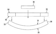
図1,図2に示されるように、多層配線基板10は、コア基板を含まずに形成されたコアレス配線基板であって、第1主面31(図1では上面)及び第2主面32(図1では下面)を有する配線積層部30(積層構造体)を備えている。本実施形態の配線積層部30は、縦50.0mm×横50.0mm×厚さ0.28mmの平面視略矩形状である。
As shown in FIGS. 1 and 2, the
また、配線積層部30は、7層の樹脂絶縁層21,22,23,24,25,26,27と銅からなる6層の導体層28とを交互に積層して多層化した構造を有している。各樹脂絶縁層21〜27は、光硬化性を付与していない樹脂絶縁材料、具体的には熱硬化性エポキシ樹脂の硬化物を主体としたビルドアップ材を用いて形成されている。また、各樹脂絶縁層21〜27のうち、第1層,第5層,第7層の樹脂絶縁層21,25,27が第1の樹脂絶縁層となり、第2層,第3層,第4層,第6層の樹脂絶縁層22,23,24,26が第2の樹脂絶縁層となっている。よって、第1主面31側の最外層の樹脂絶縁層は第1の樹脂絶縁層(第1の樹脂絶縁層27)であり、第2主面32側の最外層の樹脂絶縁層も第1の樹脂絶縁層(第1の樹脂絶縁層21)である。また、第1の樹脂絶縁層21,25,27及び第2の樹脂絶縁層22,23,26は、第2の樹脂絶縁層24を挟んで非対称の態様で配置されている。さらに、第2の樹脂絶縁層24の第1主面31側の領域A1に配置されている樹脂絶縁層(第2の樹脂絶縁層26)よりも、第2の樹脂絶縁層24の第2主面32側の領域A2に配置されている樹脂絶縁層(第2の樹脂絶縁層22,23)の方が多くなっている。即ち、第2の樹脂絶縁層24は、配線積層部30の厚さ方向における中央に位置する基準樹脂絶縁層である。なお、第1の樹脂絶縁層21,25,27及び第2の樹脂絶縁層22〜24,26の厚さは、25μm以上45μm以下であることが好ましく、本実施形態ではそれぞれ40μmに設定されている。よって、第1の樹脂絶縁層21,25,27の厚さ及び第2の樹脂絶縁層22〜24,26の厚さは互いに等しくなっている。
The wiring laminated
なお本実施形態では、第2の樹脂絶縁層22〜24,26が無機材料(無機フィラー)としてガラスフィラー29(図2参照)を含有する一方、第1の樹脂絶縁層21,25,27はガラスフィラー29を含有していない。即ち、第2の樹脂絶縁層22〜24,26は、第1の樹脂絶縁層21,25,27よりも多量のガラスフィラー29を含有している。さらに、第2の樹脂絶縁層22〜24,26は、第1の樹脂絶縁層21,25,27よりも熱膨張係数が小さいビルドアップ材によって形成されている。具体的に言うと、第1の樹脂絶縁層21,25,27を形成するビルドアップ材の硬化後の熱膨張係数は40ppm/℃であり、第2の樹脂絶縁層22〜24,26を形成するビルドアップ材の硬化後の熱膨張係数は20ppm/℃である。また、ガラスフィラー29の熱膨張係数は3ppm/℃であり、導体層28の熱膨張係数は17ppm/℃である。そして、配線積層部30全体の熱膨張係数は22ppm/℃となる。なお、熱膨張係数は、0℃〜ガラス転移温度(Tg)間の測定値の平均値をいう。
In the present embodiment, the second resin insulation layers 22 to 24 and 26 contain a glass filler 29 (see FIG. 2) as an inorganic material (inorganic filler), while the first resin insulation layers 21, 25 and 27 are The
図2に示されるように、配線積層部30を厚さ方向に切断した切断面において、仮想線Lと線分L2との間の領域A2に占める第2の樹脂絶縁層22〜24の厚さの比率が、仮想線Lと線分L1との間の領域A1に占める第2の樹脂絶縁層24,26の厚さの比率よりも大きくなっている。なお、仮想線Lは、第1主面31との距離及び第2主面32との距離が互いに等しくなる箇所に設定されている。換言すると、仮想線Lは、第2の樹脂絶縁層24の厚さ方向における中央位置に設定されている。また、線分L1は第1主面31に属する線分であり、線分L2は第2主面32に属する線分である。なお本実施形態において、領域A1の厚さは、樹脂絶縁層25〜27の全体の厚さ(120μm(=40μm×3))と第2の樹脂絶縁層24の半分の厚さ(20μm(=40μm/2))との合計値(140μm)となっている。また、領域A1に占める第2の樹脂絶縁層24,26の厚さは、第2の樹脂絶縁層26の全体の厚さ(40μm)と第2の樹脂絶縁層24の半分の厚さ(20μm)との合計値(60μm)となっている。よって、領域A1に占める第2の樹脂絶縁層24,26の厚さの比率は、約43%(=(60μm/140μm)×100)となる。一方、領域A2の厚さは、樹脂絶縁層21〜23の全体の厚さ(120μm(=40μm×3))と第2の樹脂絶縁層24の半分の厚さ(20μm)との合計値(140μm)であり、領域A1の厚さと等しくなっている。また、領域A2に占める第2の樹脂絶縁層22〜24の厚さは、第2の樹脂絶縁層22,23の全体の厚さ(80μm(=40μm×2))と第2の樹脂絶縁層24の半分の厚さ(20μm)との合計値(100μm)となっている。よって、領域A2に占める第2の樹脂絶縁層22〜24の厚さの比率は、約71%(=(100μm/140μm)×100)となり、領域A1に占める第2の樹脂絶縁層24,26の比率よりも大きくなる。ゆえに、配線積層部30の第2主面32側(領域A2)の熱膨張係数が18ppm/℃となり、配線積層部30の第1主面31側(領域A1)の熱膨張係数が28ppm/℃となるため、領域A2の熱膨張係数は領域A1の熱膨張係数よりも小さくなる。
As shown in FIG. 2, the thickness of the second resin insulation layers 22 to 24 occupying the region A2 between the virtual line L and the line segment L2 on the cut surface obtained by cutting the wiring laminated
図1,図2に示されるように、各樹脂絶縁層21〜27には、それぞれビア穴33及びビア導体34が設けられている。各ビア穴33は、円錐台形状をなし、各樹脂絶縁層21〜27に対してYAGレーザーまたは炭酸ガスレーザーを用いた穴あけ加工を施すことで形成される。各ビア導体34は、いずれも同一方向に(図1では第2主面32側から第1主面31側に向かうに従って)拡径した形状を有している。また、各ビア導体34は、樹脂絶縁層21〜26に形成された各導体層28、第1の樹脂絶縁層27に形成されたICチップ接続端子41、及び、第1の樹脂絶縁層21に形成された母基板接続端子45を相互に電気的に接続している。
As shown in FIGS. 1 and 2, each
そして、配線積層部30の第2主面32上には、接続対象がマザーボード(母基板)であるBGA(ボールグリッドアレイ)用の複数の母基板接続端子45がアレイ状に配置されている。そして、各母基板接続端子45の表面上には、マザーボード接続用の複数の第2主面側はんだバンプ46が配設されており、各第2主面側はんだバンプ46により、配線積層部30は図示しないマザーボード上に実装される。なお、マザーボードの熱膨張係数は、配線積層部30の熱膨張係数(22ppm/℃)よりも小さい値となっており、具体的には約15ppm/℃に設定されている。即ち本実施形態では、マザーボードと配線積層部30との熱膨張係数差が7.0ppm/℃程度となっている。さらに、マザーボードと配線積層部30の領域A2との熱膨張係数差は、3.0ppm/℃程度となる。
A plurality of mother
一方、図1,図2に示されるように、配線積層部30の第1主面31上には、接続対象がICチップ61である複数のICチップ接続端子41が配置されている。各ICチップ接続端子41は、基板中央部に設けられたチップ搭載領域43においてアレイ状に配置されている。さらに、ICチップ接続端子41の表面上には、複数の第1主面側はんだバンプ42が配設されている。各第1主面側はんだバンプ42は、ICチップ61の面接続端子62に電気的に接続されている。なお、ICチップ61は、縦15.0mm×横15.0mm×厚さ0.8mmの矩形平板状であって、熱膨張係数が4.2ppm/℃のシリコンからなっている。即ち、ICチップ61の熱膨張係数は、配線積層部30の熱膨張係数(22ppm/℃)よりも小さい値となっており、ICチップ61と配線積層部30との熱膨張係数差が17.8ppm/℃となっている。
On the other hand, as shown in FIGS. 1 and 2, a plurality of IC
さらに、配線積層部30の第1主面31側には、補強材であるスティフナ51が接合されている。スティフナ51は、縦50.0mm×横50.0mm×厚さ1.0mmの外形寸法を有し、平面視で全体として矩形枠状をなしている。なお、スティフナ51は、樹脂材料(本実施形態ではエポキシ樹脂)中にガラスクロス57(図2参照)を含有させた複合材料によって形成されている。また、スティフナ51は、配線積層部30を構成する樹脂材料(本実施形態ではエポキシ樹脂)よりも高剛性となっている。具体的に言うと、スティフナ51のヤング率は、配線積層部30のヤング率(約8GPa)よりも大きい値となっており、約30GPaに設定されている。さらに、スティフナ51の熱膨張係数は、配線積層部30の熱膨張係数(22ppm/℃)よりも小さい値となっており、具体的には約16ppm/℃に設定されている。即ち本実施形態では、スティフナ51と配線積層部30との熱膨張係数差が6.0ppm/℃程度となっている。
Further, a
図1,図2に示されるように、スティフナ51は、接触面52と、接触面52の反対側に位置する非接触面53とを有している。接触面52は、第1主面31の外周部(即ち、第1主面31においてチップ搭載領域43を除く領域)に面接触可能となっている。また、スティフナ51には、接触面52の中央部及び非接触面53の中央部にて開口する平面視で矩形状の開口部55が貫通形成されている。開口部55は、ICチップ接続端子41及び第1主面側はんだバンプ42を露出させるようになっている。具体的に言うと、開口部55は、縦20mm×横20mmで、四隅に半径1.5mmのアールを有する断面略正方形状の孔である。
As shown in FIGS. 1 and 2, the
そして、スティフナ51の接触面52は、第1主面31の外周部に対して接着剤50を介して面接合される。なお、本実施形態の接着剤50は、熱膨張係数が約20ppm/℃となるエポキシ系接着剤である。そして、開口部55には、エポキシ樹脂からなるアンダーフィル材63が充填形成されている。具体的に言うと、アンダーフィル材63は、ICチップ61と配線積層部30との隙間や、ICチップ61とスティフナ51との隙間に充填されている。本実施形態では、アンダーフィル材63の熱膨張係数が約25ppm/℃となっている。
The
次に、多層配線基板10の製造方法を説明する。
Next, a method for manufacturing the
まず、十分な強度を有する支持基板(ガラスエポキシ基板など)を準備し、その支持基板上に、樹脂絶縁層21〜27及び導体層28をビルドアップして配線積層部30を形成する。
First, a support substrate (such as a glass epoxy substrate) having sufficient strength is prepared, and the
詳述すると、図3に示されるように、支持基板70上に、エポキシ樹脂からなるシート状の絶縁樹脂基材を貼り付けて下地樹脂絶縁層71を形成することにより、支持基板70及び下地樹脂絶縁層71からなる基材72を得る。そして図4に示されるように、基材72の下地樹脂絶縁層71の上面に積層金属シート体74を配置する。ここで、下地樹脂絶縁層71上に積層金属シート体74を配置することにより、以降の製造工程で積層金属シート体74が下地樹脂絶縁層71から剥れない程度の密着性が確保される。積層金属シート体74は、2枚の銅箔75,76を剥離可能な状態で密着させてなる。具体的には、金属めっき(例えば、クロムめっき、ニッケルめっき、チタンめっき、またはこれらの複合めっき)を介して銅箔75と銅箔76とが配置された積層金属シート体74が形成されている。
More specifically, as shown in FIG. 3, a base
次に、積層金属シート体74上にシート状の絶縁樹脂基材を積層し、真空圧着熱プレス機(図示略)を用いて真空下にて加圧加熱することにより、絶縁樹脂基材を硬化させて第1の樹脂絶縁層21(図5参照)を形成する。そして、例えばエキシマレーザーやUVレーザーや炭酸ガスレーザーなどを用いてレーザー加工を施すことにより、第1の樹脂絶縁層21の所定位置にビア穴33(図5参照)を形成する。次に、各ビア穴33内のスミアを除去するデスミア処理を行う。その後、従来公知の手法に従って無電解銅めっき及び電解銅めっきを行い、ビア穴33内にビア導体34(図5参照)を形成する。さらに、従来公知の手法(例えばセミアディティブ法)によってエッチングを行うことにより、第1の樹脂絶縁層21上に導体層28をパターン形成する(図5参照)。
Next, a sheet-like insulating resin base material is laminated on the
また、樹脂絶縁層22〜27、導体層28及びICチップ接続端子41についても、上述した第1の樹脂絶縁層21及び導体層28と同様の手法によって形成し、第1の樹脂絶縁層21上に積層していく。なお本実施形態では、第1の樹脂絶縁層21,25,27に対しても、第2の樹脂絶縁層22〜24,26に対しても、同じレーザー照射条件でビア穴33を形成し、同じめっき条件でビア導体34を形成する。以上の製造工程によって、基材72上に積層金属シート体74、樹脂絶縁層21〜27、導体層28及びICチップ接続端子41を積層した積層体80が形成される(図6参照)。なお、積層体80において積層金属シート体74上に位置する領域が、多層配線基板10の配線積層部30となる部分である。
In addition, the resin insulating layers 22 to 27, the
次に、積層体80から基材72を除去し、銅箔75を露出させる。具体的に言うと、積層金属シート体74における2枚の銅箔75,76の界面にて剥離して、配線積層部30を基材72から分離する(図7参照)。
Next, the
そして図8に示されるように、配線積層部30(第1の樹脂絶縁層21)の下面上にある銅箔75に対してエッチングによるパターニングを行うことにより、第1の樹脂絶縁層21における下面に母基板接続端子45を形成する。次に、第1の樹脂絶縁層27上に形成された複数のICチップ接続端子41上に、ICチップ接続用の第1主面側はんだバンプ42を形成する。具体的には、図示しないはんだボール搭載装置を用いて各ICチップ接続端子41上にはんだボールを配置した後、はんだボールを所定温度に加熱してリフローすることにより、各ICチップ接続端子41上に第1主面側はんだバンプ42を形成する。同様に、第1の樹脂絶縁層21に形成された複数の母基板接続端子45上に、第2主面側はんだバンプ46を形成する。その結果、多層配線基板10(配線積層部30)が完成する。なお、この時点で、配線積層部30には、第2主面32側が凸となる反りが生じている(図9参照)。
And as FIG. 8 shows, the lower surface in the 1st
また、スティフナ51を作製し、あらかじめ準備しておく。なお開口部55は、スティフナ51に対して座繰りカッター、メカニカルドリル、パンチング装置、YAGレーザー、炭酸ガスレーザー等を用いて孔あけ加工を行うことにより、所定位置にあらかじめ形成される。
A
次に、多層配線基板10とスティフナ51とを位置決めした状態で、配線積層部30の第1主面31にスティフナ51を接合する(図9参照)。詳述すると、まず、多層配線基板10を図示しない支持部材によって支持する。次に、スティフナ51の接触面52に接着剤50を塗布した状態で、第1主面31上にスティフナ51を配置し、接触面52を第1主面31に接触させる。この状態で、例えば150℃程度で加熱処理(キュア)を行って接着剤50を固化させれば、加熱処理後に接着剤50が室温まで冷却されるとともに、スティフナ51が第1主面31に対して接着剤50を介して接合固定される(図2参照)。なお、スティフナ51の接合後の冷却時において、配線積層部30は第1主面31側に反るようになる。
Next, with the
その後、配線積層部30のチップ搭載領域43にICチップ61を載置する(図9参照)。このとき、ICチップ61側の面接続端子62と、配線積層部30側の第1主面側はんだバンプ42とを位置合わせするようにする。そして、加熱して各第1主面側はんだバンプ42をリフローすることにより、面接続端子62と第1主面側はんだバンプ42とが接合され、配線積層部30にICチップ61が搭載される。なお、ICチップ61の接合後の冷却時において、配線積層部30はさらに第1主面31側に反るようになる。その結果、配線積層部30の第2主面32側が凸となる反りが矯正される。この後、開口部55内にアンダーフィル材63となる熱硬化性樹脂を充填しかつ熱硬化させる。
Thereafter, the
従って、本実施形態によれば以下の効果を得ることができる。 Therefore, according to the present embodiment, the following effects can be obtained.
(1)本実施形態の多層配線基板10によれば、配線積層部30が、第1の樹脂絶縁層21,25,27と、第1の樹脂絶縁層21,25,27よりも熱膨張係数が小さいビルドアップ材によって形成された第2の樹脂絶縁層22〜24,26とによって構成されている。よって、樹脂絶縁層21〜27の全てが第1の樹脂絶縁層である場合と比較して、配線積層部30の熱膨張係数が小さくなる。これに伴い、配線積層部30の熱膨張係数がICチップ61やマザーボードの熱膨張係数よりも大きい本実施形態においては、樹脂絶縁層21〜27の全てが第1の樹脂絶縁層である場合と比較して、配線積層部30とICチップ61との熱膨張係数差や、配線積層部30とマザーボードとの熱膨張係数差が小さくなる。その結果、熱膨張係数差に起因する熱応力の影響が軽減されるため、配線積層部30とICチップ61との接続部分や、配線積層部30とマザーボードとの接続部分におけるクラックの発生を防止することができる。
(1) According to the
さらに本実施形態によれば、第2の樹脂絶縁層が、第2の樹脂絶縁層24の第1主面31側の領域A1よりも第2の樹脂絶縁層24の第2主面32側の領域A2に多く配置され、領域A2に占める第2の樹脂絶縁層22〜24の厚さの比率が、領域A1に占める第2の樹脂絶縁層24,26の厚さの比率よりも大きくなっている。その結果、配線積層部30の第2主面32側(領域A2)の熱膨張係数が配線積層部30の第1主面31側(領域A1)の熱膨張係数よりも小さくなるため、配線積層部30の熱膨張係数がマザーボードの熱膨張係数よりも大きい本実施形態においては、領域A2の熱膨張係数をマザーボードの熱膨張係数に近付けることができる。よって、配線積層部30とマザーボードとの熱膨張係数差がよりいっそう小さくなるため、熱膨張係数差に起因する熱応力の影響がよりいっそう軽減される。その結果、一般的にマザーボードとの接続面積が大きく、アンダーフィル材などが存在しないためにクラックが発生しやすい部分(配線積層部30とマザーボードとの接続部分)において、クラックの発生を確実に防止することができる。ゆえに、歩留まりが高くなり、多層配線基板10の信頼性が向上する。
Further, according to the present embodiment, the second resin insulation layer is closer to the second
(2)本実施形態では、敢えて第2主面32側が凸となる反りが生じている配線積層部30(図9参照)を作製している。このため、配線積層部30の熱膨張係数がICチップ61の熱膨張係数よりも大きい本実施形態においては、ICチップ接続端子41にICチップ61を接続した際に、ICチップ61の材料と配線積層部30の材料との熱膨張係数差に起因する熱応力の影響を受けて、配線積層部30が第1主面31側に反るようになる。その結果、配線積層部30の第2主面32側が凸となる反りが矯正される。よって、ICチップ61の接続後に反りのない多層配線基板10を作製することができる。
(2) In the present embodiment, the wiring laminated portion 30 (see FIG. 9) in which a warp in which the second
なお、本実施形態を以下のように変更してもよい。 In addition, you may change this embodiment as follows.
・上記実施形態の配線積層部30では、領域A1に第2の樹脂絶縁層26全体と第2の樹脂絶縁層24の上半分とを配置するとともに、領域A2に第2の樹脂絶縁層22,23全体と第2の樹脂絶縁層24の下半分とを配置することにより、領域A2に占める第2の樹脂絶縁層22〜24の厚さの比率を、領域A1に占める第2の樹脂絶縁層24,26の厚さの比率よりも大きくしていた。しかし図10に示されるように、領域A1に第2の樹脂絶縁層221の上半分のみを配置するとともに、領域A2に第2の樹脂絶縁層222全体と第2の樹脂絶縁層221の下半分を配置することにより、領域A2に占める第2の樹脂絶縁層221,222の厚さの比率を領域A1に占める第2の樹脂絶縁層221の厚さの比率よりも大きくした配線積層部230であってもよい。また図11に示されるように、領域A2に第2の樹脂絶縁層321を配置する一方、領域A1に第2の樹脂絶縁層を配置しないことにより、領域A2に占める第2の樹脂絶縁層321の厚さの比率を領域A1に占める第2の樹脂絶縁層の厚さの比率よりも大きくした配線積層部330であってもよい。なお、配線積層部330では、第2の樹脂絶縁層ではなく、第1の樹脂絶縁層322が基準樹脂絶縁層として用いられている。
-In the wiring laminated
・上記実施形態の配線積層部30では、第1の樹脂絶縁層21,25,27の厚さと第2の樹脂絶縁層22〜24,26の厚さとが互いに等しくなっていた。しかし、例えば図12に示されるように、第1の樹脂絶縁層121,122,123の厚さと第2の樹脂絶縁層124の厚さとが互いに異なる配線積層部130であってもよい。なお、第2の樹脂絶縁層124の厚さは、例えば、第1の樹脂絶縁層121〜123の厚さの1.2倍以上2.0倍以下であることが好ましい。図12に示す配線積層部130では、第1の樹脂絶縁層121〜123の厚さがそれぞれ40μmに設定され、第2の樹脂絶縁層124の厚さが60μmに設定されている。
-In the wiring laminated
・上記実施形態では、第2の樹脂絶縁層22〜24,26が無機材料としてガラスフィラー29を含有する一方、第1の樹脂絶縁層21,25,27は無機材料を何ら含有していなかった。しかし、第1の樹脂絶縁層21,25,27に無機材料を含有させるとともに、第2の樹脂絶縁層22〜24,26に第1の樹脂絶縁層21,25,27よりも多量の無機材料を含有させるようにしてもよい。
In the above embodiment, the second resin insulation layers 22 to 24 and 26 contain the
・上記実施形態の第2の樹脂絶縁層22〜24,26は、ガラスフィラー29を無機材料として含有していたが、その代わりにガラスクロス(無機繊維クロス)を無機材料として含有させてもよい。このようにすれば、第2の樹脂絶縁層22〜24,26全体の熱膨張係数が大きく低下するため、第2の樹脂絶縁層22〜24,26を形成するビルドアップ材の熱膨張係数をさほど小さくしなくても済む。なお、第2の樹脂絶縁層22〜24,26にガラスクロスを含有させる場合、ビルドアップ材としての機能(他の樹脂絶縁層との密着性、導体層28同士の絶縁性)を持たせるためには、一定量の樹脂絶縁材料を確保する必要がある。よって、第2の樹脂絶縁層22〜24,26は、ガラスクロスの厚さ分(15μm程度)だけ厚くなる。
-Although the 2nd resin insulation layers 22-24, 26 of the said embodiment contained the
・上記実施形態では、スティフナ51の熱膨張係数(約16ppm/℃)が配線積層部30の熱膨張係数(22ppm/℃)よりも小さくなっており、第2の樹脂絶縁層が領域A1よりも領域A2に多く配置されていた。しかし、スティフナ51の熱膨張係数が配線積層部30の熱膨張係数よりも大きい場合、領域A1に配置される第2の樹脂絶縁層の枚数を増やしてもよい。なお、スティフナ51は省略されていてもよい。
In the above embodiment, the coefficient of thermal expansion (about 16 ppm / ° C.) of the
・上記実施形態では、複数の樹脂絶縁層21〜27に形成されたビア導体34は、いずれも第2主面32側から第1主面31側に向かうに従って拡径した形状を有していたが、これに限定されるものではない。複数の樹脂絶縁層21〜27に形成されるビア導体34は同一方向に拡径した形状であればよく、第1主面31側から第2主面32側に向かうに従って拡径した形状を有していてもよい。
In the above embodiment, each of the via
・上記実施形態において、第1の樹脂絶縁層27の表面及び第1の樹脂絶縁層21の下面の少なくとも一方を、ソルダーレジストによってほぼ全体的に覆うようにしてもよい。なお、第1の樹脂絶縁層27の表面を覆うソルダーレジストの所定箇所には、ICチップ接続端子41を露出させる開口部が形成され、第1の樹脂絶縁層21の下面を覆うソルダーレジストの所定箇所には、母基板接続端子45を露出させる開口部が形成される。
In the embodiment described above, at least one of the surface of the first
・上記実施形態の配線積層部30は、7層の樹脂絶縁層21〜27を積層することによって構成されていたが、6層以下の樹脂絶縁層によって構成されていてもよいし、8層以上の樹脂絶縁層によって構成されていてもよい。
-Although the wiring lamination | stacking
次に、前述した実施形態によって把握される技術的思想を以下に列挙する。 Next, the technical ideas grasped by the embodiment described above are listed below.
(1)上記手段1または2において、前記第1の樹脂絶縁層の厚さと前記第2の樹脂絶縁層の厚さとが互いに異なることを特徴とする多層配線基板。 (1) The multilayer wiring board according to the above means 1 or 2, wherein the thickness of the first resin insulation layer and the thickness of the second resin insulation layer are different from each other.
(2)技術的思想(1)において、前記第2の樹脂絶縁層の厚さは、前記第1の樹脂絶縁層の厚さの1.2倍以上2.0倍以下であることを特徴とする多層配線基板。 (2) In the technical idea (1), the thickness of the second resin insulation layer is 1.2 times or more and 2.0 times or less the thickness of the first resin insulation layer. Multilayer wiring board.
(3)上記手段1または2において、前記第1の樹脂絶縁層の厚さと前記第2の樹脂絶縁層の厚さとが互いに等しいことを特徴とする多層配線基板。 (3) In the above means 1 or 2, the multilayer wiring board is characterized in that the thickness of the first resin insulation layer and the thickness of the second resin insulation layer are equal to each other.
(4)上記手段1または2において、前記第1の樹脂絶縁層及び前記第2の樹脂絶縁層の厚さは、25μm以上45μm以下であることを特徴とする多層配線基板。 (4) In the above means 1 or 2, the multilayer wiring board is characterized in that the thickness of the first resin insulating layer and the second resin insulating layer is 25 μm or more and 45 μm or less.
(5)上記手段1または2において、前記第1主面側に、前記複数のICチップ接続端子を露出させる開口部が貫通形成されるとともに、平面視で全体として枠状をなす補強材が接合され、前記開口部内にアンダーフィル材が充填されていることを特徴とする多層配線基板。 (5) In the above means 1 or 2, an opening for exposing the plurality of IC chip connection terminals is formed through the first main surface side, and a reinforcing material having a frame shape in plan view is joined. A multilayer wiring board, wherein the opening is filled with an underfill material.
10…多層配線基板
21,25,27,121,122,123…樹脂絶縁層としての第1の樹脂絶縁層
322…樹脂絶縁層及び基準樹脂絶縁層としての第1の樹脂絶縁層
22,23,26,124,222,321…樹脂絶縁層としての第2の樹脂絶縁層
24,221…樹脂絶縁層及び基準樹脂絶縁層としての第2の樹脂絶縁層
28…導体層
29…無機材料及び無機フィラーとしてのガラスフィラー
30,130,230,330…積層構造体としての配線積層部
31…第1主面
32…第2主面
34…ビア導体
41…ICチップ接続端子
45…母基板接続端子
51…補強材としてのスティフナ
61…ICチップ
A1…仮想線と第1主面に属する線分との間の領域(基準樹脂絶縁層の第1主面側の領域)
A2…仮想線と第2主面に属する線分との間の領域(基準樹脂絶縁層の第2主面側の領域)
L…仮想線
L1…第1主面に属する線分
L2…第2主面に属する線分
DESCRIPTION OF
A2... Region between the virtual line and the line segment belonging to the second main surface (region on the second main surface side of the reference resin insulating layer)
L ... Virtual line L1 ... Line segment belonging to the first main surface L2 ... Line segment belonging to the second main surface
Claims (1)
前記複数の樹脂絶縁層は、樹脂絶縁材料を主体としたビルドアップ材によって形成された第1の樹脂絶縁層と、前記第1の樹脂絶縁層よりも多量の無機材料を含有しかつ前記第1の樹脂絶縁層よりも熱膨張係数が小さいビルドアップ材によって形成された第2の樹脂絶縁層とを含み、
前記第2の樹脂絶縁層は、無機フィラー及び無機繊維クロスの少なくとも一方を前記無機材料として含有しており、
前記第1主面側の最外層の樹脂絶縁層及び前記第2主面側の最外層の樹脂絶縁層の少なくとも一方は、前記第1の樹脂絶縁層であり、
前記積層構造体の厚さ方向における中央に、複数の前記第2の樹脂絶縁層からなる積層体が配置され、前記積層体の前記第1主面側に、前記第1の樹脂絶縁層を介して前記第2の樹脂絶縁層がさらに積層され、
前記積層構造体を厚さ方向に切断した切断面において、前記第1主面との距離及び前記第2主面との距離が互いに等しくなる箇所に設定された仮想線と前記第2主面に属する線分との間の領域に占める前記第2の樹脂絶縁層の厚さの比率が、前記仮想線と前記第1主面に属する線分との間の領域に占める前記第2の樹脂絶縁層の厚さの比率よりも大きくなっており、
前記積層構造体には、前記第2主面側が凸となる反りが生じており、
前記第1主面側に、前記複数のICチップ接続端子を露出させるとともに、平面視で全体として枠状をなす補強材が接合される
ことを特徴とする多層配線基板。 A plurality of IC chip connections having a multilayer structure in which a plurality of resin insulation layers and a plurality of conductor layers are alternately stacked, and the connection target is an IC chip on the first main surface side of the multilayer structure Terminals are arranged, and a plurality of mother board connection terminals whose connection target is a mother board are arranged on the second main surface side of the multilayer structure, and the plurality of conductor layers are formed on the plurality of resin insulating layers. In either case, the diameter is increased from the second main surface side toward the first main surface side, or the diameter is increased from the first main surface side toward the second main surface side. A multilayer wiring board connected by via conductors having
The plurality of resin insulation layers include a first resin insulation layer formed of a build-up material mainly composed of a resin insulation material, a larger amount of inorganic material than the first resin insulation layer, and the first resin insulation layer. A second resin insulation layer formed of a build-up material having a smaller thermal expansion coefficient than the resin insulation layer of
The second resin insulation layer contains at least one of an inorganic filler and an inorganic fiber cloth as the inorganic material,
At least one of the outermost resin insulating layer on the first main surface side and the outermost resin insulating layer on the second main surface side is the first resin insulating layer,
A laminated body composed of a plurality of the second resin insulation layers is disposed at the center in the thickness direction of the laminated structure, and the first resin insulation layer is interposed on the first main surface side of the laminated body. The second resin insulation layer is further laminated,
In the cut surface obtained by cutting the laminated structure in the thickness direction, a virtual line set at a location where the distance from the first main surface and the distance from the second main surface are equal to each other and the second main surface The ratio of the thickness of the second resin insulation layer occupying the area between the line segment belonging to the second resin insulation layer occupying the area between the virtual line and the line segment belonging to the first main surface. Is larger than the ratio of the thickness of the layers,
In the laminated structure, there is a warp that the second main surface side is convex ,
The multilayer wiring board , wherein the plurality of IC chip connection terminals are exposed to the first main surface side, and a reinforcing material having a frame shape as a whole is joined in plan view .
Priority Applications (5)
| Application Number | Priority Date | Filing Date | Title |
|---|---|---|---|
| JP2010173305A JP5079059B2 (en) | 2010-08-02 | 2010-08-02 | Multilayer wiring board |
| TW100126899A TWI461117B (en) | 2010-08-02 | 2011-07-29 | Multilayer wiring substrate |
| US13/195,290 US8530751B2 (en) | 2010-08-02 | 2011-08-01 | Multilayer wiring substrate |
| KR1020110076655A KR101322126B1 (en) | 2010-08-02 | 2011-08-01 | Multilayer Wiring Substrate |
| CN201110225099.1A CN102347287B (en) | 2010-08-02 | 2011-08-02 | Multilayer wiring substrate |
Applications Claiming Priority (1)
| Application Number | Priority Date | Filing Date | Title |
|---|---|---|---|
| JP2010173305A JP5079059B2 (en) | 2010-08-02 | 2010-08-02 | Multilayer wiring board |
Related Child Applications (1)
| Application Number | Title | Priority Date | Filing Date |
|---|---|---|---|
| JP2012005848A Division JP5449413B2 (en) | 2012-01-16 | 2012-01-16 | Multilayer wiring board |
Publications (3)
| Publication Number | Publication Date |
|---|---|
| JP2012033790A JP2012033790A (en) | 2012-02-16 |
| JP2012033790A5 JP2012033790A5 (en) | 2012-05-10 |
| JP5079059B2 true JP5079059B2 (en) | 2012-11-21 |
Family
ID=45525552
Family Applications (1)
| Application Number | Title | Priority Date | Filing Date |
|---|---|---|---|
| JP2010173305A Expired - Fee Related JP5079059B2 (en) | 2010-08-02 | 2010-08-02 | Multilayer wiring board |
Country Status (5)
| Country | Link |
|---|---|
| US (1) | US8530751B2 (en) |
| JP (1) | JP5079059B2 (en) |
| KR (1) | KR101322126B1 (en) |
| CN (1) | CN102347287B (en) |
| TW (1) | TWI461117B (en) |
Families Citing this family (34)
| Publication number | Priority date | Publication date | Assignee | Title |
|---|---|---|---|---|
| US8780576B2 (en) * | 2011-09-14 | 2014-07-15 | Invensas Corporation | Low CTE interposer |
| KR101939236B1 (en) * | 2011-11-10 | 2019-01-16 | 삼성전자 주식회사 | Substrate and electronic device comprising the same |
| US9159649B2 (en) * | 2011-12-20 | 2015-10-13 | Intel Corporation | Microelectronic package and stacked microelectronic assembly and computing system containing same |
| US9117730B2 (en) * | 2011-12-29 | 2015-08-25 | Ibiden Co., Ltd. | Printed wiring board and method for manufacturing printed wiring board |
| KR101331669B1 (en) * | 2012-03-08 | 2013-11-20 | 삼성전기주식회사 | Substrate for power module |
| JP5955102B2 (en) * | 2012-05-29 | 2016-07-20 | 京セラ株式会社 | Wiring board and manufacturing method thereof |
| US9615447B2 (en) * | 2012-07-23 | 2017-04-04 | Zhuhai Advanced Chip Carriers & Electronic Substrate Solutions Technologies Co. Ltd. | Multilayer electronic support structure with integral constructional elements |
| TW201409633A (en) * | 2012-08-24 | 2014-03-01 | Kinsus Interconnect Tech Corp | Encapsulation structure of chip and carrier board |
| JP2014063844A (en) * | 2012-09-20 | 2014-04-10 | Sony Corp | Semiconductor device, semiconductor device manufacturing method and electronic apparatus |
| US8802504B1 (en) | 2013-03-14 | 2014-08-12 | Taiwan Semiconductor Manufacturing Company, Ltd. | 3D packages and methods for forming the same |
| US9299649B2 (en) | 2013-02-08 | 2016-03-29 | Taiwan Semiconductor Manufacturing Company, Ltd. | 3D packages and methods for forming the same |
| CN104218016A (en) * | 2013-06-04 | 2014-12-17 | 宏启胜精密电子(秦皇岛)有限公司 | IC (integrated circuit) carrier board and semiconductor device with same |
| KR102149793B1 (en) * | 2013-10-24 | 2020-08-31 | 삼성전기주식회사 | Printed circuit board and control method of warpage of printed circuit board |
| WO2016103359A1 (en) * | 2014-12-24 | 2016-06-30 | ルネサスエレクトロニクス株式会社 | Semiconductor device |
| US20160205778A1 (en) * | 2015-01-14 | 2016-07-14 | Bridge Semiconductor Corporation | Wiring board with embedded interposer integrated with stiffener and method of making the same |
| US20160204056A1 (en) * | 2015-01-14 | 2016-07-14 | Bridge Semiconductor Corporation | Wiring board with interposer and dual wiring structures integrated together and method of making the same |
| CN105870075A (en) * | 2015-01-22 | 2016-08-17 | 恒劲科技股份有限公司 | Substrate structure |
| CN106034374B (en) * | 2015-03-12 | 2018-10-16 | 日立汽车系统(苏州)有限公司 | Anti- substrate deformation structure |
| TWI603505B (en) * | 2015-04-07 | 2017-10-21 | 矽品精密工業股份有限公司 | Package substrate |
| JP2016219452A (en) * | 2015-05-14 | 2016-12-22 | 富士通株式会社 | Multilayer substrate and manufacturing method for multilayer substrate |
| US10109588B2 (en) * | 2015-05-15 | 2018-10-23 | Samsung Electro-Mechanics Co., Ltd. | Electronic component package and package-on-package structure including the same |
| JP2016219478A (en) * | 2015-05-15 | 2016-12-22 | イビデン株式会社 | Wiring board and manufacturing method therefor |
| WO2017051809A1 (en) * | 2015-09-25 | 2017-03-30 | 大日本印刷株式会社 | Mounting component, wiring board, electronic device, and methods for manufacturing same |
| KR102512228B1 (en) * | 2015-10-01 | 2023-03-21 | 삼성전기주식회사 | Insulating material and printed circuit board having the same |
| US9711458B2 (en) * | 2015-11-13 | 2017-07-18 | Taiwan Semiconductor Manufacturing Company, Ltd. | Structure and formation method for chip package |
| KR101912278B1 (en) | 2015-12-21 | 2018-10-29 | 삼성전기 주식회사 | Electronic component package and manufactruing method of the same |
| TWI563602B (en) * | 2016-04-15 | 2016-12-21 | Phoenix Pioneer Technology Co Ltd | Method of fabricating a package substrate |
| US9761535B1 (en) * | 2016-06-27 | 2017-09-12 | Nanya Technology Corporation | Interposer, semiconductor package with the same and method for preparing a semiconductor package with the same |
| KR102456322B1 (en) * | 2017-11-08 | 2022-10-19 | 삼성전기주식회사 | Substrate strip and electronic component package having the same |
| US10242964B1 (en) | 2018-01-16 | 2019-03-26 | Bridge Semiconductor Corp. | Wiring substrate for stackable semiconductor assembly and stackable semiconductor assembly using the same |
| TWI655739B (en) * | 2018-04-19 | 2019-04-01 | 南亞電路板股份有限公司 | Package structure and forming method thereof |
| JP7099359B2 (en) | 2019-02-20 | 2022-07-12 | 株式会社村田製作所 | Coil parts |
| US11094649B2 (en) * | 2020-01-21 | 2021-08-17 | Advanced Semiconductor Engineering, Inc. | Semiconductor package structure and method for manufacturing the same |
| US11233035B2 (en) * | 2020-05-28 | 2022-01-25 | Taiwan Semiconductor Manufacturing Company, Ltd. | Package structure and method of manufacturing the same |
Family Cites Families (12)
| Publication number | Priority date | Publication date | Assignee | Title |
|---|---|---|---|---|
| JP2004356569A (en) | 2003-05-30 | 2004-12-16 | Shinko Electric Ind Co Ltd | Package for semiconductor device |
| JP4342366B2 (en) * | 2004-04-09 | 2009-10-14 | 日本特殊陶業株式会社 | Wiring board manufacturing method |
| JP2006287056A (en) * | 2005-04-01 | 2006-10-19 | Ngk Spark Plug Co Ltd | Wiring board and method of manufacturing the same |
| JP2008078683A (en) | 2005-08-29 | 2008-04-03 | Shinko Electric Ind Co Ltd | Multilayer wiring board |
| JP4072176B2 (en) | 2005-08-29 | 2008-04-09 | 新光電気工業株式会社 | Manufacturing method of multilayer wiring board |
| JP2008118155A (en) | 2007-12-20 | 2008-05-22 | Shinko Electric Ind Co Ltd | Package for semiconductor device |
| JP2008118154A (en) | 2007-12-20 | 2008-05-22 | Shinko Electric Ind Co Ltd | Package for semiconductor device |
| JP5179920B2 (en) * | 2008-03-28 | 2013-04-10 | 日本特殊陶業株式会社 | Multilayer wiring board |
| JP5290017B2 (en) * | 2008-03-28 | 2013-09-18 | 日本特殊陶業株式会社 | Multilayer wiring board and manufacturing method thereof |
| TWI475932B (en) | 2008-09-29 | 2015-03-01 | Ngk Spark Plug Co | Wiring substrate with reinforcement |
| JP5306789B2 (en) * | 2008-12-03 | 2013-10-02 | 日本特殊陶業株式会社 | Multilayer wiring board and manufacturing method thereof |
| JP4473935B1 (en) * | 2009-07-06 | 2010-06-02 | 新光電気工業株式会社 | Multilayer wiring board |
-
2010
- 2010-08-02 JP JP2010173305A patent/JP5079059B2/en not_active Expired - Fee Related
-
2011
- 2011-07-29 TW TW100126899A patent/TWI461117B/en not_active IP Right Cessation
- 2011-08-01 US US13/195,290 patent/US8530751B2/en not_active Expired - Fee Related
- 2011-08-01 KR KR1020110076655A patent/KR101322126B1/en not_active IP Right Cessation
- 2011-08-02 CN CN201110225099.1A patent/CN102347287B/en not_active Expired - Fee Related
Also Published As
| Publication number | Publication date |
|---|---|
| US8530751B2 (en) | 2013-09-10 |
| CN102347287B (en) | 2015-01-28 |
| TWI461117B (en) | 2014-11-11 |
| US20120024582A1 (en) | 2012-02-02 |
| CN102347287A (en) | 2012-02-08 |
| KR101322126B1 (en) | 2013-10-28 |
| KR20120022593A (en) | 2012-03-12 |
| TW201220980A (en) | 2012-05-16 |
| JP2012033790A (en) | 2012-02-16 |
Similar Documents
| Publication | Publication Date | Title |
|---|---|---|
| JP5079059B2 (en) | Multilayer wiring board | |
| JP5284235B2 (en) | Semiconductor package | |
| JP5289996B2 (en) | Reinforced wiring board | |
| JP5356876B2 (en) | Multilayer wiring board and manufacturing method thereof | |
| JP5284147B2 (en) | Multilayer wiring board | |
| JP5290017B2 (en) | Multilayer wiring board and manufacturing method thereof | |
| JP5179920B2 (en) | Multilayer wiring board | |
| JP5902931B2 (en) | WIRING BOARD MANUFACTURING METHOD AND WIRING BOARD MANUFACTURING SUPPORT | |
| JP5367523B2 (en) | Wiring board and method of manufacturing wiring board | |
| JP5172404B2 (en) | Multilayer wiring board manufacturing method and multilayer wiring board intermediate product | |
| JP2015211194A (en) | Printed wiring board, semiconductor package and printed wiring board manufacturing method | |
| JP5260215B2 (en) | Manufacturing method of wiring board with reinforcing material | |
| JP5129783B2 (en) | Wiring board with reinforcing material and method for manufacturing the same | |
| JP5306879B2 (en) | Reinforced wiring board | |
| JP5449413B2 (en) | Multilayer wiring board | |
| JP5340622B2 (en) | Multilayer wiring board | |
| JP5350829B2 (en) | Manufacturing method of wiring board with reinforcing material, wiring board for wiring board with reinforcing material | |
| JP5330286B2 (en) | Manufacturing method of wiring board with reinforcing material | |
| JP2004214271A (en) | Single side lamination wiring board and its manufacturing method | |
| JP5356883B2 (en) | Manufacturing method of wiring board with reinforcing material | |
| TWI507109B (en) | A supporting substrate for manufacturing a multilayer wiring board, and a method for manufacturing the multilayer wiring board |
Legal Events
| Date | Code | Title | Description |
|---|---|---|---|
| A621 | Written request for application examination |
Free format text: JAPANESE INTERMEDIATE CODE: A621 Effective date: 20120116 |
|
| A521 | Request for written amendment filed |
Free format text: JAPANESE INTERMEDIATE CODE: A523 Effective date: 20120316 |
|
| A131 | Notification of reasons for refusal |
Free format text: JAPANESE INTERMEDIATE CODE: A131 Effective date: 20120515 |
|
| A977 | Report on retrieval |
Free format text: JAPANESE INTERMEDIATE CODE: A971007 Effective date: 20120517 |
|
| A521 | Request for written amendment filed |
Free format text: JAPANESE INTERMEDIATE CODE: A523 Effective date: 20120709 |
|
| TRDD | Decision of grant or rejection written | ||
| A01 | Written decision to grant a patent or to grant a registration (utility model) |
Free format text: JAPANESE INTERMEDIATE CODE: A01 Effective date: 20120807 |
|
| A01 | Written decision to grant a patent or to grant a registration (utility model) |
Free format text: JAPANESE INTERMEDIATE CODE: A01 |
|
| A61 | First payment of annual fees (during grant procedure) |
Free format text: JAPANESE INTERMEDIATE CODE: A61 Effective date: 20120828 |
|
| FPAY | Renewal fee payment (event date is renewal date of database) |
Free format text: PAYMENT UNTIL: 20150907 Year of fee payment: 3 |
|
| R150 | Certificate of patent or registration of utility model |
Free format text: JAPANESE INTERMEDIATE CODE: R150 |
|
| R250 | Receipt of annual fees |
Free format text: JAPANESE INTERMEDIATE CODE: R250 |
|
| LAPS | Cancellation because of no payment of annual fees |