JP5079059B2 - 多層配線基板 - Google Patents
多層配線基板 Download PDFInfo
- Publication number
- JP5079059B2 JP5079059B2 JP2010173305A JP2010173305A JP5079059B2 JP 5079059 B2 JP5079059 B2 JP 5079059B2 JP 2010173305 A JP2010173305 A JP 2010173305A JP 2010173305 A JP2010173305 A JP 2010173305A JP 5079059 B2 JP5079059 B2 JP 5079059B2
- Authority
- JP
- Japan
- Prior art keywords
- main surface
- resin insulation
- resin
- insulation layer
- surface side
- Prior art date
- Legal status (The legal status is an assumption and is not a legal conclusion. Google has not performed a legal analysis and makes no representation as to the accuracy of the status listed.)
- Expired - Fee Related
Links
Images


Classifications
-
- H—ELECTRICITY
- H01—ELECTRIC ELEMENTS
- H01L—SEMICONDUCTOR DEVICES NOT COVERED BY CLASS H10
- H01L23/00—Details of semiconductor or other solid state devices
- H01L23/48—Arrangements for conducting electric current to or from the solid state body in operation, e.g. leads, terminal arrangements ; Selection of materials therefor
- H01L23/488—Arrangements for conducting electric current to or from the solid state body in operation, e.g. leads, terminal arrangements ; Selection of materials therefor consisting of soldered or bonded constructions
- H01L23/498—Leads, i.e. metallisations or lead-frames on insulating substrates, e.g. chip carriers
- H01L23/49822—Multilayer substrates
-
- H—ELECTRICITY
- H01—ELECTRIC ELEMENTS
- H01L—SEMICONDUCTOR DEVICES NOT COVERED BY CLASS H10
- H01L23/00—Details of semiconductor or other solid state devices
- H01L23/32—Holders for supporting the complete device in operation, i.e. detachable fixtures
-
- H—ELECTRICITY
- H01—ELECTRIC ELEMENTS
- H01L—SEMICONDUCTOR DEVICES NOT COVERED BY CLASS H10
- H01L21/00—Processes or apparatus adapted for the manufacture or treatment of semiconductor or solid state devices or of parts thereof
- H01L21/02—Manufacture or treatment of semiconductor devices or of parts thereof
- H01L21/04—Manufacture or treatment of semiconductor devices or of parts thereof the devices having at least one potential-jump barrier or surface barrier, e.g. PN junction, depletion layer or carrier concentration layer
- H01L21/48—Manufacture or treatment of parts, e.g. containers, prior to assembly of the devices, using processes not provided for in a single one of the subgroups H01L21/06 - H01L21/326
- H01L21/4814—Conductive parts
- H01L21/4846—Leads on or in insulating or insulated substrates, e.g. metallisation
- H01L21/4857—Multilayer substrates
-
- H—ELECTRICITY
- H01—ELECTRIC ELEMENTS
- H01L—SEMICONDUCTOR DEVICES NOT COVERED BY CLASS H10
- H01L23/00—Details of semiconductor or other solid state devices
- H01L23/12—Mountings, e.g. non-detachable insulating substrates
-
- H—ELECTRICITY
- H01—ELECTRIC ELEMENTS
- H01L—SEMICONDUCTOR DEVICES NOT COVERED BY CLASS H10
- H01L23/00—Details of semiconductor or other solid state devices
- H01L23/12—Mountings, e.g. non-detachable insulating substrates
- H01L23/14—Mountings, e.g. non-detachable insulating substrates characterised by the material or its electrical properties
- H01L23/145—Organic substrates, e.g. plastic
-
- H—ELECTRICITY
- H01—ELECTRIC ELEMENTS
- H01L—SEMICONDUCTOR DEVICES NOT COVERED BY CLASS H10
- H01L23/00—Details of semiconductor or other solid state devices
- H01L23/48—Arrangements for conducting electric current to or from the solid state body in operation, e.g. leads, terminal arrangements ; Selection of materials therefor
- H01L23/488—Arrangements for conducting electric current to or from the solid state body in operation, e.g. leads, terminal arrangements ; Selection of materials therefor consisting of soldered or bonded constructions
- H01L23/498—Leads, i.e. metallisations or lead-frames on insulating substrates, e.g. chip carriers
- H01L23/49811—Additional leads joined to the metallisation on the insulating substrate, e.g. pins, bumps, wires, flat leads
- H01L23/49816—Spherical bumps on the substrate for external connection, e.g. ball grid arrays [BGA]
-
- H—ELECTRICITY
- H01—ELECTRIC ELEMENTS
- H01L—SEMICONDUCTOR DEVICES NOT COVERED BY CLASS H10
- H01L23/00—Details of semiconductor or other solid state devices
- H01L23/48—Arrangements for conducting electric current to or from the solid state body in operation, e.g. leads, terminal arrangements ; Selection of materials therefor
- H01L23/488—Arrangements for conducting electric current to or from the solid state body in operation, e.g. leads, terminal arrangements ; Selection of materials therefor consisting of soldered or bonded constructions
- H01L23/498—Leads, i.e. metallisations or lead-frames on insulating substrates, e.g. chip carriers
- H01L23/49833—Leads, i.e. metallisations or lead-frames on insulating substrates, e.g. chip carriers the chip support structure consisting of a plurality of insulating substrates
-
- H—ELECTRICITY
- H01—ELECTRIC ELEMENTS
- H01L—SEMICONDUCTOR DEVICES NOT COVERED BY CLASS H10
- H01L23/00—Details of semiconductor or other solid state devices
- H01L23/52—Arrangements for conducting electric current within the device in operation from one component to another, i.e. interconnections, e.g. wires, lead frames
-
- H—ELECTRICITY
- H05—ELECTRIC TECHNIQUES NOT OTHERWISE PROVIDED FOR
- H05K—PRINTED CIRCUITS; CASINGS OR CONSTRUCTIONAL DETAILS OF ELECTRIC APPARATUS; MANUFACTURE OF ASSEMBLAGES OF ELECTRICAL COMPONENTS
- H05K3/00—Apparatus or processes for manufacturing printed circuits
- H05K3/46—Manufacturing multilayer circuits
- H05K3/4644—Manufacturing multilayer circuits by building the multilayer layer by layer, i.e. build-up multilayer circuits
- H05K3/4682—Manufacture of core-less build-up multilayer circuits on a temporary carrier or on a metal foil
-
- H—ELECTRICITY
- H01—ELECTRIC ELEMENTS
- H01L—SEMICONDUCTOR DEVICES NOT COVERED BY CLASS H10
- H01L2224/00—Indexing scheme for arrangements for connecting or disconnecting semiconductor or solid-state bodies and methods related thereto as covered by H01L24/00
- H01L2224/01—Means for bonding being attached to, or being formed on, the surface to be connected, e.g. chip-to-package, die-attach, "first-level" interconnects; Manufacturing methods related thereto
- H01L2224/10—Bump connectors; Manufacturing methods related thereto
- H01L2224/15—Structure, shape, material or disposition of the bump connectors after the connecting process
- H01L2224/16—Structure, shape, material or disposition of the bump connectors after the connecting process of an individual bump connector
- H01L2224/161—Disposition
- H01L2224/16151—Disposition the bump connector connecting between a semiconductor or solid-state body and an item not being a semiconductor or solid-state body, e.g. chip-to-substrate, chip-to-passive
- H01L2224/16221—Disposition the bump connector connecting between a semiconductor or solid-state body and an item not being a semiconductor or solid-state body, e.g. chip-to-substrate, chip-to-passive the body and the item being stacked
- H01L2224/16225—Disposition the bump connector connecting between a semiconductor or solid-state body and an item not being a semiconductor or solid-state body, e.g. chip-to-substrate, chip-to-passive the body and the item being stacked the item being non-metallic, e.g. insulating substrate with or without metallisation
-
- H—ELECTRICITY
- H01—ELECTRIC ELEMENTS
- H01L—SEMICONDUCTOR DEVICES NOT COVERED BY CLASS H10
- H01L2224/00—Indexing scheme for arrangements for connecting or disconnecting semiconductor or solid-state bodies and methods related thereto as covered by H01L24/00
- H01L2224/01—Means for bonding being attached to, or being formed on, the surface to be connected, e.g. chip-to-package, die-attach, "first-level" interconnects; Manufacturing methods related thereto
- H01L2224/26—Layer connectors, e.g. plate connectors, solder or adhesive layers; Manufacturing methods related thereto
- H01L2224/31—Structure, shape, material or disposition of the layer connectors after the connecting process
- H01L2224/32—Structure, shape, material or disposition of the layer connectors after the connecting process of an individual layer connector
- H01L2224/321—Disposition
- H01L2224/32151—Disposition the layer connector connecting between a semiconductor or solid-state body and an item not being a semiconductor or solid-state body, e.g. chip-to-substrate, chip-to-passive
- H01L2224/32221—Disposition the layer connector connecting between a semiconductor or solid-state body and an item not being a semiconductor or solid-state body, e.g. chip-to-substrate, chip-to-passive the body and the item being stacked
- H01L2224/32225—Disposition the layer connector connecting between a semiconductor or solid-state body and an item not being a semiconductor or solid-state body, e.g. chip-to-substrate, chip-to-passive the body and the item being stacked the item being non-metallic, e.g. insulating substrate with or without metallisation
-
- H—ELECTRICITY
- H01—ELECTRIC ELEMENTS
- H01L—SEMICONDUCTOR DEVICES NOT COVERED BY CLASS H10
- H01L2224/00—Indexing scheme for arrangements for connecting or disconnecting semiconductor or solid-state bodies and methods related thereto as covered by H01L24/00
- H01L2224/73—Means for bonding being of different types provided for in two or more of groups H01L2224/10, H01L2224/18, H01L2224/26, H01L2224/34, H01L2224/42, H01L2224/50, H01L2224/63, H01L2224/71
- H01L2224/732—Location after the connecting process
- H01L2224/73201—Location after the connecting process on the same surface
- H01L2224/73203—Bump and layer connectors
- H01L2224/73204—Bump and layer connectors the bump connector being embedded into the layer connector
-
- H—ELECTRICITY
- H01—ELECTRIC ELEMENTS
- H01L—SEMICONDUCTOR DEVICES NOT COVERED BY CLASS H10
- H01L2924/00—Indexing scheme for arrangements or methods for connecting or disconnecting semiconductor or solid-state bodies as covered by H01L24/00
- H01L2924/095—Indexing scheme for arrangements or methods for connecting or disconnecting semiconductor or solid-state bodies as covered by H01L24/00 with a principal constituent of the material being a combination of two or more materials provided in the groups H01L2924/013 - H01L2924/0715
- H01L2924/097—Glass-ceramics, e.g. devitrified glass
- H01L2924/09701—Low temperature co-fired ceramic [LTCC]
-
- H—ELECTRICITY
- H01—ELECTRIC ELEMENTS
- H01L—SEMICONDUCTOR DEVICES NOT COVERED BY CLASS H10
- H01L2924/00—Indexing scheme for arrangements or methods for connecting or disconnecting semiconductor or solid-state bodies as covered by H01L24/00
- H01L2924/15—Details of package parts other than the semiconductor or other solid state devices to be connected
- H01L2924/151—Die mounting substrate
- H01L2924/153—Connection portion
- H01L2924/1531—Connection portion the connection portion being formed only on the surface of the substrate opposite to the die mounting surface
- H01L2924/15311—Connection portion the connection portion being formed only on the surface of the substrate opposite to the die mounting surface being a ball array, e.g. BGA
-
- H—ELECTRICITY
- H05—ELECTRIC TECHNIQUES NOT OTHERWISE PROVIDED FOR
- H05K—PRINTED CIRCUITS; CASINGS OR CONSTRUCTIONAL DETAILS OF ELECTRIC APPARATUS; MANUFACTURE OF ASSEMBLAGES OF ELECTRICAL COMPONENTS
- H05K1/00—Printed circuits
- H05K1/02—Details
- H05K1/0271—Arrangements for reducing stress or warp in rigid printed circuit boards, e.g. caused by loads, vibrations or differences in thermal expansion
-
- H—ELECTRICITY
- H05—ELECTRIC TECHNIQUES NOT OTHERWISE PROVIDED FOR
- H05K—PRINTED CIRCUITS; CASINGS OR CONSTRUCTIONAL DETAILS OF ELECTRIC APPARATUS; MANUFACTURE OF ASSEMBLAGES OF ELECTRICAL COMPONENTS
- H05K2201/00—Indexing scheme relating to printed circuits covered by H05K1/00
- H05K2201/10—Details of components or other objects attached to or integrated in a printed circuit board
- H05K2201/10613—Details of electrical connections of non-printed components, e.g. special leads
- H05K2201/10954—Other details of electrical connections
- H05K2201/10977—Encapsulated connections
-
- H—ELECTRICITY
- H05—ELECTRIC TECHNIQUES NOT OTHERWISE PROVIDED FOR
- H05K—PRINTED CIRCUITS; CASINGS OR CONSTRUCTIONAL DETAILS OF ELECTRIC APPARATUS; MANUFACTURE OF ASSEMBLAGES OF ELECTRICAL COMPONENTS
- H05K2201/00—Indexing scheme relating to printed circuits covered by H05K1/00
- H05K2201/20—Details of printed circuits not provided for in H05K2201/01 - H05K2201/10
- H05K2201/2009—Reinforced areas, e.g. for a specific part of a flexible printed circuit
-
- H—ELECTRICITY
- H05—ELECTRIC TECHNIQUES NOT OTHERWISE PROVIDED FOR
- H05K—PRINTED CIRCUITS; CASINGS OR CONSTRUCTIONAL DETAILS OF ELECTRIC APPARATUS; MANUFACTURE OF ASSEMBLAGES OF ELECTRICAL COMPONENTS
- H05K2203/00—Indexing scheme relating to apparatus or processes for manufacturing printed circuits covered by H05K3/00
- H05K2203/04—Soldering or other types of metallurgic bonding
- H05K2203/041—Solder preforms in the shape of solder balls
-
- H—ELECTRICITY
- H05—ELECTRIC TECHNIQUES NOT OTHERWISE PROVIDED FOR
- H05K—PRINTED CIRCUITS; CASINGS OR CONSTRUCTIONAL DETAILS OF ELECTRIC APPARATUS; MANUFACTURE OF ASSEMBLAGES OF ELECTRICAL COMPONENTS
- H05K3/00—Apparatus or processes for manufacturing printed circuits
- H05K3/40—Forming printed elements for providing electric connections to or between printed circuits
- H05K3/4007—Surface contacts, e.g. bumps
- H05K3/4015—Surface contacts, e.g. bumps using auxiliary conductive elements, e.g. pieces of metal foil, metallic spheres
-
- H—ELECTRICITY
- H05—ELECTRIC TECHNIQUES NOT OTHERWISE PROVIDED FOR
- H05K—PRINTED CIRCUITS; CASINGS OR CONSTRUCTIONAL DETAILS OF ELECTRIC APPARATUS; MANUFACTURE OF ASSEMBLAGES OF ELECTRICAL COMPONENTS
- H05K3/00—Apparatus or processes for manufacturing printed circuits
- H05K3/46—Manufacturing multilayer circuits
- H05K3/4688—Composite multilayer circuits, i.e. comprising insulating layers having different properties
Description
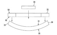
21,25,27,121,122,123…樹脂絶縁層としての第1の樹脂絶縁層
322…樹脂絶縁層及び基準樹脂絶縁層としての第1の樹脂絶縁層
22,23,26,124,222,321…樹脂絶縁層としての第2の樹脂絶縁層
24,221…樹脂絶縁層及び基準樹脂絶縁層としての第2の樹脂絶縁層
28…導体層
29…無機材料及び無機フィラーとしてのガラスフィラー
30,130,230,330…積層構造体としての配線積層部
31…第1主面
32…第2主面
34…ビア導体
41…ICチップ接続端子
45…母基板接続端子
51…補強材としてのスティフナ
61…ICチップ
A1…仮想線と第1主面に属する線分との間の領域(基準樹脂絶縁層の第1主面側の領域)
A2…仮想線と第2主面に属する線分との間の領域(基準樹脂絶縁層の第2主面側の領域)
L…仮想線
L1…第1主面に属する線分
L2…第2主面に属する線分
Claims (1)
- 複数の樹脂絶縁層及び複数の導体層を交互に積層した多層化した積層構造体を有し、前記積層構造体の第1主面側には、接続対象がICチップである複数のICチップ接続端子が配置され、前記積層構造体の第2主面側には、接続対象が母基板である複数の母基板接続端子が配置され、前記複数の導体層は、前記複数の樹脂絶縁層に形成され、いずれも前記第2主面側から前記第1主面側に向かうに従って拡径した形状、または、いずれも前記第1主面側から前記第2主面側に向かうに従って拡径した形状を有するビア導体により接続されている多層配線基板であって、
前記複数の樹脂絶縁層は、樹脂絶縁材料を主体としたビルドアップ材によって形成された第1の樹脂絶縁層と、前記第1の樹脂絶縁層よりも多量の無機材料を含有しかつ前記第1の樹脂絶縁層よりも熱膨張係数が小さいビルドアップ材によって形成された第2の樹脂絶縁層とを含み、
前記第2の樹脂絶縁層は、無機フィラー及び無機繊維クロスの少なくとも一方を前記無機材料として含有しており、
前記第1主面側の最外層の樹脂絶縁層及び前記第2主面側の最外層の樹脂絶縁層の少なくとも一方は、前記第1の樹脂絶縁層であり、
前記積層構造体の厚さ方向における中央に、複数の前記第2の樹脂絶縁層からなる積層体が配置され、前記積層体の前記第1主面側に、前記第1の樹脂絶縁層を介して前記第2の樹脂絶縁層がさらに積層され、
前記積層構造体を厚さ方向に切断した切断面において、前記第1主面との距離及び前記第2主面との距離が互いに等しくなる箇所に設定された仮想線と前記第2主面に属する線分との間の領域に占める前記第2の樹脂絶縁層の厚さの比率が、前記仮想線と前記第1主面に属する線分との間の領域に占める前記第2の樹脂絶縁層の厚さの比率よりも大きくなっており、
前記積層構造体には、前記第2主面側が凸となる反りが生じており、
前記第1主面側に、前記複数のICチップ接続端子を露出させるとともに、平面視で全体として枠状をなす補強材が接合される
ことを特徴とする多層配線基板。
Priority Applications (5)
| Application Number | Priority Date | Filing Date | Title |
|---|---|---|---|
| JP2010173305A JP5079059B2 (ja) | 2010-08-02 | 2010-08-02 | 多層配線基板 |
| TW100126899A TWI461117B (zh) | 2010-08-02 | 2011-07-29 | 多層配線基板 |
| US13/195,290 US8530751B2 (en) | 2010-08-02 | 2011-08-01 | Multilayer wiring substrate |
| KR1020110076655A KR101322126B1 (ko) | 2010-08-02 | 2011-08-01 | 다층 배선기판 |
| CN201110225099.1A CN102347287B (zh) | 2010-08-02 | 2011-08-02 | 多层布线基板 |
Applications Claiming Priority (1)
| Application Number | Priority Date | Filing Date | Title |
|---|---|---|---|
| JP2010173305A JP5079059B2 (ja) | 2010-08-02 | 2010-08-02 | 多層配線基板 |
Related Child Applications (1)
| Application Number | Title | Priority Date | Filing Date |
|---|---|---|---|
| JP2012005848A Division JP5449413B2 (ja) | 2012-01-16 | 2012-01-16 | 多層配線基板 |
Publications (3)
| Publication Number | Publication Date |
|---|---|
| JP2012033790A JP2012033790A (ja) | 2012-02-16 |
| JP2012033790A5 JP2012033790A5 (ja) | 2012-05-10 |
| JP5079059B2 true JP5079059B2 (ja) | 2012-11-21 |
Family
ID=45525552
Family Applications (1)
| Application Number | Title | Priority Date | Filing Date |
|---|---|---|---|
| JP2010173305A Expired - Fee Related JP5079059B2 (ja) | 2010-08-02 | 2010-08-02 | 多層配線基板 |
Country Status (5)
| Country | Link |
|---|---|
| US (1) | US8530751B2 (ja) |
| JP (1) | JP5079059B2 (ja) |
| KR (1) | KR101322126B1 (ja) |
| CN (1) | CN102347287B (ja) |
| TW (1) | TWI461117B (ja) |
Families Citing this family (34)
| Publication number | Priority date | Publication date | Assignee | Title |
|---|---|---|---|---|
| US8780576B2 (en) * | 2011-09-14 | 2014-07-15 | Invensas Corporation | Low CTE interposer |
| KR101939236B1 (ko) * | 2011-11-10 | 2019-01-16 | 삼성전자 주식회사 | 기판 및 이를 포함하는 전자 장치 |
| WO2013095363A1 (en) * | 2011-12-20 | 2013-06-27 | Intel Corporation | Microelectronic package and stacked microelectronic assembly and computing system containing same |
| US9117730B2 (en) * | 2011-12-29 | 2015-08-25 | Ibiden Co., Ltd. | Printed wiring board and method for manufacturing printed wiring board |
| KR101331669B1 (ko) * | 2012-03-08 | 2013-11-20 | 삼성전기주식회사 | 전력 모듈용 기판 |
| JP5955102B2 (ja) * | 2012-05-29 | 2016-07-20 | 京セラ株式会社 | 配線基板およびその製造方法 |
| US9615447B2 (en) * | 2012-07-23 | 2017-04-04 | Zhuhai Advanced Chip Carriers & Electronic Substrate Solutions Technologies Co. Ltd. | Multilayer electronic support structure with integral constructional elements |
| TW201409633A (zh) * | 2012-08-24 | 2014-03-01 | Kinsus Interconnect Tech Corp | 晶片及載板的封裝結構 |
| JP2014063844A (ja) * | 2012-09-20 | 2014-04-10 | Sony Corp | 半導体装置、半導体装置の製造方法及び電子機器 |
| US8802504B1 (en) | 2013-03-14 | 2014-08-12 | Taiwan Semiconductor Manufacturing Company, Ltd. | 3D packages and methods for forming the same |
| US9299649B2 (en) | 2013-02-08 | 2016-03-29 | Taiwan Semiconductor Manufacturing Company, Ltd. | 3D packages and methods for forming the same |
| CN104218016A (zh) * | 2013-06-04 | 2014-12-17 | 宏启胜精密电子(秦皇岛)有限公司 | Ic载板及具有该ic载板的半导体器件 |
| KR102149793B1 (ko) * | 2013-10-24 | 2020-08-31 | 삼성전기주식회사 | 인쇄회로기판 및 인쇄회로기판의 휨 제어방법 |
| WO2016103359A1 (ja) * | 2014-12-24 | 2016-06-30 | ルネサスエレクトロニクス株式会社 | 半導体装置 |
| US20160204056A1 (en) * | 2015-01-14 | 2016-07-14 | Bridge Semiconductor Corporation | Wiring board with interposer and dual wiring structures integrated together and method of making the same |
| TW201626531A (zh) * | 2015-01-14 | 2016-07-16 | 鈺橋半導體股份有限公司 | 中介層嵌置於加強層中之線路板及其製作方法 |
| CN105870075A (zh) * | 2015-01-22 | 2016-08-17 | 恒劲科技股份有限公司 | 基板结构 |
| CN106034374B (zh) * | 2015-03-12 | 2018-10-16 | 日立汽车系统(苏州)有限公司 | 防基板变形结构 |
| TWI603505B (zh) * | 2015-04-07 | 2017-10-21 | 矽品精密工業股份有限公司 | 封裝基板 |
| JP2016219452A (ja) * | 2015-05-14 | 2016-12-22 | 富士通株式会社 | 多層基板及び多層基板の製造方法 |
| JP2016219478A (ja) * | 2015-05-15 | 2016-12-22 | イビデン株式会社 | 配線基板及びその製造方法 |
| US10109588B2 (en) * | 2015-05-15 | 2018-10-23 | Samsung Electro-Mechanics Co., Ltd. | Electronic component package and package-on-package structure including the same |
| JP6819599B2 (ja) * | 2015-09-25 | 2021-01-27 | 大日本印刷株式会社 | 実装部品、配線基板、電子装置、およびその製造方法 |
| KR102512228B1 (ko) * | 2015-10-01 | 2023-03-21 | 삼성전기주식회사 | 절연재 및 이를 포함하는 인쇄회로기판 |
| US9711458B2 (en) * | 2015-11-13 | 2017-07-18 | Taiwan Semiconductor Manufacturing Company, Ltd. | Structure and formation method for chip package |
| KR101912278B1 (ko) | 2015-12-21 | 2018-10-29 | 삼성전기 주식회사 | 전자 부품 패키지 및 그 제조방법 |
| TWI563602B (en) * | 2016-04-15 | 2016-12-21 | Phoenix Pioneer Technology Co Ltd | Method of fabricating a package substrate |
| US9761535B1 (en) * | 2016-06-27 | 2017-09-12 | Nanya Technology Corporation | Interposer, semiconductor package with the same and method for preparing a semiconductor package with the same |
| KR102456322B1 (ko) * | 2017-11-08 | 2022-10-19 | 삼성전기주식회사 | 기판 스트립 및 이를 포함하는 전자소자 패키지 |
| US10242964B1 (en) | 2018-01-16 | 2019-03-26 | Bridge Semiconductor Corp. | Wiring substrate for stackable semiconductor assembly and stackable semiconductor assembly using the same |
| TWI655739B (zh) * | 2018-04-19 | 2019-04-01 | 南亞電路板股份有限公司 | 封裝結構及其形成方法 |
| JP7099359B2 (ja) | 2019-02-20 | 2022-07-12 | 株式会社村田製作所 | コイル部品 |
| US11094649B2 (en) * | 2020-01-21 | 2021-08-17 | Advanced Semiconductor Engineering, Inc. | Semiconductor package structure and method for manufacturing the same |
| US11233035B2 (en) * | 2020-05-28 | 2022-01-25 | Taiwan Semiconductor Manufacturing Company, Ltd. | Package structure and method of manufacturing the same |
Family Cites Families (12)
| Publication number | Priority date | Publication date | Assignee | Title |
|---|---|---|---|---|
| JP2004356569A (ja) | 2003-05-30 | 2004-12-16 | Shinko Electric Ind Co Ltd | 半導体装置用パッケージ |
| JP4342366B2 (ja) * | 2004-04-09 | 2009-10-14 | 日本特殊陶業株式会社 | 配線基板の製造方法 |
| JP2006287056A (ja) * | 2005-04-01 | 2006-10-19 | Ngk Spark Plug Co Ltd | 配線基板および配線基板の製造方法 |
| JP4072176B2 (ja) | 2005-08-29 | 2008-04-09 | 新光電気工業株式会社 | 多層配線基板の製造方法 |
| JP2008078683A (ja) | 2005-08-29 | 2008-04-03 | Shinko Electric Ind Co Ltd | 多層配線基板 |
| JP2008118154A (ja) | 2007-12-20 | 2008-05-22 | Shinko Electric Ind Co Ltd | 半導体装置用パッケージ |
| JP2008118155A (ja) | 2007-12-20 | 2008-05-22 | Shinko Electric Ind Co Ltd | 半導体装置用パッケージ |
| JP5290017B2 (ja) * | 2008-03-28 | 2013-09-18 | 日本特殊陶業株式会社 | 多層配線基板及びその製造方法 |
| JP5179920B2 (ja) * | 2008-03-28 | 2013-04-10 | 日本特殊陶業株式会社 | 多層配線基板 |
| US8129828B2 (en) | 2008-09-29 | 2012-03-06 | Ngk Spark Plug Co., Ltd. | Wiring substrate with reinforcement |
| JP5306789B2 (ja) | 2008-12-03 | 2013-10-02 | 日本特殊陶業株式会社 | 多層配線基板及びその製造方法 |
| JP4473935B1 (ja) | 2009-07-06 | 2010-06-02 | 新光電気工業株式会社 | 多層配線基板 |
-
2010
- 2010-08-02 JP JP2010173305A patent/JP5079059B2/ja not_active Expired - Fee Related
-
2011
- 2011-07-29 TW TW100126899A patent/TWI461117B/zh not_active IP Right Cessation
- 2011-08-01 US US13/195,290 patent/US8530751B2/en not_active Expired - Fee Related
- 2011-08-01 KR KR1020110076655A patent/KR101322126B1/ko not_active IP Right Cessation
- 2011-08-02 CN CN201110225099.1A patent/CN102347287B/zh not_active Expired - Fee Related
Also Published As
| Publication number | Publication date |
|---|---|
| KR20120022593A (ko) | 2012-03-12 |
| CN102347287A (zh) | 2012-02-08 |
| CN102347287B (zh) | 2015-01-28 |
| TW201220980A (en) | 2012-05-16 |
| TWI461117B (zh) | 2014-11-11 |
| US20120024582A1 (en) | 2012-02-02 |
| KR101322126B1 (ko) | 2013-10-28 |
| JP2012033790A (ja) | 2012-02-16 |
| US8530751B2 (en) | 2013-09-10 |
Similar Documents
| Publication | Publication Date | Title |
|---|---|---|
| JP5079059B2 (ja) | 多層配線基板 | |
| JP5284235B2 (ja) | 半導体パッケージ | |
| JP5289996B2 (ja) | 補強材付き配線基板 | |
| JP5356876B2 (ja) | 多層配線基板及びその製造方法 | |
| JP5284147B2 (ja) | 多層配線基板 | |
| JP5290017B2 (ja) | 多層配線基板及びその製造方法 | |
| JP5179920B2 (ja) | 多層配線基板 | |
| JP5902931B2 (ja) | 配線基板の製造方法、及び、配線基板製造用の支持体 | |
| JP5367523B2 (ja) | 配線基板及び配線基板の製造方法 | |
| JP5172404B2 (ja) | 多層配線基板の製造方法、及び多層配線基板の中間製品 | |
| JP2015211194A (ja) | プリント配線板および半導体パッケージ、ならびにプリント配線板の製造方法 | |
| JP5260215B2 (ja) | 補強材付き配線基板の製造方法 | |
| JP5129783B2 (ja) | 補強材付き配線基板及びその製造方法 | |
| JP5306879B2 (ja) | 補強材付き配線基板 | |
| JP5449413B2 (ja) | 多層配線基板 | |
| JP5340622B2 (ja) | 多層配線基板 | |
| JP5350829B2 (ja) | 補強材付き配線基板の製造方法、補強材付き配線基板用の配線基板 | |
| JP5330286B2 (ja) | 補強材付き配線基板の製造方法 | |
| JP2004214271A (ja) | 片面積層配線基板及びその製造方法 | |
| JP5356883B2 (ja) | 補強材付き配線基板の製造方法 | |
| TWI507109B (zh) | A supporting substrate for manufacturing a multilayer wiring board, and a method for manufacturing the multilayer wiring board |
Legal Events
| Date | Code | Title | Description |
|---|---|---|---|
| A621 | Written request for application examination |
Free format text: JAPANESE INTERMEDIATE CODE: A621 Effective date: 20120116 |
|
| A521 | Request for written amendment filed |
Free format text: JAPANESE INTERMEDIATE CODE: A523 Effective date: 20120316 |
|
| A131 | Notification of reasons for refusal |
Free format text: JAPANESE INTERMEDIATE CODE: A131 Effective date: 20120515 |
|
| A977 | Report on retrieval |
Free format text: JAPANESE INTERMEDIATE CODE: A971007 Effective date: 20120517 |
|
| A521 | Request for written amendment filed |
Free format text: JAPANESE INTERMEDIATE CODE: A523 Effective date: 20120709 |
|
| TRDD | Decision of grant or rejection written | ||
| A01 | Written decision to grant a patent or to grant a registration (utility model) |
Free format text: JAPANESE INTERMEDIATE CODE: A01 Effective date: 20120807 |
|
| A01 | Written decision to grant a patent or to grant a registration (utility model) |
Free format text: JAPANESE INTERMEDIATE CODE: A01 |
|
| A61 | First payment of annual fees (during grant procedure) |
Free format text: JAPANESE INTERMEDIATE CODE: A61 Effective date: 20120828 |
|
| FPAY | Renewal fee payment (event date is renewal date of database) |
Free format text: PAYMENT UNTIL: 20150907 Year of fee payment: 3 |
|
| R150 | Certificate of patent or registration of utility model |
Free format text: JAPANESE INTERMEDIATE CODE: R150 |
|
| R250 | Receipt of annual fees |
Free format text: JAPANESE INTERMEDIATE CODE: R250 |
|
| LAPS | Cancellation because of no payment of annual fees |