JP5073097B2 - 電極アセンブリ、基板を処理するための装置および基板を処理するための方法 - Google Patents
電極アセンブリ、基板を処理するための装置および基板を処理するための方法 Download PDFInfo
- Publication number
- JP5073097B2 JP5073097B2 JP2011507519A JP2011507519A JP5073097B2 JP 5073097 B2 JP5073097 B2 JP 5073097B2 JP 2011507519 A JP2011507519 A JP 2011507519A JP 2011507519 A JP2011507519 A JP 2011507519A JP 5073097 B2 JP5073097 B2 JP 5073097B2
- Authority
- JP
- Japan
- Prior art keywords
- substrate
- recess
- conductive faceplate
- plasma
- slope
- Prior art date
- Legal status (The legal status is an assumption and is not a legal conclusion. Google has not performed a legal analysis and makes no representation as to the accuracy of the status listed.)
- Expired - Fee Related
Links
Images
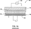

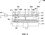


Classifications
-
- C—CHEMISTRY; METALLURGY
- C23—COATING METALLIC MATERIAL; COATING MATERIAL WITH METALLIC MATERIAL; CHEMICAL SURFACE TREATMENT; DIFFUSION TREATMENT OF METALLIC MATERIAL; COATING BY VACUUM EVAPORATION, BY SPUTTERING, BY ION IMPLANTATION OR BY CHEMICAL VAPOUR DEPOSITION, IN GENERAL; INHIBITING CORROSION OF METALLIC MATERIAL OR INCRUSTATION IN GENERAL
- C23C—COATING METALLIC MATERIAL; COATING MATERIAL WITH METALLIC MATERIAL; SURFACE TREATMENT OF METALLIC MATERIAL BY DIFFUSION INTO THE SURFACE, BY CHEMICAL CONVERSION OR SUBSTITUTION; COATING BY VACUUM EVAPORATION, BY SPUTTERING, BY ION IMPLANTATION OR BY CHEMICAL VAPOUR DEPOSITION, IN GENERAL
- C23C16/00—Chemical coating by decomposition of gaseous compounds, without leaving reaction products of surface material in the coating, i.e. chemical vapour deposition [CVD] processes
- C23C16/44—Chemical coating by decomposition of gaseous compounds, without leaving reaction products of surface material in the coating, i.e. chemical vapour deposition [CVD] processes characterised by the method of coating
- C23C16/50—Chemical coating by decomposition of gaseous compounds, without leaving reaction products of surface material in the coating, i.e. chemical vapour deposition [CVD] processes characterised by the method of coating using electric discharges
- C23C16/505—Chemical coating by decomposition of gaseous compounds, without leaving reaction products of surface material in the coating, i.e. chemical vapour deposition [CVD] processes characterised by the method of coating using electric discharges using radio frequency discharges
- C23C16/509—Chemical coating by decomposition of gaseous compounds, without leaving reaction products of surface material in the coating, i.e. chemical vapour deposition [CVD] processes characterised by the method of coating using electric discharges using radio frequency discharges using internal electrodes
- C23C16/5096—Flat-bed apparatus
-
- H—ELECTRICITY
- H01—ELECTRIC ELEMENTS
- H01J—ELECTRIC DISCHARGE TUBES OR DISCHARGE LAMPS
- H01J37/00—Discharge tubes with provision for introducing objects or material to be exposed to the discharge, e.g. for the purpose of examination or processing thereof
- H01J37/32—Gas-filled discharge tubes
- H01J37/32431—Constructional details of the reactor
- H01J37/3244—Gas supply means
-
- H—ELECTRICITY
- H01—ELECTRIC ELEMENTS
- H01J—ELECTRIC DISCHARGE TUBES OR DISCHARGE LAMPS
- H01J37/00—Discharge tubes with provision for introducing objects or material to be exposed to the discharge, e.g. for the purpose of examination or processing thereof
- H01J37/32—Gas-filled discharge tubes
- H01J37/32431—Constructional details of the reactor
- H01J37/32532—Electrodes
- H01J37/32541—Shape
-
- Y—GENERAL TAGGING OF NEW TECHNOLOGICAL DEVELOPMENTS; GENERAL TAGGING OF CROSS-SECTIONAL TECHNOLOGIES SPANNING OVER SEVERAL SECTIONS OF THE IPC; TECHNICAL SUBJECTS COVERED BY FORMER USPC CROSS-REFERENCE ART COLLECTIONS [XRACs] AND DIGESTS
- Y10—TECHNICAL SUBJECTS COVERED BY FORMER USPC
- Y10T—TECHNICAL SUBJECTS COVERED BY FORMER US CLASSIFICATION
- Y10T117/00—Single-crystal, oriented-crystal, and epitaxy growth processes; non-coating apparatus therefor
- Y10T117/10—Apparatus
Landscapes
- Chemical & Material Sciences (AREA)
- Engineering & Computer Science (AREA)
- Physics & Mathematics (AREA)
- Plasma & Fusion (AREA)
- Analytical Chemistry (AREA)
- Materials Engineering (AREA)
- Chemical Kinetics & Catalysis (AREA)
- Mechanical Engineering (AREA)
- Metallurgy (AREA)
- Organic Chemistry (AREA)
- General Chemical & Material Sciences (AREA)
- Chemical Vapour Deposition (AREA)
- Drying Of Semiconductors (AREA)
- Plasma Technology (AREA)
- Gas-Filled Discharge Tubes (AREA)
Applications Claiming Priority (3)
| Application Number | Priority Date | Filing Date | Title |
|---|---|---|---|
| US12/110,879 | 2008-04-28 | ||
| US12/110,879 US8097082B2 (en) | 2008-04-28 | 2008-04-28 | Nonplanar faceplate for a plasma processing chamber |
| PCT/US2009/039674 WO2009134588A2 (en) | 2008-04-28 | 2009-04-06 | Nonplanar faceplate for a plasma processing chamber |
Publications (3)
| Publication Number | Publication Date |
|---|---|
| JP2011518959A JP2011518959A (ja) | 2011-06-30 |
| JP2011518959A5 JP2011518959A5 (cg-RX-API-DMAC10.html) | 2012-07-19 |
| JP5073097B2 true JP5073097B2 (ja) | 2012-11-14 |
Family
ID=41215290
Family Applications (1)
| Application Number | Title | Priority Date | Filing Date |
|---|---|---|---|
| JP2011507519A Expired - Fee Related JP5073097B2 (ja) | 2008-04-28 | 2009-04-06 | 電極アセンブリ、基板を処理するための装置および基板を処理するための方法 |
Country Status (6)
| Country | Link |
|---|---|
| US (1) | US8097082B2 (cg-RX-API-DMAC10.html) |
| JP (1) | JP5073097B2 (cg-RX-API-DMAC10.html) |
| KR (1) | KR20100135967A (cg-RX-API-DMAC10.html) |
| CN (1) | CN102017813A (cg-RX-API-DMAC10.html) |
| TW (1) | TWI395517B (cg-RX-API-DMAC10.html) |
| WO (1) | WO2009134588A2 (cg-RX-API-DMAC10.html) |
Families Citing this family (16)
| Publication number | Priority date | Publication date | Assignee | Title |
|---|---|---|---|---|
| US7413612B2 (en) * | 2003-07-10 | 2008-08-19 | Applied Materials, Inc. | In situ substrate holder leveling method and apparatus |
| US7572340B2 (en) * | 2004-11-29 | 2009-08-11 | Applied Materials, Inc. | High resolution substrate holder leveling device and method |
| US10100408B2 (en) | 2014-03-03 | 2018-10-16 | Applied Materials, Inc. | Edge hump reduction faceplate by plasma modulation |
| KR102122113B1 (ko) * | 2014-10-17 | 2020-06-29 | 램 리써치 코포레이션 | 튜닝가능한 가스 흐름 제어를 위한 가스 스플리터를 포함하는 가스 공급 전달 장치 |
| CN107937886A (zh) * | 2017-11-14 | 2018-04-20 | 武汉华星光电半导体显示技术有限公司 | 化学气相沉积设备及成膜方法 |
| KR102162379B1 (ko) * | 2018-01-24 | 2020-10-06 | 어플라이드 머티어리얼스, 인코포레이티드 | 가열식 세라믹 면판 |
| US20190244793A1 (en) * | 2018-02-05 | 2019-08-08 | Lam Research Corporation | Tapered upper electrode for uniformity control in plasma processing |
| WO2020247269A1 (en) * | 2019-06-07 | 2020-12-10 | Applied Materials, Inc. | Faceplate having a curved surface |
| US11236424B2 (en) * | 2019-11-01 | 2022-02-01 | Applied Materials, Inc. | Process kit for improving edge film thickness uniformity on a substrate |
| US12654181B2 (en) | 2020-01-29 | 2026-06-16 | Lam Research Corporation | Gas distribution faceplate with oblique flow paths |
| US20210287881A1 (en) * | 2020-03-12 | 2021-09-16 | Applied Materials, Inc. | Methods and apparatus for tuning semiconductor processes |
| CN111370287B (zh) * | 2020-03-24 | 2025-06-10 | 长江存储科技有限责任公司 | 一种上电极设备以及等离子体处理装置 |
| CN114075660B (zh) * | 2020-08-14 | 2022-09-27 | 长鑫存储技术有限公司 | 喷淋头、化学气相沉积设备及其工作方法 |
| KR102793905B1 (ko) | 2020-08-14 | 2025-04-08 | 삼성전자주식회사 | 상부 전극 및 이를 포함하는 기판 처리 장치 |
| US12338530B2 (en) | 2021-07-09 | 2025-06-24 | Applied Materials, Inc. | Shaped showerhead for edge plasma modulation |
| US20250029849A1 (en) * | 2023-07-18 | 2025-01-23 | Applied Materials, Inc. | Shaped faceplate for extreme edge film uniformity |
Family Cites Families (59)
| Publication number | Priority date | Publication date | Assignee | Title |
|---|---|---|---|---|
| US650253A (en) * | 1899-11-23 | 1900-05-22 | Henry Keller | Thresher. |
| US3830194A (en) * | 1972-09-28 | 1974-08-20 | Applied Materials Tech | Susceptor support structure and docking assembly |
| US4455467A (en) * | 1981-09-21 | 1984-06-19 | General Electric Company | Metal rack for microwave oven |
| US4522149A (en) * | 1983-11-21 | 1985-06-11 | General Instrument Corp. | Reactor and susceptor for chemical vapor deposition process |
| US4809421A (en) * | 1984-01-16 | 1989-03-07 | Precision Brand Products, Inc. | Slotted shim |
| US5000113A (en) * | 1986-12-19 | 1991-03-19 | Applied Materials, Inc. | Thermal CVD/PECVD reactor and use for thermal chemical vapor deposition of silicon dioxide and in-situ multi-step planarized process |
| JPS644481A (en) * | 1987-06-24 | 1989-01-09 | Minoru Sugawara | Parallel-plate discharge electrode |
| US4927991A (en) * | 1987-11-10 | 1990-05-22 | The Pillsbury Company | Susceptor in combination with grid for microwave oven package |
| US5044943A (en) * | 1990-08-16 | 1991-09-03 | Applied Materials, Inc. | Spoked susceptor support for enhanced thermal uniformity of susceptor in semiconductor wafer processing apparatus |
| US5173580A (en) * | 1990-11-15 | 1992-12-22 | The Pillsbury Company | Susceptor with conductive border for heating foods in a microwave oven |
| US5820686A (en) * | 1993-01-21 | 1998-10-13 | Moore Epitaxial, Inc. | Multi-layer susceptor for rapid thermal process reactors |
| US5352294A (en) * | 1993-01-28 | 1994-10-04 | White John M | Alignment of a shadow frame and large flat substrates on a support |
| JP2662365B2 (ja) * | 1993-01-28 | 1997-10-08 | アプライド マテリアルズ インコーポレイテッド | 改良された排出システムを有する単一基板式の真空処理装置 |
| US5421893A (en) * | 1993-02-26 | 1995-06-06 | Applied Materials, Inc. | Susceptor drive and wafer displacement mechanism |
| US5439524A (en) * | 1993-04-05 | 1995-08-08 | Vlsi Technology, Inc. | Plasma processing apparatus |
| US5332443A (en) * | 1993-06-09 | 1994-07-26 | Applied Materials, Inc. | Lift fingers for substrate processing apparatus |
| US5614055A (en) * | 1993-08-27 | 1997-03-25 | Applied Materials, Inc. | High density plasma CVD and etching reactor |
| US5628869A (en) * | 1994-05-09 | 1997-05-13 | Lsi Logic Corporation | Plasma enhanced chemical vapor reactor with shaped electrodes |
| WO1997009737A1 (en) * | 1995-09-01 | 1997-03-13 | Advanced Semiconductor Materials America, Inc. | Wafer support system |
| JPH09306896A (ja) * | 1996-03-15 | 1997-11-28 | Sumitomo Metal Ind Ltd | プラズマ処理装置およびプラズマ処理方法 |
| US5844205A (en) * | 1996-04-19 | 1998-12-01 | Applied Komatsu Technology, Inc. | Heated substrate support structure |
| US5819434A (en) * | 1996-04-25 | 1998-10-13 | Applied Materials, Inc. | Etch enhancement using an improved gas distribution plate |
| KR100252210B1 (ko) * | 1996-12-24 | 2000-04-15 | 윤종용 | 반도체장치 제조용 건식식각장치 |
| US5981899A (en) * | 1997-01-17 | 1999-11-09 | Balzers Aktiengesellschaft | Capacitively coupled RF-plasma reactor |
| JP4906169B2 (ja) * | 1997-06-13 | 2012-03-28 | エリコン・トレーディング・アクチェンゲゼルシャフト,トリュープバッハ | 被覆工作物を製造するための方法、その方法の利用およびそのための装置 |
| US20020011215A1 (en) * | 1997-12-12 | 2002-01-31 | Goushu Tei | Plasma treatment apparatus and method of manufacturing optical parts using the same |
| KR100279963B1 (ko) * | 1997-12-30 | 2001-04-02 | 윤종용 | 반도체소자제조용가스디퓨져및이를설치한반응로 |
| AU2186099A (en) * | 1998-02-09 | 1999-08-23 | Nikon Corporation | Apparatus for supporting base plate, apparatus and method for transferring base plate, method of replacing base plate, and exposure apparatus and method of manufacturing the same |
| GB9808825D0 (en) * | 1998-04-24 | 1998-06-24 | Nimbus Communications Int Ltd | A disk recording system and a method of controlling the rotation of a turntable in such a disk recording system |
| US6182603B1 (en) * | 1998-07-13 | 2001-02-06 | Applied Komatsu Technology, Inc. | Surface-treated shower head for use in a substrate processing chamber |
| US6619131B2 (en) * | 1998-07-16 | 2003-09-16 | Unaxis Balzers Ag | Combination pressure sensor with capacitive and thermal elements |
| JP5031944B2 (ja) * | 1998-09-30 | 2012-09-26 | オー・ツェー・エリコン・バルザース・アクチェンゲゼルシャフト | 真空処理装置および表面処理方法 |
| TW469534B (en) * | 1999-02-23 | 2001-12-21 | Matsushita Electric Industrial Co Ltd | Plasma processing method and apparatus |
| JP3417328B2 (ja) * | 1999-02-23 | 2003-06-16 | 松下電器産業株式会社 | プラズマ処理方法及び装置 |
| US6344420B1 (en) * | 1999-03-15 | 2002-02-05 | Kabushiki Kaisha Toshiba | Plasma processing method and plasma processing apparatus |
| JP3595853B2 (ja) * | 1999-03-18 | 2004-12-02 | 日本エー・エス・エム株式会社 | プラズマcvd成膜装置 |
| US6228438B1 (en) * | 1999-08-10 | 2001-05-08 | Unakis Balzers Aktiengesellschaft | Plasma reactor for the treatment of large size substrates |
| US6149365A (en) * | 1999-09-21 | 2000-11-21 | Applied Komatsu Technology, Inc. | Support frame for substrates |
| US6961490B2 (en) * | 2000-01-27 | 2005-11-01 | Unaxis-Balzers Aktiengesellschaft | Waveguide plate and process for its production and microtitre plate |
| US6510263B1 (en) * | 2000-01-27 | 2003-01-21 | Unaxis Balzers Aktiengesellschaft | Waveguide plate and process for its production and microtitre plate |
| US6900596B2 (en) * | 2002-07-09 | 2005-05-31 | Applied Materials, Inc. | Capacitively coupled plasma reactor with uniform radial distribution of plasma |
| US6502530B1 (en) | 2000-04-26 | 2003-01-07 | Unaxis Balzers Aktiengesellschaft | Design of gas injection for the electrode in a capacitively coupled RF plasma reactor |
| US6383573B1 (en) * | 2000-05-17 | 2002-05-07 | Unaxis Balzers Aktiengesellschaft | Process for manufacturing coated plastic body |
| KR100332314B1 (ko) * | 2000-06-24 | 2002-04-12 | 서성기 | 박막증착용 반응용기 |
| US6447980B1 (en) * | 2000-07-19 | 2002-09-10 | Clariant Finance (Bvi) Limited | Photoresist composition for deep UV and process thereof |
| WO2002042518A1 (de) * | 2000-11-27 | 2002-05-30 | Unaxis Trading Ag | Target mit dickenprofilierung für rf manetron |
| US6962732B2 (en) * | 2001-08-23 | 2005-11-08 | Applied Materials, Inc. | Process for controlling thin film uniformity and products produced thereby |
| US6793733B2 (en) * | 2002-01-25 | 2004-09-21 | Applied Materials Inc. | Gas distribution showerhead |
| JP3872363B2 (ja) * | 2002-03-12 | 2007-01-24 | 京セラ株式会社 | Cat−PECVD法 |
| JP4044368B2 (ja) * | 2002-05-22 | 2008-02-06 | 松下電器産業株式会社 | プラズマ処理方法及び装置 |
| US7270713B2 (en) * | 2003-01-07 | 2007-09-18 | Applied Materials, Inc. | Tunable gas distribution plate assembly |
| US7083702B2 (en) * | 2003-06-12 | 2006-08-01 | Applied Materials, Inc. | RF current return path for a large area substrate plasma reactor |
| JP4563729B2 (ja) * | 2003-09-04 | 2010-10-13 | 東京エレクトロン株式会社 | プラズマ処理装置 |
| ES2287755T3 (es) * | 2003-09-10 | 2007-12-16 | Oc Oerlikon Balzers Ag | Metodo de compensacion de falta de uniformidad de tension para un reactor de plasma de alta frecuencia para el tratamiento de sustratos de gran area rectangular. |
| US8074599B2 (en) * | 2004-05-12 | 2011-12-13 | Applied Materials, Inc. | Plasma uniformity control by gas diffuser curvature |
| US20060005771A1 (en) * | 2004-07-12 | 2006-01-12 | Applied Materials, Inc. | Apparatus and method of shaping profiles of large-area PECVD electrodes |
| US7429410B2 (en) * | 2004-09-20 | 2008-09-30 | Applied Materials, Inc. | Diffuser gravity support |
| KR20070089533A (ko) | 2006-02-28 | 2007-08-31 | 삼성전자주식회사 | 플라즈마 처리설비 |
| JP2011071544A (ja) * | 2010-12-06 | 2011-04-07 | Ulvac Japan Ltd | プラズマ処理方法及び装置並びにプラズマcvd方法及び装置 |
-
2008
- 2008-04-28 US US12/110,879 patent/US8097082B2/en not_active Expired - Fee Related
-
2009
- 2009-04-06 KR KR1020107026833A patent/KR20100135967A/ko not_active Ceased
- 2009-04-06 CN CN200980115050.1A patent/CN102017813A/zh active Pending
- 2009-04-06 JP JP2011507519A patent/JP5073097B2/ja not_active Expired - Fee Related
- 2009-04-06 WO PCT/US2009/039674 patent/WO2009134588A2/en not_active Ceased
- 2009-04-28 TW TW098114076A patent/TWI395517B/zh not_active IP Right Cessation
Also Published As
| Publication number | Publication date |
|---|---|
| TWI395517B (zh) | 2013-05-01 |
| WO2009134588A2 (en) | 2009-11-05 |
| TW201008398A (en) | 2010-02-16 |
| KR20100135967A (ko) | 2010-12-27 |
| US20090269512A1 (en) | 2009-10-29 |
| JP2011518959A (ja) | 2011-06-30 |
| WO2009134588A3 (en) | 2010-03-18 |
| US8097082B2 (en) | 2012-01-17 |
| CN102017813A (zh) | 2011-04-13 |
Similar Documents
| Publication | Publication Date | Title |
|---|---|---|
| US8097082B2 (en) | Nonplanar faceplate for a plasma processing chamber | |
| US12198966B2 (en) | Substrate support with multiple embedded electrodes | |
| US8636871B2 (en) | Plasma processing apparatus, plasma processing method and storage medium | |
| TWI574345B (zh) | 靜電夾盤 | |
| KR101451244B1 (ko) | 라이너 어셈블리 및 이를 구비하는 기판 처리 장치 | |
| US8869742B2 (en) | Plasma processing chamber with dual axial gas injection and exhaust | |
| CN102150243B (zh) | 温控热边缘环组合件 | |
| US20090165722A1 (en) | Apparatus for treating substrate | |
| US20140138030A1 (en) | Capacitively coupled plasma equipment with uniform plasma density | |
| US20090017635A1 (en) | Apparatus and method for processing a substrate edge region | |
| US20140141619A1 (en) | Capacitively coupled plasma equipment with uniform plasma density | |
| TW201522696A (zh) | 使用遠端電漿cvd技術的低溫氮化矽膜 | |
| KR20120080544A (ko) | 포커스 링 및 이 포커스 링을 구비하는 기판 처리 장치 | |
| JP2026020182A (ja) | 温度の影響を受けやすいプロセスのための改善された熱的結合を有する静電チャック | |
| WO2014172112A1 (en) | Capacitively coupled plasma equipment with uniform plasma density | |
| TWI774308B (zh) | 用於高頻處理的蓋堆疊 | |
| CN104046961A (zh) | 衬底支撑器以及包含所述衬底支撑器的衬底处理设备 | |
| JP6068849B2 (ja) | 上部電極、及びプラズマ処理装置 | |
| US20170211185A1 (en) | Ceramic showerhead with embedded conductive layers | |
| KR20200059570A (ko) | 정전 척, 및 그를 포함하는 플라즈마 처리 장치 | |
| KR101614032B1 (ko) | 가스 분배 장치 및 이를 구비하는 기판 처리 장치 | |
| TW202137297A (zh) | 腔室沉積及蝕刻處理 | |
| TW202449948A (zh) | 具有先進遠邊緣電極、靜電夾盤和嵌入式接地電極的高溫可偏壓加熱器 | |
| KR20150034435A (ko) | 기판 처리 장치 | |
| KR101171988B1 (ko) | 플라즈마 처리장치 |
Legal Events
| Date | Code | Title | Description |
|---|---|---|---|
| A621 | Written request for application examination |
Free format text: JAPANESE INTERMEDIATE CODE: A621 Effective date: 20120406 |
|
| A521 | Request for written amendment filed |
Free format text: JAPANESE INTERMEDIATE CODE: A523 Effective date: 20120601 |
|
| A871 | Explanation of circumstances concerning accelerated examination |
Free format text: JAPANESE INTERMEDIATE CODE: A871 Effective date: 20120601 |
|
| A975 | Report on accelerated examination |
Free format text: JAPANESE INTERMEDIATE CODE: A971005 Effective date: 20120626 |
|
| TRDD | Decision of grant or rejection written | ||
| A01 | Written decision to grant a patent or to grant a registration (utility model) |
Free format text: JAPANESE INTERMEDIATE CODE: A01 Effective date: 20120724 |
|
| A01 | Written decision to grant a patent or to grant a registration (utility model) |
Free format text: JAPANESE INTERMEDIATE CODE: A01 |
|
| A61 | First payment of annual fees (during grant procedure) |
Free format text: JAPANESE INTERMEDIATE CODE: A61 Effective date: 20120821 |
|
| R150 | Certificate of patent or registration of utility model |
Ref document number: 5073097 Country of ref document: JP Free format text: JAPANESE INTERMEDIATE CODE: R150 Free format text: JAPANESE INTERMEDIATE CODE: R150 |
|
| FPAY | Renewal fee payment (event date is renewal date of database) |
Free format text: PAYMENT UNTIL: 20150831 Year of fee payment: 3 |
|
| R250 | Receipt of annual fees |
Free format text: JAPANESE INTERMEDIATE CODE: R250 |
|
| R250 | Receipt of annual fees |
Free format text: JAPANESE INTERMEDIATE CODE: R250 |
|
| R250 | Receipt of annual fees |
Free format text: JAPANESE INTERMEDIATE CODE: R250 |
|
| R250 | Receipt of annual fees |
Free format text: JAPANESE INTERMEDIATE CODE: R250 |
|
| R250 | Receipt of annual fees |
Free format text: JAPANESE INTERMEDIATE CODE: R250 |
|
| R250 | Receipt of annual fees |
Free format text: JAPANESE INTERMEDIATE CODE: R250 |
|
| LAPS | Cancellation because of no payment of annual fees |