JP5058505B2 - 表示装置 - Google Patents
表示装置 Download PDFInfo
- Publication number
- JP5058505B2 JP5058505B2 JP2006098011A JP2006098011A JP5058505B2 JP 5058505 B2 JP5058505 B2 JP 5058505B2 JP 2006098011 A JP2006098011 A JP 2006098011A JP 2006098011 A JP2006098011 A JP 2006098011A JP 5058505 B2 JP5058505 B2 JP 5058505B2
- Authority
- JP
- Japan
- Prior art keywords
- light emission
- period
- row
- signal
- current
- Prior art date
- Legal status (The legal status is an assumption and is not a legal conclusion. Google has not performed a legal analysis and makes no representation as to the accuracy of the status listed.)
- Expired - Fee Related
Links
Images


Classifications
-
- G—PHYSICS
- G09—EDUCATION; CRYPTOGRAPHY; DISPLAY; ADVERTISING; SEALS
- G09G—ARRANGEMENTS OR CIRCUITS FOR CONTROL OF INDICATING DEVICES USING STATIC MEANS TO PRESENT VARIABLE INFORMATION
- G09G3/00—Control arrangements or circuits, of interest only in connection with visual indicators other than cathode-ray tubes
- G09G3/20—Control arrangements or circuits, of interest only in connection with visual indicators other than cathode-ray tubes for presentation of an assembly of a number of characters, e.g. a page, by composing the assembly by combination of individual elements arranged in a matrix no fixed position being assigned to or needed to be assigned to the individual characters or partial characters
- G09G3/22—Control arrangements or circuits, of interest only in connection with visual indicators other than cathode-ray tubes for presentation of an assembly of a number of characters, e.g. a page, by composing the assembly by combination of individual elements arranged in a matrix no fixed position being assigned to or needed to be assigned to the individual characters or partial characters using controlled light sources
- G09G3/30—Control arrangements or circuits, of interest only in connection with visual indicators other than cathode-ray tubes for presentation of an assembly of a number of characters, e.g. a page, by composing the assembly by combination of individual elements arranged in a matrix no fixed position being assigned to or needed to be assigned to the individual characters or partial characters using controlled light sources using electroluminescent panels
- G09G3/32—Control arrangements or circuits, of interest only in connection with visual indicators other than cathode-ray tubes for presentation of an assembly of a number of characters, e.g. a page, by composing the assembly by combination of individual elements arranged in a matrix no fixed position being assigned to or needed to be assigned to the individual characters or partial characters using controlled light sources using electroluminescent panels semiconductive, e.g. using light-emitting diodes [LED]
- G09G3/3208—Control arrangements or circuits, of interest only in connection with visual indicators other than cathode-ray tubes for presentation of an assembly of a number of characters, e.g. a page, by composing the assembly by combination of individual elements arranged in a matrix no fixed position being assigned to or needed to be assigned to the individual characters or partial characters using controlled light sources using electroluminescent panels semiconductive, e.g. using light-emitting diodes [LED] organic, e.g. using organic light-emitting diodes [OLED]
- G09G3/3225—Control arrangements or circuits, of interest only in connection with visual indicators other than cathode-ray tubes for presentation of an assembly of a number of characters, e.g. a page, by composing the assembly by combination of individual elements arranged in a matrix no fixed position being assigned to or needed to be assigned to the individual characters or partial characters using controlled light sources using electroluminescent panels semiconductive, e.g. using light-emitting diodes [LED] organic, e.g. using organic light-emitting diodes [OLED] using an active matrix
- G09G3/3233—Control arrangements or circuits, of interest only in connection with visual indicators other than cathode-ray tubes for presentation of an assembly of a number of characters, e.g. a page, by composing the assembly by combination of individual elements arranged in a matrix no fixed position being assigned to or needed to be assigned to the individual characters or partial characters using controlled light sources using electroluminescent panels semiconductive, e.g. using light-emitting diodes [LED] organic, e.g. using organic light-emitting diodes [OLED] using an active matrix with pixel circuitry controlling the current through the light-emitting element
-
- G—PHYSICS
- G09—EDUCATION; CRYPTOGRAPHY; DISPLAY; ADVERTISING; SEALS
- G09G—ARRANGEMENTS OR CIRCUITS FOR CONTROL OF INDICATING DEVICES USING STATIC MEANS TO PRESENT VARIABLE INFORMATION
- G09G3/00—Control arrangements or circuits, of interest only in connection with visual indicators other than cathode-ray tubes
- G09G3/20—Control arrangements or circuits, of interest only in connection with visual indicators other than cathode-ray tubes for presentation of an assembly of a number of characters, e.g. a page, by composing the assembly by combination of individual elements arranged in a matrix no fixed position being assigned to or needed to be assigned to the individual characters or partial characters
- G09G3/22—Control arrangements or circuits, of interest only in connection with visual indicators other than cathode-ray tubes for presentation of an assembly of a number of characters, e.g. a page, by composing the assembly by combination of individual elements arranged in a matrix no fixed position being assigned to or needed to be assigned to the individual characters or partial characters using controlled light sources
- G09G3/30—Control arrangements or circuits, of interest only in connection with visual indicators other than cathode-ray tubes for presentation of an assembly of a number of characters, e.g. a page, by composing the assembly by combination of individual elements arranged in a matrix no fixed position being assigned to or needed to be assigned to the individual characters or partial characters using controlled light sources using electroluminescent panels
- G09G3/32—Control arrangements or circuits, of interest only in connection with visual indicators other than cathode-ray tubes for presentation of an assembly of a number of characters, e.g. a page, by composing the assembly by combination of individual elements arranged in a matrix no fixed position being assigned to or needed to be assigned to the individual characters or partial characters using controlled light sources using electroluminescent panels semiconductive, e.g. using light-emitting diodes [LED]
- G09G3/3208—Control arrangements or circuits, of interest only in connection with visual indicators other than cathode-ray tubes for presentation of an assembly of a number of characters, e.g. a page, by composing the assembly by combination of individual elements arranged in a matrix no fixed position being assigned to or needed to be assigned to the individual characters or partial characters using controlled light sources using electroluminescent panels semiconductive, e.g. using light-emitting diodes [LED] organic, e.g. using organic light-emitting diodes [OLED]
- G09G3/3266—Details of drivers for scan electrodes
-
- G—PHYSICS
- G09—EDUCATION; CRYPTOGRAPHY; DISPLAY; ADVERTISING; SEALS
- G09G—ARRANGEMENTS OR CIRCUITS FOR CONTROL OF INDICATING DEVICES USING STATIC MEANS TO PRESENT VARIABLE INFORMATION
- G09G2300/00—Aspects of the constitution of display devices
- G09G2300/08—Active matrix structure, i.e. with use of active elements, inclusive of non-linear two terminal elements, in the pixels together with light emitting or modulating elements
- G09G2300/0809—Several active elements per pixel in active matrix panels
- G09G2300/0842—Several active elements per pixel in active matrix panels forming a memory circuit, e.g. a dynamic memory with one capacitor
- G09G2300/0861—Several active elements per pixel in active matrix panels forming a memory circuit, e.g. a dynamic memory with one capacitor with additional control of the display period without amending the charge stored in a pixel memory, e.g. by means of additional select electrodes
-
- G—PHYSICS
- G09—EDUCATION; CRYPTOGRAPHY; DISPLAY; ADVERTISING; SEALS
- G09G—ARRANGEMENTS OR CIRCUITS FOR CONTROL OF INDICATING DEVICES USING STATIC MEANS TO PRESENT VARIABLE INFORMATION
- G09G2310/00—Command of the display device
- G09G2310/02—Addressing, scanning or driving the display screen or processing steps related thereto
- G09G2310/0202—Addressing of scan or signal lines
- G09G2310/0205—Simultaneous scanning of several lines in flat panels
-
- G—PHYSICS
- G09—EDUCATION; CRYPTOGRAPHY; DISPLAY; ADVERTISING; SEALS
- G09G—ARRANGEMENTS OR CIRCUITS FOR CONTROL OF INDICATING DEVICES USING STATIC MEANS TO PRESENT VARIABLE INFORMATION
- G09G2310/00—Command of the display device
- G09G2310/02—Addressing, scanning or driving the display screen or processing steps related thereto
- G09G2310/0224—Details of interlacing
-
- G—PHYSICS
- G09—EDUCATION; CRYPTOGRAPHY; DISPLAY; ADVERTISING; SEALS
- G09G—ARRANGEMENTS OR CIRCUITS FOR CONTROL OF INDICATING DEVICES USING STATIC MEANS TO PRESENT VARIABLE INFORMATION
- G09G2320/00—Control of display operating conditions
- G09G2320/02—Improving the quality of display appearance
- G09G2320/0247—Flicker reduction other than flicker reduction circuits used for single beam cathode-ray tubes
-
- G—PHYSICS
- G09—EDUCATION; CRYPTOGRAPHY; DISPLAY; ADVERTISING; SEALS
- G09G—ARRANGEMENTS OR CIRCUITS FOR CONTROL OF INDICATING DEVICES USING STATIC MEANS TO PRESENT VARIABLE INFORMATION
- G09G3/00—Control arrangements or circuits, of interest only in connection with visual indicators other than cathode-ray tubes
- G09G3/20—Control arrangements or circuits, of interest only in connection with visual indicators other than cathode-ray tubes for presentation of an assembly of a number of characters, e.g. a page, by composing the assembly by combination of individual elements arranged in a matrix no fixed position being assigned to or needed to be assigned to the individual characters or partial characters
- G09G3/2007—Display of intermediate tones
- G09G3/2014—Display of intermediate tones by modulation of the duration of a single pulse during which the logic level remains constant
Landscapes
- Engineering & Computer Science (AREA)
- Physics & Mathematics (AREA)
- Computer Hardware Design (AREA)
- General Physics & Mathematics (AREA)
- Theoretical Computer Science (AREA)
- Control Of Indicators Other Than Cathode Ray Tubes (AREA)
- Control Of El Displays (AREA)
- Electroluminescent Light Sources (AREA)
Description
電流に応じて発光輝度が制御される表示素子と、
電流の値が設定され、設定された電流を前記表示素子に供給する画素回路と、
前記表示素子と前記画素回路の組が行方向および列方向にマトリクス状に複数配置された画像表示部と、
前記画像表示部の行毎に設けられた走査線と、
前記画像表示部の行毎に設けられた発光期間制御線と、
前記画像表示部の行数に応じて配置され、前記画素回路が前記表示素子に供給する電流を設定する期間を制御する走査信号を前記走査線に出力し、かつ前記画素回路が前記表示素子に電流を供給する期間を制御する発光期間制御信号を前記発光期間制御線に出力する行制御回路と、
前記画像表示部の列毎に設けられたデータ線と、
前記画像表示部の列数に応じて配置され、前記画素回路が前記表示素子に供給する電流に応じたデータ信号を前記データ線に出力する列制御回路と、
を有する表示装置であって、
1フレームが、
前記行制御回路が前記画像表示部の奇数行の前記走査線に順次前記走査信号を出力し、前記列制御回路が前記データ信号を前記データ線に出力して、前記画像表示部の奇数行の表示素子に供給する電流を当該表示素子の前記画素回路に順次設定する第1の期間と、前記行制御回路が前記画像表示部の偶数行の前記走査線に順次前記走査信号を出力し、前記列制御回路が前記データ信号を前記データ線に出力して、前記画像表示部の偶数行の表示素子に供給する電流を当該表示素子の前記画素回路に順次設定する第2の期間と、からなり、
前記行制御回路が、前記走査信号が出力されている行の前記走査信号が出力されている期間を除き、前記画像表示部の奇数行および偶数行の前記発光期間制御線に、発光期間制御信号を出力して、前記第1の期間および前記第2の期間に、前記表示素子に、当該表示素子の前記画素回路内に設定された電流を複数回に分けて一定期間供給し、
前記発光期間制御信号の発光期間を決めるパルス幅および間隔は一様であって、かつ、前記発光期間制御信号の1周期は前記走査信号が出力されている期間と等しいことを特徴とする。
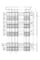
図1において、画像表示部には、RGB原色数のEL素子と、このEL素子に入力される電流を制御するためのTFTから構成される画素回路とが画素1を構成してm行×n列の2次元状に配列されている。行数mは偶数である。
図2において、P1及びP2が走査信号であり、P3は発光期間制御信号である。データ信号として電流データIdataが入力される。EL素子の陽極(アノード)はTFT(M4)のドレイン端子に接続されており、陰極(カソード)は接地電位CGNDに接続されている。M1、M2、M4がP型TFTであり、M3がN型TFTである。
図3において、I(i−1)、I(i)、I(i+1)は、フィールド単位におけるi−1行(1行前)、i行(対象行)、i+1行(1行後)の対象列の画素回路2に入力される電流データIdataを示す。
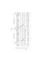
図4において、P1(1)〜P1(m)は、第1行〜第m行にそれぞれ対応する走査信号P1を示している。P3(1)〜P3(m)は第1行〜第m行にそれぞれ対応する輝度制御信号P3を示している。第1行と第2行、第3行と第4行、第5行と第6行、第m−1行と第m行はそれぞれ同一の発光期間制御信号が入力されるため、P3(1)=P3(2)、P3(3)=P3(4)、P3(5)=P3(6)、・・・、P3(m−1)=P3(m)となっている。図の煩雑化を避けるために記載していないが、走査信号P2に関しては、図3に記載のタイミングと同様にして出力される。
図5は、図4に示す表示装置の動作を実施する行制御回路3の一例である。
図7において、P1(1)〜P1(m)は、第1行〜第m行にそれぞれ対応する走査信号P1を示している。P3(1)〜P3(m)は第1行〜第m行にそれぞれ対応する輝度制御信号P3を示している。第1行と第2行、第3行と第4行、第5行と第6行、第m−1行と第m行はそれぞれ同一の発光期間制御信号が入力されるため、P3(1)=P3(2)、P3(3)=P3(4)、P3(5)=P3(6)、・・・、P3(m−1)=P3(m)となっている。図の煩雑化を避けるために記載していないが、走査信号P2に関しては、図3に記載のタイミングと同様にして出力される。
本実施例における発光期間制御信号P3は、同一のP3が入力される2つの行(例えば、第1行と第2行)のいずれかのP1がHighレベルの期間(電流プログラミング期間)である場合、必ずHighレベル期間(非発光期間)であり、かつ、電流プログラミング期間後、次回の電流プログラミングが行われるまでにLowレベル期間(発光期間)を複数回、設けている。
図10に示す表示装置では、行制御回路3A、行制御回路3Bを有している。図8におけるa部を行制御回路3A、b部を行制御回路3Bのように分離して配置しても良い。
図11において、画像表示部には、RGB原色数のEL素子と、このEL素子に入力される電流を制御するためのTFTから構成される画素回路2とが画素1を構成してm行×n列の2次元状に配列されている。ここでmは偶数、nは自然数とする。表示領域の周辺には行制御回路3、および列制御回路4を備えている。行制御回路3Cの各出力端子からは走査信号P1(1)〜P1(m)、P2(1)〜P2(m)と発光期間制御信号P3(1)〜P3(m)が出力される。走査信号は走査線5を介して各行の画素回路2に入力される。発光期間制御信号は発光期間制御線6を介して各行の画素回路2に入力される。図1とは異なり、発光期間制御線6は全行独立に画素回路2に入力される。列制御回路4には映像信号が入力され、各出力端子から電流データIdataが出力される。電流データIdataはデータ線7を介して各列の画素回路に入力される。
図12において、P1(1)〜P1(m)は、第1行〜第m行にそれぞれ対応する走査信号P1を示している。P3(1)〜P3(m)は第1行〜第m行にそれぞれ対応する輝度制御信号P3を示している。図の煩雑化を避けるために記載していないが、走査信号P2に関しては、図3に記載のタイミングと同様にして出力される。
図13において、行制御回路3Cは、フリップフロップ10からなるシフトレジスタ11Cを有しており、シフトレジスタ11Cの各出力はNOTゲート12、ANDゲート13、ORゲート16からなるロジック回路14Bに入力され、バッファ15を通じてP1、P2、P3を出力する構成となっている。簡略化のため、第1行から第6行までの出力について図示している。
図15は、本実施例のデジタルスチルカメラシステムの一例のブロック図である。図中、50はデジタルスチルカメラシステム、51は撮影部、52は映像信号処理回路、53は表示パネル、54はメモリ、55はCPU、56は操作部を示す。
2 画素回路
3、3A、3B、3C 行制御回路
4 列制御回路
5 走査線
6 発光期間制御線
7 データ線
10 フリップフロップ
11、11A、11B、11C シフトレジスタ
12 NOTゲート
13 ANDゲート
14、14A、14B ロジック回路
15 バッファ
16 ORゲート
50 デジタルスチルカメラシステム
51 撮影部
52 映像信号処理回路
53 表示パネル
54 メモリ
55 CPU
56 操作部
Claims (5)
- 電流に応じて発光輝度が制御される表示素子と、
電流の値が設定され、設定された電流を前記表示素子に供給する画素回路と、
前記表示素子と前記画素回路の組が行方向および列方向にマトリクス状に複数配置された画像表示部と、
前記画像表示部の行毎に設けられた走査線と、
前記画像表示部の行毎に設けられた発光期間制御線と、
前記画像表示部の行数に応じて配置され、前記画素回路が前記表示素子に供給する電流を設定する期間を制御する走査信号を前記走査線に出力し、かつ前記画素回路が前記表示素子に電流を供給する期間を制御する発光期間制御信号を前記発光期間制御線に出力する行制御回路と、
前記画像表示部の列毎に設けられたデータ線と、
前記画像表示部の列数に応じて配置され、前記画素回路が前記表示素子に供給する電流に応じたデータ信号を前記データ線に出力する列制御回路と、
を有する表示装置であって、
1フレームが、
前記行制御回路が前記画像表示部の奇数行の前記走査線に順次前記走査信号を出力し、前記列制御回路が前記データ信号を前記データ線に出力して、前記画像表示部の奇数行の表示素子に供給する電流を当該表示素子の前記画素回路に順次設定する第1の期間と、前記行制御回路が前記画像表示部の偶数行の前記走査線に順次前記走査信号を出力し、前記列制御回路が前記データ信号を前記データ線に出力して、前記画像表示部の偶数行の表示素子に供給する電流を当該表示素子の前記画素回路に順次設定する第2の期間と、からなり、
前記行制御回路が、前記走査信号が出力されている行の前記走査信号が出力されている期間を除き、前記画像表示部の奇数行および偶数行の前記発光期間制御線に、発光期間制御信号を出力して、前記第1の期間および前記第2の期間に、前記表示素子に、当該表示素子の前記画素回路内に設定された電流を複数回に分けて一定期間供給し、
前記発光期間制御信号の発光期間を決めるパルス幅および間隔は一様であって、かつ、前記発光期間制御信号の1周期は前記走査信号が出力されている期間と等しいことを特徴とする表示装置。 - 隣接する2行の前記発光期間制御線に同時に前記発光期間制御信号が出力されることを特徴とする請求項1に記載の表示装置。
- 前記行制御回路がシフトレジスタを含み、該シフトレジスタの入力信号の継続期間に等しい長さの時間、前記発光期間制御信号を生成することを特徴とする請求項1または2に記載の表示装置。
- 前記発光期間制御信号の生成期間が外部信号により制御されることを特徴とする請求項1ないし3のいずれか1項に記載の表示装置。
- 前記画素回路が前記表示素子に供給する電流の設定が、再度前記表示素子に供給する電流を設定するまで保持されていることを特徴とする請求項1ないし4のいずれか1項に記載の表示装置。
Priority Applications (4)
| Application Number | Priority Date | Filing Date | Title |
|---|---|---|---|
| JP2006098011A JP5058505B2 (ja) | 2006-03-31 | 2006-03-31 | 表示装置 |
| CN2007800113794A CN101410884B (zh) | 2006-03-31 | 2007-03-30 | 显示设备 |
| PCT/JP2007/057708 WO2007116950A1 (en) | 2006-03-31 | 2007-03-30 | Display device |
| US11/917,068 US7911425B2 (en) | 2006-03-31 | 2007-03-30 | Display device |
Applications Claiming Priority (1)
| Application Number | Priority Date | Filing Date | Title |
|---|---|---|---|
| JP2006098011A JP5058505B2 (ja) | 2006-03-31 | 2006-03-31 | 表示装置 |
Publications (3)
| Publication Number | Publication Date |
|---|---|
| JP2007271973A JP2007271973A (ja) | 2007-10-18 |
| JP2007271973A5 JP2007271973A5 (ja) | 2009-05-07 |
| JP5058505B2 true JP5058505B2 (ja) | 2012-10-24 |
Family
ID=38370979
Family Applications (1)
| Application Number | Title | Priority Date | Filing Date |
|---|---|---|---|
| JP2006098011A Expired - Fee Related JP5058505B2 (ja) | 2006-03-31 | 2006-03-31 | 表示装置 |
Country Status (4)
| Country | Link |
|---|---|
| US (1) | US7911425B2 (ja) |
| JP (1) | JP5058505B2 (ja) |
| CN (1) | CN101410884B (ja) |
| WO (1) | WO2007116950A1 (ja) |
Families Citing this family (22)
| Publication number | Priority date | Publication date | Assignee | Title |
|---|---|---|---|---|
| JP5495510B2 (ja) * | 2007-06-19 | 2014-05-21 | キヤノン株式会社 | 表示装置及びそれを用いた電子機器 |
| JP2009014836A (ja) * | 2007-07-02 | 2009-01-22 | Canon Inc | アクティブマトリクス型表示装置及びその駆動方法 |
| CN101779229B (zh) * | 2007-08-21 | 2012-11-07 | 佳能株式会社 | 显示装置及其驱动方法 |
| JP2009080272A (ja) * | 2007-09-26 | 2009-04-16 | Canon Inc | アクティブマトリクス型表示装置 |
| JP2009109641A (ja) * | 2007-10-29 | 2009-05-21 | Canon Inc | 駆動回路、及びアクティブマトリクス型表示装置 |
| JP4816686B2 (ja) * | 2008-06-06 | 2011-11-16 | ソニー株式会社 | 走査駆動回路 |
| JP2010008987A (ja) * | 2008-06-30 | 2010-01-14 | Canon Inc | 駆動回路 |
| JP2010122355A (ja) * | 2008-11-18 | 2010-06-03 | Canon Inc | 表示装置及びカメラ |
| JP5434092B2 (ja) * | 2009-01-27 | 2014-03-05 | セイコーエプソン株式会社 | 発光装置及び電子機器 |
| JP5284198B2 (ja) * | 2009-06-30 | 2013-09-11 | キヤノン株式会社 | 表示装置およびその駆動方法 |
| JP2011013415A (ja) * | 2009-07-01 | 2011-01-20 | Canon Inc | アクティブマトリックス型表示装置 |
| JP2011028135A (ja) * | 2009-07-29 | 2011-02-10 | Canon Inc | 表示装置及びその駆動方法 |
| KR101703875B1 (ko) * | 2010-08-20 | 2017-02-07 | 엘지디스플레이 주식회사 | 액정표시장치 및 그 구동방법 |
| US20120081347A1 (en) * | 2010-09-30 | 2012-04-05 | Apple Inc. | Low power inversion scheme with minimized number of output transitions |
| KR20120044507A (ko) * | 2010-10-28 | 2012-05-08 | 삼성모바일디스플레이주식회사 | 유기전계발광 표시장치 및 그의 구동방법 |
| JP6124573B2 (ja) | 2011-12-20 | 2017-05-10 | キヤノン株式会社 | 表示装置 |
| CN103116429A (zh) * | 2013-01-31 | 2013-05-22 | 敦泰科技有限公司 | 面向in-cell技术的扫描方法、装置、控制器和电子设备 |
| JP6478518B2 (ja) | 2014-08-11 | 2019-03-06 | キヤノン株式会社 | 発光装置及び画像形成装置 |
| KR102568899B1 (ko) * | 2016-11-04 | 2023-08-21 | 삼성전자주식회사 | Led 디스플레이 장치 및 그 동작 방법 |
| US11749157B2 (en) | 2022-01-25 | 2023-09-05 | Wuhan China Star Optoelectronics Semiconductor Display Technology Co., Ltd. | Display panel and display device |
| CN114420029B (zh) * | 2022-01-25 | 2023-08-22 | 武汉华星光电半导体显示技术有限公司 | 显示面板及显示装置 |
| CN119604921A (zh) * | 2023-06-20 | 2025-03-11 | 京东方科技集团股份有限公司 | 显示装置 |
Family Cites Families (14)
| Publication number | Priority date | Publication date | Assignee | Title |
|---|---|---|---|---|
| US7227517B2 (en) * | 2001-08-23 | 2007-06-05 | Seiko Epson Corporation | Electronic device driving method, electronic device, semiconductor integrated circuit, and electronic apparatus |
| JP4357413B2 (ja) * | 2002-04-26 | 2009-11-04 | 東芝モバイルディスプレイ株式会社 | El表示装置 |
| JP4490650B2 (ja) * | 2002-04-26 | 2010-06-30 | 東芝モバイルディスプレイ株式会社 | El表示装置の駆動方法、およびel表示装置 |
| JP2004191752A (ja) * | 2002-12-12 | 2004-07-08 | Seiko Epson Corp | 電気光学装置、電気光学装置の駆動方法および電子機器 |
| JP3950845B2 (ja) | 2003-03-07 | 2007-08-01 | キヤノン株式会社 | 駆動回路及びその評価方法 |
| WO2004086348A1 (en) | 2003-03-25 | 2004-10-07 | Canon Kabushiki Kaisha | Driving method of display apparatus in which a handwriting can be overweitten on the displayed image |
| JP4838498B2 (ja) | 2003-05-21 | 2011-12-14 | キヤノン株式会社 | 表示装置 |
| JP4054794B2 (ja) | 2003-12-04 | 2008-03-05 | キヤノン株式会社 | 駆動装置及び表示装置及び記録装置 |
| US7608861B2 (en) | 2004-06-24 | 2009-10-27 | Canon Kabushiki Kaisha | Active matrix type display having two transistors of opposite conductivity acting as a single switch for the driving transistor of a display element |
| JP4438066B2 (ja) | 2004-11-26 | 2010-03-24 | キヤノン株式会社 | アクティブマトリクス型表示装置およびその電流プログラミング方法 |
| JP4438067B2 (ja) | 2004-11-26 | 2010-03-24 | キヤノン株式会社 | アクティブマトリクス型表示装置およびその電流プログラミング方法 |
| JP4438069B2 (ja) | 2004-12-03 | 2010-03-24 | キヤノン株式会社 | 電流プログラミング装置、アクティブマトリクス型表示装置およびこれらの電流プログラミング方法 |
| JP4552844B2 (ja) * | 2005-06-09 | 2010-09-29 | セイコーエプソン株式会社 | 発光装置、その駆動方法および電子機器 |
| US7872617B2 (en) | 2005-10-12 | 2011-01-18 | Canon Kabushiki Kaisha | Display apparatus and method for driving the same |
-
2006
- 2006-03-31 JP JP2006098011A patent/JP5058505B2/ja not_active Expired - Fee Related
-
2007
- 2007-03-30 WO PCT/JP2007/057708 patent/WO2007116950A1/en not_active Ceased
- 2007-03-30 US US11/917,068 patent/US7911425B2/en not_active Expired - Fee Related
- 2007-03-30 CN CN2007800113794A patent/CN101410884B/zh not_active Expired - Fee Related
Also Published As
| Publication number | Publication date |
|---|---|
| US20090231239A1 (en) | 2009-09-17 |
| US7911425B2 (en) | 2011-03-22 |
| JP2007271973A (ja) | 2007-10-18 |
| WO2007116950A1 (en) | 2007-10-18 |
| CN101410884B (zh) | 2011-12-14 |
| CN101410884A (zh) | 2009-04-15 |
Similar Documents
| Publication | Publication Date | Title |
|---|---|---|
| JP5495510B2 (ja) | 表示装置及びそれを用いた電子機器 | |
| JP5058505B2 (ja) | 表示装置 | |
| JP4284558B2 (ja) | 表示駆動装置及び表示装置並びにその駆動制御方法 | |
| JP4552844B2 (ja) | 発光装置、その駆動方法および電子機器 | |
| US8514209B2 (en) | Display apparatus and method for driving the same | |
| CN109036279A (zh) | 阵列基板、驱动方法、有机发光显示面板及显示装置 | |
| JP4304585B2 (ja) | 電流生成供給回路及びその制御方法並びに該電流生成供給回路を備えた表示装置 | |
| CN101779229A (zh) | 显示装置及其驱动方法 | |
| TWI249151B (en) | Display device and driving method with this display device | |
| CN110400541B (zh) | 一种显示面板及显示装置 | |
| JP4314638B2 (ja) | 表示装置及びその駆動制御方法 | |
| CN113692612A (zh) | 显示装置、显示装置的驱动方法以及电子设备 | |
| CN112785969A (zh) | 具有发光驱动电路的电致发光显示面板 | |
| CN112735332B (zh) | 显示设备 | |
| JP2007133351A (ja) | 表示装置、アクティブマトリクス装置およびそれらの駆動方法 | |
| JP4337327B2 (ja) | ディスプレイ及び電子機器 | |
| KR100707626B1 (ko) | 발광표시장치 및 그의 구동방법 | |
| KR100581808B1 (ko) | 디멀티플렉서를 이용한 발광 표시장치 | |
| JP5207685B2 (ja) | 表示装置及びその駆動方法 | |
| JP3915906B2 (ja) | 電流駆動装置及びその駆動制御方法並びに電流駆動装置を用いた表示装置 | |
| KR100882674B1 (ko) | 유기전계발광표시장치 및 그의 구동방법 | |
| JP4941426B2 (ja) | 表示装置 | |
| JP2005043460A (ja) | 電子装置、電子装置の駆動方法、電気光学装置、電気光学装置の駆動方法及び電子機器 | |
| JP4617284B2 (ja) | 表示装置 | |
| JP2010156839A (ja) | 表示装置及び駆動方法 |
Legal Events
| Date | Code | Title | Description |
|---|---|---|---|
| A521 | Request for written amendment filed |
Free format text: JAPANESE INTERMEDIATE CODE: A523 Effective date: 20090324 |
|
| A621 | Written request for application examination |
Free format text: JAPANESE INTERMEDIATE CODE: A621 Effective date: 20090324 |
|
| RD04 | Notification of resignation of power of attorney |
Free format text: JAPANESE INTERMEDIATE CODE: A7424 Effective date: 20100201 |
|
| RD01 | Notification of change of attorney |
Free format text: JAPANESE INTERMEDIATE CODE: A7421 Effective date: 20100630 |
|
| A131 | Notification of reasons for refusal |
Free format text: JAPANESE INTERMEDIATE CODE: A131 Effective date: 20111108 |
|
| A521 | Request for written amendment filed |
Free format text: JAPANESE INTERMEDIATE CODE: A523 Effective date: 20120105 |
|
| A131 | Notification of reasons for refusal |
Free format text: JAPANESE INTERMEDIATE CODE: A131 Effective date: 20120508 |
|
| A521 | Request for written amendment filed |
Free format text: JAPANESE INTERMEDIATE CODE: A523 Effective date: 20120705 |
|
| TRDD | Decision of grant or rejection written | ||
| A01 | Written decision to grant a patent or to grant a registration (utility model) |
Free format text: JAPANESE INTERMEDIATE CODE: A01 Effective date: 20120731 |
|
| A01 | Written decision to grant a patent or to grant a registration (utility model) |
Free format text: JAPANESE INTERMEDIATE CODE: A01 |
|
| A61 | First payment of annual fees (during grant procedure) |
Free format text: JAPANESE INTERMEDIATE CODE: A61 Effective date: 20120801 |
|
| FPAY | Renewal fee payment (event date is renewal date of database) |
Free format text: PAYMENT UNTIL: 20150810 Year of fee payment: 3 |
|
| FPAY | Renewal fee payment (event date is renewal date of database) |
Free format text: PAYMENT UNTIL: 20150810 Year of fee payment: 3 |
|
| LAPS | Cancellation because of no payment of annual fees |