JP5048236B2 - Semiconductor light emitting device and method for manufacturing semiconductor light emitting device - Google Patents
Semiconductor light emitting device and method for manufacturing semiconductor light emitting device Download PDFInfo
- Publication number
- JP5048236B2 JP5048236B2 JP2005326270A JP2005326270A JP5048236B2 JP 5048236 B2 JP5048236 B2 JP 5048236B2 JP 2005326270 A JP2005326270 A JP 2005326270A JP 2005326270 A JP2005326270 A JP 2005326270A JP 5048236 B2 JP5048236 B2 JP 5048236B2
- Authority
- JP
- Japan
- Prior art keywords
- layer
- gallium nitride
- region
- conductivity type
- less
- Prior art date
- Legal status (The legal status is an assumption and is not a legal conclusion. Google has not performed a legal analysis and makes no representation as to the accuracy of the status listed.)
- Expired - Fee Related
Links
Images


Classifications
-
- H—ELECTRICITY
- H01—ELECTRIC ELEMENTS
- H01L—SEMICONDUCTOR DEVICES NOT COVERED BY CLASS H10
- H01L33/00—Semiconductor devices with at least one potential-jump barrier or surface barrier specially adapted for light emission; Processes or apparatus specially adapted for the manufacture or treatment thereof or of parts thereof; Details thereof
- H01L33/02—Semiconductor devices with at least one potential-jump barrier or surface barrier specially adapted for light emission; Processes or apparatus specially adapted for the manufacture or treatment thereof or of parts thereof; Details thereof characterised by the semiconductor bodies
- H01L33/26—Materials of the light emitting region
- H01L33/30—Materials of the light emitting region containing only elements of group III and group V of the periodic system
- H01L33/32—Materials of the light emitting region containing only elements of group III and group V of the periodic system containing nitrogen
-
- B—PERFORMING OPERATIONS; TRANSPORTING
- B82—NANOTECHNOLOGY
- B82Y—SPECIFIC USES OR APPLICATIONS OF NANOSTRUCTURES; MEASUREMENT OR ANALYSIS OF NANOSTRUCTURES; MANUFACTURE OR TREATMENT OF NANOSTRUCTURES
- B82Y20/00—Nanooptics, e.g. quantum optics or photonic crystals
-
- H—ELECTRICITY
- H01—ELECTRIC ELEMENTS
- H01L—SEMICONDUCTOR DEVICES NOT COVERED BY CLASS H10
- H01L33/00—Semiconductor devices with at least one potential-jump barrier or surface barrier specially adapted for light emission; Processes or apparatus specially adapted for the manufacture or treatment thereof or of parts thereof; Details thereof
- H01L33/02—Semiconductor devices with at least one potential-jump barrier or surface barrier specially adapted for light emission; Processes or apparatus specially adapted for the manufacture or treatment thereof or of parts thereof; Details thereof characterised by the semiconductor bodies
- H01L33/04—Semiconductor devices with at least one potential-jump barrier or surface barrier specially adapted for light emission; Processes or apparatus specially adapted for the manufacture or treatment thereof or of parts thereof; Details thereof characterised by the semiconductor bodies with a quantum effect structure or superlattice, e.g. tunnel junction
- H01L33/06—Semiconductor devices with at least one potential-jump barrier or surface barrier specially adapted for light emission; Processes or apparatus specially adapted for the manufacture or treatment thereof or of parts thereof; Details thereof characterised by the semiconductor bodies with a quantum effect structure or superlattice, e.g. tunnel junction within the light emitting region, e.g. quantum confinement structure or tunnel barrier
Description
本発明は、半導体発光素子、および半導体発光素子を作製する方法に関する。 The present invention relates to a semiconductor light emitting device and a method for manufacturing the semiconductor light emitting device.
特許文献1には、サファイア基板を用いる窒化ガリウム系化合物半導体発光素子が記載されている。特許文献1に記載された発明の目的は、厚さが等しい井戸層および障壁層からなる多層膜全体を一つの発光層とすることにより格子不整を緩和して、発光層の結晶性を向上する窒化物半導体発光素子を提供することにある。実施例1には、摂氏800度において障壁層および井戸層を成長する。井戸層は厚さ2nmのIn0.2Ga0.8Nからなり、障壁層は2nmのIn0.04Ga0.96Nからなる。実施例2には、摂氏800度において障壁層および井戸層を成長する。井戸層は厚さ5nmのIn0.2Ga0.8Nからなり、障壁層は5nmのIn0.04Ga0.96Nからなる。
特許文献2には、サファイア基板を用いる窒化物半導体発光素子が記載されている。特許文献2に記載された発明の目的は、緑色LEDのみならず360nm以上の発光波長で高輝度および高出力の窒化物半導体発光素子を提供することにある。実施例10の窒化物半導体発光素子は、1nm厚のノンドープIn0.15Ga0.85N井戸層と、1nm厚のノンドープIn0.05Ga0.95N障壁層とを含む量子井戸構造を有する。実施例11の窒化物半導体発光素子は、2.5nm厚のノンドープIn0.15Ga0.85N井戸層と、5nm厚のノンドープIn0.05Ga0.95N障壁層とを含む量子井戸構造を有する。これらの窒化物半導体発光素子は、415nmの発光波長を有している。活性層のインジウム組成を大きくすると結晶性が悪くなり、バンド間発光による520nm付近の緑色発光を得ることが難しい。しかしながら、上記の窒化物半導体発光素子では、熱膨張係数の小さいクラッド層で熱膨張係数の大きい活性層を挟むことにより活性層に引っ張り応力が加わるので、活性層のバンドギャップエネルギが本来の値よりも小さい。このため、この発光素子の井戸層を厚くすることはできない。
特許文献3には、サファイア基板を用いる窒化物半導体素子が記載されている。特許文献3に記載された発明の目的は、発光出力を低下させることなく、光電変換効率を向上できる窒化物半導体発光素子を提供することにある。実施例には、摂氏800度において障壁層および井戸層を成長する。井戸層は厚さ3nmのIn0.3Ga0.7Nからなり、障壁層は30nmのSiドープGaNからなる。
非特許文献1には、青色LED構造が記載されている。この青色LED構造のために、低温GaNバッファ層、ノンドープGaN層、n型GaN層、MQW活性層、p型AlGaN層、p型GaN層が、パターンが形成されたc面サファイア基板上に順にMOCVD法を用いて形成される。MQW構造は、3nm厚のノンドープIn0.3Ga0.7N井戸層と25nmのノンドープGaN障壁層によって構成されている。p電極は、メッシュ状のRh/Ir/Ptからなる。青色LED構造はエポキシ樹脂により封止されている。開口比率70%のメッシュ電極から電流20mA(メッシュ電極直下の電流密度105A/cm2、活性層において電流密度39A/cm2)を加えたとき、出力18.8mWが得られ、外部量子効率34.9%が得られる。しかしながら、メッシュ電極から電流100mA(活性層における電流密度で195A/cm2)を加えてとき、出力65mWが得られ、外部量子効率25%にまで低下する。
Non-Patent
非特許文献2には、量子井戸構造の発光ダイオードが記載されている。この発光ダイオードは、サファイア基板のc面上に低温で形成された核生成層、Siドープ下地層、InGaN/GaNからなるMQW発光層、p型AlGaN層およびp型GaN層を含む。428nm、454nm、501nm、545nmの発光波長を示すチップ(面積0.0007cm2)をフリップチップ実装し、デューティ1%および1kHzのパルス電流を印加した。最も効率の良い発光波長428nmにおいて、電流密度12.5A/cm2(0.0875A)で電力効率約28%が得られた。しかしながら、電流密度125A/cm2において約18%まで低下した。
Non-Patent
非特許文献3には、InGaN/GaN系発光ダイオードが記載されている。この文献によれば、InGaN系発光ダイオードにおいて、井戸層の厚みが増加すると、LEDの出力が低下する。
上記の文献に記載された発光素子に加えられる電流の密度が低いとき、発光素子の外部量子効率が高い。しかしながら、電流密度が高くなるにつれて、外部量子効率が低下する。InGaN系活性層を用いた青色発光素子(波長420nm以上490nm以下)では、低い電流密度では高い発光効率が得られている。この理由としては、インジウム組成のゆらぎに起因する局在準位が発光に寄与するので高い発光効率が得られていると考えられている。つまり、InGaN系活性層のインジウム組成の空間的な変化(ゆらぎ)に応じてポテンシャルも空間的に変化する。しかしながら、電流密度が大きくなると上記の局在準位からキャリアが溢れるようになり、局在準位の周辺も発光に寄与するようになる。これ故に、大きな電流密度では、全体としての発光効率が低下する。 When the density of the current applied to the light emitting element described in the above document is low, the external quantum efficiency of the light emitting element is high. However, as the current density increases, the external quantum efficiency decreases. In a blue light emitting element (wavelength of 420 nm or more and 490 nm or less) using an InGaN-based active layer, high luminous efficiency is obtained at a low current density. The reason for this is thought to be that high emission efficiency is obtained because the localized levels resulting from fluctuations in the indium composition contribute to light emission. That is, the potential also changes spatially according to the spatial change (fluctuation) of the indium composition of the InGaN-based active layer. However, when the current density is increased, carriers overflow from the above-mentioned localized levels, and the periphery of the localized levels also contributes to light emission. Therefore, at a large current density, the overall light emission efficiency decreases.
この発光効率の低下を小さくすることについて検討した結果によれば、高電流密度において発光効率の低下を小さくするためには、InGaN層のインジウム組成のゆらぎが小さいことが好ましい。インジウム組成を小さくすると、インジウム組成のゆらぎが小さくなる。ところが、単にインジウム組成を小さくしてインジウム組成のゆらぎを小さくするだけでは、発光波長が所望の波長からシフトしてしまう。 According to the result of examining the reduction in the luminous efficiency, it is preferable that the fluctuation of the indium composition of the InGaN layer is small in order to reduce the reduction in the luminous efficiency at a high current density. When the indium composition is reduced, the fluctuation of the indium composition is reduced. However, simply reducing the indium composition to reduce the fluctuation of the indium composition shifts the emission wavelength from the desired wavelength.
所望の波長で発光素子を発光させるためには、インジウム組成を小さくすることに加えて、InGaN井戸層の厚さを大きくすることが必要である。しかしながら、非特許文献3等に記載されているように、(0001)サファイア基板を用いるInGaN系発光ダイオードにおいて井戸層の厚みが増加すると、LEDの出力が低下することが知られている。
In order to cause the light emitting element to emit light at a desired wavelength, in addition to reducing the indium composition, it is necessary to increase the thickness of the InGaN well layer. However, as described in Non-Patent
本発明は、このような事情を鑑みてなされたものであり、高い電流に密度においても外部量子効率の低下が小さい半導体発光素子を提供することを目的としており、またこの半導体発光素子を作製する方法を提供することを目的とする。 The present invention has been made in view of such circumstances, and an object of the present invention is to provide a semiconductor light-emitting device in which a decrease in external quantum efficiency is small even at high current and density, and this semiconductor light-emitting device is manufactured. It aims to provide a method.
本発明の一側面によれば、半導体発光素子は、(a)1×107cm−2以下の貫通転位密度を有する第1導電型窒化ガリウム系クラッド層と、(b)第2導電型窒化ガリウム系クラッド層と、(c)複数の井戸層および障壁層を含む量子井戸構造を有しており前記第1導電型窒化ガリウム系クラッド層と前記第2導電型窒化ガリウム系クラッド層との間に設けられた活性領域とを備え、前記量子井戸構造は、420nm以上490nm以下の波長範囲内のピーク波長を有する光を発生するように設けられており、前記井戸層の各々は、アンドープInXGa1−XN(0<X<0.14、Xは歪み組成)領域を含み、前記井戸層の厚さが4nm以上であり、前記井戸層の厚さが10nm以下であり、前記障壁層は、アンドープInYGa1−YN(0≦Y≦0.05、Yは歪み組成、Y<X)領域を含む。 According to one aspect of the present invention, a semiconductor light emitting device includes: (a) a first conductivity type gallium nitride-based cladding layer having a threading dislocation density of 1 × 10 7 cm −2 or less; and (b) a second conductivity type nitridation. A gallium-based cladding layer; and (c) a quantum well structure including a plurality of well layers and barrier layers, and between the first-conductivity-type gallium nitride-based cladding layer and the second-conductivity-type gallium nitride-based cladding layer. The quantum well structure is provided to generate light having a peak wavelength in a wavelength range of 420 nm or more and 490 nm or less, and each of the well layers includes undoped In X Including a Ga 1-X N (0 <X <0.14, X is strain composition) region, the thickness of the well layer is 4 nm or more, the thickness of the well layer is 10 nm or less, and the barrier layer It is undoped an in Y a 1-Y N (0 ≦ Y ≦ 0.05, Y : strained composition, Y <X) containing area.
この半導体発光素子によれば、井戸層のIn組成Xが小さいので、In組成のゆらぎに起因した局在準位が井戸層において減少する。局在準位の減少により、活性領域は貫通転位密度に敏感になる。また、単に井戸層のIn組成Xを下げると発光波長がシフトするので、このシフトを無しに波長420nm以上490nm以下の波長範囲の光を得るために井戸層を厚くする。しかしながら、井戸層を厚くするとInGaN井戸層の結晶品質が低下する。転位に敏感になることおよび井戸層を厚くすることの影響を小さくするために、貫通転位密度1×107cm−2以下の下地層上に活性領域を設ける。このため、高電流密度での外部量子効率の低下を抑制できる。 According to this semiconductor light emitting device, since the In composition X of the well layer is small, the localized level due to the fluctuation of the In composition is reduced in the well layer. Due to the reduction of the localized levels, the active region becomes sensitive to threading dislocation density. Moreover, since the emission wavelength is shifted simply by reducing the In composition X of the well layer, the well layer is thickened to obtain light in the wavelength range of 420 nm to 490 nm without this shift. However, when the well layer is thickened, the crystal quality of the InGaN well layer is degraded. In order to reduce the effects of being sensitive to dislocations and increasing the thickness of the well layer, an active region is provided on the base layer having a threading dislocation density of 1 × 10 7 cm −2 or less. For this reason, it is possible to suppress a decrease in external quantum efficiency at a high current density.
本発明の別の側面によれば、半導体発光素子は、(a)1×107cm−2以下の貫通転位密度を有する第1導電型窒化ガリウム系クラッド層と、(b)第2導電型窒化ガリウム系クラッド層と、(c)複数の井戸層および障壁層を含む量子井戸構造を有しており前記第1導電型窒化ガリウム系クラッド層と前記第2導電型窒化ガリウム系クラッド層との間に設けられた活性領域とを備え、前記量子井戸構造は、波長420nm以上490nm以下の波長範囲内のピーク波長を有する光を発生するように設けられており、前記井戸層の各々は、アンドープInXGa1−XN(0<X<0.14、Xは歪み組成)領域を含み、前記井戸層の厚さが4nm以上であり、前記井戸層の厚さが10nm以下であり、前記障壁層は、n型ドーパントを含むInYGa1−YN(0≦Y≦0.05、Yは歪み組成、Y<X)領域を含む。
According to another aspect of the present invention, a semiconductor light emitting device includes (a) a first conductivity type gallium nitride cladding layer having a threading dislocation density of 1 × 10 7 cm −2 or less, and (b) a second conductivity type. A gallium nitride cladding layer; and (c) a quantum well structure including a plurality of well layers and barrier layers, and the first conductivity type gallium nitride cladding layer and the second conductivity type gallium nitride cladding layer. The quantum well structure is provided so as to generate light having a peak wavelength within a wavelength range of 420 nm or more and 490 nm or less, and each of the well layers is undoped. In X Ga 1-X N (0 <X <0.14, X is strain composition) region, the thickness of the well layer is 4 nm or more, the thickness of the well layer is 10 nm or less, Barrier layer is n-
この半導体発光素子によれば、井戸層のIn組成Xが小さいので、In組成のゆらぎに起因した局在準位が井戸層において減少する。局在準位の減少により、活性領域は貫通転位密度に敏感になる。また、単に井戸層のIn組成Xを下げると発光波長がシフトするので、このシフトを無しに波長420nm以上490nm以下の波長範囲の光を得るために井戸層を厚くする。しかしながら、井戸層を厚くするとInGaN井戸層の結晶品質が低下する。また、InGaN井戸層の厚みを厚くすると、順方向電圧Vfが上昇する。転位に敏感になることおよび井戸層を厚くすることの影響を小さくするために、貫通転位密度1×107cm−2以下の下地層上に活性領域を設ける。加えて、順方向電圧Vfの上昇は、障壁層にSiをドープすることにより小さくできる。このため、高電流密度での外部量子効率の低下を抑制できる。 According to this semiconductor light emitting device, since the In composition X of the well layer is small, the localized level due to the fluctuation of the In composition is reduced in the well layer. Due to the reduction of the localized levels, the active region becomes sensitive to threading dislocation density. Moreover, since the emission wavelength is shifted simply by reducing the In composition X of the well layer, the well layer is thickened to obtain light in the wavelength range of 420 nm to 490 nm without this shift. However, when the well layer is thickened, the crystal quality of the InGaN well layer is degraded. Further, when the thickness of the InGaN well layer is increased, the forward voltage Vf increases. In order to reduce the effects of being sensitive to dislocations and increasing the thickness of the well layer, an active region is provided on the base layer having a threading dislocation density of 1 × 10 7 cm −2 or less. In addition, the increase in the forward voltage Vf can be reduced by doping the barrier layer with Si. For this reason, it is possible to suppress a decrease in external quantum efficiency at a high current density.
本発明に係る半導体発光素子では、前記井戸層の厚さが4nm以上であることが好ましい。また、井戸層の厚さが10nm以下であることが好ましい。 In the semiconductor light emitting device according to the present invention, the thickness of the well layer is preferably 4 nm or more. Moreover, it is preferable that the thickness of a well layer is 10 nm or less.
この半導体発光素子によれば、InGaN井戸層の厚みを厚くすると、高電流密度での外部量子効率の低下が起こりにくくなると考えられる。 According to this semiconductor light emitting device, it is considered that when the thickness of the InGaN well layer is increased, the external quantum efficiency is hardly lowered at a high current density.
本発明に係る半導体発光素子は、(d)主面を有するIII族窒化物基板を更に備え、前記第1導電型窒化ガリウム系クラッド層、前記活性領域および前記第2導電型窒化ガリウム系クラッド層を含む半導体領域は、前記III族窒化物基板の前記主面上に設けられている。 The semiconductor light emitting device according to the present invention further comprises (d) a group III nitride substrate having a main surface, and the first conductivity type gallium nitride cladding layer, the active region, and the second conductivity type gallium nitride cladding layer. The semiconductor region containing is provided on the main surface of the group III nitride substrate.
この半導体発光素子によれば、基板がIII族窒化物半導体からなるので、基板と井戸層のInGaNとの格子定数差を小さくすることができ、InGaN井戸層の結晶品質の低下を抑えることができる。 According to this semiconductor light emitting device, since the substrate is made of a group III nitride semiconductor, the difference in lattice constant between the substrate and the InGaN of the well layer can be reduced, and the deterioration of the crystal quality of the InGaN well layer can be suppressed. .
本発明に係る半導体発光素子では、前記III族窒化物基板は貫通転位密度1×107cm−2以下であることが好ましい。この半導体発光素子では、基板の貫通転位密度が1×107cm−2以下であると下地層や井戸層のInGaN結晶に引き継がれる貫通転位の数も少なくなり、InGaN井戸層の厚みを大きくしたときも、InGaN井戸層の結晶品質の低下を縮小できる。 In the semiconductor light emitting device according to the present invention, the group III nitride substrate preferably has a threading dislocation density of 1 × 10 7 cm −2 or less. In this semiconductor light emitting device, when the threading dislocation density of the substrate is 1 × 10 7 cm −2 or less, the number of threading dislocations inherited by the InGaN crystal of the underlayer or well layer is reduced, and the thickness of the InGaN well layer is increased. Sometimes, the deterioration of the crystal quality of the InGaN well layer can be reduced.
本発明に係る半導体発光素子では、前記III族窒化物基板は貫通転位密度1×107cm−2以下である窒化ガリウム基板であることが好ましい。この半導体発光素子では、窒化ガリウム基板の貫通転位密度が1×107cm−2以下であると下地層や井戸層のInGaN結晶に引き継がれる貫通転位の数も少なくなり、InGaN井戸層の厚みを大きくしたときも、InGaN井戸層の結晶品質の低下を縮小できる。 In the semiconductor light emitting device according to the present invention, the group III nitride substrate is preferably a gallium nitride substrate having a threading dislocation density of 1 × 10 7 cm −2 or less. In this semiconductor light emitting device, when the threading dislocation density of the gallium nitride substrate is 1 × 10 7 cm −2 or less, the number of threading dislocations inherited by the InGaN crystal of the underlayer or well layer is reduced, and the thickness of the InGaN well layer is reduced. Even when it is increased, the decrease in crystal quality of the InGaN well layer can be reduced.
本発明の更なる別の側面は、半導体発光素子を作製する方法である。この方法は、(a)420nm以上490nm以下の波長範囲内のピーク波長を有する光を発生するように設けられた量子井戸構造を有する活性領域を貫通転位密度1×107cm−2以下の第1導電型の窒化ガリウム系クラッド領域上に形成する工程と、(b)前記活性領域上に第2導電型の別の窒化ガリウム系クラッド領域を形成する工程と、を備え、前記井戸層の成膜温度は前記障壁層の成膜温度より小さく、前記量子井戸構造の井戸層はアンドープInXGa1−XN(0<X<0.14、Xは歪み組成)領域を含み、前記井戸層の厚さが4nm以上であり、前記井戸層の厚さが10nm以下であり、前記量子井戸構造の障壁層はアンドープInYGa1−YN(0≦Y≦0.05、Yは歪み組成)領域を含む。 Yet another aspect of the present invention is a method of fabricating a semiconductor light emitting device. In this method, (a) an active region having a quantum well structure provided so as to generate light having a peak wavelength within a wavelength range of 420 nm or more and 490 nm or less is passed through an active region having a threading dislocation density of 1 × 10 7 cm −2 or less . forming on one conductivity type gallium nitride based cladding region, (b) and a step of forming another gallium nitride-based cladding region of the second conductivity type on the active region, formed of the well layer The film temperature is lower than the film formation temperature of the barrier layer, and the well layer of the quantum well structure includes an undoped In X Ga 1-X N (0 <X <0.14, X is a strain composition) region, and the well layer The well layer has a thickness of 10 nm or less, and the barrier layer of the quantum well structure is undoped In Y Ga 1-Y N (0 ≦ Y ≦ 0.05, Y is a strain composition) ) Including the area.
この方法によれば、井戸層の成膜温度を障壁層の成膜温度より小さくすると共に、井戸層のIn組成を低くすることによって、In組成ゆらぎが抑制される。このため、高電流密度での外部量子効率の低下を抑制できる。井戸層のIn組成を低くすると、In組成ゆらぎに起因した局在準位の数が減少する。ところが、局在準位の減少により、活性領域は、転位の影響を強く受けるようになる。つまり、活性領域の結晶品質は、活性領域および下地層の貫通転位密度に敏感になる。また、単に井戸層のIn組成を下げると、発光波長がシフトしてしまう。このシフトを防ぎ波長420nm以上490nm以下の発光を得るために、井戸層の厚みを増加する必要がある。井戸層を厚くするとInGaN井戸層の結晶品質が低下する。転位に敏感になることおよび井戸層を厚くすることの影響を小さくするために、下地層の貫通転位密度1×107cm−2以下とする。 According to this method, the In composition fluctuation is suppressed by making the well layer deposition temperature lower than the barrier layer deposition temperature and lowering the In composition of the well layer. For this reason, it is possible to suppress a decrease in external quantum efficiency at a high current density. When the In composition of the well layer is lowered, the number of localized levels due to fluctuations in the In composition is reduced. However, the active region is strongly influenced by the dislocation due to the decrease of the localized level. That is, the crystal quality of the active region is sensitive to the threading dislocation density of the active region and the underlying layer. Further, simply reducing the In composition of the well layer shifts the emission wavelength. In order to prevent this shift and obtain light emission with a wavelength of 420 nm or more and 490 nm or less, it is necessary to increase the thickness of the well layer. When the well layer is thickened, the crystal quality of the InGaN well layer is degraded. In order to reduce the influence of becoming sensitive to dislocations and increasing the thickness of the well layer, the threading dislocation density of the base layer is set to 1 × 10 7 cm −2 or less.
本発明の更なる別の側面は、半導体発光素子を作製する方法である。この方法は、(a)420nm以上490nm以下の波長範囲内のピーク波長を有する光を発生するように設けられた量子井戸構造を有する活性領域を貫通転位密度1×107cm−2以下の第1導電型の窒化ガリウム系クラッド領域上に形成する工程と、(b)前記活性領域上に第2導電型の別の窒化ガリウム系クラッド領域を形成する工程と、を備え、前記井戸層の成膜温度は前記障壁層の成膜温度より小さく、前記量子井戸構造の井戸層はアンドープInXGa1−XN(0<X<0.14、Xは歪み組成)領域を含み、前記井戸層の厚さが4nm以上であり、前記井戸層の厚さが10nm以下であり、前記量子井戸構造の障壁層はn型ドーパントを含むInYGa1−YN(0≦Y≦0.05、Yは歪み組成、Y<X)領域を含む。
Yet another aspect of the present invention is a method of fabricating a semiconductor light emitting device. In this method, (a) an active region having a quantum well structure provided so as to generate light having a peak wavelength within a wavelength range of 420 nm or more and 490 nm or less is passed through an active region having a threading dislocation density of 1 × 10 7 cm −2 or less . forming on one conductivity type gallium nitride based cladding region, (b) and a step of forming another gallium nitride-based cladding region of the second conductivity type on the active region, formed of the well layer The film temperature is lower than the film formation temperature of the barrier layer, and the well layer of the quantum well structure includes an undoped In X Ga 1-X N (0 <X <0.14, X is a strain composition) region, and the well layer The well layer has a thickness of 10 nm or less, and the barrier layer of the quantum well structure includes In Y Ga 1-Y N (0 ≦ Y ≦ 0.05, n-type dopant). Y is strain composition, Y <X) region Including.
この方法によれば、井戸層の成膜温度を障壁層の成膜温度より小さくすると共に、井戸層のIn組成を低くすることによって、In組成ゆらぎが抑制される。このため、高電流密度での外部量子効率の低下を抑制できる。井戸層のIn組成を低くすると、In組成ゆらぎに起因した局在準位が減少する。ところが、局在準位の減少により、活性領域は、転位の影響を強く受けるようになる。つまり、活性領域の結晶品質は、活性領域および下地層の貫通転位密度に敏感になる。また、単に井戸層のIn組成を下げると、発光波長がシフトしてしまう。このシフトを防ぎ波長420nm以上490nm以下の発光を得るために、井戸層の厚みを増加させる。井戸層を厚くするとInGaN井戸層の結晶品質が低下する。下地層の貫通転位密度が1×107cm−2以下であれば、転位に敏感になることおよび井戸層を厚くすることの影響を小さくできる。また、InGaN井戸層の厚みを厚くすると、順方向電圧Vfが上昇するけれども、障壁層にSiをドープすることにより順方向電圧Vfの増加を小さくすることができる。 According to this method, the In composition fluctuation is suppressed by making the well layer deposition temperature lower than the barrier layer deposition temperature and lowering the In composition of the well layer. For this reason, it is possible to suppress a decrease in external quantum efficiency at a high current density. When the In composition of the well layer is lowered, the localized level caused by the In composition fluctuation is reduced. However, the active region is strongly influenced by the dislocation due to the decrease of the localized level. That is, the crystal quality of the active region is sensitive to the threading dislocation density of the active region and the underlying layer. Further, simply reducing the In composition of the well layer shifts the emission wavelength. In order to prevent this shift and obtain light emission with a wavelength of 420 nm or more and 490 nm or less, the thickness of the well layer is increased. When the well layer is thickened, the crystal quality of the InGaN well layer is degraded. If the threading dislocation density of the underlayer is 1 × 10 7 cm −2 or less, the effects of becoming sensitive to dislocations and increasing the thickness of the well layer can be reduced. Further, when the thickness of the InGaN well layer is increased, the forward voltage Vf increases, but the increase of the forward voltage Vf can be reduced by doping Si into the barrier layer.
本発明に係る方法では、前記井戸層の厚さが4nm以上であることが好ましく、また井戸層の厚さが10nm以下であることが好ましい。この方法によれば、InGaN井戸層の厚みを厚くすると、高電流密度での外部量子効率の低下が起こりにくくなると考えられる。 In the method according to the present invention, the thickness of the well layer is preferably 4 nm or more, and the thickness of the well layer is preferably 10 nm or less. According to this method, it is considered that when the thickness of the InGaN well layer is increased, the external quantum efficiency is hardly lowered at a high current density.
本発明に係る方法は、(b)前記窒化ガリウム系クラッド領域をIII族窒化物基板上に成長する工程を更に備えることができる。この方法によれば、基板がIII族窒化物半導体からなるので、井戸層のInGaNと基板のIII族窒化物半導体との格子定数差を小さくすることができ、InGaN井戸層の結晶品質の低下を抑えることができる。 The method according to the present invention may further comprise (b) a step of growing the gallium nitride based cladding region on the group III nitride substrate. According to this method, since the substrate is made of a group III nitride semiconductor, the difference in lattice constant between the InGaN of the well layer and the group III nitride semiconductor of the substrate can be reduced, and the crystal quality of the InGaN well layer is reduced. Can be suppressed.
本発明に係る方法では、前記III族窒化物基板の貫通転位密度は1×107cm−2以下であることが好ましい。この方法では、基板の貫通転位密度が1×107cm−2以下であると下地層や井戸層のInGaN結晶に引き継がれる貫通転位の数も少なくなり、InGaN井戸層を厚くしても、InGaN井戸層の結晶品質への貫通転位の影響を小さくできる。 In the method according to the present invention, the threading dislocation density of the group III nitride substrate is preferably 1 × 10 7 cm −2 or less. In this method, when the threading dislocation density of the substrate is 1 × 10 7 cm −2 or less, the number of threading dislocations inherited by the InGaN crystal of the underlayer and the well layer is reduced, and even if the InGaN well layer is made thick, the InGaN The influence of threading dislocations on the crystal quality of the well layer can be reduced.
本発明に係る方法では、前記III族窒化物基板は貫通転位密度1×107cm−2以下である窒化ガリウム基板であることが好ましい。この方法では、窒化ガリウム基板の貫通転位密度が1×107cm−2以下であるので、井戸層のInGaN結晶における貫通転位の数も少なくなり、InGaN井戸層を厚くしたときも、InGaN井戸層の結晶品質の低下が縮小できる。 In the method according to the present invention, the group III nitride substrate is preferably a gallium nitride substrate having a threading dislocation density of 1 × 10 7 cm −2 or less. In this method, since the threading dislocation density of the gallium nitride substrate is 1 × 10 7 cm −2 or less, the number of threading dislocations in the InGaN crystal of the well layer is reduced, and even when the InGaN well layer is thickened, the InGaN well layer The decrease in crystal quality can be reduced.
本発明の上記の目的および他の目的、特徴、並びに利点は、添付図面を参照して進められる本発明の好適な実施の形態の以下の詳細な記述から、より容易に明らかになる。 The above and other objects, features, and advantages of the present invention will become more readily apparent from the following detailed description of preferred embodiments of the present invention, which proceeds with reference to the accompanying drawings.
以上説明したように、本発明によれば、高い電流に密度においても外部量子効率の低下が小さい半導体発光素子が提供されると共に、この半導体発光素子を作製する方法が提供される。 As described above, according to the present invention, there is provided a semiconductor light emitting device in which a decrease in external quantum efficiency is small even at a high current and density, and a method for manufacturing this semiconductor light emitting device is provided.
本発明の知見は、例示として示された添付図面を参照して以下の詳細な記述を考慮することによって容易に理解できる。引き続いて、添付図面を参照しながら、本発明の半導体発光素子、および半導体発光素子を作製する方法に係る実施の形態を説明する。可能な場合には、同一の部分には同一の符号を付する。 The knowledge of the present invention can be easily understood by considering the following detailed description with reference to the accompanying drawings shown as examples. Subsequently, embodiments of the semiconductor light emitting device of the present invention and the method for manufacturing the semiconductor light emitting device will be described with reference to the accompanying drawings. Where possible, the same parts are denoted by the same reference numerals.
(第1の実施の形態)
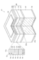
図1は、本実施の形態に係る半導体発光素子を示す図面である。この半導体発光素子は、例えば発光ダイオードであることができる。半導体発光素子11は、第1導電型の窒化ガリウム系クラッド層13と、第2導電型の窒化ガリウム系クラッド層15と、活性領域17とを含む。窒化ガリウム系クラッド層13は、1×107cm−2以下の貫通転位密度を有する。活性領域17は、第1導電型の窒化ガリウム系クラッド層13と第2導電型の窒化ガリウム系クラッド層15との間に設けられている。活性領域17は、複数の井戸層19および障壁層21を含む量子井戸構造17aを有しており、また量子井戸構造17aは420nm以上490nm以下の波長範囲内のピーク波長を有する光を発生するように設けられている。井戸層19の各々は、アンドープInXGa1−XN(0<X<0.14、Xは歪み組成)領域を含む。障壁層21は、アンドープInYGa1−YN(0≦Y≦0.05、Yは歪み組成、Y<X)領域を含む。ここで、本実施の形態では、インジウム組成Xは、歪み組成で示されており、緩和組成ではない。歪み組成とは結晶が下地結晶のa軸に格子整合して歪んでいることを仮定した組成であり、緩和組成とは結晶が下地結晶の影響を受けておらず歪んでいないことを仮定した組成である。
(First embodiment)
FIG. 1 is a drawing showing a semiconductor light emitting device according to the present embodiment. The semiconductor light emitting element can be, for example, a light emitting diode. The semiconductor
この半導体発光素子11によれば、井戸層19のIn組成(0<X<0.14、Xは歪み組成)が小さいので、In組成Xの空間的なゆらぎが抑制され、またこのゆらぎに起因した局在準位の数が少なくなる。しかしながら、局在準位の減少により、活性領域は、むしろ転位の影響を強く受けるようになる。つまり、厚い井戸層19の結晶品質は、これまで以上に活性領域17および下地層(例えば、領域13)の貫通転位密度に敏感になる。また、単に井戸層19のIn組成Xを下げると、発光波長がシフトしてしまう。このシフトを無しに波長420nm以上490nm以下の波長範囲の光を得るために、井戸層19の厚みDWを厚くする。ところが、井戸層19の厚みDWを厚くすると井戸層19の結晶品質が低下する。転位に敏感になることおよび井戸層19を厚くすることの影響を小さくするために、1×107cm−2以下の貫通転位密度を有する下地層上に活性領域17を設ける。これ故、半導体発光素子11の外部量子効率の低下を高電流密度において抑制できる。
According to the semiconductor
半導体発光素子11では、窒化ガリウム系クラッド層13および窒化ガリウム系クラッド層15のバンドギャップエネルギは井戸層19のバンドギャップエネルギより大きい。窒化ガリウム系クラッド層13は、例えばGaN、AlGaNからなる。窒化ガリウム系クラッド層15は、例えばAlGaN、GaNからなる。
In the semiconductor
多くの青色発光ダイオードでは、井戸層の厚みとして3nm程度を用いているけれども、インジウム組成を値を小さくしているので各井戸層19の厚さは4nm以上であることが好ましい。4nm以上にすると電流密度を上げたとき外部量子効率の低下を小さくできるという利点がある。また、各井戸層19の厚さが10nm以下であることが好ましい。10nm以下にするとInGaN井戸層の結晶品質が良好になるという利点がある。この半導体発光素子によれば、InGaN井戸層19の厚みを厚くすると、厚いInGaN井戸層のIn組成のゆらぎが小さくなる一方で、In組成のゆらぎによる局在準位の総和は、厚いInGaN井戸層の全体で増加する。In組成のゆらぎの縮小と共に井戸層の全体での局在準位の増加により、低電流密度での外部量子効率を維持できると共に高電流密度での外部量子効率の低下が起こりにくくなると考えられる。InGaN井戸層19の厚みDWを大きくするとInGaN井戸層19の結晶品質が低下する可能性があるけれども、下地層の貫通転位密度が1×107cm−2以下であるので、InGaN井戸層19の結晶品質の低下を抑えることができる。
In many blue light emitting diodes, the thickness of the well layer is about 3 nm. However, since the indium composition is reduced, the thickness of each
半導体発光素子11は、III族窒化物基板23を更に備えることができる。基板がIII族窒化物半導体をからなるので、井戸層19のInGaNと基板23との格子定数差を小さくすることができ、InGaN井戸層19の結晶品質の低下を抑えることができる。また、III族窒化物基板23は貫通転位密度1×107cm−2以下であることが好ましい。この半導体発光素子11では、基板23の貫通転位密度が1×107cm−2以下であると下地層や井戸層19のInGaN結晶に引き継がれる貫通転位の数も少なくなり、InGaN井戸層19の厚みDWを大きくしたときも、InGaN井戸層19の結晶品質の低下を縮小できる。III族窒化物基板23は窒化ガリウム基板であることが好ましい。窒化ガリウム基板は、貫通転位密度1×107cm−2以下である窒化ガリウムからなる。この窒化ガリウム上に下地層や井戸層を成長すれば、InGaN結晶に引き継がれる貫通転位の数も少なくなり、InGaN井戸層の結晶品質が良好になる。
The semiconductor
III族窒化物基板23の表面23a上には、半導体領域25が設けられている。半導体領域25は、窒化ガリウム系クラッド層13、活性領域17および窒化ガリウム系クラッド層15を含んでおり、さらに第1導電型の窒化ガリウム系半導体中間層27と、第2導電型のコンタクト層29とを含む。半導体発光素子11は、第2導電型のコンタクト層29に設けられた第1のオーミック電極31と、基板23の裏面23bに設けられた第2のオーミック電極33とを含む。
A
半導体発光素子11の一例として、発光ダイオードは
窒化ガリウム系クラッド層13:n−GaN(Siドープ)
窒化ガリウム系クラッド層15:p−Al0.12Ga0.88N(Mgドープ)
活性領域17の井戸層19:In0.11Ga0.89N(歪み組成)、5nm
活性領域17の障壁層21:In0.01Ga0.99N(歪み組成)、15nm
窒化ガリウム系半導体中間層27:n−Al0.12Ga0.88N
コンタクト層29:p−GaN
第1のオーミック電極31(アノード):Ni/Au(半透明電極)
第2のオーミック電極33(カソード):Ti/Al
を含む。
As an example of the semiconductor
Gallium nitride cladding layer 15: p-Al 0.12 Ga 0.88 N (Mg doped)
Well
Gallium nitride based semiconductor intermediate layer 27: n-Al 0.12 Ga 0.88 N
Contact layer 29: p-GaN
First ohmic electrode 31 (anode): Ni / Au (translucent electrode)
Second ohmic electrode 33 (cathode): Ti / Al
including.
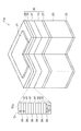
図2は、本実施の形態に係る半導体発光素子の変形例を示す図面である。半導体発光素子11aは、活性領域37を有している。活性領域37は、複数の井戸層39および障壁層41を含む量子井戸構造37aを有しており、また量子井戸構造37aは420nm以上490nm以下の波長範囲内のピーク波長を有する光を発生するように設けられている。井戸層39の各々は、アンドープInXGa1−XN(0<X<0.14、Xは歪み組成)領域を含む。障壁層41は、n型ドーパントを含むInYGa1−YN(0≦Y≦0.05、Yは歪み組成、Y<X)領域を含む。本実施の形態のインジウム組成X、Yは、歪み組成で示されており、緩和組成ではない。半導体領域35は、窒化ガリウム系クラッド層13、活性領域37および窒化ガリウム系クラッド層15を含んでおり、さらに第1導電型の窒化ガリウム系半導体中間層27と、第2導電型のコンタクト層29とを含む。
FIG. 2 is a view showing a modification of the semiconductor light emitting device according to the present embodiment. The semiconductor
この半導体発光素子11aでは、井戸層39のIn組成(0<X<0.14、Xは歪み組成)を小さくするので、In組成Xの空間的なゆらぎが抑制され、またこのゆらぎに起因した局在準位の数が少なくなる。ところが、局在準位の減少により、活性領域は、むしろ転位の影響を強く受けるようになる。つまり、活性領域37の結晶品質は、これまで以上に、活性領域37および下地層(例えば、領域13)の貫通転位密度に敏感になる。また、単に井戸層39のIn組成Xを下げると、発光波長がシフトしてしまう。このシフトを無しに420nm以上490nm以下の波長範囲の光を得るために、井戸層39の厚みDWを厚くする。しかしながら、井戸層39の厚みDWを厚くすると井戸層39の結晶品質が低下する。また、InGaN井戸層39の厚みを厚くすると、順方向電圧Vfが上昇する。転位に敏感になることおよび井戸層39を厚くすることの影響を小さくするために、1×107cm−2以下の貫通転位密度を有する下地層上に活性領域37を設けると共に、障壁層41にn型ドーパント(例えば、Si)をドープすることにより順方向電圧Vfの増加を小さくする。このため、半導体発光素子11aの外部量子効率の低下を高電流密度において抑制できる。
In this semiconductor
(実験例1):好適な例
有機金属気相成長法を用いて、青色(波長420nm以上490nm以下)発光ダイオードを作製する。原料には、トリメチルガリウム(TMGa)、トリメチルアルミニウム(TMAl)、トリメチルインジウム(TMIn)、アンモニア(NH3)、モノシラン(SiH4)、シクロペンタジエニルマグネシウム(Cp2Mg)を用いることができる。(0001)C面を有する窒化ガリウム基板を準備する。窒化ガリウム基板はn導電性を示し、また貫通転位密度は1×106cm−2である。有機金属気相成長炉のサセプタ上に窒化ガリウム基板を配置する。次いで、窒化ガリウム基板のサーマルクリーニングを行う。サーマルクリーニングの条件は、炉内圧力30kPaに制御しながらアンモニアガス(NH3)および水素ガス(H2)を有機金属気相成長炉に供給して、摂氏1050度の基板温度で10分間の熱処理を行う。
(Experimental example 1): Suitable example A blue (wavelength 420 nm or more and 490 nm or less) light emitting diode is produced using metal organic vapor phase epitaxy. As a raw material, trimethylgallium (TMGa), trimethylaluminum (TMAl), trimethylindium (TMIn), ammonia (NH 3 ), monosilane (SiH 4 ), cyclopentadienylmagnesium (Cp 2 Mg) can be used. A gallium nitride substrate having a (0001) C plane is prepared. The gallium nitride substrate exhibits n conductivity, and the threading dislocation density is 1 × 10 6 cm −2 . A gallium nitride substrate is placed on the susceptor of the metal organic chemical vapor deposition reactor. Next, thermal cleaning of the gallium nitride substrate is performed. The thermal cleaning condition is that ammonia gas (NH 3 ) and hydrogen gas (H 2 ) are supplied to the metal organic vapor phase growth furnace while controlling the pressure in the furnace at 30 kPa, and heat treatment is performed at a substrate temperature of 1050 degrees Celsius for 10 minutes. I do.
続いて、成膜工程を行う。摂氏1050度の基板温度および炉内圧力101kPaに変更した後に、原料ガス(TMGa、TMAl、NH3、SiH4)を用いて、厚さ50nmのn型Al0.12Ga0.88N中間層を成長する。炉内圧力101kPaを維持すると共に摂氏1100度の基板温度に変更した後に、原料ガス(TMGa、NH3、SiH4)を用いて、厚さ2μmのn型GaNバッファ層を成長する。バッファ層の成長速度は、4μm/hである。次いで、障壁層および井戸層を交互に成長する。障壁層の成長では、101kPaの炉内圧力を維持すると共に摂氏900度の基板温度に変更した後に、原料ガス(TMGa、TMIn、NH3)を用いて、厚さ15nmのアンドープIn0.01Ga0.99N層を堆積する。井戸層の成長では、101kPaの炉内圧力を維持すると共に摂氏800度の基板温度に変更した後に、原料ガス(TMGa、TMIn、NH3)を用いて、厚さ5nmのアンドープIn0.11Ga0.89N層を堆積する。井戸層および障壁層の成長は、必要な回数だけ繰り返される。本実施例では、6周期の量子井戸構造を形成する。上記の井戸層および障壁層は歪み組成で示されており、歪み組成In0.01Ga0.99N障壁層およびIn0.11Ga0.89N井戸層は、それぞれ、緩和組成In0.02Ga0.98N障壁層およびIn0.17Ga0.89N井戸層である。多くの場合に緩和組成で表現される。その後、炉内圧力101kPaを維持すると共に摂氏1050度の基板温度に変更した後に、原料ガス(TMGa、TMAl、NH3、Cp2Mg)を用いて、厚さ20nmのp型Al0.12Ga0.88Nクラッド層を成長する。次いで、原料ガス(TMGa、NH3、Cp2Mg)を用いて、厚さ150nmのp型GaNコンタクト層を成長する。これによりLEDエピタキシャル基板が完成する。 Subsequently, a film forming process is performed. After changing to a substrate temperature of 1050 degrees Celsius and a furnace pressure of 101 kPa, an n-type Al 0.12 Ga 0.88 N intermediate layer having a thickness of 50 nm is formed using source gases (TMGa, TMAl, NH 3 , SiH 4 ). To grow. After maintaining the furnace pressure of 101 kPa and changing the substrate temperature to 1100 degrees Celsius, an n-type GaN buffer layer having a thickness of 2 μm is grown using a source gas (TMGa, NH 3 , SiH 4 ). The growth rate of the buffer layer is 4 μm / h. Next, barrier layers and well layers are grown alternately. In the growth of the barrier layer, the furnace pressure of 101 kPa is maintained and the substrate temperature is changed to a substrate temperature of 900 degrees Celsius, and then a raw material gas (TMGa, TMIn, NH 3 ) is used to undoped In 0.01 Ga with a thickness of 15 nm. Deposit a 0.99 N layer. In the growth of the well layer, while maintaining the pressure in the furnace of 101 kPa and changing the substrate temperature to 800 degrees Celsius, undoped In 0.11 Ga having a thickness of 5 nm is used using a source gas (TMGa, TMIn, NH 3 ). Deposit a 0.89 N layer. The growth of the well layer and the barrier layer is repeated as many times as necessary. In this embodiment, a 6-period quantum well structure is formed. The well layer and the barrier layer are shown in a strain composition, and the strain composition In 0.01 Ga 0.99 N barrier layer and the In 0.11 Ga 0.89 N well layer each have a relaxed composition In 0. 02 Ga 0.98 N barrier layer and In 0.17 Ga 0.89 N well layer. Often expressed in a relaxed composition. Then, after maintaining the furnace pressure of 101 kPa and changing the substrate temperature to 1050 degrees Celsius, using a source gas (TMGa, TMAl, NH 3 , Cp 2 Mg), p-type Al 0.12 Ga having a thickness of 20 nm. A 0.88 N clad layer is grown. Next, a p-type GaN contact layer having a thickness of 150 nm is grown using a source gas (TMGa, NH 3 , Cp 2 Mg). Thereby, the LED epitaxial substrate is completed.
引き続いて、有機金属気相成長炉からLEDエピタキシャル基板を取り出して、p型コンタクト層上に半透明電極のアノードを作製する。半透明電極のサイズは、400μm角(電極面積:1.6×10⁻³cm2)である。また、窒化ガリウム基板の裏面にカソードのための電極を作製する。そして、500μm角の青色LEDチップAを作製する。 Subsequently, the LED epitaxial substrate is taken out from the metal organic vapor phase growth furnace, and an anode of a translucent electrode is produced on the p-type contact layer. The size of the translucent electrode is 400 μm square (electrode area: 1.6 × 10 −3 cm 2 ). In addition, an electrode for the cathode is formed on the back surface of the gallium nitride substrate. Then, a 500 μm square blue LED chip A is produced.
図3は、この青色LEDチップAにおける電流−光出力の特性を示す図面である。図4は、青色LEDチップAにおける電流−外部量子効率の特性を示す図面である。これらの結果は、青色LEDチップに室温においてパルス電流を印加しながら光出力の測定を行うことにより得られる。これらの測定結果によれば、青色LEDチップAは、電流20mA(電流密度12.5A/cm2)の印加において、ピーク波長450nmを有する発光スペクトル(実質的に単一のピーク)を示す。光出力は4.6mWであり、外部量子効率は8.2%である。また、青色LEDチップAは、電流200mA(電流密度125A/cm2)の印加において、ピーク波長438nmを有する発光スペクトル(実質的に単一のピーク)を示す。光出力は34mWであり、外部量子効率5.9%である。電流密度12.5A/cm2における外部量子効率は、電流密度125A/cm2における外部量子効率の約72%である。電流密度12.5A/cm2における駆動電圧は3.6ボルトである。このLEDチップAをエポキシ樹脂で封止して、LEDランプを作製する。このLEDランプは、電流密度125A/cm2において、438nmのピーク波長、170mWの光出力、30%の外部量子効率を示す。 FIG. 3 is a diagram showing the current-light output characteristics of the blue LED chip A. FIG. 4 is a diagram showing the current-external quantum efficiency characteristics of the blue LED chip A. These results are obtained by measuring the light output while applying a pulse current to the blue LED chip at room temperature. According to these measurement results, the blue LED chip A exhibits an emission spectrum (substantially a single peak) having a peak wavelength of 450 nm when a current of 20 mA (current density of 12.5 A / cm 2 ) is applied. The light output is 4.6 mW and the external quantum efficiency is 8.2%. The blue LED chip A exhibits an emission spectrum (substantially a single peak) having a peak wavelength of 438 nm when a current of 200 mA (current density of 125 A / cm 2 ) is applied. The light output is 34 mW and the external quantum efficiency is 5.9%. The external quantum efficiency at a current density of 12.5 A / cm 2 is about 72% of the external quantum efficiency at a current density of 125 A / cm 2 . The driving voltage at a current density of 12.5 A / cm 2 is 3.6 volts. This LED chip A is sealed with an epoxy resin to produce an LED lamp. This LED lamp exhibits a peak wavelength of 438 nm, a light output of 170 mW, and an external quantum efficiency of 30% at a current density of 125 A / cm 2 .
(実験例2):薄い井戸層
井戸層の組成および厚みを除いて、実験例1と同様にして、青色発光ダイオードを作製する。井戸層の組成(歪み組成)はIn0.14Ga0.86N(緩和組成ではIn0.22Ga0.78N)からなり、また厚さ3nmを有する。実験例1と同様にして、青色LEDチップBが作製される。図5は、この青色LEDチップBにおける電流−光出力の特性を示す図面である。図6は、青色LEDチップBにおける電流−外部量子効率の特性を示す図面である。なお、参考のために、図5および図6には、青色LEDチップAの電流−光出力特性および電流−外部量子効率特性も示されている。これらの測定結果によれば、青色LEDチップBは、電流20mA(電流密度12.5A/cm2)の印加において、ピーク波長448nmを有する発光スペクトル(実質的に単一のピーク)を示す。光出力は4.4mWであり、外部量子効率は7.9%である。また、青色LEDチップBは、電流200mA(電流密度125A/cm2)の印加において、ピーク波長439nmを有する発光スペクトル(実質的に単一のピーク)を示す。光出力は28mWであり、外部量子効率は5.0%である。電流密度12.5A/cm2における外部量子効率は、電流密度125A/cm2における外部量子効率の約63%である。電流密度12.5A/cm2における駆動電圧は3.2ボルトである。このLEDチップAをエポキシ樹脂で封止して、LEDランプを作製する。このLEDランプは、電流密度125A/cm2において、439nmのピーク波長、140mWの光出力、25%の外部量子効率を示す。
(Experimental example 2): Thin well layer A blue light emitting diode is fabricated in the same manner as in Experimental example 1 except for the composition and thickness of the well layer. The composition (strain composition) of the well layer is made of In 0.14 Ga 0.86 N (In 0.22 Ga 0.78 N in the relaxed composition) and has a thickness of 3 nm. In the same manner as in Experimental Example 1, a blue LED chip B is manufactured. FIG. 5 is a diagram showing the current-light output characteristics of the blue LED chip B. FIG. 6 is a diagram showing the current-external quantum efficiency characteristics of the blue LED chip B. For reference, FIGS. 5 and 6 also show current-light output characteristics and current-external quantum efficiency characteristics of the blue LED chip A. FIG. According to these measurement results, the blue LED chip B exhibits an emission spectrum (substantially a single peak) having a peak wavelength of 448 nm when a current of 20 mA (current density of 12.5 A / cm 2 ) is applied. The light output is 4.4 mW and the external quantum efficiency is 7.9%. Further, the blue LED chip B exhibits an emission spectrum (substantially a single peak) having a peak wavelength of 439 nm when a current of 200 mA (current density of 125 A / cm 2 ) is applied. The light output is 28 mW and the external quantum efficiency is 5.0%. The external quantum efficiency at a current density of 12.5 A / cm 2 is about 63% of the external quantum efficiency at a current density of 125 A / cm 2 . The driving voltage at a current density of 12.5 A / cm 2 is 3.2 volts. This LED chip A is sealed with an epoxy resin to produce an LED lamp. This LED lamp exhibits a peak wavelength of 439 nm, a light output of 140 mW, and an external quantum efficiency of 25% at a current density of 125 A /
(実験例3):サファイア基板
有機金属気相成長法を用いて、青色発光ダイオードを作製する。原料には、トリメチルガリウム(TMGa)、トリメチルアルミニウム(TMAl)、トリメチルインジウム(TMIn)、アンモニア(NH3)、モノシラン(SiH4)、シクロペンタジエニルマグネシウム(Cp2Mg)を用いることができる。c面サファイア基板を準備する。有機金属気相成長炉のサセプタ上にサファイア基板を配置する。次いで、サファイア基板上に、GaNバッファ層を作製する。GaNバッファ層は、原料ガス(TMGa、NH3およびH2)を有機金属気相成長炉に供給して、摂氏500度の基板温度で成長される。続いて、摂氏1100度の基板温度に変更した後に、原料ガス(TMGa、TMAl、NH3、SiH4)を用いて成長速度4μm/hで厚さ5μmのn型GaNバッファ層を成長する。次いで、障壁層および井戸層を交互に成長する。障壁層の成長では、101kPaの炉内圧力を用いると共に摂氏900度の基板温度に変更した後に、原料ガス(TMGa、TMIn、NH3)を用いて、厚さ15nmのアンドープIn0.01Ga0.99N層を堆積する。井戸層の成長では、101kPaの炉内圧力を用いると共に摂氏800度の基板温度に変更した後に、原料ガス(TMGa、TMIn、NH3)を用いて、厚さ5nmのアンドープIn0.11Ga0.89N層を堆積する。井戸層および障壁層の成長は、必要な回数だけ繰り返される。この例では、6周期の量子井戸構造を形成する。上記の井戸層および障壁層は歪み組成で示されている。その後、摂氏1050度の基板温度に変更した後に、原料ガス(TMGa、TMAl、NH3、Cp2Mg)を用いて、厚さ20nmのp型Al0.12Ga0.88Nクラッド層を成長する。次いで、原料ガス(TMGa、TMAl、NH3、Cp2Mg)を用いて、厚さ150nmのp型GaNコンタクト層を成長する。これによりLEDエピタキシャル基板が完成する。
(Experimental example 3): Using a sapphire substrate metal organic chemical vapor deposition method, a blue light emitting diode is manufactured. As a raw material, trimethylgallium (TMGa), trimethylaluminum (TMAl), trimethylindium (TMIn), ammonia (NH 3 ), monosilane (SiH 4 ), cyclopentadienylmagnesium (Cp 2 Mg) can be used. A c-plane sapphire substrate is prepared. A sapphire substrate is placed on the susceptor of the metal organic chemical vapor deposition reactor. Next, a GaN buffer layer is formed on the sapphire substrate. The GaN buffer layer is grown at a substrate temperature of 500 degrees Celsius by supplying source gases (TMGa, NH 3 and H 2 ) to a metal organic vapor phase growth reactor. Subsequently, after changing the substrate temperature to 1100 degrees Celsius, an n-type GaN buffer layer having a thickness of 5 μm is grown at a growth rate of 4 μm / h using a source gas (TMGa, TMAl, NH 3 , SiH 4 ). Next, barrier layers and well layers are grown alternately. In the growth of the barrier layer, a furnace pressure of 101 kPa is used and the substrate temperature is changed to 900 degrees Celsius, and then a source gas (TMGa, TMIn, NH 3 ) is used to form an undoped In 0.01 Ga 0 having a thickness of 15 nm. Deposit .99 N layer. In the growth of the well layer, an in-furnace pressure of 101 kPa is used and the substrate temperature is changed to a substrate temperature of 800 degrees Celsius, and then a source gas (TMGa, TMIn, NH 3 ) is used to undoped In 0.11 Ga 0 with a thickness of 5 nm. .89 Deposit N layer. The growth of the well layer and the barrier layer is repeated as many times as necessary. In this example, a six-period quantum well structure is formed. The above well layers and barrier layers are shown as strained compositions. Thereafter, after changing to a substrate temperature of 1050 degrees Celsius, a p-type Al 0.12 Ga 0.88 N clad layer having a thickness of 20 nm is grown using source gases (TMGa, TMAl, NH 3 , Cp 2 Mg). To do. Next, a p-type GaN contact layer having a thickness of 150 nm is grown using a source gas (TMGa, TMAl, NH 3 , Cp 2 Mg). Thereby, the LED epitaxial substrate is completed.
引き続いて、有機金属気相成長炉からLEDエピタキシャル基板を取り出して、p型コンタクト層上に半透明電極のアノードを作製する。半透明電極のサイズは、400μm角(電極面積:1.6×10⁻³cm2)である。また、窒化ガリウム基板の裏面にカソードのための電極を作製する。そして、500μm角の青色LEDチップCを作製する。 Subsequently, the LED epitaxial substrate is taken out from the metal organic vapor phase growth furnace, and an anode of a translucent electrode is produced on the p-type contact layer. The size of the translucent electrode is 400 μm square (electrode area: 1.6 × 10 −3 cm 2 ). In addition, an electrode for the cathode is formed on the back surface of the gallium nitride substrate. Then, a 500 μm square blue LED chip C is manufactured.
図7は、この青色LEDチップCにおける電流−光出力の特性を示す図面である。図8は、青色LEDチップCにおける電流−外部量子効率の特性を示す図面である。なお、参考のために、図7および図8には、青色LEDチップAの電流−光出力特性および電流−外部量子効率特性も示されている。これらの測定結果によれば、青色LEDチップCは、電流20mA(電流密度12.5A/cm2)の印加において、ピーク波長434nmを有する発光スペクトル(実質的に単一のピーク)を示す。光出力は2.0mWであり、外部量子効率は3.4%である。また、青色LEDチップCは、電流200mA(電流密度125A/cm2)の印加において、ピーク波長424nmを有する発光スペクトル(実質的に単一のピーク)を示す。光出力は29mWであり、外部量子効率は5.0%である。電流密度12.5A/cm2における外部量子効率は、電流密度125A/cm2における外部量子効率の約68%である。このLEDチップCをエポキシ樹脂で封止して、LEDランプを作製する。このLEDランプは、電流密度125A/cm2において、438nmのピーク波長、116mWの光出力、20%の外部量子効率を示す。樹脂封止前のLEDチップの光取り出し効率を比較すると、サファイア基板上に作製されたLEDの発光効率は窒化ガリウム基板上に作製されたLEDの発光効率より高い。 FIG. 7 is a diagram showing the current-light output characteristics of the blue LED chip C. In FIG. FIG. 8 is a diagram showing the current-external quantum efficiency characteristics of the blue LED chip C. For reference, FIGS. 7 and 8 also show the current-light output characteristics and current-external quantum efficiency characteristics of the blue LED chip A. FIG. According to these measurement results, the blue LED chip C exhibits an emission spectrum (substantially a single peak) having a peak wavelength of 434 nm when a current of 20 mA (current density of 12.5 A / cm 2 ) is applied. The light output is 2.0 mW and the external quantum efficiency is 3.4%. The blue LED chip C exhibits an emission spectrum (substantially a single peak) having a peak wavelength of 424 nm when a current of 200 mA (current density of 125 A / cm 2 ) is applied. The light output is 29 mW and the external quantum efficiency is 5.0%. The external quantum efficiency at a current density of 12.5 A / cm 2 is about 68% of the external quantum efficiency at a current density of 125 A / cm 2 . The LED chip C is sealed with an epoxy resin to produce an LED lamp. This LED lamp exhibits a peak wavelength of 438 nm, a light output of 116 mW, and an external quantum efficiency of 20% at a current density of 125 A / cm 2 . Comparing the light extraction efficiency of the LED chip before resin sealing, the light emission efficiency of the LED fabricated on the sapphire substrate is higher than the light emission efficiency of the LED fabricated on the gallium nitride substrate.
(実験例4):井戸層の成長温度は障壁層の成長温度と同じ
井戸層の成長温度および障壁層の成長温度を除いて、実験例1と同様にして、青色発光ダイオードを作製する。青色LEDチップDは、電流20mA(電流密度12.5A/cm2)の印加において、光出力は1mW以下である。
(Experimental example 4): A blue light emitting diode is fabricated in the same manner as in Experimental example 1 except that the well layer has the same growth temperature as the barrier layer and the barrier layer. The blue LED chip D has an optical output of 1 mW or less when a current of 20 mA (current density of 12.5 A / cm 2 ) is applied.
(実験例5):Siドープ障壁層
厚さ15nmのIn0.01Ga0.99N障壁層にSiドープで成長することを除いて、実験例1と同様にして、青色発光ダイオードを作製する。青色LEDチップEの電流−光出力特性、電流−外部量子効率特性および発光波長は、実験例1の青色LEDチップAとほぼ同じである。電流密度12.5A/cm2における駆動電圧は3.2ボルトである。
(Experimental example 5): A blue light-emitting diode is fabricated in the same manner as in Experimental example 1 except that a Si-doped barrier layer having a thickness of 15 nm is grown with an In 0.01 Ga 0.99 N barrier layer by Si doping. . The current-light output characteristics, current-external quantum efficiency characteristics, and emission wavelength of the blue LED chip E are substantially the same as those of the blue LED chip A of Experimental Example 1. The driving voltage at a current density of 12.5 A / cm 2 is 3.2 volts.
(実験例6):低転位サファイアテンプレート
有機金属気相成長法を用いて、青色発光ダイオードを作製する。サファイア基板上に低温バッファ層を成長した後に、窒化ガリウムエピタキシャル層を形成する。この窒化ガリウムエピタキシャル層上に、SiO2からなる選択成長用マスクを形成する。このマスクを用いて有機金属気相成長法により、窒化ガリウムのラテラルオーバー成長を行う。成長された窒化ガリウム領域は、1×107cm2以下の貫通転位密度を有する領域を含む。実験例5と同様にして、青色発光ダイオードを作製する。1×107cm2以下の貫通転位密度を有する領域上に、アノード(1.6×10⁻³cm2の半透明電極)を作製すると共に、ドライエッチングにより露出されたn−GaN層上にカソード電極を作製する。この青色LEDチップFの電流−光出力特性、電流−外部量子効率特性、発光波長および電流密度12.5A/cm2における駆動電圧は、実験例5の青色LEDチップEとほぼ同じである。
(Experimental example 6): A blue light emitting diode is manufactured using a low dislocation sapphire template metal organic chemical vapor deposition method. After growing the low temperature buffer layer on the sapphire substrate, a gallium nitride epitaxial layer is formed. A selective growth mask made of SiO 2 is formed on the gallium nitride epitaxial layer. Using this mask, lateral overgrowth of gallium nitride is performed by metal organic vapor phase epitaxy. The grown gallium nitride region includes a region having a threading dislocation density of 1 × 10 7 cm 2 or less. A blue light emitting diode is produced in the same manner as in Experimental Example 5. An anode (1.6 × 10 −3 cm 2 translucent electrode) is formed on a region having a threading dislocation density of 1 × 10 7 cm 2 or less, and on the n-GaN layer exposed by dry etching. A cathode electrode is prepared. The blue LED chip F has substantially the same current-light output characteristics, current-external quantum efficiency characteristics, emission wavelength, and driving voltage at a current density of 12.5 A / cm 2 as the blue LED chip E of Experimental Example 5.
(実験例7):SiC基板
有機金属気相成長法を用いて、青色発光ダイオードを作製する。導電性のSiC基板上にAlNバッファ層を成長した後に、窒化ガリウムエピタキシャル層を形成する。この窒化ガリウムエピタキシャル層上に、SiO2からなる選択成長用マスクを形成する。このマスクを用いて有機金属気相成長法により、窒化ガリウムのラテラルオーバー成長を行う。成長された窒化ガリウム領域は、1×107cm2以下の貫通転位密度を有する領域を含む。実験例5と同様にして、青色発光ダイオードを作製する。成長された窒化ガリウム領域は、1×107cm2以下の貫通転位密度を有する領域を含む。実験例5と同様にして、青色発光ダイオードを作製する。1×107cm2以下の貫通転位密度を有する領域上に、アノード(1.6×10⁻³cm2の半透明電極)を作製すると共に、SiC基板の裏面にカソード電極を作製する。青色LEDチップGの電流−光出力特性、電流−外部量子効率特性、発光波長および電流密度12.5A/cm2における駆動電圧は、実験例5の青色LEDチップEとほぼ同じである。
(Experimental example 7): A blue light-emitting diode is produced using a SiC substrate metal organic chemical vapor deposition method. After growing the AlN buffer layer on the conductive SiC substrate, a gallium nitride epitaxial layer is formed. A selective growth mask made of SiO 2 is formed on the gallium nitride epitaxial layer. Using this mask, lateral overgrowth of gallium nitride is performed by metal organic vapor phase epitaxy. The grown gallium nitride region includes a region having a threading dislocation density of 1 × 10 7 cm 2 or less. A blue light emitting diode is produced in the same manner as in Experimental Example 5. The grown gallium nitride region includes a region having a threading dislocation density of 1 × 10 7 cm 2 or less. A blue light emitting diode is produced in the same manner as in Experimental Example 5. An anode (1.6 × 10 −3 cm 2 translucent electrode) is formed on a region having a threading dislocation density of 1 × 10 7 cm 2 or less, and a cathode electrode is formed on the back surface of the SiC substrate. The blue LED chip G has substantially the same current-light output characteristics, current-external quantum efficiency characteristics, emission wavelength, and drive voltage at a current density of 12.5 A / cm 2 as the blue LED chip E of Experimental Example 5.
(実験例8):井戸層のインジウム組成依存性
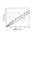
実験例1で用いた作製条件を用いて、インジウム組成の異なる井戸層を有する青色LEDチップを作製する。図9は、電流密度125A/cm2における外部量子効率のインジウム組成に関する依存性を示す図面である。図10は、電流密度12.5A/cm2における外部量子効率に対する電流密度125A/cm2における外部量子効率の比(百分率)のインジウム組成に関する依存性を示す図面である。図10を参照すると、インジウム組成が小さくなるにつれて、外部量子効率の比が大きくなる。この比の値は、インジウム組成0.14、0.11、0.10、0.09において、それぞれ、63.3%、79.0%、72.3%、82.3%である。インジウム組成0.14での値はほぼ65%であるが、インジウム組成の他の値では65%よりも大きいので、インジウム組成0.14未満の井戸層では好適な特性が得られる。外部量子効率の比65%を基準にする理由は従来の青色LEDの標準的な値だからである。
(Experimental example 8): Dependence of well layer on indium composition Using the production conditions used in Experimental example 1, a blue LED chip having well layers with different indium compositions is produced. FIG. 9 is a graph showing the dependence of the external quantum efficiency on the indium composition at a current density of 125 A / cm 2 . FIG. 10 is a drawing showing the dependence of the ratio (percentage) of the external quantum efficiency at a current density of 125 A / cm 2 on the indium composition with respect to the external quantum efficiency at a current density of 12.5 A / cm 2 . Referring to FIG. 10, the external quantum efficiency ratio increases as the indium composition decreases. The values of this ratio are 63.3%, 79.0%, 72.3%, and 82.3% at indium compositions of 0.14, 0.11, 0.10, and 0.09, respectively. The value at an indium composition of 0.14 is approximately 65%, but other values of the indium composition are greater than 65%, so that favorable characteristics can be obtained with a well layer having an indium composition of less than 0.14. The reason for setting the external quantum efficiency ratio of 65% as a standard is that it is a standard value of a conventional blue LED.
(実験例9):井戸層の厚み依存性
実験例1で用いた作製条件を用いて、厚みの異なる井戸層を有する青色LEDチップを作製する。図11は、電流密度125A/cm2における外部量子効率の井戸層の厚みに関する依存性を示す図面である。図12は、電流密度12.5A/cm2における外部量子効率に対する電流密度125A/cm2における外部量子効率の比(百分率)の井戸層の厚みに関する依存性を示す図面である。図12を参照すると、井戸層の厚みが大きくなるにつれて、外部量子効率の比が大きくなる。この比の値は、井戸層の厚み3nm、4.5nm、5nm、5.5nmにおいて、それぞれ、63.3%、79.0%、72.3%、82.3%である。井戸層の厚み3nmでの値はほぼ65%であるが、井戸層の他の厚みでは65%よりも大きいので、発明者らの他の実験の結果を勘案して井戸層の厚み4nm以上の井戸層で好適である。
Experimental Example 9: Well Layer Thickness Dependence Using the manufacturing conditions used in Experimental Example 1, blue LED chips having well layers having different thicknesses are manufactured. FIG. 11 is a diagram showing the dependence of the external quantum efficiency on the thickness of the well layer at a current density of 125 A / cm 2 . FIG. 12 is a graph showing the dependence of the ratio (percentage) of the external quantum efficiency at a current density of 125 A / cm 2 to the external quantum efficiency at a current density of 12.5 A / cm 2 on the thickness of the well layer. Referring to FIG. 12, the external quantum efficiency ratio increases as the thickness of the well layer increases. The values of this ratio are 63.3%, 79.0%, 72.3%, and 82.3% at the well layer thicknesses of 3 nm, 4.5 nm, 5 nm, and 5.5 nm, respectively. The value of the well layer thickness of 3 nm is approximately 65%, but the other thickness of the well layer is larger than 65%. Therefore, the thickness of the well layer is 4 nm or more in consideration of the results of other experiments by the inventors. A well layer is preferred.
(第2の実施の形態)
図13(A)、図13(B)、図14(A)および図14(B)は、本実施の形態に係る半導体発光素子を作製する方法を示す図面である。貫通転位密度1×107cm−2以下のn型の窒化ガリウム基板51を準備する。この窒化ガリウム基板51を有機金属気相成長炉53のサセプタ上に配置する。図13(A)に示されるようにと、有機金属気相成長炉53を用いて、窒化ガリウム基板51上にn型AlGaN膜55を成長する。AlGaN膜55上にn型窒化ガリウム系半導体膜57を成長する。窒化ガリウム系半導体膜57に先立ってAlGaN膜55を堆積すると、窒化ガリウム基板51の表面に比べて、窒化ガリウム系半導体膜57の成長に好適な表面が提供される。窒化ガリウム基板51を用いているので、窒化ガリウム系半導体膜57の貫通転位密度は1×107cm−2以下である。
(Second Embodiment)
13A, 13B, 14A, and 14B are diagrams illustrating a method for manufacturing a semiconductor light-emitting element according to this embodiment. An n-type
図13(B)に示されるように、活性領域59を窒化ガリウム系半導体膜57上に形成する。活性領域59は量子井戸構造を有しており、この量子井戸構造は、420nm以上490nm以下の波長範囲内のピーク波長を有する光を発生するように設けられている。量子井戸構造の井戸層はアンドープInXGa1−XN(0<X<0.14、Xは歪み組成)領域を含むと共に、量子井戸構造の障壁層はアンドープInYGa1−YN(0<Y<0.05、Yは歪み組成)領域を含む。井戸層の成膜温度(例えば、摂氏800度)は障壁層の成膜温度(例えば、摂氏900度)より小さい。井戸層の成膜温度は、例えば、摂氏750度以上であることが好ましく、また井戸層の成膜温度は、例えば、摂氏850度以下であることが好ましい。障壁層の成膜温度は、例えば、摂氏850度以上であることが好ましく、また障壁層の成膜温度は、例えば、摂氏950度以下であることが好ましい。
As shown in FIG. 13B, the
なお、量子井戸構造の障壁層として、アンドープInYGa1−YN(0≦Y≦0.05、Yは歪み組成)領域に替えて、n型ドーパントを含むInYGa1−YN(0≦Y≦0.05、Yは歪み組成、Y<X)領域を用いることもできる。 Incidentally, as a barrier layer for the quantum well structure, an undoped In Y Ga 1-Y N ( 0 ≦ Y ≦ 0.05, Y : strained composition) in place of the region, In containing n-type dopant Y Ga 1-Y N ( 0 ≦ Y ≦ 0.05, Y is a strain composition, and Y <X) region can also be used.
また井戸層の厚さが4nm以上であることが好ましい。また、井戸層の厚さが10nm以上であることが好ましい。 Moreover, it is preferable that the thickness of a well layer is 4 nm or more. Moreover, it is preferable that the thickness of a well layer is 10 nm or more.
この方法によれば、井戸層の成膜温度を障壁層の成膜温度より小さくすると共に井戸層のIn組成を低くすることによって、In組成ゆらぎが抑制される。井戸層のIn組成を低くすると、In組成ゆらぎに起因した局在準位の数が減少する。ところが、局在準位の減少により、活性領域は、むしろ転位の影響を強く受けるようになる。つまり、活性領域59の結晶品質は、活性領域59および下地層57の貫通転位密度に敏感になる。また、単に井戸層のIn組成を下げると、発光波長がシフトしてしまう。このシフトを防ぎ波長420nm以上490nm以下の発光を得るために、井戸層の厚みを厚くする必要がある。井戸層の厚みを厚くするとInGaN井戸層の結晶品質が低下する。下地層57の貫通転位密度1×107cm−2以下とするので、転位に敏感になることおよび井戸層を厚くすることの影響を小さくできる。このため、高電流密度での外部量子効率の低下を抑制できる。
According to this method, the In composition fluctuation is suppressed by making the deposition temperature of the well layer lower than the deposition temperature of the barrier layer and lowering the In composition of the well layer. When the In composition of the well layer is lowered, the number of localized levels due to fluctuations in the In composition is reduced. However, due to the decrease of the localized level, the active region is rather strongly influenced by the dislocation. That is, the crystal quality of the
図14(A)に示されるように、有機金属気相成長炉53を用いて、活性領域59上にp型窒化ガリウム系半導体膜61を成長する。p型窒化ガリウム系半導体膜61は、例えばGaNまたはAlGaNからなることができる。p型窒化ガリウム系半導体膜61およびn型窒化ガリウム系半導体膜57のバンドギャップエネルギは、活性領域59の井戸層のバンドギャップエネルギより大きい。このため、p型窒化ガリウム系半導体膜61およびn型窒化ガリウム系半導体膜57は、クラッド層として働く。
As shown in FIG. 14A, a p-type gallium nitride based semiconductor film 61 is grown on the
図14(B)に示されるように、有機金属気相成長炉53を用いて、p型窒化ガリウム系半導体膜61上にp型窒化ガリウム系半導体膜63を成長する。p型窒化ガリウム系半導体膜63は、例えばInGaN、GaNまたはAlGaNからなることができる。以上説明したように、本発明の実施の形態によれば、高い電流に密度においても外部量子効率の低下が小さい半導体発光素子を作製する方法が提供される。
As shown in FIG. 14B, a p-type gallium nitride based semiconductor film 63 is grown on a p-type gallium nitride based semiconductor film 61 using a metal organic vapor
好適な実施の形態において本発明の原理を図示し説明してきたが、本発明は、そのような原理から逸脱することなく配置および詳細において変更され得ることは、当業者によって認識される。本発明は、本実施の形態に開示された特定の構成に限定されるものではない。実施の形態では、基板として、GaN基板、サファイアテンプレート、SiC基板を例示したが、これらの限定されること無く、本発明は、AlN、ZrB2等も用いることができる。したがって、特許請求の範囲およびその精神の範囲から来る全ての修正および変更に権利を請求する。 While the principles of the invention have been illustrated and described in the preferred embodiments, it will be appreciated by those skilled in the art that the invention can be modified in arrangement and detail without departing from such principles. The present invention is not limited to the specific configuration disclosed in the present embodiment. In the embodiment, the GaN substrate, the sapphire template, and the SiC substrate are exemplified as the substrate. However, the present invention is not limited to these, and AlN, ZrB 2 or the like can be used. We therefore claim all modifications and changes that come within the scope and spirit of the following claims.
11、11a…半導体発光素子、13…窒化ガリウム系クラッド層、15…第2導電型の窒化ガリウム系クラッド層、17…活性領域、17a…量子井戸構造、19…井戸層、21…障壁層、23…III族窒化物基板、27…窒化ガリウム系半導体中間層、29…コンタクト層、31…第1のオーミック電極、33…第2のオーミック電極、37…活性領域、37a…量子井戸構造、39…井戸層、41…障壁層、DW…井戸層の厚み、51…窒化ガリウム基板、53…有機金属気相成長炉、55…n型AlGaN膜、57…窒化ガリウム系半導体膜、59…活性領域、61…p型窒化ガリウム系半導体膜、63…p型窒化ガリウム系半導体膜
DESCRIPTION OF
Claims (12)
第2導電型窒化ガリウム系クラッド層と、
複数の井戸層および障壁層を含む量子井戸構造を有しており前記第1導電型窒化ガリウム系クラッド層と前記第2導電型窒化ガリウム系クラッド層との間に設けられた活性領域と
を備え、
前記活性領域は前記第1導電型窒化ガリウム系クラッド層上に形成され、前記活性領域の前記井戸層および前記障壁層は交互に成長され、
前記量子井戸構造は、420nm以上490nm以下の波長範囲内のピーク波長を有する光を発生するように設けられており、
前記井戸層の各々は、アンドープInXGa1−XN(0<X<0.14、Xは歪み組成)領域を含み、
前記井戸層の厚さが4nm以上であり、
前記井戸層の厚さが10nm以下であり、
前記障壁層は、アンドープInYGa1−YN(0≦Y≦0.05、Yは歪み組成、Y<X)領域を含む、ことを特徴とする半導体発光素子。 A first conductivity type gallium nitride cladding layer having a threading dislocation density of 1 × 10 7 cm −2 or less;
A second conductivity type gallium nitride cladding layer;
An active region having a quantum well structure including a plurality of well layers and barrier layers and provided between the first conductivity type gallium nitride cladding layer and the second conductivity type gallium nitride cladding layer; ,
The active region is formed on the first conductivity type gallium nitride based cladding layer, and the well layer and the barrier layer of the active region are alternately grown,
The quantum well structure is provided so as to generate light having a peak wavelength within a wavelength range of 420 nm or more and 490 nm or less,
Each of the well layers includes an undoped In X Ga 1-X N (0 <X <0.14, X is a strain composition) region,
The well layer has a thickness of 4 nm or more;
The well layer has a thickness of 10 nm or less;
The semiconductor light emitting element, wherein the barrier layer includes an undoped In Y Ga 1-Y N (0 ≦ Y ≦ 0.05, Y is a strain composition, Y <X) region.
第2導電型窒化ガリウム系クラッド層と、
複数の井戸層および障壁層を含む量子井戸構造を有しており前記第1導電型窒化ガリウム系クラッド層と前記第2導電型窒化ガリウム系クラッド層との間に設けられた活性領域と
を備え、
前記活性領域は前記第1導電型窒化ガリウム系クラッド層上に形成され、前記活性領域の前記井戸層および前記障壁層は交互に成長され、
前記量子井戸構造は、波長420nm以上490nm以下の波長範囲内のピーク波長を有する光を発生するように設けられており、
前記井戸層の各々は、アンドープInXGa1−XN(0<X<0.14、Xは歪み組成)領域を含み、
前記井戸層の厚さが4nm以上であり、
前記井戸層の厚さが10nm以下であり、
前記障壁層は、n型ドーパントを含むInYGa1−YN(0≦Y≦0.05、Yは歪み組成、Y<X)領域を含む、ことを特徴とする半導体発光素子。 A first conductivity type gallium nitride cladding layer having a threading dislocation density of 1 × 10 7 cm −2 or less;
A second conductivity type gallium nitride cladding layer;
An active region having a quantum well structure including a plurality of well layers and barrier layers and provided between the first conductivity type gallium nitride cladding layer and the second conductivity type gallium nitride cladding layer; ,
The active region is formed on the first conductivity type gallium nitride based cladding layer, and the well layer and the barrier layer of the active region are alternately grown,
The quantum well structure is provided so as to generate light having a peak wavelength within a wavelength range of 420 nm or more and 490 nm or less,
Each of the well layers includes an undoped In X Ga 1-X N (0 <X <0.14, X is a strain composition) region,
The well layer has a thickness of 4 nm or more;
The well layer has a thickness of 10 nm or less;
The semiconductor light emitting element, wherein the barrier layer includes an In Y Ga 1-Y N (0 ≦ Y ≦ 0.05, Y is strain composition, Y <X) region including an n-type dopant.
前記コンタクト層上に設けられたオーミック電極と
を更に備える、ことを特徴とする請求項1または請求項2に記載された半導体発光素子。 A second conductivity type contact layer provided on the second conductivity type gallium nitride cladding layer;
The semiconductor light emitting device according to claim 1, further comprising an ohmic electrode provided on the contact layer.
前記III族窒化物基板の前記裏面に設けられた別のオーミック電極と
を更に備え、
前記第1導電型窒化ガリウム系クラッド層、前記活性領域および前記第2導電型窒化ガリウム系クラッド層を含む半導体領域は、前記III族窒化物基板の前記主面上に設けられている、ことを特徴とする請求項1〜請求項3のいずれか一項に記載された半導体発光素子。 A group III nitride substrate having a main surface and a back surface;
Further comprising another ohmic electrode provided on the back surface of the group III nitride substrate,
The semiconductor region including the first conductivity type gallium nitride cladding layer, the active region, and the second conductivity type gallium nitride cladding layer is provided on the main surface of the group III nitride substrate. The semiconductor light-emitting device according to claim 1, wherein the semiconductor light-emitting device is characterized in that:
貫通転位密度1×10 7 cm −2 以下の第1導電型の窒化ガリウム系クラッド領域をIII族窒化物基板上に成長する工程と、
420nm以上490nm以下の波長範囲内のピーク波長を有する光を発生するように設けられた量子井戸構造を有する活性領域を前記窒化ガリウム系クラッド領域上に形成する工程と、
前記活性領域上に第2導電型の別の窒化ガリウム系クラッド領域を形成する工程と、
を備え、
前記量子井戸構造は複数の井戸層および障壁層を含み、
前記活性領域の前記井戸層および前記障壁層は前記窒化ガリウム系クラッド領域上に交互に成長され、
前記井戸層の成膜温度は前記障壁層の成膜温度より小さく、
前記量子井戸構造の井戸層はアンドープInXGa1−XN(0<X<0.14、Xは歪み組成)領域を含み、
前記井戸層の厚さが4nm以上であり、
前記井戸層の厚さが10nm以下であり、
前記量子井戸構造の障壁層はアンドープInYGa1−YN(0≦Y≦0.05、Yは歪み組成)領域を含む、ことを特徴とする方法。 A method for producing a semiconductor light emitting device, comprising:
Growing a first conductivity type gallium nitride cladding region having a threading dislocation density of 1 × 10 7 cm −2 or less on a group III nitride substrate;
Forming an active region on the gallium nitride-based cladding region having a quantum well structure provided so as to emit light having a peak wavelength in 490nm or less in the wavelength range of 420 nm,
Forming another gallium nitride based cladding region of the second conductivity type on the active region;
With
The quantum well structure includes a plurality of well layers and barrier layers;
The well layer and the barrier layer of the active region are alternately grown on the gallium nitride based cladding region,
The deposition temperature of the well layer is smaller than the deposition temperature of the barrier layer,
The well layer of the quantum well structure includes an undoped In X Ga 1-X N (0 <X <0.14, X is a strain composition) region,
The well layer has a thickness of 4 nm or more;
The well layer has a thickness of 10 nm or less;
The barrier layer of the quantum well structure includes an undoped In Y Ga 1-Y N (0 ≦ Y ≦ 0.05, Y is strain composition) region.
貫通転位密度1×10 7 cm −2 以下の第1導電型の窒化ガリウム系クラッド領域をIII族窒化物基板上に成長する工程と、
420nm以上490nm以下の波長範囲内のピーク波長を有する光を発生するように設けられた量子井戸構造を有する活性領域を前記窒化ガリウム系クラッド領域上に形成する工程と、
前記活性領域上に第2導電型の別の窒化ガリウム系クラッド領域を形成する工程と、
を備え、
前記量子井戸構造は複数の井戸層および障壁層を含み、
前記活性領域の前記井戸層および前記障壁層は前記窒化ガリウム系クラッド領域上に交互に成長され、
前記井戸層の成膜温度は前記障壁層の成膜温度より小さく、
前記量子井戸構造の井戸層はアンドープInXGa1−XN(0<X<0.14、Xは歪み組成)領域を含み、
前記井戸層の厚さが4nm以上であり、
前記井戸層の厚さが10nm以下であり、
前記量子井戸構造の障壁層はn型ドーパントを含むInYGa1−YN(0≦Y≦0.05、Yは歪み組成)領域を含む、ことを特徴とする方法。 A method for producing a semiconductor light emitting device, comprising:
Growing a first conductivity type gallium nitride cladding region having a threading dislocation density of 1 × 10 7 cm −2 or less on a group III nitride substrate;
Forming an active region on the gallium nitride-based cladding region having a quantum well structure provided so as to emit light having a peak wavelength in 490nm or less in the wavelength range of 420 nm,
Forming another gallium nitride based cladding region of the second conductivity type on the active region;
With
The quantum well structure includes a plurality of well layers and barrier layers;
The well layer and the barrier layer of the active region are alternately grown on the gallium nitride based cladding region,
The deposition temperature of the well layer is smaller than the deposition temperature of the barrier layer,
The well layer of the quantum well structure includes an undoped In X Ga 1-X N (0 <X <0.14, X is a strain composition) region,
The well layer has a thickness of 4 nm or more;
The well layer has a thickness of 10 nm or less;
The quantum well structure barrier layer includes an In Y Ga 1-Y N (0 ≦ Y ≦ 0.05, Y is strain composition) region including an n-type dopant.
Priority Applications (2)
| Application Number | Priority Date | Filing Date | Title |
|---|---|---|---|
| JP2005326270A JP5048236B2 (en) | 2005-11-10 | 2005-11-10 | Semiconductor light emitting device and method for manufacturing semiconductor light emitting device |
| US11/863,220 US7547910B2 (en) | 2005-11-10 | 2007-09-27 | Semiconductor light-emitting device and method of manufacturing semiconductor light-emitting device |
Applications Claiming Priority (1)
| Application Number | Priority Date | Filing Date | Title |
|---|---|---|---|
| JP2005326270A JP5048236B2 (en) | 2005-11-10 | 2005-11-10 | Semiconductor light emitting device and method for manufacturing semiconductor light emitting device |
Related Child Applications (1)
| Application Number | Title | Priority Date | Filing Date |
|---|---|---|---|
| JP2011173949A Division JP2011223043A (en) | 2011-08-09 | 2011-08-09 | Semiconductor light-emitting device and method of manufacturing the semiconductor light-emitting device |
Publications (2)
| Publication Number | Publication Date |
|---|---|
| JP2007134507A JP2007134507A (en) | 2007-05-31 |
| JP5048236B2 true JP5048236B2 (en) | 2012-10-17 |
Family
ID=38155917
Family Applications (1)
| Application Number | Title | Priority Date | Filing Date |
|---|---|---|---|
| JP2005326270A Expired - Fee Related JP5048236B2 (en) | 2005-11-10 | 2005-11-10 | Semiconductor light emitting device and method for manufacturing semiconductor light emitting device |
Country Status (2)
| Country | Link |
|---|---|
| US (1) | US7547910B2 (en) |
| JP (1) | JP5048236B2 (en) |
Families Citing this family (16)
| Publication number | Priority date | Publication date | Assignee | Title |
|---|---|---|---|---|
| KR100818269B1 (en) * | 2006-06-23 | 2008-04-01 | 삼성전자주식회사 | Nitride Based Compound Semiconductor Light Emitting Device |
| JP5003527B2 (en) * | 2008-02-22 | 2012-08-15 | 住友電気工業株式会社 | Group III nitride light emitting device and method for fabricating group III nitride semiconductor light emitting device |
| JP5077303B2 (en) * | 2008-10-07 | 2012-11-21 | 住友電気工業株式会社 | Gallium nitride based semiconductor light emitting device, method for fabricating gallium nitride based semiconductor light emitting device, gallium nitride based light emitting diode, epitaxial wafer, and method for fabricating gallium nitride based light emitting diode |
| JP2010118647A (en) * | 2008-10-17 | 2010-05-27 | Sumitomo Electric Ind Ltd | Nitride-based semiconductor light emitting element, method of manufacturing nitride-based semiconductor light emitting element, and light emitting device |
| JP5234022B2 (en) * | 2009-07-15 | 2013-07-10 | 住友電気工業株式会社 | Nitride semiconductor light emitting device |
| US8502465B2 (en) * | 2009-09-18 | 2013-08-06 | Soraa, Inc. | Power light emitting diode and method with current density operation |
| US9583678B2 (en) | 2009-09-18 | 2017-02-28 | Soraa, Inc. | High-performance LED fabrication |
| US9293644B2 (en) | 2009-09-18 | 2016-03-22 | Soraa, Inc. | Power light emitting diode and method with uniform current density operation |
| TWI560963B (en) * | 2010-03-04 | 2016-12-01 | Univ California | Semi-polar iii-nitride optoelectronic devices on m-plane substrates with miscuts less than +/- 15 degrees in the c-direction |
| JP5388967B2 (en) * | 2010-08-09 | 2014-01-15 | 株式会社東芝 | Semiconductor light emitting device |
| JP2012243780A (en) * | 2011-05-13 | 2012-12-10 | Toshiba Corp | Semiconductor light-emitting element and wafer |
| JP2012244154A (en) * | 2012-01-23 | 2012-12-10 | Toshiba Corp | Semiconductor light-emitting element and wafer |
| JP2012109624A (en) * | 2012-03-06 | 2012-06-07 | Sumitomo Electric Ind Ltd | Group iii nitride light-emitting element and method of manufacturing group iii nitride-based semiconductor light-emitting element |
| US20130299776A1 (en) * | 2012-05-09 | 2013-11-14 | The Regents Of The University Of California | High output power, high efficiency blue light-emitting diodes |
| US20130299777A1 (en) * | 2012-05-09 | 2013-11-14 | The Regents Of The University Of California | Light-emitting diodes with low temperature dependence |
| CN116825917B (en) * | 2023-08-31 | 2023-11-17 | 江西兆驰半导体有限公司 | Light-emitting diode epitaxial wafer, preparation method thereof and light-emitting diode |
Family Cites Families (9)
| Publication number | Priority date | Publication date | Assignee | Title |
|---|---|---|---|---|
| JP2932467B2 (en) | 1993-03-12 | 1999-08-09 | 日亜化学工業株式会社 | Gallium nitride based compound semiconductor light emitting device |
| JP2780691B2 (en) | 1994-12-02 | 1998-07-30 | 日亜化学工業株式会社 | Nitride semiconductor light emitting device |
| JP3835225B2 (en) * | 1995-02-23 | 2006-10-18 | 日亜化学工業株式会社 | Nitride semiconductor light emitting device |
| JP3905935B2 (en) * | 1995-09-01 | 2007-04-18 | 株式会社東芝 | Semiconductor device and method for manufacturing semiconductor device |
| AU747260B2 (en) * | 1997-07-25 | 2002-05-09 | Nichia Chemical Industries, Ltd. | Nitride semiconductor device |
| JP2000133883A (en) * | 1998-10-22 | 2000-05-12 | Nichia Chem Ind Ltd | Nitride semiconductor element |
| JP4416297B2 (en) * | 2000-09-08 | 2010-02-17 | シャープ株式会社 | Nitride semiconductor light emitting element, and light emitting device and optical pickup device using the same |
| JP2003183099A (en) * | 2001-12-18 | 2003-07-03 | Sanyo Electric Co Ltd | Method and apparatus for producing single crystal |
| JP4307113B2 (en) * | 2002-03-19 | 2009-08-05 | 宣彦 澤木 | Semiconductor light emitting device and manufacturing method thereof |
-
2005
- 2005-11-10 JP JP2005326270A patent/JP5048236B2/en not_active Expired - Fee Related
-
2007
- 2007-09-27 US US11/863,220 patent/US7547910B2/en not_active Expired - Fee Related
Also Published As
| Publication number | Publication date |
|---|---|
| US20080023708A1 (en) | 2008-01-31 |
| US7547910B2 (en) | 2009-06-16 |
| JP2007134507A (en) | 2007-05-31 |
Similar Documents
| Publication | Publication Date | Title |
|---|---|---|
| JP5048236B2 (en) | Semiconductor light emitting device and method for manufacturing semiconductor light emitting device | |
| JP4572963B2 (en) | Group III nitride semiconductor light emitting device and epitaxial wafer | |
| JP4539752B2 (en) | Method for forming quantum well structure and method for manufacturing semiconductor light emitting device | |
| JP5050574B2 (en) | Group III nitride semiconductor light emitting device | |
| JP5634368B2 (en) | Semiconductor device | |
| JPWO2008153130A1 (en) | Nitride semiconductor light emitting device and method for manufacturing nitride semiconductor | |
| JP2008258503A (en) | Nitride-based semiconductor light emitting element, and method of fabricating nitride-based semiconductor light emitting element | |
| JP5279006B2 (en) | Nitride semiconductor light emitting device | |
| US20140209013A1 (en) | Crystal growth method for nitride semiconductor having a multiquantum well structure | |
| JP2006332258A (en) | Nitride semiconductor device and its manufacturing method | |
| JP3269344B2 (en) | Crystal growth method and semiconductor light emitting device | |
| JP2008118049A (en) | GaN-BASED SEMICONDUCTOR LIGHT EMITTING DEVICE | |
| JP4940670B2 (en) | Method for fabricating nitride semiconductor light emitting device | |
| JP2009245982A (en) | Nitride light-emitting element | |
| JP2009231609A (en) | Production method of semiconductor light-emitting element | |
| JP2008118048A (en) | GaN-BASED SEMICONDUCTOR LIGHT EMITTING DEVICE | |
| JP3753369B2 (en) | Nitride semiconductor light emitting device | |
| JP4900336B2 (en) | Method for manufacturing group III nitride light emitting device, and group III nitride light emitting device | |
| JP2011223043A (en) | Semiconductor light-emitting device and method of manufacturing the semiconductor light-emitting device | |
| JP2008227103A (en) | GaN-BASED SEMICONDUCTOR LIGHT EMITTING ELEMENT | |
| JP7319559B2 (en) | Nitride semiconductor light emitting device | |
| JP6071044B2 (en) | Semiconductor light emitting device and manufacturing method thereof | |
| JP3767534B2 (en) | Light emitting device | |
| JP2009026956A (en) | Light emitting device, substrate product for light emitting device, and method of fabricating light emitting device | |
| JP4369970B2 (en) | Method for manufacturing compound semiconductor light emitting device and compound semiconductor light emitting device |
Legal Events
| Date | Code | Title | Description |
|---|---|---|---|
| A621 | Written request for application examination |
Free format text: JAPANESE INTERMEDIATE CODE: A621 Effective date: 20070822 |
|
| A977 | Report on retrieval |
Free format text: JAPANESE INTERMEDIATE CODE: A971007 Effective date: 20100608 |
|
| A131 | Notification of reasons for refusal |
Free format text: JAPANESE INTERMEDIATE CODE: A131 Effective date: 20100615 |
|
| A521 | Request for written amendment filed |
Free format text: JAPANESE INTERMEDIATE CODE: A523 Effective date: 20100816 |
|
| A02 | Decision of refusal |
Free format text: JAPANESE INTERMEDIATE CODE: A02 Effective date: 20110510 |
|
| A521 | Request for written amendment filed |
Free format text: JAPANESE INTERMEDIATE CODE: A523 Effective date: 20110809 |
|
| A911 | Transfer to examiner for re-examination before appeal (zenchi) |
Free format text: JAPANESE INTERMEDIATE CODE: A911 Effective date: 20110815 |
|
| A912 | Re-examination (zenchi) completed and case transferred to appeal board |
Free format text: JAPANESE INTERMEDIATE CODE: A912 Effective date: 20120224 |
|
| A01 | Written decision to grant a patent or to grant a registration (utility model) |
Free format text: JAPANESE INTERMEDIATE CODE: A01 |
|
| A61 | First payment of annual fees (during grant procedure) |
Free format text: JAPANESE INTERMEDIATE CODE: A61 Effective date: 20120719 |
|
| FPAY | Renewal fee payment (event date is renewal date of database) |
Free format text: PAYMENT UNTIL: 20150727 Year of fee payment: 3 |
|
| R150 | Certificate of patent or registration of utility model |
Ref document number: 5048236 Country of ref document: JP Free format text: JAPANESE INTERMEDIATE CODE: R150 Free format text: JAPANESE INTERMEDIATE CODE: R150 |
|
| R250 | Receipt of annual fees |
Free format text: JAPANESE INTERMEDIATE CODE: R250 |
|
| R250 | Receipt of annual fees |
Free format text: JAPANESE INTERMEDIATE CODE: R250 |
|
| R250 | Receipt of annual fees |
Free format text: JAPANESE INTERMEDIATE CODE: R250 |
|
| R250 | Receipt of annual fees |
Free format text: JAPANESE INTERMEDIATE CODE: R250 |
|
| R250 | Receipt of annual fees |
Free format text: JAPANESE INTERMEDIATE CODE: R250 |
|
| R250 | Receipt of annual fees |
Free format text: JAPANESE INTERMEDIATE CODE: R250 |
|
| R250 | Receipt of annual fees |
Free format text: JAPANESE INTERMEDIATE CODE: R250 |
|
| LAPS | Cancellation because of no payment of annual fees |