JP7319559B2 - Nitride semiconductor light emitting device - Google Patents
Nitride semiconductor light emitting device Download PDFInfo
- Publication number
- JP7319559B2 JP7319559B2 JP2021141352A JP2021141352A JP7319559B2 JP 7319559 B2 JP7319559 B2 JP 7319559B2 JP 2021141352 A JP2021141352 A JP 2021141352A JP 2021141352 A JP2021141352 A JP 2021141352A JP 7319559 B2 JP7319559 B2 JP 7319559B2
- Authority
- JP
- Japan
- Prior art keywords
- layer
- well
- nitride semiconductor
- well layer
- barrier
- Prior art date
- Legal status (The legal status is an assumption and is not a legal conclusion. Google has not performed a legal analysis and makes no representation as to the accuracy of the status listed.)
- Active
Links
Images


Description
本開示に係る発明は、窒化物半導体発光素子に関する。 The invention according to the present disclosure relates to a nitride semiconductor light emitting device.
従来から、井戸層と障壁層とが交互に積層された多重量子井戸構造の活性層を備えた窒化物発光素子が知られている。特に、特許文献1~3には、複数の井戸層の膜厚が互いに異なる層構造が開示されている。また、特許文献4(特に、段落[0078])には、p型窒化物半導体層の成長時の熱拡散により、多重量子井戸発光層の全ての障壁層にp型不純物がドープされる可能性がある点について記載されている。 2. Description of the Related Art Nitride light-emitting devices having an active layer having a multiple quantum well structure in which well layers and barrier layers are alternately laminated have been conventionally known. In particular, Patent Documents 1 to 3 disclose layer structures in which a plurality of well layers have different film thicknesses. Further, in Patent Document 4 (particularly, paragraph [0078]), there is a possibility that all the barrier layers of the multiple quantum well light emitting layer are doped with p-type impurities due to thermal diffusion during the growth of the p-type nitride semiconductor layer. is described on a certain point.
上述の窒化物発光素子の発光効率は、十分とは言い難く、発光効率の更なる向上が求められている。そこで、本開示は、さらなる発光効率の向上を図った窒化物半導体発光素子を提供することを目的とする。 It is difficult to say that the luminous efficiency of the nitride light-emitting device described above is sufficient, and further improvement in luminous efficiency is desired. Accordingly, an object of the present disclosure is to provide a nitride semiconductor light-emitting device with further improved luminous efficiency.
以上の目的を達成するために、本開示に係る窒化物半導体発光素子は、
n側窒化物半導体層と、p側窒化物半導体層と、n側窒化物半導体層とp側窒化物半導体層との間に設けられ、井戸層と障壁層とからなる複数の積層部を含む活性層と、を含み、
複数の前記井戸層は、前記n側窒化物半導体層側から順に、第1井戸層と、第2井戸層と、複数の前記井戸層のうち最も前記p側窒化物半導体層の近くに位置する第3井戸層と、を含み、
前記第2井戸層の膜厚は、前記第1井戸層の膜厚よりも厚く、
前記第3井戸層の膜厚は、前記第2井戸層の膜厚よりも厚く、
複数の前記障壁層のうち前記第3井戸層と前記p側窒化物半導体層との間に位置する第1障壁層には、p型不純物がドープされている。
In order to achieve the above objects, the nitride semiconductor light emitting device according to the present disclosure includes
n-side nitride semiconductor layer, p-side nitride semiconductor layer, and a plurality of lamination portions provided between the n-side nitride semiconductor layer and the p-side nitride semiconductor layer and composed of well layers and barrier layers an active layer;
The plurality of well layers are positioned closest to the p-side nitride semiconductor layer among the first well layer, the second well layer, and the plurality of well layers in order from the n-side nitride semiconductor layer side. a third well layer;
The film thickness of the second well layer is thicker than the film thickness of the first well layer,
The film thickness of the third well layer is thicker than the film thickness of the second well layer,
A first barrier layer positioned between the third well layer and the p-side nitride semiconductor layer among the plurality of barrier layers is doped with a p-type impurity.
以上のように構成された本開示に係る窒化物半導体発光素子によれば、発光効率の向上を図ることができる。 According to the nitride semiconductor light emitting device according to the present disclosure configured as described above, it is possible to improve the luminous efficiency.
一般に、井戸層と障壁層とが交互に積層された多重量子井戸構造の活性層を含む半導体発光素子は、複数の井戸層全体を効率よく発光させることにより発光効率を高くできると考えられている。しかしながら、電子はn側窒化物半導体層から供給され、ホールはp側窒化物半導体層から供給されることから、複数の井戸層全てに偏りなく電子またはホールを供給することは必ずしも容易ではない。特に、窒化物半導体層を含む窒化物半導体発光素子においては、p側窒化物半導体層から活性層に含まれる全ての井戸層にホールを効率よく供給することは容易ではなく、p側窒化物半導体層側に位置する井戸層にホールの供給が偏りやすい傾向がある。これにより、特に、窒化物半導体発光素子においては、n側窒化物半導体層側に位置する井戸層にホールが供給されにくく、n側窒化物半導体層側に位置する井戸層の発光効率を高くすることが難しいという課題がある。 In general, it is believed that a semiconductor light-emitting device including an active layer having a multi-quantum well structure in which well layers and barrier layers are alternately laminated can increase the luminous efficiency by allowing the entire plurality of well layers to emit light efficiently. . However, since electrons are supplied from the n-side nitride semiconductor layer and holes are supplied from the p-side nitride semiconductor layer, it is not necessarily easy to evenly supply electrons or holes to all of the plurality of well layers. In particular, in a nitride semiconductor light emitting device including a nitride semiconductor layer, it is not easy to efficiently supply holes from the p-side nitride semiconductor layer to all the well layers included in the active layer. Holes tend to be supplied unevenly to the well layer located on the layer side. As a result, particularly in the nitride semiconductor light emitting device, holes are less likely to be supplied to the well layer located on the n-side nitride semiconductor layer side, and the luminous efficiency of the well layer located on the n-side nitride semiconductor layer side is increased. There is a problem that it is difficult to
本開示に係る発明は、上記知見に基づき鋭意検討した結果なされたものであり、活性層に含まれる全ての井戸層を発光させようとするのではなく、活性層全体として発光効率を高めようとする発明である。 The invention according to the present disclosure has been made as a result of intensive studies based on the above knowledge, and aims to increase the luminous efficiency of the entire active layer instead of making all the well layers included in the active layer emit light. It is an invention to
具体的には、複数の井戸層のうち、n側窒化物半導体層側に位置する第1井戸層は、ホールが供給されにくく発光にほとんど寄与しないことから、第1井戸層での発光は抑えてp側窒化物半導体層側の井戸層により多くの電子を供給させられるようにすることが好ましい。このことから、第1井戸層の膜厚をp側窒化物半導体層側に位置する井戸層の膜厚より薄くすることで、第1井戸層よりもp側窒化物半導体層側に位置する井戸層に電子が供給されやすくしている。このように、第1井戸層は、第1井戸層よりもp側窒化物半導体層側の井戸層を効率よく発光させることに寄与し、結果として、順方向電圧の低い窒化物半導体発光素子の提供を可能としている。 Specifically, among the plurality of well layers, the first well layer located on the n-side nitride semiconductor layer side is less likely to be supplied with holes and hardly contributes to light emission, so light emission in the first well layer is suppressed. It is preferable to supply more electrons to the well layer on the p-side nitride semiconductor layer side. Therefore, by making the film thickness of the first well layer thinner than the film thickness of the well layer located on the p-side nitride semiconductor layer side, the well layer located on the p-side nitride semiconductor layer side than the first well layer It makes it easier for electrons to be supplied to the layer. Thus, the first well layer contributes to efficient light emission from the well layer closer to the p-side nitride semiconductor layer than the first well layer, resulting in a nitride semiconductor light emitting device having a low forward voltage. making it possible to provide.
また、最もp側窒化物半導体層側に位置する第3井戸層は、p側窒化物半導体層からホールが供給されやすく、第1井戸層を介して供給された電子とp側窒化物半導体層から供給されるホールとが再結合され、複数の井戸層のうち主に発光に寄与する井戸層である。そのため、第3井戸層においてより効率よく発光再結合が行われるように、第3井戸層の膜厚を第1井戸層を含む他の井戸層の膜厚より厚くしている。 Further, the third well layer located closest to the p-side nitride semiconductor layer is easily supplied with holes from the p-side nitride semiconductor layer, and the electrons supplied through the first well layer and the p-side nitride semiconductor layer It is a well layer that mainly contributes to light emission among a plurality of well layers by recombination with holes supplied from . Therefore, the film thickness of the third well layer is made thicker than the film thickness of the other well layers including the first well layer so that radiative recombination is performed more efficiently in the third well layer.
第2井戸層は、第1井戸層よりも厚く、第3井戸層よりも薄い膜厚で構成されており、発光に寄与するとともに結晶性の悪化を低減するための層である。第2井戸層を設けることなく、第2井戸層よりも薄い第1井戸層の膜厚から第2井戸層よりも厚い第3井戸層に膜厚に変化させて井戸層を成長させると井戸層の結晶性が悪化する傾向がある。この発明者の知見に基づき、第1井戸層と第3井戸層の間に、第1井戸層よりも厚く、第3井戸層よりも薄い膜厚の第2井戸層を設けることで第3井戸層の結晶性の悪化を低減することができる。 The second well layer is thicker than the first well layer and thinner than the third well layer, and is a layer that contributes to light emission and reduces deterioration of crystallinity. If the thickness of the well layer is changed from the first well layer thinner than the second well layer to the third well layer thicker than the second well layer without providing the second well layer, the well layer is grown. crystallinity tends to deteriorate. Based on the findings of the inventor, a second well layer having a thickness thicker than the first well layer and thinner than the third well layer is provided between the first well layer and the third well layer. Deterioration of crystallinity of the layer can be reduced.
また、複数の障壁層のうち第3井戸層とp側窒化物半導体層との間に位置する第1障壁層は、第3井戸層または第2井戸層に効率よくホールを注入するためにp型不純物がドープされている。 Further, among the plurality of barrier layers, the first barrier layer positioned between the third well layer and the p-side nitride semiconductor layer has a p-layer structure for efficiently injecting holes into the third well layer or the second well layer. are doped with type impurities.
以上のように構成された窒化物半導体発光素子は、上述したように、活性層に含まれる第1井戸層、第2井戸層、及び第3井戸層の膜厚を異ならせ、かつ複数の障壁層のうち第3井戸層とp側窒化物半導体層との間に位置する第1障壁層にp型不純物をドープすることで、発光効率を向上させることができる。 In the nitride semiconductor light emitting device configured as described above, the thicknesses of the first well layer, the second well layer, and the third well layer included in the active layer are varied, and the plurality of barrier layers are formed. By doping the first barrier layer, which is located between the third well layer and the p-side nitride semiconductor layer, with a p-type impurity, the luminous efficiency can be improved.
以下、より具体的な形態について詳細に説明する。なお、後述する本実施形態の窒化物半導体発光素子において、窒化物半導体としては、III-V族窒化物半導体(InXAlYGa1-X-YN(0≦X、0≦Y、X+Y≦1))が挙げられる。なお、III族元素の一部にBを用いてよく、V族元素のNの一部をP、As、Sbで置換した混晶であってもよい。これらの窒化物半導体層は、例えば、有機金属気相成長法(MOCVD)、ハイドライド気相成長法(HVPE)、分子線エピタキシャル成長法(MBE)等により形成することができる。 More specific embodiments will be described in detail below. In the nitride semiconductor light-emitting device of this embodiment, which will be described later, the nitride semiconductor may be a group III-V nitride semiconductor (In X Al Y Ga 1-XY N (0≦X, 0≦Y, X+Y≦1 )). B may be used as part of the group III element, and a mixed crystal in which part of N of the group V element is substituted with P, As, or Sb may be used. These nitride semiconductor layers can be formed by, for example, metal organic chemical vapor deposition (MOCVD), hydride vapor phase epitaxy (HVPE), molecular beam epitaxy (MBE), and the like.
また、本実施形態の窒化物半導体発光素子として、活性層にInを比較的多く含む井戸層を備えた発光ピーク波長が500nm以上の窒化物半導体発光素子を例示して説明する。例えば、InaGa1-aNで構成され、In組成比aが20~28である井戸層を含み、緑色に発光する窒化物半導体発光素子である。なお、発光ピーク波長は、上記波長に限定されるものではない。また、本明細書において、数字を用いてA~Bと記載するときは、数がAである場合と数がBである場合とを含むものとする。また、本明細書において、アンドープの半導体層とは、導電性を制御するための不純物を意図的にドープするための原料ガス(例えばSiやMgを含むガス)を用いることなく形成された層であり、プロセス上不可避的に混入される不純物を含む場合もある。アンドープの半導体層のn型不純物濃度は、例えば、1×10¹⁷/cm3以下である。 As the nitride semiconductor light emitting device of the present embodiment, a nitride semiconductor light emitting device having a well layer containing a relatively large amount of In in the active layer and having an emission peak wavelength of 500 nm or more will be described as an example. For example, it is a nitride semiconductor light-emitting device that includes a well layer made of In a Ga 1-a N and having an In composition ratio a of 20 to 28, and emits green light. Note that the emission peak wavelength is not limited to the above wavelengths. In addition, in this specification, when A to B are described using numbers, the case where the number is A and the case where the number is B are included. In this specification, an undoped semiconductor layer is a layer formed without using a raw material gas (for example, a gas containing Si or Mg) for intentionally doping impurities for controlling conductivity. and may contain impurities that are unavoidably mixed in the process. The n-type impurity concentration of the undoped semiconductor layer is, for example, 1×10 17 /cm 3 or less.
<<第1実施形態>>
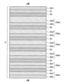
以下、図1および図2を参照しながら本開示に係る第1実施形態の窒化物半導体発光素子について説明する。本実施形態に係る窒化物半導体発光素子100は、基板1と、基板1上に設けられたn側窒化物半導体層10と、p側窒化物半導体層20と、n側窒化物半導体層10とp側窒化物半導体層20との間に位置する活性層5と、を含む。最初に本開示の窒化物半導体発光素子における活性層5について説明し、その後、基板1、n側窒化物半導体層10およびp側窒化物半導体層20の順に詳述する。
<<First Embodiment>>
A nitride semiconductor light emitting device according to a first embodiment of the present disclosure will be described below with reference to FIGS. 1 and 2. FIG. A nitride semiconductor
(活性層5)
活性層5は、井戸層と障壁層とを含む複数の積層部5bwを含んでいる。図2の形態では、n側窒化物半導体層10側から順に、障壁層と、井戸層とが積層された積層部5bwを3つ備えた積層構造を例示している。
(Active layer 5)
The
井戸層は、一例として、Inを含む窒化物半導体を用いてよく、In組成比を適宜設定することにより、青色や緑色の発光が可能である。例えば、InXAlYGa1-X-YN(0≦X、0≦Y、X+Y≦1)を用いた場合、In組成比xを所望の値とすることにより、窒化物半導体発光素子の発光ピーク波長が430nm~570nmの範囲、好ましくは500nm~570nmの範囲とすることができる。 As an example, the well layer may use a nitride semiconductor containing In, and by appropriately setting the In composition ratio, it is possible to emit blue or green light. For example, when In X Al Y Ga 1-XY N (0≦X, 0≦Y, X+Y≦1) is used, by setting the In composition ratio x to a desired value, the nitride semiconductor light emitting device can be manufactured. The emission peak wavelength can be in the range of 430 nm to 570 nm, preferably in the range of 500 nm to 570 nm.
図2に示すように、活性層5における井戸層は、n側窒化物半導体層10側から順に、第1井戸層5w1と、第2井戸層5w2と、複数の井戸層のうち最もp側窒化物半導体層20の近くに位置する第3井戸層5w3と、を含んでいる。なお、第1井戸層5w1、第2井戸層5w2および第3井戸層5w3に用いるInGaNの分解を低減するため、各井戸層の上に第1中間層5cを積層してもよい。第1中間層5cには、例えば、アンドープのGaN層を用いることができる。
As shown in FIG. 2, the well layers in the
第1井戸層5w1の膜厚は、上述したように、第1井戸層5w1よりもp側窒化物半導体層20側に位置する井戸層より薄くしている。このような構成とすることで、p側窒化物半導体層20側の井戸層により多くの電子を供給することができ、順方向電圧の低い窒化物半導体発光素子の提供を可能としている。第1井戸層5w1の膜厚は、例えば、0.5nm~4.0nmの範囲、好ましくは、1.0nm~2.5nmの範囲、より好ましくは、1.2nm~1.9nmの範囲とすることができる。第1井戸層5w1の膜厚は、他の井戸層、具体的には、第2井戸層5w2及び第3井戸層5w3との関係を考慮して設定される。
As described above, the film thickness of the first well layer 5w1 is made thinner than the well layers located closer to the p-side
第2井戸層5w2は、第1井戸層5w1よりも厚く、第3井戸層5w3よりも薄い膜厚で構成されており、発光に寄与するとともに結晶性の悪化を低減するための層である。第2井戸層5w2の膜厚は、例えば、1.5nm~5.0nmの範囲、好ましくは、2.0nm~3.5nmの範囲、より好ましくは、2.5nm~3.2nmの範囲とすることができる。第2井戸層5w2の膜厚は、他の井戸層、具体的には、第1井戸層5w1及び第3井戸層5w3との関係を考慮して設定される。 The second well layer 5w2 is thicker than the first well layer 5w1 and thinner than the third well layer 5w3, and contributes to light emission and reduces deterioration of crystallinity. The film thickness of the second well layer 5w2 is, for example, in the range of 1.5 nm to 5.0 nm, preferably in the range of 2.0 nm to 3.5 nm, more preferably in the range of 2.5 nm to 3.2 nm. be able to. The film thickness of the second well layer 5w2 is set in consideration of the relationship with other well layers, specifically the first well layer 5w1 and the third well layer 5w3.
第3井戸層5w3は、p側窒化物半導体層20からホールが供給されやすく、複数の井戸層のうち主に発光に寄与する井戸層である。そのため、第3井戸層5w3において効率よく発光再結合が行われるように、第3井戸層5w3の膜厚を第1井戸層5w1を含む他の井戸層より厚くしている。第3井戸層5w3の膜厚は、例えば、2.0nm~5.5nmの範囲、好ましくは、2.5nm~4.0nmの範囲、より好ましくは、2.8nm~3.5nmの範囲とすることができる。第3井戸層5w3の膜厚は、他の井戸層、具体的には、第1井戸層5w1及び第2井戸層5w2との関係を考慮して設定される。
The third well layer 5w3 is easily supplied with holes from the p-side
各井戸層の膜厚の一例として、第1井戸層5w1の膜厚を1.5nm、第2井戸層5w2の膜厚を2.8nm、第3井戸層5w3の膜厚を3.2nmとしてよい。このような層構造とすることにより、発光にほとんど寄与しない第1井戸層5w1における電子の閉じ込め効果を低減し、第2井戸層5w2および第3井戸層5w3に電子およびホールを供給させやすくすることができる。したがって、窒化物半導体発光素子の発光効率を向上させることができる。さらに、第1井戸層5w1と第3井戸層5w3との間に第2井戸層5w2を設けることで、第1井戸層5w1の膜厚と第3井戸層5w3の膜厚の差を小さくし、第3井戸層5w3の結晶性の悪化を抑えることができる。 As an example of the thickness of each well layer, the thickness of the first well layer 5w1 may be 1.5 nm, the thickness of the second well layer 5w2 may be 2.8 nm, and the thickness of the third well layer 5w3 may be 3.2 nm. . Such a layer structure reduces the effect of confining electrons in the first well layer 5w1, which hardly contributes to light emission, and facilitates the supply of electrons and holes to the second well layer 5w2 and the third well layer 5w3. can be done. Therefore, the luminous efficiency of the nitride semiconductor light emitting device can be improved. Furthermore, by providing the second well layer 5w2 between the first well layer 5w1 and the third well layer 5w3, the difference between the film thickness of the first well layer 5w1 and the film thickness of the third well layer 5w3 is reduced, Deterioration of the crystallinity of the third well layer 5w3 can be suppressed.
活性層5における障壁層は、井戸層にキャリアを閉じ込めるような材料によって形成される。例えば、障壁層は、井戸層よりもバンドギャップエネルギーが大きいGaN、InGaNまたはAlGaN等により形成することができる。
A barrier layer in the
障壁層は、最もp側窒化物半導体層20側に位置する第1障壁層5b1と、最もn側窒化物半導体層10の近くに位置する第2障壁層5b2と、第1障壁層5b1と第2障壁層5b2との間に位置する第3障壁層5b3と、を含んでいる。
The barrier layers consist of a first barrier layer 5b1 located closest to the p-side
第1障壁層5b1は、p側窒化物半導体層20と第3井戸層5w3との間に位置している。第1障壁層5b1は、第3井戸層5w3または第2井戸層5w2に効率よくホールを注入するためにp型不純物がドープされている。p型不純物は、Mg等であってよい。第1障壁層5b1の膜厚は、例えば、3nm~30nmの範囲、好ましくは、8nm~18nmの範囲、より好ましくは、12nm~14nmの範囲に設定されてよい。第1障壁層5b1の膜厚を3nm以上とすることで、キャリアの注入効率の悪化を低減することができる。第1障壁層5b1の膜厚を30nm以下とすることで、第1障壁層5b1の結晶性を向上させることができる。
The first barrier layer 5b1 is located between the p-side
第2障壁層5b2および第3障壁層5b3は、順方向電圧を下げるために、n型不純物がドープされてもよい。例えば、第1障壁層5b1にはp型不純物がドープされ、第2障壁層5b2および第3障壁層5b3にはn型不純物がドープされていてもよい。n型不純物をドープする場合、第3障壁層5b3のn型不純物濃度は、第2障壁層5b2のn型不純物濃度より低くすることが好ましい。なお、n型不純物は、Si等であってよい。第2障壁層5b2の膜厚は、例えば、2nm~15nmの範囲、好ましくは、5nm~12nmの範囲、より好ましくは、6nm~9nmの範囲に設定されてよい。第3障壁層5b3の膜厚は、例えば、5nm~30nmの範囲、好ましくは、6nm~25nmの範囲、より好ましくは、8nm~18nmの範囲に設定されてよい。第2障壁層5b2の膜厚を2nm以上とすることで、キャリアが不足することを低減できる。第2障壁層5b2の膜厚を15nm以下とすることで、n型不純物が増加することによる結晶性の悪化を低減することができる。第3障壁層5b3の膜厚を5nm以上とすることで、第3障壁層5b3の結晶性を向上させることができる。第3障壁層5b3の膜厚を30nm以下とすることで、第3障壁層5b3の膜厚を厚くすることによる活性層5内におけるキャリアの分布の悪化を低減することができる。
The second barrier layer 5b2 and the third barrier layer 5b3 may be doped with an n-type impurity to lower the forward voltage. For example, the first barrier layer 5b1 may be doped with p-type impurities, and the second barrier layer 5b2 and the third barrier layer 5b3 may be doped with n-type impurities. When doping the n-type impurity, the n-type impurity concentration of the third barrier layer 5b3 is preferably lower than the n-type impurity concentration of the second barrier layer 5b2. Note that the n-type impurity may be Si or the like. The film thickness of the second barrier layer 5b2 may be set, for example, in the range of 2 nm to 15 nm, preferably in the range of 5 nm to 12 nm, more preferably in the range of 6 nm to 9 nm. The thickness of the third barrier layer 5b3 may be set, for example, in the range of 5 nm to 30 nm, preferably in the range of 6 nm to 25 nm, more preferably in the range of 8 nm to 18 nm. By setting the film thickness of the second barrier layer 5b2 to 2 nm or more, the shortage of carriers can be reduced. By setting the film thickness of the second barrier layer 5b2 to 15 nm or less, deterioration of crystallinity due to an increase in n-type impurities can be reduced. By setting the film thickness of the third barrier layer 5b3 to 5 nm or more, the crystallinity of the third barrier layer 5b3 can be improved. By setting the thickness of the third barrier layer 5b3 to 30 nm or less, it is possible to reduce the deterioration of the distribution of carriers in the
第3障壁層5b3は、n型不純物濃度の異なる2つの半導体層を含んでいてもよい。例えば、n側窒化物半導体層10側に位置する第1n型不純物濃度の半導体層と、p側窒化物半導体層20側に位置する第1n型不純物濃度よりも低い第2n型不純物濃度の半導体層と、を含んでいてもよい。
The third barrier layer 5b3 may include two semiconductor layers with different n-type impurity concentrations. For example, a semiconductor layer with a first n-type impurity concentration located on the n-side nitride semiconductor layer 10 side and a semiconductor layer with a second n-type impurity concentration lower than the first n-type impurity concentration located on the p-side
また、第2障壁層5b2および第3障壁層5b3について、第2井戸層5w2および第3井戸層5w3に効率よくキャリアを供給するために、第2障壁層5b2のn型不純物濃度を第3障壁層5b3のn型不純物濃度よりも高くしてよい。これにより、第3障壁層5b3により多くの電子を供給することができる。第2障壁層5b2のn型不純物濃度は、例えば、1×10¹⁷/cm3~3×1019/cm3の範囲、好ましくは、2×1017/cm3~1×1019/cm3の範囲、より好ましくは、3×1017/cm3~8×1018/cm3の範囲に設定されてよい。第3障壁層5b3のn型不純物濃度は、例えば、1×1017/cm3~1×1019/cm3の範囲、好ましくは、2×1017/cm3~5×1018/cm3の範囲、より好ましくは、3×1017/cm3~2×1018/cm3の範囲に設定されてよい。 As for the second barrier layer 5b2 and the third barrier layer 5b3, in order to efficiently supply carriers to the second well layer 5w2 and the third well layer 5w3, the n-type impurity concentration of the second barrier layer 5b2 is set to that of the third barrier layer 5b2. It may be higher than the n-type impurity concentration of the layer 5b3. As a result, more electrons can be supplied to the third barrier layer 5b3. The n-type impurity concentration of the second barrier layer 5b2 is, for example, in the range of 1×10 17 /cm 3 to 3×10 19 /cm 3 , preferably 2×10 17 /cm 3 to 1×10 19 /cm 3 . , more preferably in the range of 3×10 17 /cm 3 to 8×10 18 /cm 3 . The n-type impurity concentration of the third barrier layer 5b3 is, for example, in the range of 1×10 17 /cm 3 to 1×10 19 /cm 3 , preferably 2×10 17 /cm 3 to 5×10 18 /cm 3 . , more preferably 3×10 17 /cm 3 to 2×10 18 /cm 3 .
以上のように構成された窒化物半導体発光素子は、井戸層にそれぞれ異なる機能を持たせかつ最もp側窒化物半導体層20側に位置する第1障壁層5b1にp型不純物をドープすることで、発光効率を向上させることができる。
In the nitride semiconductor light emitting device configured as described above, the well layers are provided with different functions, and the first barrier layer 5b1 positioned closest to the p-side
次に、本開示の実施形態における活性層の構成について、以下により詳細に説明する。 Next, the configuration of the active layer in the embodiments of the present disclosure will be described in more detail below.
井戸層のより好ましい態様として、第1井戸層5w1、第2井戸層5w2、及び第3井戸層5w3はInを含み、第1井戸層5w1のIn組成比と、第2井戸層5w2のIn組成比と、第3井戸層5w3のIn組成比を等しくしてよい。このようにIn組成比を等しくすることによって井戸層へのキャリアの供給効率を向上させることができる。例えば、In組成比を各井戸層とも20%~28%と比較的高くすることにより、井戸層から緑色の光を発光させることができる。ここで、In組成比が等しいとは、1つの井戸層のIn組成比と他の井戸層のIn組成比とが±1%の範囲で異なる場合を含む。 As a more preferable aspect of the well layers, the first well layer 5w1, the second well layer 5w2, and the third well layer 5w3 contain In, and the In composition ratio of the first well layer 5w1 and the In composition of the second well layer 5w2 are ratio and the In composition ratio of the third well layer 5w3 may be made equal. By equalizing the In composition ratio in this way, the efficiency of supplying carriers to the well layer can be improved. For example, by setting the In composition ratio to a relatively high value of 20% to 28% for each well layer, green light can be emitted from the well layer. Here, the same In composition ratio includes the case where the In composition ratio of one well layer differs from that of another well layer within a range of ±1%.
また、井戸層のより好ましい態様として、第2井戸層5w2から発光される光の発光ピーク波長と、第3井戸層5w3から発光される光の発光ピーク波長とを等しくしてもよい。各井戸層の発光ピーク波長を等しくすることにより、同じ波長ピーク波長の光をより多く発光させることができる。例えば、窒化物半導体発光素子100の発光ピーク波長は1つとしてよい。ここで、発光ピーク波長が等しいとは、1つの井戸層から発光される光の発光ピーク波長と他の井戸層から発光される光の発光ピーク波長とが±3%の範囲で異なる場合を含む。
Further, as a more preferable aspect of the well layer, the emission peak wavelength of the light emitted from the second well layer 5w2 and the emission peak wavelength of the light emitted from the third well layer 5w3 may be equal. By equalizing the emission peak wavelengths of the well layers, more light with the same wavelength peak wavelength can be emitted. For example, the nitride semiconductor
障壁層のより好ましい態様として、第1障壁層5b1と、第3井戸層5w3との間には、アンドープの半導体層からなる第2中間層5iを設けてよい。このように、p型不純物がドープされた第1障壁層5b1と第3井戸層5w3との間に第2中間層5iを介在させることにより、第1障壁層5b1に含まれるp型不純物が第2井戸層5w2及び第3井戸層5w3に拡散することによる信頼性の悪化を低減することができる。信頼性の悪化を低減することで、例えば、時間経過により窒化物半導体発光素子100の出力が低下することを低減することができる。
As a more preferable form of the barrier layer, a second
障壁層のより好ましい態様として、第3井戸層5w3の膜厚は、第1井戸層5w1の膜厚の2倍以上としてよい。このように膜厚を設定することにより、第3井戸層5w3の体積が増加するため、第3井戸層5w3における電子とホールの発光再結合確率が向上し、発光効率を向上させることができる。 As a more preferable aspect of the barrier layer, the film thickness of the third well layer 5w3 may be set to twice or more the film thickness of the first well layer 5w1. By setting the film thickness in this manner, the volume of the third well layer 5w3 is increased, so that the radiative recombination probability of electrons and holes in the third well layer 5w3 is improved, and the luminous efficiency can be improved.
本実施形態のより好ましい態様として、第1障壁層5b1のp型不純物濃度は、p型障壁層6のp型不純物濃度よりも低くしてよい。本実施形態では、第1障壁層5b1のp型不純物濃度は、1×10²⁰/cm3であるのに対し、p型障壁層6のp型不純物濃度は、第1障壁層5b1のp型不純物濃度の2倍~3倍程度に設定している。このようにp型不純物濃度を設定することにより、p型不純物濃度を高くすることによる結晶性の悪化を低減しつつ、第1障壁層5b1から第2井戸層5w2および第3井戸層5w3にホールを供給することができ、発光効率を向上させることができる。 As a more preferable aspect of this embodiment, the p-type impurity concentration of the first barrier layer 5b1 may be lower than the p-type impurity concentration of the p-type barrier layer 6. FIG. In this embodiment, the p-type impurity concentration of the first barrier layer 5b1 is 1×10 20 /cm 3 , whereas the p-type impurity concentration of the p-type barrier layer 6 is equal to the p-type impurity concentration of the first barrier layer 5b1. It is set to about two to three times the impurity concentration. By setting the p-type impurity concentration in this way, holes can be generated from the first barrier layer 5b1 to the second well layer 5w2 and the third well layer 5w3 while reducing the deterioration of crystallinity caused by increasing the p-type impurity concentration. can be supplied, and the luminous efficiency can be improved.
次に、本開示の窒化物半導体発光素子における活性層5以外の構成について説明する。
Next, configurations other than the
(基板1)
基板1(図1参照)は、例えば、C面、R面、及びA面のいずれかを主面とするサファイアやスピネル(MgA12O4)のような絶縁性基板を用いることができる。中でも、窒化物半導体発光素子100に窒化物半導体を用いる場合、C面を主面とするサファイア基板を用いることが好ましい。また、基板1として、SiC(6H、4H、3Cを含む)、ZnS、ZnO、GaAs、Siなどを用いても良い。基板1は、最終的に備えなくてもよい。
(Substrate 1)
For the substrate 1 (see FIG. 1), for example, an insulating substrate such as sapphire or spinel (MgAl 2 O 4 ) having any one of the C-plane, R-plane and A-plane as the main surface can be used. Among them, when a nitride semiconductor is used for the nitride semiconductor light-emitting
(n側窒化物半導体層10)
図1に示すように、n側窒化物半導体層10は、基板1側から順に、下地層2と、n側コンタクト層3と、n側超格子層4と、を含んでいる。n側窒化物半導体層10は、n型不純物を含む少なくとも1つのn型半導体層を含んでいる。n型不純物には、例えば、SiやGeなどを用いることができる。
(n-side nitride semiconductor layer 10)
As shown in FIG. 1, the n-side nitride semiconductor layer 10 includes an
下地層2は、基板1とn側コンタクト層3との間に設けられている。下地層2を設けることで、下地層2の上面に結晶性の高いn側コンタクト層3を形成することができる。下地層2は、例えば、AlGaNやGaNであってもよい。なお、下地層2と基板1の間にバッファ層を形成してもよい。バッファ層は、基板1と下地層2との間の格子不整合を低減させるための層であり、例えば、アンドープのAlGaNやGaNを用いることができる。
Underlying
n側コンタクト層3は、下地層2の上面に設けられ、少なくとも一部にn型不純物を含有している。図1に示すように、n側コンタクト層3の上面にn電極8が形成されている。n側コンタクト層3は、n電極8から活性層5に向かって電子を供給するために、比較的高い濃度のn型不純物がドープされていることが好ましい。n側コンタクト層3のn型不純物濃度は、例えば、6×10¹⁹/cm3~1×1019/cm3とすることができる。n側コンタクト層3は、GaN、AlGaN、AlN、またはInGaNにより構成されることが好ましい。n側コンタクト層3は積層構造としてもよく、例えば、アンドープのGaNと、n型不純物がドープされたGaNとを交互に積層させてよい。n側コンタクト層3の膜厚は、例えば、5μm~20μmであってよい。
The n-side contact layer 3 is provided on the upper surface of the
n側超格子層4は、n側コンタクト層3の上面に設けられている。n側超格子層4を設けることで、n側コンタクト層3と活性層5との間の格子緩和を低減し、活性層5の結晶性を良好にすることができる。n側超格子層4は、格子定数の異なる半導体層が交互に積層された構造を有している。n側超格子層4は、例えば、1つのアンドープのInGaN層と1つのアンドープのGaN層とを含む単一ペアをnペア含む。n側超格子層4のペア数nは、例えば、10個~40個の範囲、好ましくは、15個~35個の範囲、さらに好ましくは、25個~35個の範囲に設定されてよい。
The n-side superlattice layer 4 is provided on the upper surface of the n-side contact layer 3 . By providing the n-side superlattice layer 4, lattice relaxation between the n-side contact layer 3 and the
(p側窒化物半導体層20)
図1に示すように、p側窒化物半導体層20は、活性層5側から順に、p型障壁層6と、p側コンタクト層7を含んでいる。p側窒化物半導体層20は、p型不純物を含む少なくとも1つのp型半導体層を含んでいる。p型不純物には、例えば、Mgなどを用いることができる。
(p-side nitride semiconductor layer 20)
As shown in FIG. 1, the p-side
p型障壁層6は、p側窒化物半導体層20のうち最も活性層5の近くに位置している。p型障壁層6は、電子を閉じ込めるために設けられる層であり、例えば、Mg等のp型不純物を含むGaN、AlGaN等により構成されてよい。p型障壁層6のバンドギャップエネルギーは、活性層5における第1障壁層5b1のバンドギャップエネルギーよりも大きい。p型障壁層6の膜厚の一例として、例えば、10nm~50nmとすることができる。p型障壁層6のp型不純物濃度は、例えば、2×10²⁰/cm3~6×1020/cm3とすることができる。
The p-type barrier layer 6 is positioned closest to the
p側コンタクト層7は、上面にp電極9が形成される層である。p側コンタクト層7は、例えば、Mg等のp型不純物を含むGaN、AlGaN等により構成されてよい。p側コンタクト層7の膜厚の一例として、例えば、10nm~150nmの厚さとされてよい。
The p-side contact layer 7 is a layer on which the p-
以上説明したとおり、本実施形態の窒化物半導体発光素子100によれば、活性層に含まれる第1井戸層5w1、第2井戸層5w2、及び第3井戸層5w3の膜厚を異ならせている。そして、第1障壁層5b1にp型不純物をドープすることで、活性層5に含まれる複数の井戸層のうち、最もp側窒化物半導体層20の近くに位置する第3井戸層5w3へのホールの供給効率を向上し、発光効率の向上を図ることができる。
As described above, according to the nitride semiconductor
<<第2実施形態>>
次に、本開示の第2実施形態について図3を参照しながら説明する。なお、第1実施形態と同一の構成については説明を省略する。前述の第1実施形態では、第1井戸層5w1、第2井戸層5w2および第3井戸層5w3をそれぞれ1つとした実施形態を説明したが、第2実施形態では、第1井戸層5w1および第2井戸層5w2を複数、第3井戸層5w3を1つとした形態を例示して説明する。
<<Second Embodiment>>
Next, a second embodiment of the present disclosure will be described with reference to FIG. In addition, description is abbreviate|omitted about the structure same as 1st Embodiment. In the above-described first embodiment, the embodiment in which each of the first well layer 5w1, the second well layer 5w2 and the third well layer 5w3 is one has been described. A configuration in which a plurality of second well layers 5w2 and one third well layer 5w3 are used will be described as an example.
第2実施形態の活性層5は、例えば、図3に示すとおり、第1井戸層5w1が2つ、第2井戸層5w2が3つ、第3井戸層5w3が1つ、として構成されてよい。第1実施形態の説明でも言及したとおり、第1井戸層5w1は、ホールが供給されにくく、ほとんど発光に寄与しない層であり、第2井戸層5w2および第3井戸層5w3は、発光に寄与する層である。なお、第2実施形態においても第1実施形態で説明したとおり、第1井戸層5w1の膜厚を第2井戸層5w2よりも薄くし、第2井戸層5w2の膜厚は、第1井戸層5w1の膜厚よりも厚くし、第3井戸層5w3の膜厚は、第2井戸層5w2の膜厚よりも厚くしている。膜厚の一例として、第1井戸層5w1の膜厚を1.5nm、第2井戸層5w2の膜厚を2.8nm、第3井戸層5w3の膜厚を3.2nmとしてよい。
For example, as shown in FIG. 3, the
本実施形態では、活性層5は、複数の第1井戸層5w1と、複数の第2井戸層5w2を含んでいる。複数の第1井戸層5w1を設けることで、より高い結晶性の第2井戸層5w2を形成することができる。また、発光に寄与する層である第2井戸層5w2を複数設けることで発光効率をさらに向上させることができる。
In this embodiment, the
さらに、井戸層の好適な態様として、第2井戸層5w2の数は、第1井戸層5w1の数よりも多くしてよい。一例として、図3では、第2井戸層5w2の数が3つ、第1井戸層5w1の数が2つである態様を示している。なお、第2井戸層5w2および第1井戸層5w1の数は、この数に限定されるものではなく、例えば、第2井戸層5w2の数を7つ、第1井戸層5w1の数を5つとしてもよい。第2井戸層5w2の数を、第1井戸層5w1の数よりも多くすることにより、第1井戸層5w1へのホールの供給を抑え、第2井戸層5w2および第3井戸層5w3により多くのホールを供給させることができるため発光効率を向上させることができる。 Furthermore, as a preferred mode of well layers, the number of second well layers 5w2 may be greater than the number of first well layers 5w1. As an example, FIG. 3 shows an aspect in which the number of second well layers 5w2 is three and the number of first well layers 5w1 is two. The numbers of the second well layers 5w2 and the first well layers 5w1 are not limited to this number. For example, the number of the second well layers 5w2 is seven and the number of the first well layers 5w1 is five. may be By making the number of the second well layers 5w2 larger than the number of the first well layers 5w1, the supply of holes to the first well layers 5w1 is suppressed, and more holes are produced by the second well layers 5w2 and the third well layers 5w3. Since holes can be supplied, luminous efficiency can be improved.
さらに、井戸層の好適な態様として、第3井戸層5w3の数は、1つとしてよい。第3井戸層5w3は、他の井戸層と比較して膜厚が厚く、また、p型障壁層6と近接しているため、より多くのホールが供給される。したがって、窒化物半導体発光素子100の発光効率を向上させることができる。また、第3井戸層5w3を複数設ける場合に比べて、結晶性の悪化を低減することができる。
Furthermore, as a preferred mode of the well layer, the number of third well layers 5w3 may be one. Since the third well layer 5w3 is thicker than the other well layers and is close to the p-type barrier layer 6, more holes are supplied. Therefore, the luminous efficiency of the nitride semiconductor
本開示に係る窒化物半導体発光素子の製造方法は、n側窒化物半導体層形成工程と、活性層形成工程と、p側窒化物半導体層形成工程と、電極形成工程とを備えている。n側窒化物半導体層形成工程は、下地層形成工程と、n側コンタクト層形成工程と、n側超格子層形成工程とを備えている。p側窒化物半導体層形成工程は、p型障壁層形成工程と、p側コンタクト層形成工程とを備えている。以下、本開示に係る窒化物半導体発光素子の製造方法の工程の順番に沿って説明する。 A method for manufacturing a nitride semiconductor light emitting device according to the present disclosure includes an n-side nitride semiconductor layer forming process, an active layer forming process, a p-side nitride semiconductor layer forming process, and an electrode forming process. The n-side nitride semiconductor layer forming step includes an underlying layer forming step, an n-side contact layer forming step, and an n-side superlattice layer forming step. The p-side nitride semiconductor layer forming step includes a p-type barrier layer forming step and a p-side contact layer forming step. Hereinafter, the method for manufacturing a nitride semiconductor light emitting device according to the present disclosure will be described in order of steps.
(下地層形成工程)
まず、例えば、サファイアからなる基板1のC面上に、有機金属気相成長法(MOCVD)により下地層2を形成する。下地層2を形成する前に基板1の上にバッファ層を形成し、バッファ層を介して下地層2を形成してもよい。ここで、バッファ層は、例えば、成長温度を600℃以下とし、原料ガスにTMA(トリメチルアルミニウム)、TMG(トリメチルガリウム)、アンモニア等を用いて、基板1上にAlGaNを成長させることにより形成する。また、下地層2は、例えば、原料ガスにTMG、アンモニアを用い、バッファ層の上にGaN層を成長させることにより形成する。
(Base layer forming step)
First, an
(n側コンタクト層形成工程)
n側コンタクト層形成工程において、n側コンタクト層3を、n型不純物がドープされたGaN層を積層させることにより形成する。n型不純物がドープされたGaN層を成長させる場合は、原料ガスとして、TMG、アンモニアを用い、n型不純物ガスとしてモノシランを用いる。n側コンタクト層3の成長温度は、例えば、1150℃としてよい。
(n-side contact layer forming step)
In the n-side contact layer forming step, the n-side contact layer 3 is formed by stacking GaN layers doped with n-type impurities. When growing a GaN layer doped with an n-type impurity, TMG and ammonia are used as material gases, and monosilane is used as an n-type impurity gas. The growth temperature of the n-side contact layer 3 may be 1150° C., for example.
(n側超格子層形成工程)
n側超格子層形成工程において、アンドープのGaN層とアンドープのInGaN層とを交互に積層させることによりn側超格子層4を形成する。n側超格子層4の成長温度は、n側コンタクト層3の成長温度よりも低くすることが好ましく、例えば、成長温度を910℃程度にすることができる。アンドープのGaN層を成長させる場合は、原料ガスとして、TEG(トリエチルガリウム)、アンモニア等を用いる。また、アンドープのInGaN層を成長させる場合は、原料ガスとして、TEG、TMI(トリメチルインジウム)、アンモニア等を用いる。なお、アンドープのGaN層を成長させるときに、キャリアガスとしてH2を含むガスを用いてもよい。このようなガスをキャリアガスとして用いることでGaN層の表面のVピットを低減することができる。ここで、Vピットとは、半導体層に形成される転位に起因して半導体層の表面に生じる凹状のピットである。
(n-side superlattice layer forming step)
In the n-side superlattice layer forming step, the n-side superlattice layer 4 is formed by alternately stacking undoped GaN layers and undoped InGaN layers. The growth temperature of the n-side superlattice layer 4 is preferably lower than the growth temperature of the n-side contact layer 3. For example, the growth temperature can be about 910.degree. When growing an undoped GaN layer, TEG (triethylgallium), ammonia, or the like is used as source gas. When an undoped InGaN layer is grown, TEG, TMI (trimethylindium), ammonia, or the like is used as source gas. A gas containing H 2 may be used as a carrier gas when growing the undoped GaN layer. By using such a gas as a carrier gas, V-pits on the surface of the GaN layer can be reduced. Here, the V pits are concave pits formed on the surface of the semiconductor layer due to dislocations formed in the semiconductor layer.
(活性層形成工程)
活性層形成工程は、障壁層形成工程と、井戸層形成工程とを含んでいる。障壁層形成工程において、原料ガスにTEG、アンモニアを用い、例えば、成長温度を950℃にしてGaNを成長させることにより障壁層を形成する。また、井戸層形成工程において、原料ガスとして、TEG、TMI、アンモニア等を用い、例えば、成長温度を800℃にしてInGaNを成長させることにより井戸層を形成する。障壁層形成工程と井戸層形成工程とを交互に複数回行うことで複数の障壁層と複数の井戸層を含む活性層を形成する。なお、井戸層に用いるInGaNの分解を低減するため、井戸層の上面に第1中間層5cを積層させた後、第1中間層5cの上面に障壁層を形成してもよい。第1中間層5cは、原料ガスにTEG、アンモニアを用いてアンドープのGaN層を成長させてよい。
(Active layer forming step)
The active layer forming step includes a barrier layer forming step and a well layer forming step. In the barrier layer forming step, the barrier layer is formed by growing GaN at a growth temperature of 950° C., for example, using TEG and ammonia as raw material gases. In the well layer forming step, the well layer is formed by growing InGaN at a growth temperature of 800° C., for example, using TEG, TMI, ammonia, or the like as source gases. By alternately performing the barrier layer forming process and the well layer forming process a plurality of times, an active layer including a plurality of barrier layers and a plurality of well layers is formed. In order to reduce the decomposition of InGaN used for the well layer, a barrier layer may be formed on the upper surface of the first
本実施形態では、図2または図3に示すとおり、第2障壁層5b2および第1井戸層5w1からなる積層部5bw、第3障壁層5b3および第1井戸層5w1からなる積層部5bw、第3障壁層5b3および第2井戸層5w2からなる積層部5bw、第3障壁層5b3および第2井戸層5w2からなる積層部5bw、第3障壁層5b3および第2井戸層5w2からなる積層部5bw、第3障壁層5b3および第3井戸層5w3からなる積層部5bw、を成長させる。すなわち、第1井戸層5w1を2つ、第2井戸層5w2を3つ、第3井戸層5w3を1つ成長させる。そして、第1井戸層5w1の膜厚、第2井戸層5w2の膜厚、第3井戸層5w3の膜厚の順番で厚くなるように形成する。 In this embodiment, as shown in FIG. 2 or FIG. 3, the stacked portion 5bw composed of the second barrier layer 5b2 and the first well layer 5w1, the stacked portion 5bw composed of the third barrier layer 5b3 and the first well layer 5w1, the third Stacked portion 5bw composed of barrier layer 5b3 and second well layer 5w2, stacked portion 5bw composed of third barrier layer 5b3 and second well layer 5w2, stacked portion 5bw composed of third barrier layer 5b3 and second well layer 5w2, A laminated portion 5bw composed of three barrier layers 5b3 and a third well layer 5w3 is grown. That is, two first well layers 5w1, three second well layers 5w2, and one third well layer 5w3 are grown. Then, the thickness of the first well layer 5w1, the thickness of the second well layer 5w2, and the thickness of the third well layer 5w3 are increased in this order.
より好ましい形態として、第3障壁層5b3を成長させるときは、n型不純物ガスとしてモノシランを用いて、n型不純物がドープされたGaN層を成長してよい。 As a more preferable form, when growing the third barrier layer 5b3, monosilane may be used as the n-type impurity gas to grow a GaN layer doped with n-type impurities.
さらに、第3井戸層5w3の上面に、p型不純物が井戸層側に拡散して信頼性が悪化することを低減するため、第2中間層5iとしてアンドープのGaN層を成長してよい。そして、第2中間層5iの上面に、第2井戸層5w2および第3井戸層5w3へのホールの供給効率を上げるため、第1障壁層5b1として、p型不純物がドープされたGaN層を成長してよい。p型不純物ガスとして、Cp2Mg(ビスシクロペンタジエニルマグネシウム)を用いてよい。Mgの不純物濃度は、p型障壁層6のp型不純物濃度の1/2~1/3程度であることが好ましい。なお、Mgの不純物濃度の制御は、不純物ガスの流量等を制御することにより行われて良い。
Furthermore, an undoped GaN layer may be grown on the upper surface of the third well layer 5w3 as the second
(p型障壁層形成工程)
p型障壁層形成工程では、例えば、原料ガスとしてTEG、TMA、アンモニアを用い、p型不純物ガスとしてCp2Mg(ビスシクロペンタジエニルマグネシウム)を用いて、p型障壁層6をp型不純物を含むAlGaN層により形成する。
(P-type barrier layer forming step)
In the p-type barrier layer forming step, for example, TEG, TMA, and ammonia are used as raw material gases, and Cp 2 Mg (biscyclopentadienyl magnesium) is used as a p-type impurity gas, and the p-type barrier layer 6 is formed with p-type impurities. is formed by an AlGaN layer containing
(p側コンタクト層形成工程)
p側コンタクト層形成工程では、例えば、原料ガスとしてTMG、TMA、アンモニアを用いて、アンドープのGaNからなる層を成長させる。その後、このアンドープのGaNからなる層上に原料ガスとしてTMG、TMA、アンモニアを用い、p型不純物ガスとしてCp2Mg(ビスシクロペンタジエニルマグネシウム)を用いて、p型不純物を含むGaN層を成長させることにより、p側コンタクト層7を形成する。p側コンタクト層7の不純物濃度は、p型障壁層6よりも高くすることが好ましい。
(P-side contact layer forming step)
In the p-side contact layer forming step, for example, TMG, TMA, and ammonia are used as raw material gases to grow a layer made of undoped GaN. Thereafter, a GaN layer containing p-type impurities is formed on the undoped GaN layer by using TMG, TMA, and ammonia as material gases and Cp 2 Mg (biscyclopentadienyl magnesium) as a p-type impurity gas. By growing, the p-side contact layer 7 is formed. The impurity concentration of the p-side contact layer 7 is preferably higher than that of the p-type barrier layer 6 .
上記工程により各半導体層を成長させた後、窒素雰囲気中、ウェハを反応容器内において、例えば、700℃程度の温度でアニーリングを行う。 After each semiconductor layer is grown by the above steps, the wafer is annealed in a reaction vessel at a temperature of, for example, about 700° C. in a nitrogen atmosphere.
(電極形成工程)
アニーリング後、p側窒化物半導体層20の一部、活性層5、n側窒化物半導体層10の一部を除去して、n側コンタクト層3の表面の一部を露出させる。
(Electrode forming step)
After annealing, a portion of the p-side
その後、p側コンタクト層7の表面の一部にp電極9を形成し、露出されたn側コンタクト層3の表面の一部にn電極8を形成する。以上のような工程を経て、窒化物半導体発光素子100は作製される。
After that, a p-
以上説明したとおり、本実施形態の窒化物半導体発光素子の製造方法によれば、活性層に含まれる第1井戸層5w1、第2井戸層5w2、及び第3井戸層5w3の膜厚を異ならせ、かつ第1障壁層5b1にp型不純物をドープすることで、発光効率の向上を図ることができる窒化物半導体発光素子を製造することができる。 As described above, according to the method for manufacturing the nitride semiconductor light emitting device of the present embodiment, the film thicknesses of the first well layer 5w1, the second well layer 5w2, and the third well layer 5w3 included in the active layer are varied. In addition, by doping the first barrier layer 5b1 with a p-type impurity, it is possible to manufacture a nitride semiconductor light emitting device capable of improving light emission efficiency.
本開示の好適な一実施例を示す窒化物半導体発光素子について説明する。基板1として、サファイア基板を用いた。 A nitride semiconductor light emitting device showing a preferred embodiment of the present disclosure will be described. A sapphire substrate was used as the substrate 1 .
基板1の上面にアンドープのAlGaN層からなるバッファ層を形成した。そのバッファ層上に、GaNを含む下地層2を形成した。
A buffer layer made of an undoped AlGaN layer was formed on the upper surface of the substrate 1 . An
次に、下地層2の上面にn側コンタクト層3を形成した。n側コンタクト層3は、n型不純物としてSiがドープされたGaN層である。n側コンタクト層3の膜厚は、約8μmとした。
Next, an n-side contact layer 3 was formed on the upper surface of the
次に、n側コンタクト層3の上面にn側超格子層4を形成した。n側超格子層4は、以下の複数の半導体層を含むように形成した。まず、膜厚が約80nmであり、SiがドープされたGaN層を形成した。次に、膜厚が約3nmのアンドープのGaN層と、膜厚が約1.5nmのアンドープのInGaN層とのペアを27ペア形成した。続いて、膜厚が約3nmのアンドープのGaN層と、膜厚が約1.5nmであり、SiがドープされたInGaN層とのペアを3ペア形成した。最後に、膜厚が約10nmであり、SiがドープされたAlGaN層と、膜厚が約1nmであり、SiがドープされたInGaN層とのペアを6ペア形成した。 Next, an n-side superlattice layer 4 was formed on the upper surface of the n-side contact layer 3 . The n-side superlattice layer 4 was formed so as to include a plurality of semiconductor layers described below. First, a Si-doped GaN layer having a thickness of about 80 nm was formed. Next, 27 pairs of undoped GaN layers with a thickness of about 3 nm and undoped InGaN layers with a thickness of about 1.5 nm were formed. Subsequently, three pairs of undoped GaN layers with a thickness of about 3 nm and Si-doped InGaN layers with a thickness of about 1.5 nm were formed. Finally, six pairs of Si-doped AlGaN layers with a thickness of about 10 nm and Si-doped InGaN layers with a thickness of about 1 nm were formed.
次に、n側超格子層4の上面に活性層5を形成した。活性層5は、以下の複数の井戸層と複数の障壁層とを含むように形成した。
Next, an
まず、第2障壁層5b2として、膜厚が約6nmであり、SiがドープされたInGaN層と、膜厚が約2.3nmのアンドープのGaN層と、膜厚が約0.6nmのアンドープのGaN層を形成した。そして、第1井戸層5w1として、膜厚が約1.6nmのアンドープのInGaN層を形成し、第1中間層5cとして膜厚が約1.6nmのアンドープのGaN層を形成した。
First, as the second barrier layer 5b2, a Si-doped InGaN layer with a thickness of about 6 nm, an undoped GaN layer with a thickness of about 2.3 nm, and an undoped GaN layer with a thickness of about 0.6 nm are used. A GaN layer was formed. An undoped InGaN layer having a thickness of about 1.6 nm was formed as the first well layer 5w1, and an undoped GaN layer having a thickness of about 1.6 nm was formed as the first
次に、第3障壁層5b3として、膜厚が約16.3nmであり、SiがドープされたGaN層を形成し、第1井戸層5w1として、膜厚が約1.6nmのアンドープのInGaN層を形成し、第1中間層5cとして、膜厚が約1.6nmのアンドープのGaN層を形成した。これらの第3障壁層5b3、第1井戸層5w1、及び第1中間層5cを形成する工程を4回繰り返して行った。
Next, a Si-doped GaN layer having a thickness of about 16.3 nm is formed as the third barrier layer 5b3, and an undoped InGaN layer having a thickness of about 1.6 nm is formed as the first well layer 5w1. was formed, and an undoped GaN layer having a thickness of about 1.6 nm was formed as the first
次に、第3障壁層5b3として、膜厚が約16.3nmであり、SiがドープされたGaN層を形成し、第2井戸層5w2として、膜厚が約3.0nmのアンドープのInGaN層を形成し、第1中間層5cとして、膜厚が約1.6nmのアンドープのGaN層を形成した。これらの第3障壁層5b3、第2井戸層5w2、及び第1中間層5cを形成する工程を3回繰り返して行った。
Next, a Si-doped GaN layer having a thickness of about 16.3 nm is formed as the third barrier layer 5b3, and an undoped InGaN layer having a thickness of about 3.0 nm is formed as the second well layer 5w2. was formed, and an undoped GaN layer having a thickness of about 1.6 nm was formed as the first
次に、第3障壁層5b3として、膜厚が約10nmであり、SiがドープされたGaN層を形成し、第2井戸層5w2として、膜厚が約3.0nmのアンドープのInGaN層を形成し、第1中間層5cとして、膜厚が約1.6nmのアンドープのGaN層を形成した。4回繰り返して行った。
Next, a Si-doped GaN layer with a thickness of about 10 nm is formed as the third barrier layer 5b3, and an undoped InGaN layer with a thickness of about 3.0 nm is formed as the second well layer 5w2. Then, an undoped GaN layer having a thickness of about 1.6 nm was formed as the first
次に、第3障壁層5b3として、膜厚が約10nmであり、SiがドープされたGaN層を形成し、第3井戸層5w3として、膜厚が約3.4nmのアンドープのInGaN層を形成し、第1中間層5cとして、膜厚が約1.6nmのアンドープのGaN層を形成し、第2中間層5iとして、膜厚が約5.3nmのアンドープのGaN層を形成した。
Next, a Si-doped GaN layer with a thickness of about 10 nm is formed as the third barrier layer 5b3, and an undoped InGaN layer with a thickness of about 3.4 nm is formed as the third well layer 5w3. Then, an undoped GaN layer with a thickness of about 1.6 nm was formed as the first
次に、第1障壁層5b1として、膜厚が約13.1nmであり、MgがドープされたGaN層を形成した。このとき、第1障壁層5b1のp型不純物濃度は、約1.3×10¹⁹/cm3になるように形成した。 Next, a Mg-doped GaN layer having a thickness of about 13.1 nm was formed as the first barrier layer 5b1. At this time, the p-type impurity concentration of the first barrier layer 5b1 was formed to be approximately 1.3×10 19 /cm 3 .
以上の半導体層を形成することで複数の井戸層と複数の障壁層を含む活性層5を形成した。本実施例の活性層5は、5つの第1井戸層5w1と、7つの第2井戸層5w2と、1つの第3井戸層5w3とを有する。また、第1井戸層5w1、第2井戸層5w2、及び第3井戸層5w3として形成したInGaN層のIn組成比は、それぞれ25%とした。
By forming the above semiconductor layers, an
活性層5の上面に、膜厚が約11nmのp型障壁層6を形成した。p型障壁層6は、p型不純物としてMgを含むAlGaN層である。このp型障壁層6において、Alの比率は約12.5%とした。p型障壁層6のp型不純物濃度は、約4×10²⁰/cm3になるように形成した。
A p-type barrier layer 6 having a thickness of about 11 nm was formed on the upper surface of the
p型障壁層6の上面に、p側コンタクト層7を形成した。p側コンタクト層7は、膜厚が約80nmのアンドープのGaN層を形成し、その後、膜厚が約20nmであり、MgがドープされたGaN層を形成することで形成した。 A p-side contact layer 7 was formed on the upper surface of the p-type barrier layer 6 . The p-side contact layer 7 was formed by forming an undoped GaN layer with a thickness of about 80 nm and then forming a GaN layer with a thickness of about 20 nm and doped with Mg.
上記のとおり各半導体層を成長させた後、窒素雰囲気中、ウェハを反応炉内において、約700℃で熱処理を行った。 After growing each semiconductor layer as described above, the wafer was heat-treated at about 700° C. in a reactor in a nitrogen atmosphere.
熱処理後、p側窒化物半導体層20の一部、活性層5、n側窒化物半導体層10の一部を除去して、n側コンタクト層3の表面の一部を露出させた。
After the heat treatment, a portion of the p-side
その後、p側コンタクト層7の表面の一部にp電極9を形成し、露出されたn側コンタクト層3の表面の一部にn電極8を形成した。
Thereafter, a p-
以上説明した本実施例において、100mAの電流を流したときの窒化物半導体発光素子の発光効率は、43.9%であった。 In the present example described above, the luminous efficiency of the nitride semiconductor light emitting device when a current of 100 mA was passed was 43.9%.
なお、今回開示した実施態様は、すべての点で例示であって、限定的な解釈の根拠となるものではない。したがって、本発明の技術的範囲は、上記した実施態様のみによって解釈されるものではなく、特許請求の範囲の記載に基づいて画定される。また、本発明の技術的範囲には、特許請求の範囲と均等の意味および範囲内でのすべての変更が含まれる。 In addition, the embodiment disclosed this time is an example in all respects, and does not serve as a basis for a restrictive interpretation. Therefore, the technical scope of the present invention is not to be construed solely by the above-described embodiments, but is defined based on the claims. In addition, the technical scope of the present invention includes all modifications within the meaning and range of equivalence to the claims.
1 基板
2 下地層
3 n側コンタクト層
4 n側超格子層
5 活性層
5c 第1中間層
5i 第2中間層
5b1 第1障壁層
5b2 第2障壁層
5b3 第3障壁層
5bw 積層部
5w1 第1井戸層
5w2 第2井戸層
5w3 第3井戸層
6 p型障壁層
7 p側コンタクト層
8 n電極
9 p電極
10 n側窒化物半導体層
20 p側窒化物半導体層
100 窒化物半導体発光素子
REFERENCE SIGNS LIST 1
Claims (9)
複数の前記井戸層は、前記n側窒化物半導体層側から順に、第1井戸層と、第2井戸層と、複数の前記井戸層のうち最も前記p側窒化物半導体層の近くに位置する第3井戸層と、を含み、
前記第2井戸層の膜厚は、前記第1井戸層の膜厚よりも厚く、
前記第3井戸層の膜厚は、前記第2井戸層の膜厚よりも厚く、
複数の前記障壁層のうち前記第3井戸層と前記p側窒化物半導体層との間に位置する第1障壁層には、p型不純物がドープされており、
前記複数の障壁層は、最も前記n側窒化物半導体層の近くに位置する第2障壁層と、前記第1障壁層と前記第2障壁層との間に位置する第3障壁層と、をさらに含み、
前記第3障壁層のn型不純物濃度は、前記第2障壁層のn型不純物濃度より低く、
前記第1井戸層、前記第2井戸層および前記第3井戸層のそれぞれの上にアンドープの半導体層からなる中間層が設けられている、窒化物半導体発光素子。 n-side nitride semiconductor layer, p-side nitride semiconductor layer, and a plurality of lamination portions provided between the n-side nitride semiconductor layer and the p-side nitride semiconductor layer and composed of well layers and barrier layers an active layer;
The plurality of well layers are positioned closest to the p-side nitride semiconductor layer among the first well layer, the second well layer, and the plurality of well layers in order from the n-side nitride semiconductor layer side. a third well layer;
The film thickness of the second well layer is thicker than the film thickness of the first well layer,
The film thickness of the third well layer is thicker than the film thickness of the second well layer,
a first barrier layer positioned between the third well layer and the p-side nitride semiconductor layer among the plurality of barrier layers is doped with a p-type impurity;
The plurality of barrier layers include a second barrier layer located closest to the n-side nitride semiconductor layer and a third barrier layer located between the first barrier layer and the second barrier layer. further includes
the n-type impurity concentration of the third barrier layer is lower than the n-type impurity concentration of the second barrier layer;
A nitride semiconductor light-emitting device, wherein an intermediate layer made of an undoped semiconductor layer is provided on each of the first well layer, the second well layer and the third well layer.
前記第1障壁層のp型不純物濃度は、前記p型障壁層のp型不純物濃度よりも低い、請求項1~6のいずれか1項に記載の窒化物半導体発光素子。 the p-side nitride semiconductor layer includes a p-type barrier layer located closest to the active layer and containing p-type impurities;
7. The nitride semiconductor light emitting device according to claim 1 , wherein said first barrier layer has a p-type impurity concentration lower than that of said p-type barrier layer.
前記第1井戸層のIn組成比と、前記第2井戸層のIn組成比と、前記第3井戸層のIn組成比とが等しい、請求項1~7のいずれか1項に記載の窒化物半導体発光素子。 the first well layer, the second well layer, and the third well layer contain In;
8. The nitride according to claim 1, wherein the In composition ratio of said first well layer, the In composition ratio of said second well layer, and the In composition ratio of said third well layer are equal. Semiconductor light emitting device.
光の発光ピーク波長と等しい、請求項1~8のいずれか1項に記載の窒化物半導体発光素
子。 9. The nitride semiconductor light emitting device according to claim 1, wherein the emission peak wavelength of light emitted from said second well layer is equal to the emission peak wavelength of light emitted from said third well layer. element.
Priority Applications (3)
| Application Number | Priority Date | Filing Date | Title |
|---|---|---|---|
| US17/557,221 US20220199855A1 (en) | 2020-12-23 | 2021-12-21 | Nitride semiconductor light emitting element |
| TW110148192A TW202232783A (en) | 2020-12-23 | 2021-12-22 | Nitride semiconductor light emitting element |
| CN202111577686.7A CN114664985A (en) | 2020-12-23 | 2021-12-22 | Nitride semiconductor light emitting device |
Applications Claiming Priority (2)
| Application Number | Priority Date | Filing Date | Title |
|---|---|---|---|
| JP2020214049 | 2020-12-23 | ||
| JP2020214049 | 2020-12-23 |
Publications (2)
| Publication Number | Publication Date |
|---|---|
| JP2022100211A JP2022100211A (en) | 2022-07-05 |
| JP7319559B2 true JP7319559B2 (en) | 2023-08-02 |
Family
ID=82269792
Family Applications (1)
| Application Number | Title | Priority Date | Filing Date |
|---|---|---|---|
| JP2021141352A Active JP7319559B2 (en) | 2020-12-23 | 2021-08-31 | Nitride semiconductor light emitting device |
Country Status (1)
| Country | Link |
|---|---|
| JP (1) | JP7319559B2 (en) |
Citations (7)
| Publication number | Priority date | Publication date | Assignee | Title |
|---|---|---|---|---|
| JP2002223042A (en) | 2000-11-21 | 2002-08-09 | Nichia Chem Ind Ltd | Nitride semiconductor element |
| JP2003520453A (en) | 2000-01-24 | 2003-07-02 | ルミレッズ ライティング ユーエス リミテッドライアビリティ カンパニー | Chirped multi-well active area LED |
| JP2008103711A (en) | 2006-10-20 | 2008-05-01 | Samsung Electronics Co Ltd | Semiconductor light emitting device |
| WO2009139239A1 (en) | 2008-05-14 | 2009-11-19 | 日本電気株式会社 | Nitride semiconductor laser and method for manufacturing the same |
| JP2010028072A (en) | 2008-07-22 | 2010-02-04 | Samsung Electro Mechanics Co Ltd | Nitride semiconductor light emitting element |
| US20110187294A1 (en) | 2010-02-03 | 2011-08-04 | Michael John Bergmann | Group iii nitride based light emitting diode structures with multiple quantum well structures having varying well thicknesses |
| JP2019004160A (en) | 2018-08-08 | 2019-01-10 | 日亜化学工業株式会社 | Nitride semiconductor light-emitting element |
-
2021
- 2021-08-31 JP JP2021141352A patent/JP7319559B2/en active Active
Patent Citations (7)
| Publication number | Priority date | Publication date | Assignee | Title |
|---|---|---|---|---|
| JP2003520453A (en) | 2000-01-24 | 2003-07-02 | ルミレッズ ライティング ユーエス リミテッドライアビリティ カンパニー | Chirped multi-well active area LED |
| JP2002223042A (en) | 2000-11-21 | 2002-08-09 | Nichia Chem Ind Ltd | Nitride semiconductor element |
| JP2008103711A (en) | 2006-10-20 | 2008-05-01 | Samsung Electronics Co Ltd | Semiconductor light emitting device |
| WO2009139239A1 (en) | 2008-05-14 | 2009-11-19 | 日本電気株式会社 | Nitride semiconductor laser and method for manufacturing the same |
| JP2010028072A (en) | 2008-07-22 | 2010-02-04 | Samsung Electro Mechanics Co Ltd | Nitride semiconductor light emitting element |
| US20110187294A1 (en) | 2010-02-03 | 2011-08-04 | Michael John Bergmann | Group iii nitride based light emitting diode structures with multiple quantum well structures having varying well thicknesses |
| JP2019004160A (en) | 2018-08-08 | 2019-01-10 | 日亜化学工業株式会社 | Nitride semiconductor light-emitting element |
Also Published As
| Publication number | Publication date |
|---|---|
| JP2022100211A (en) | 2022-07-05 |
Similar Documents
| Publication | Publication Date | Title |
|---|---|---|
| JP5634368B2 (en) | Semiconductor device | |
| JP5533744B2 (en) | Group III nitride semiconductor light emitting device | |
| JP5048236B2 (en) | Semiconductor light emitting device and method for manufacturing semiconductor light emitting device | |
| US8716048B2 (en) | Light emitting device and method for manufacturing the same | |
| JPWO2008153130A1 (en) | Nitride semiconductor light emitting device and method for manufacturing nitride semiconductor | |
| CN112366258B (en) | Ultraviolet light-emitting diode epitaxial wafer and manufacturing method thereof | |
| US9318645B2 (en) | Nitride semiconductor light-emitting element | |
| JP2002158374A (en) | Semiconductor light emitting element and method of manufacturing the same | |
| US20210328099A1 (en) | Method of manufacturing nitride semiconductor light-emitting element | |
| US8420425B2 (en) | Method for producing a group III nitride semiconductor light-emitting device | |
| JP3667995B2 (en) | GaN quantum dot structure manufacturing method and use thereof | |
| KR101125408B1 (en) | Compound semiconductor and method for producing same | |
| US20120241753A1 (en) | Semiconductor device and method for manufacturing same | |
| KR100998234B1 (en) | Nitride semiconductor light emitting device and method for fabricating the same | |
| JPH11354843A (en) | Fabrication of group iii nitride quantum dot structure and use thereof | |
| JPH10144960A (en) | Method for manufacturing p-type nitride semiconductor and nitride semiconductor element | |
| JP2004014587A (en) | Nitride compound semiconductor epitaxial wafer and light emitting element | |
| JP7319559B2 (en) | Nitride semiconductor light emitting device | |
| JP3605907B2 (en) | Semiconductor device having contact resistance reduction layer | |
| JP7260807B2 (en) | Nitride semiconductor light emitting device and manufacturing method thereof | |
| US20220199855A1 (en) | Nitride semiconductor light emitting element | |
| TWI807552B (en) | Nitride semiconductor light emitting element and method of manufacturing same | |
| JP2008227103A (en) | GaN-BASED SEMICONDUCTOR LIGHT EMITTING ELEMENT | |
| US20230411553A1 (en) | Nitride semiconductor light-emitting element | |
| US10038118B2 (en) | Light emitting element |
Legal Events
| Date | Code | Title | Description |
|---|---|---|---|
| A621 | Written request for application examination |
Free format text: JAPANESE INTERMEDIATE CODE: A621 Effective date: 20220111 |
|
| A977 | Report on retrieval |
Free format text: JAPANESE INTERMEDIATE CODE: A971007 Effective date: 20221024 |
|
| A131 | Notification of reasons for refusal |
Free format text: JAPANESE INTERMEDIATE CODE: A131 Effective date: 20221101 |
|
| A521 | Request for written amendment filed |
Free format text: JAPANESE INTERMEDIATE CODE: A523 Effective date: 20221223 |
|
| A131 | Notification of reasons for refusal |
Free format text: JAPANESE INTERMEDIATE CODE: A131 Effective date: 20230314 |
|
| A521 | Request for written amendment filed |
Free format text: JAPANESE INTERMEDIATE CODE: A523 Effective date: 20230407 |
|
| TRDD | Decision of grant or rejection written | ||
| A01 | Written decision to grant a patent or to grant a registration (utility model) |
Free format text: JAPANESE INTERMEDIATE CODE: A01 Effective date: 20230620 |
|
| A61 | First payment of annual fees (during grant procedure) |
Free format text: JAPANESE INTERMEDIATE CODE: A61 Effective date: 20230703 |
|
| R151 | Written notification of patent or utility model registration |
Ref document number: 7319559 Country of ref document: JP Free format text: JAPANESE INTERMEDIATE CODE: R151 |