JP5010104B2 - Mtcmos装置及びその制御方法 - Google Patents
Mtcmos装置及びその制御方法 Download PDFInfo
- Publication number
- JP5010104B2 JP5010104B2 JP2005017129A JP2005017129A JP5010104B2 JP 5010104 B2 JP5010104 B2 JP 5010104B2 JP 2005017129 A JP2005017129 A JP 2005017129A JP 2005017129 A JP2005017129 A JP 2005017129A JP 5010104 B2 JP5010104 B2 JP 5010104B2
- Authority
- JP
- Japan
- Prior art keywords
- logic state
- control signal
- signal
- control
- mtcmos
- Prior art date
- Legal status (The legal status is an assumption and is not a legal conclusion. Google has not performed a legal analysis and makes no representation as to the accuracy of the status listed.)
- Active
Links
- 238000000034 method Methods 0.000 title claims description 15
- 230000007704 transition Effects 0.000 claims description 19
- 230000004044 response Effects 0.000 claims description 13
- 230000004913 activation Effects 0.000 description 17
- 238000010586 diagram Methods 0.000 description 13
- 238000005516 engineering process Methods 0.000 description 11
- 230000003111 delayed effect Effects 0.000 description 7
- 230000001934 delay Effects 0.000 description 5
- 230000000295 complement effect Effects 0.000 description 4
- 230000008901 benefit Effects 0.000 description 3
- 230000008859 change Effects 0.000 description 3
- 230000008569 process Effects 0.000 description 3
- 239000004065 semiconductor Substances 0.000 description 3
- 238000006243 chemical reaction Methods 0.000 description 1
- 229910044991 metal oxide Inorganic materials 0.000 description 1
- 150000004706 metal oxides Chemical class 0.000 description 1
- 230000004048 modification Effects 0.000 description 1
- 238000012986 modification Methods 0.000 description 1
Images


Classifications
-
- F—MECHANICAL ENGINEERING; LIGHTING; HEATING; WEAPONS; BLASTING
- F16—ENGINEERING ELEMENTS AND UNITS; GENERAL MEASURES FOR PRODUCING AND MAINTAINING EFFECTIVE FUNCTIONING OF MACHINES OR INSTALLATIONS; THERMAL INSULATION IN GENERAL
- F16B—DEVICES FOR FASTENING OR SECURING CONSTRUCTIONAL ELEMENTS OR MACHINE PARTS TOGETHER, e.g. NAILS, BOLTS, CIRCLIPS, CLAMPS, CLIPS OR WEDGES; JOINTS OR JOINTING
- F16B11/00—Connecting constructional elements or machine parts by sticking or pressing them together, e.g. cold pressure welding
- F16B11/006—Connecting constructional elements or machine parts by sticking or pressing them together, e.g. cold pressure welding by gluing
-
- H—ELECTRICITY
- H03—ELECTRONIC CIRCUITRY
- H03K—PULSE TECHNIQUE
- H03K19/00—Logic circuits, i.e. having at least two inputs acting on one output; Inverting circuits
- H03K19/02—Logic circuits, i.e. having at least two inputs acting on one output; Inverting circuits using specified components
- H03K19/08—Logic circuits, i.e. having at least two inputs acting on one output; Inverting circuits using specified components using semiconductor devices
- H03K19/094—Logic circuits, i.e. having at least two inputs acting on one output; Inverting circuits using specified components using semiconductor devices using field-effect transistors
- H03K19/096—Synchronous circuits, i.e. using clock signals
- H03K19/0963—Synchronous circuits, i.e. using clock signals using transistors of complementary type
-
- F—MECHANICAL ENGINEERING; LIGHTING; HEATING; WEAPONS; BLASTING
- F16—ENGINEERING ELEMENTS AND UNITS; GENERAL MEASURES FOR PRODUCING AND MAINTAINING EFFECTIVE FUNCTIONING OF MACHINES OR INSTALLATIONS; THERMAL INSULATION IN GENERAL
- F16B—DEVICES FOR FASTENING OR SECURING CONSTRUCTIONAL ELEMENTS OR MACHINE PARTS TOGETHER, e.g. NAILS, BOLTS, CIRCLIPS, CLAMPS, CLIPS OR WEDGES; JOINTS OR JOINTING
- F16B37/00—Nuts or like thread-engaging members
- F16B37/04—Devices for fastening nuts to surfaces, e.g. sheets, plates
-
- H—ELECTRICITY
- H03—ELECTRONIC CIRCUITRY
- H03K—PULSE TECHNIQUE
- H03K19/00—Logic circuits, i.e. having at least two inputs acting on one output; Inverting circuits
- H03K19/0008—Arrangements for reducing power consumption
- H03K19/0016—Arrangements for reducing power consumption by using a control or a clock signal, e.g. in order to apply power supply
Description
[S.Shigematsu,et al.,A1−V high−speed MTCMOS circuit scheme for power−down applications,VLSI Symp.,pp.125〜126,1995]、[S.Mutoh,et al.,A1−V Multithreshold−Voltage CMOS Digital Signal Processor for Mobile Phone Application,IEEE JSSC,Vol.31.No.11,pp.1795〜1802,1996]及び[S.Shigematsu,et al.,A1−V High−Speed MTCMOS Circuit Scheme for Power−Down Application Circuit,IEEE JSSC,Vol.32.No.6,pp.861〜869,1997]に開示されたBalloon FF技術と、
[H.Makino,et al.,An Auto−Backgate−Controlled MT−CMOS Circuit,VLSI Symp.,pp.42〜43,1998]に記述されたABC(Auto Backgate Controlled)−MTCMOS技術と、[K.Kumagai,et al.,A Novel Powering−down Scheme for Low Vt CMOS Circuit,VLSI Symp.,pp.44〜45,1998]に記述されたVRC(Virtual power/ground Rail Clamp)技術と、
[K.T.Park,H.S.Won,et al,“A New Low−Power Edge−Triggered and Logic−Embeded FF Using Complementary Pass−Transistors Circuit”,ITC−CSCC,2001]に記述されたCPFF(Complementary Pass−transistor Flip Flop)技術と、がある。
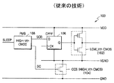
104 MOSスイッチ
106 CPFF
108 PMB
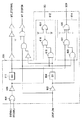
300 MTCOMOS制御回路
302 初期化制御回路
304 タイミング制御回路
EXTWKU,RTCWKU,STOP_ON 内部制御信号
SC 第1制御信号
SCB 第2制御信号
GND 接地電圧
VDD 電源電圧
VGND 仮想接地電圧
Claims (10)
- 論理回路部と、スイッチング部と、フリップフロップ部と、
MTCMOS装置の全体電力を調節する制御回路を含む電力調節部と、を有し、
前記制御回路は、第1制御信号及び第2制御信号を生成し、
前記スイッチング部は、前記第1制御信号に応答する相対的に高いしきい電圧であり、
前記論理回路部は、相対的に低いしきい電圧であり、
前記フリップフロップは、前記第2制御信号に応答して前記低いしきい電圧の論理回路部のデータを保存し、
前記制御回路は、初期化に必要な初期化制御回路と、スリープモードと活性モードの転換時に必要なタイミング制御回路を含み、
前記制御回路は、
MTCMOS装置が活性モードからスリープモードに変更される時、前記第2制御信号の論理状態を第1論理状態から第2論理状態に転換し、所定の遅延時間tD1後、前記第1制御信号の論理状態を前記第2論理状態から前記第1論理状態に転換し、
前記MTCMOS装置が前記スリープモードから前記活性モードに変更される時、前記第1制御信号の論理状態を前記第1論理状態から前記第2論理状態に転換し、前記tD1とは異なる所定の遅延時間tD2後、前記第2制御信号の論理状態を前記第2論理状態から前記第1論理状態に転換させる、ことを特徴とするMTCMOS装置。 - 前記制御回路は、所定のウェークアップ信号EXTWKU,RTCWKUに応答して前記MTCMOS装置をスリープモードから活性モードに転換させ、所定の停止信号STOP_ONに応答して前記MTCMOS装置を前記活性モードから前記スリープモードに転換させることを特徴とする請求項1に記載のMTCMOS装置。
- 前記第1制御信号は、前記第2論理状態である時に前記電流制御スイッチをターンオンさせ、前記第1論理状態である時に前記電流制御スイッチをターンオフさせ、
前記第2制御信号は、前記第2論理状態である時に前記フリップフロップ部を通じて前記論理回路部のデータを保存し、前記第1論理状態である時に前記フリップフロップ部をディセーブルさせることを特徴とする請求項1に記載のMTCMOS装置。 - 前記制御回路は、
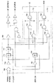
外部の停止信号STOP_ONを入力される第1バッファと、
前記第1バッファから出力された信号を遅延させる第1遅延回路と、
外部の第1ウェークアップ信号EXTWKUと第2ウェークアップ信号RTCWKUとを入力される第1ORゲートと、
前記第1ORゲートから出力された信号を受ける第1インバータと、
前記第1インバータから出力された信号を遅延させる第2遅延回路と、
前記第1インバータの出力信号、前記停止信号STOP_ON及び前記第1遅延回路の出力信号を入力されて1つ以上の論理動作を行って、前記第1制御信号を出力する第1制御信号出力部と、
前記第1バッファの出力信号、前記停止信号及び前記第2遅延回路の出力信号を入力されて1つ以上の論理動作を行って、前記第2制御信号を出力する第2制御信号出力部と、を含むことを特徴とする請求項1に記載のMTCMOS装置。 - 前記第1遅延回路は、1つのフリップフロップを含み、
前記第2遅延回路は、直列に連結された複数のフリップフロップを含むことを特徴とする請求項4に記載のMTCMOS装置。 - 前記第1制御信号出力部は、
前記停止信号及び前記第1遅延回路の出力信号を入力される第1ANDゲートと、
前記第1ANDゲートの出力信号及び前記第1インバータの出力信号を入力される第1NANDゲートと、
前記第1NANDゲートの出力信号及び所定の2つの制御信号を入力されて第1制御信号を出力する第2ORゲートと、を含むことを特徴とする請求項4又は5に記載のMTCMOS装置。 - 前記第2制御信号出力部は、
前記停止信号及び前記第1バッファの出力信号を入力される第2ANDゲートと、
前記第2ANDゲートの出力信号及び前記第2遅延回路の出力信号を入力される第3ANDゲートと、
前記第3ANDゲートの出力信号及び所定の2つの制御信号を入力されて第2制御信号を出力する第4ANDゲートと、を含むことを特徴とする請求項4又は5に記載のMTCMOS装置。 - 第1制御信号に応答する相対的に高いしきい電圧のスイッチング部と、相対的に低い
しきい電圧の論理回路部と、第2制御信号に応答して前記低いしきい電圧の論理回路部の
データを保存するフリップフロップと、MTCMOS装置の全体電力を調節する制御回路を含む電力調節部と、を有し、前記制御回路は、第1制御信号及び第2制御信号を生成し、前記制御回路は、初期化に必要な初期化制御回路と、スリープモードと活性モードの転換時に必要なタイミング制御回路を含むMTCMOS装置の制御方法において、
前記MTCMOS装置のスリープモードへの進入に応答して、前記第2制御信号の論理
状態を転換し、第1遅延後、前記第1制御信号の論理状態を転換する段階と、
前記MTCMOS装置の活性モードへの進入に応答して、前記第1制御信号の論理状態
を転換し、前記第1遅延とは異なる第2遅延後、前記第2制御信号の論理状態を転換する
段階と、を有することを特徴とするMTCMOS装置の制御方法。 - 前記第2遅延は、前記第1遅延より長いことを特徴とする請求項8に記載のMTCMOS装置の制御方法。
- 前記MTCMOS装置のスリープモードへの進入に応答して、前記第2制御信号の論理状態を転換し、第1遅延後、前記第1制御信号の論理状態を転換する段階では、前記MTCMOS装置のスリープモードへの進入に応答して、前記第2制御信号の論理状態を第1論理状態から第2論理状態に転換し、前記第1遅延後、前記第1制御信号の論理状態を前記第2論理状態から前記第1論理状態に転換し、
前記MTCMOS装置の活性モードへの進入に応答して、前記第1制御信号の論理状態を転換し、前記第1遅延とは異なる第2遅延後、前記第2制御信号の論理状態を転換する段階では、前記MTCMOS装置の活性モードへの進入に応答して、前記第1制御信号の論理状態を前記第1論理状態から前記第2論理状態に転換し、前記第1遅延とは異なる前記第2遅延後、前記第2制御信号の論理状態を前記第2論理状態から前記第1論理状態に転換することを特徴とする請求項8に記載のMTCMOS装置の制御方法。
Applications Claiming Priority (2)
| Application Number | Priority Date | Filing Date | Title |
|---|---|---|---|
| KR1020040005598A KR100574967B1 (ko) | 2004-01-29 | 2004-01-29 | Mtcmos용 제어회로 |
| KR2004-005598 | 2004-01-29 |
Publications (3)
| Publication Number | Publication Date |
|---|---|
| JP2005218099A JP2005218099A (ja) | 2005-08-11 |
| JP2005218099A5 JP2005218099A5 (ja) | 2008-02-14 |
| JP5010104B2 true JP5010104B2 (ja) | 2012-08-29 |
Family
ID=34806011
Family Applications (1)
| Application Number | Title | Priority Date | Filing Date |
|---|---|---|---|
| JP2005017129A Active JP5010104B2 (ja) | 2004-01-29 | 2005-01-25 | Mtcmos装置及びその制御方法 |
Country Status (3)
| Country | Link |
|---|---|
| US (1) | US7215155B2 (ja) |
| JP (1) | JP5010104B2 (ja) |
| KR (1) | KR100574967B1 (ja) |
Families Citing this family (23)
| Publication number | Priority date | Publication date | Assignee | Title |
|---|---|---|---|---|
| KR101045295B1 (ko) | 2004-04-29 | 2011-06-29 | 삼성전자주식회사 | Mtcmos 플립-플롭, 그를 포함하는 mtcmos회로, 및 그 생성 방법 |
| KR100564634B1 (ko) * | 2004-10-08 | 2006-03-28 | 삼성전자주식회사 | 단락전류 방지회로를 구비한 mtcmos 회로 시스템 |
| EP1834406A1 (en) * | 2004-11-30 | 2007-09-19 | Freescale Semiconductor Inc. | Apparatus and method for reducing power consumption using selective power gating |
| US20060273391A1 (en) * | 2005-06-01 | 2006-12-07 | Diaz Carlos H | CMOS devices for low power integrated circuits |
| US7391233B1 (en) * | 2007-10-30 | 2008-06-24 | International Business Machines Corporation | Method and apparatus for extending lifetime reliability of digital logic devices through removal of aging mechanisms |
| US7391232B1 (en) * | 2007-10-30 | 2008-06-24 | International Business Machines Corporation | Method and apparatus for extending lifetime reliability of digital logic devices through reversal of aging mechanisms |
| KR101477512B1 (ko) * | 2008-03-18 | 2014-12-31 | 삼성전자주식회사 | 액티브 클럭 쉴딩 구조의 회로 및 이를 포함하는 반도체집적 회로 |
| KR101003153B1 (ko) * | 2009-05-15 | 2010-12-21 | 주식회사 하이닉스반도체 | 전압 안정화 회로 및 이를 이용한 반도체 메모리 장치 |
| US8026741B2 (en) * | 2009-07-31 | 2011-09-27 | Apple Inc. | CMOS circuitry with mixed transistor parameters |
| US7977972B2 (en) * | 2009-08-07 | 2011-07-12 | The Board Of Trustees Of The University Of Arkansas | Ultra-low power multi-threshold asynchronous circuit design |
| US8736332B2 (en) | 2009-12-17 | 2014-05-27 | Lsi Corporation | Leakage current reduction in a sequential circuit |
| US8390331B2 (en) * | 2009-12-29 | 2013-03-05 | Nxp B.V. | Flexible CMOS library architecture for leakage power and variability reduction |
| US8738940B2 (en) | 2011-09-06 | 2014-05-27 | Lsi Corporation | Power controller for SoC power gating applications |
| US8669800B2 (en) * | 2012-02-24 | 2014-03-11 | International Business Machines Corporation | Implementing power saving self powering down latch structure |
| US9094013B2 (en) | 2013-05-24 | 2015-07-28 | The Board Of Trustees Of The University Of Arkansas | Single component sleep-convention logic (SCL) modules |
| US9287858B1 (en) | 2014-09-03 | 2016-03-15 | Texas Instruments Incorporated | Low leakage shadow latch-based multi-threshold CMOS sequential circuit |
| WO2016118183A1 (en) | 2015-01-24 | 2016-07-28 | Schober Susan Marya | Passive phased injection locked circuit |
| CA3031736A1 (en) | 2015-07-29 | 2017-02-02 | Circuit Seed, Llc | Complementary current field-effect transistor devices and amplifiers |
| CN108141181A (zh) * | 2015-07-30 | 2018-06-08 | 电路种子有限责任公司 | 多级式且前馈补偿的互补电流场效应晶体管放大器 |
| WO2017019978A1 (en) | 2015-07-30 | 2017-02-02 | Circuit Seed, Llc | Low noise trans-impedance amplifiers based on complementary current field-effect transistor devices |
| WO2017019981A1 (en) | 2015-07-30 | 2017-02-02 | Circuit Seed, Llc | Reference generator and current source transistor based on complementary current field-effect transistor devices |
| CA3043989A1 (en) | 2015-12-14 | 2017-06-22 | Circuit Seed, Llc | Super-saturation current field effect transistor and trans-impedance mos device |
| KR102420005B1 (ko) * | 2017-12-21 | 2022-07-12 | 에스케이하이닉스 주식회사 | 파워 게이팅 제어 회로 |
Family Cites Families (10)
| Publication number | Priority date | Publication date | Assignee | Title |
|---|---|---|---|---|
| TW334532B (en) | 1996-07-05 | 1998-06-21 | Matsushita Electric Ind Co Ltd | The inspection system of semiconductor IC and the method of generation |
| TW365007B (en) | 1996-12-27 | 1999-07-21 | Matsushita Electric Ind Co Ltd | Driving method of semiconductor integrated circuit and the semiconductor integrated circuit |
| JP3856892B2 (ja) * | 1997-03-03 | 2006-12-13 | 日本電信電話株式会社 | 自己同期型パイプラインデータパス回路および非同期信号制御回路 |
| JPH10261946A (ja) * | 1997-03-19 | 1998-09-29 | Mitsubishi Electric Corp | 半導体集積回路 |
| JPH11112297A (ja) * | 1997-10-06 | 1999-04-23 | Nec Corp | ラッチ回路及びこのラッチ回路を有する半導体集積回路 |
| WO1999066640A1 (en) | 1998-06-18 | 1999-12-23 | Hitachi, Ltd. | Semiconductor integrated circuit |
| JP3878431B2 (ja) * | 2000-06-16 | 2007-02-07 | 株式会社ルネサステクノロジ | 半導体集積回路装置 |
| JP3727838B2 (ja) * | 2000-09-27 | 2005-12-21 | 株式会社東芝 | 半導体集積回路 |
| JP3864248B2 (ja) * | 2001-12-17 | 2006-12-27 | インターナショナル・ビジネス・マシーンズ・コーポレーション | 半導体装置 |
| JP3986393B2 (ja) * | 2002-08-27 | 2007-10-03 | 富士通株式会社 | 不揮発性データ記憶回路を有する集積回路装置 |
-
2004
- 2004-01-29 KR KR1020040005598A patent/KR100574967B1/ko active IP Right Grant
- 2004-11-23 US US10/996,084 patent/US7215155B2/en active Active
-
2005
- 2005-01-25 JP JP2005017129A patent/JP5010104B2/ja active Active
Also Published As
| Publication number | Publication date |
|---|---|
| KR20050077921A (ko) | 2005-08-04 |
| KR100574967B1 (ko) | 2006-04-28 |
| US7215155B2 (en) | 2007-05-08 |
| US20050168242A1 (en) | 2005-08-04 |
| JP2005218099A (ja) | 2005-08-11 |
Similar Documents
| Publication | Publication Date | Title |
|---|---|---|
| JP5010104B2 (ja) | Mtcmos装置及びその制御方法 | |
| US7453300B2 (en) | MTCMOS flip-flop, circuit including the MTCMOS flip-flop, and method of forming the MTCMOS flip-flop | |
| JP2931776B2 (ja) | 半導体集積回路 | |
| US7486108B2 (en) | Charge recycling power gate | |
| US7982514B2 (en) | State-retentive master-slave flip flop to reduce standby leakage current | |
| US6586982B2 (en) | Semiconductor circuit having a combination circuit being switched between an active and inactive state | |
| US8289060B2 (en) | Pulsed state retention power gating flip-flop | |
| JP5285643B2 (ja) | 半導体集積回路および電子情報機器 | |
| US6836175B2 (en) | Semiconductor integrated circuit with sleep memory | |
| US7420403B2 (en) | Latch circuit and flip-flop | |
| JP4220326B2 (ja) | Mtcmos用クロックド・スキャン・フリップフロップ | |
| KR100559738B1 (ko) | 멀티-쓰래쉬홀드 시모스 제어 장치, 멀티-쓰래쉬홀드 시모스 집적 회로 및 멀티-쓰래쉬홀드 시모스 제어 방법 | |
| US7917776B2 (en) | System-on-chip including deepstop mode to reduce total leakage current and method thereof | |
| US6927614B2 (en) | High performance state saving circuit | |
| US20090201063A1 (en) | Dynamic semiconductor device | |
| KR100914553B1 (ko) | 반도체 집적회로 | |
| JP2006222952A (ja) | マルチ−しきいcmosシステム及び複数個のブロックを制御する方法 | |
| KR20040044690A (ko) | 초기화 기능을 갖는 mtcmos 기술을 이용한 cp플립플롭 회로 | |
| WO2003009300A1 (en) | Integrated circuit and battery powered device | |
| JP2004336432A (ja) | 半導体集積回路 |
Legal Events
| Date | Code | Title | Description |
|---|---|---|---|
| A521 | Request for written amendment filed |
Free format text: JAPANESE INTERMEDIATE CODE: A523 Effective date: 20071218 |
|
| A621 | Written request for application examination |
Free format text: JAPANESE INTERMEDIATE CODE: A621 Effective date: 20071218 |
|
| RD02 | Notification of acceptance of power of attorney |
Free format text: JAPANESE INTERMEDIATE CODE: A7422 Effective date: 20080207 |
|
| RD04 | Notification of resignation of power of attorney |
Free format text: JAPANESE INTERMEDIATE CODE: A7424 Effective date: 20080222 |
|
| A977 | Report on retrieval |
Free format text: JAPANESE INTERMEDIATE CODE: A971007 Effective date: 20101221 |
|
| A131 | Notification of reasons for refusal |
Free format text: JAPANESE INTERMEDIATE CODE: A131 Effective date: 20110125 |
|
| A521 | Request for written amendment filed |
Free format text: JAPANESE INTERMEDIATE CODE: A523 Effective date: 20110421 |
|
| A02 | Decision of refusal |
Free format text: JAPANESE INTERMEDIATE CODE: A02 Effective date: 20111122 |
|
| A521 | Request for written amendment filed |
Free format text: JAPANESE INTERMEDIATE CODE: A523 Effective date: 20120322 |
|
| A911 | Transfer to examiner for re-examination before appeal (zenchi) |
Free format text: JAPANESE INTERMEDIATE CODE: A911 Effective date: 20120329 |
|
| TRDD | Decision of grant or rejection written | ||
| A01 | Written decision to grant a patent or to grant a registration (utility model) |
Free format text: JAPANESE INTERMEDIATE CODE: A01 Effective date: 20120508 |
|
| A01 | Written decision to grant a patent or to grant a registration (utility model) |
Free format text: JAPANESE INTERMEDIATE CODE: A01 |
|
| A61 | First payment of annual fees (during grant procedure) |
Free format text: JAPANESE INTERMEDIATE CODE: A61 Effective date: 20120601 |
|
| R150 | Certificate of patent or registration of utility model |
Free format text: JAPANESE INTERMEDIATE CODE: R150 Ref document number: 5010104 Country of ref document: JP Free format text: JAPANESE INTERMEDIATE CODE: R150 |
|
| FPAY | Renewal fee payment (event date is renewal date of database) |
Free format text: PAYMENT UNTIL: 20150608 Year of fee payment: 3 |
|
| R250 | Receipt of annual fees |
Free format text: JAPANESE INTERMEDIATE CODE: R250 |
|
| R250 | Receipt of annual fees |
Free format text: JAPANESE INTERMEDIATE CODE: R250 |
|
| R250 | Receipt of annual fees |
Free format text: JAPANESE INTERMEDIATE CODE: R250 |
|
| R250 | Receipt of annual fees |
Free format text: JAPANESE INTERMEDIATE CODE: R250 |
|
| R250 | Receipt of annual fees |
Free format text: JAPANESE INTERMEDIATE CODE: R250 |
|
| R250 | Receipt of annual fees |
Free format text: JAPANESE INTERMEDIATE CODE: R250 |
|
| R250 | Receipt of annual fees |
Free format text: JAPANESE INTERMEDIATE CODE: R250 |
|
| R250 | Receipt of annual fees |
Free format text: JAPANESE INTERMEDIATE CODE: R250 |
|
| R250 | Receipt of annual fees |
Free format text: JAPANESE INTERMEDIATE CODE: R250 |