JP5010104B2 - MTCMOS device and control method thereof - Google Patents
MTCMOS device and control method thereof Download PDFInfo
- Publication number
- JP5010104B2 JP5010104B2 JP2005017129A JP2005017129A JP5010104B2 JP 5010104 B2 JP5010104 B2 JP 5010104B2 JP 2005017129 A JP2005017129 A JP 2005017129A JP 2005017129 A JP2005017129 A JP 2005017129A JP 5010104 B2 JP5010104 B2 JP 5010104B2
- Authority
- JP
- Japan
- Prior art keywords
- logic state
- control signal
- signal
- control
- mtcmos
- Prior art date
- Legal status (The legal status is an assumption and is not a legal conclusion. Google has not performed a legal analysis and makes no representation as to the accuracy of the status listed.)
- Active
Links
- 238000000034 method Methods 0.000 title claims description 15
- 230000007704 transition Effects 0.000 claims description 19
- 230000004044 response Effects 0.000 claims description 13
- 230000004913 activation Effects 0.000 description 17
- 238000010586 diagram Methods 0.000 description 13
- 238000005516 engineering process Methods 0.000 description 11
- 230000003111 delayed effect Effects 0.000 description 7
- 230000001934 delay Effects 0.000 description 5
- 230000000295 complement effect Effects 0.000 description 4
- 230000008901 benefit Effects 0.000 description 3
- 230000008859 change Effects 0.000 description 3
- 230000008569 process Effects 0.000 description 3
- 239000004065 semiconductor Substances 0.000 description 3
- 238000006243 chemical reaction Methods 0.000 description 1
- 229910044991 metal oxide Inorganic materials 0.000 description 1
- 150000004706 metal oxides Chemical class 0.000 description 1
- 230000004048 modification Effects 0.000 description 1
- 238000012986 modification Methods 0.000 description 1
Images


Classifications
-
- F—MECHANICAL ENGINEERING; LIGHTING; HEATING; WEAPONS; BLASTING
- F16—ENGINEERING ELEMENTS AND UNITS; GENERAL MEASURES FOR PRODUCING AND MAINTAINING EFFECTIVE FUNCTIONING OF MACHINES OR INSTALLATIONS; THERMAL INSULATION IN GENERAL
- F16B—DEVICES FOR FASTENING OR SECURING CONSTRUCTIONAL ELEMENTS OR MACHINE PARTS TOGETHER, e.g. NAILS, BOLTS, CIRCLIPS, CLAMPS, CLIPS OR WEDGES; JOINTS OR JOINTING
- F16B11/00—Connecting constructional elements or machine parts by sticking or pressing them together, e.g. cold pressure welding
- F16B11/006—Connecting constructional elements or machine parts by sticking or pressing them together, e.g. cold pressure welding by gluing
-
- H—ELECTRICITY
- H03—ELECTRONIC CIRCUITRY
- H03K—PULSE TECHNIQUE
- H03K19/00—Logic circuits, i.e. having at least two inputs acting on one output; Inverting circuits
- H03K19/02—Logic circuits, i.e. having at least two inputs acting on one output; Inverting circuits using specified components
- H03K19/08—Logic circuits, i.e. having at least two inputs acting on one output; Inverting circuits using specified components using semiconductor devices
- H03K19/094—Logic circuits, i.e. having at least two inputs acting on one output; Inverting circuits using specified components using semiconductor devices using field-effect transistors
- H03K19/096—Synchronous circuits, i.e. using clock signals
- H03K19/0963—Synchronous circuits, i.e. using clock signals using transistors of complementary type
-
- F—MECHANICAL ENGINEERING; LIGHTING; HEATING; WEAPONS; BLASTING
- F16—ENGINEERING ELEMENTS AND UNITS; GENERAL MEASURES FOR PRODUCING AND MAINTAINING EFFECTIVE FUNCTIONING OF MACHINES OR INSTALLATIONS; THERMAL INSULATION IN GENERAL
- F16B—DEVICES FOR FASTENING OR SECURING CONSTRUCTIONAL ELEMENTS OR MACHINE PARTS TOGETHER, e.g. NAILS, BOLTS, CIRCLIPS, CLAMPS, CLIPS OR WEDGES; JOINTS OR JOINTING
- F16B37/00—Nuts or like thread-engaging members
- F16B37/04—Devices for fastening nuts to surfaces, e.g. sheets, plates
-
- H—ELECTRICITY
- H03—ELECTRONIC CIRCUITRY
- H03K—PULSE TECHNIQUE
- H03K19/00—Logic circuits, i.e. having at least two inputs acting on one output; Inverting circuits
- H03K19/0008—Arrangements for reducing power consumption
- H03K19/0016—Arrangements for reducing power consumption by using a control or a clock signal, e.g. in order to apply power supply
Description
本発明はMTCMOS(Multi−Threshold Complementary Metal Oxide Semiconductor)に係り、具体的には、MTCMOS装置及びその制御方法に関する。 The present invention relates to an MTCMOS (Multi-Threshold Complementary Metal Oxide Semiconductor), and more specifically, to an MTCMOS device and a control method thereof .
MTCMOS技術は、低電力集積回路装置に広く使われる。特に、集積回路装置の電力浪費は、供給される電源電圧を下げることによって減少させうる。しかし、電源電圧の減少は、装置内のトランジスタの速度を低下させる。したがって、このような動作速度の低下を克服するために、トランジスタのしきい電圧(Vth)を下げる。しかし、しきい電圧の減少は、トランジスタが‘オフ’状態である時、トランジスタの漏れ電流または待機電流を増加させて、装置が待機状態である時に電力消耗を増加させてしまう。 MTCMOS technology is widely used in low power integrated circuit devices. In particular, the power consumption of the integrated circuit device can be reduced by lowering the supplied power supply voltage. However, the decrease in power supply voltage reduces the speed of the transistors in the device. Therefore, in order to overcome such a decrease in operating speed, the threshold voltage (Vth) of the transistor is lowered. However, reducing the threshold voltage increases the leakage current or standby current of the transistor when the transistor is in the “off” state, and increases power consumption when the device is in the standby state.
MTCMOS技術は、大きいしきい電圧を有するトランジスタを通じて論理ゲートに電源電圧及び/または接地電圧を供給し、半導体装置の論理動作のためには低いしきい電圧のトランジスタを利用して待機電流の増加問題を克服する。高いしきい電圧を有するトランジスタがターンオンされて論理ゲートに電源電圧を供給する時、低いしきい電圧を有するトランジスタは、低いしきい電圧によって速い速度で動作できる。一方、待機モードである時、高いしきい電圧のトランジスタがターンオフされて電源電圧を低いしきい電圧のトランジスタに供給することを遮断すれば、低いしきい電圧のトランジスタを通じた漏れ電流を減少または除去しうる。 In the MTCMOS technology, a power supply voltage and / or a ground voltage is supplied to a logic gate through a transistor having a large threshold voltage, and a low threshold voltage transistor is used for logic operation of a semiconductor device. Overcome. When a transistor having a high threshold voltage is turned on to supply a power supply voltage to the logic gate, a transistor having a low threshold voltage can operate at a high speed with a low threshold voltage. On the other hand, when in standby mode, if the high threshold voltage transistor is turned off to prevent the supply voltage from being supplied to the low threshold voltage transistor, the leakage current through the low threshold voltage transistor is reduced or eliminated. Yes.
MTCMOS装置は、供給電源と論理回路との間にしきい電圧が相対的に高いMOSスイッチを直列に連結した構造を有する。 The MTCMOS device has a structure in which MOS switches having a relatively high threshold voltage are connected in series between a power supply and a logic circuit.
前記MTCMOS技術は、活性モードでは、前記MOSスイッチをオンさせて前記供給電源を前記論理回路に供給し、スリープモードでは、前記MOSスイッチをオフさせて前記供給電源を前記論理回路から遮断してシステム全体の電力を最小化できる。 In the MTCMOS technology, in the active mode, the MOS switch is turned on to supply the power supply to the logic circuit, and in the sleep mode, the MOS switch is turned off to shut off the supply power from the logic circuit. The overall power can be minimized.
特に、この技術は、活性モードよりスリープモードに該当する時間が長いシステムに使われる回路の消費電力の減少に非常に有用である。しかし、供給電源が遮断された時に対応した特別な手段を講じなければ、MTCMOS回路は、スリープモード時に仮想グラウンド電圧レベルがフローティング状態になるため、これに連結したラッチ回路やフリップフロップの保存データが損失される短所がある。したがって、MTCMOSを正常的に動作させるためには、スリープモード時にデータを保存できる所定のフリップフロップ回路とそれを制御するための制御回路とが必要である。 In particular, this technique is very useful for reducing the power consumption of a circuit used in a system in which the time corresponding to the sleep mode is longer than the active mode. However, unless special measures are taken when the power supply is cut off, the MTCMOS circuit has a virtual ground voltage level in a floating state in the sleep mode. There are disadvantages to be lost. Therefore, in order to operate the MTCMOS normally, a predetermined flip-flop circuit capable of storing data in the sleep mode and a control circuit for controlling it are necessary.
本発明が解決しようとする技術的課題は、MTCMOSの動作中、スリープモードに進入する時と活性モードに復帰する時、データを保存するフリップフロップ部及び電流スイッチの動作を制御する制御信号の出力を制御するためのMTCMOS制御回路を有するMTCMOS装置及びその制御方法を提供することである。 The technical problem to be solved by the present invention is to output a control signal for controlling the operation of the flip-flop unit for storing data and the current switch when entering the sleep mode and returning to the active mode during the operation of the MTCMOS. It is an object to provide an MTCMOS device having an MTCMOS control circuit for controlling the above and a control method thereof.
前記目的を達成するためになされた本発明によるMTCMOS装置は、論理回路部と、スイッチング部と、フリップフロップ部と、MTCMOS装置の全体電力を調節する制御回路を含む電力調節部と、を有し、第1制御信号及び第2制御信号を生成する制御回路と、前記第1制御信号に応答する相対的に高いしきい電圧の前記スイッチング部と、相対的に低いしきい電圧の論理回路部と、前記低いしきい電圧の論理回路部のデータを保存し、前記第2制御信号に応答するフリップフロップと、を有し、前記制御回路は、初期化に必要な初期化制御回路と、スリープモードと活性モードの転換時に必要なタイミング制御回路を含み、前記制御回路は、前記MTCMOS装置が活性モードからスリープモードに変更される時、前記第2制御信号の論理状態を第1論理状態から第2論理状態に転換し、所定遅延時間tD1後、前記第1制御信号の論理状態を前記第2論理状態から前記第1論理状態に転換し、前記MTCMOS装置が前記スリープモードから前記活性モードに変更する時、前記第1制御信号の論理状態を前記第1論理状態から前記第2論理状態に転換し、前記tD1とは異なる所定遅延時間tD2後、前記第2制御信号の論理状態を前記第2論理状態から前記第1論理状態に転換させることを特徴とする。
An MTCMOS device according to the present invention made to achieve the above object includes a logic circuit unit, a switching unit, a flip-flop unit, and a power adjustment unit including a control circuit for adjusting the overall power of the MTCMOS device. a control circuit for generating a first control signal and the second control signal, and the switching portion of the relatively high threshold voltage responsive to said first control signal, and a logic circuit portion of the relatively low threshold voltage A flip-flop that stores data of the logic circuit unit having the low threshold voltage and responds to the second control signal, the control circuit including an initialization control circuit required for initialization, and a sleep mode. and includes timing control circuitry required for conversion of active mode, the control circuit, when the MTCMOS device is changed from the active mode to the sleep mode, the second control signal The logic state is changed from the first logic state to the second logic state, and after a predetermined delay time tD1, the logic state of the first control signal is changed from the second logic state to the first logic state. When changing from the sleep mode to the active mode, the logic state of the first control signal is changed from the first logic state to the second logic state, and after the predetermined delay time tD2 different from the tD1, The logic state of the control signal is changed from the second logic state to the first logic state.
MTCMOSを制御するMTCMOS制御回路は、前記MTCMOSのスリープモードによって高電圧の電流制御スイッチのスイッチングを制御する第1制御信号SCと、論理回路部のデータを保存するためのフリップフロップ部を制御する第2制御信号SCBとを出力し、前記MTCMOSがスリープモードに転換される時は、前記MTCMOS制御回路は、前記第2制御信号を第1論理状態から第2論理状態に遷移し、所定の遅延時間tD1後に前記第1制御信号を第2論理状態から第1論理状態に遷移し、前記MTCMOSが活性モードに転換される時は、前記MTCMOS制御回路は、前記第1制御信号を第1論理状態から第2論理状態に遷移し、所定の遅延時間tD2後に前記第2制御信号を第2論理状態から第1論理状態に遷移する。 The MTCMOS control circuit for controlling the MTCMOS controls a first control signal SC for controlling switching of a high voltage current control switch according to the sleep mode of the MTCMOS and a flip-flop unit for storing data of the logic circuit unit. When the MTCMOS is switched to the sleep mode, the MTCMOS control circuit changes the second control signal from the first logic state to the second logic state and outputs a predetermined delay time. When the first control signal changes from the second logic state to the first logic state after tD1, and the MTCMOS is switched to the active mode, the MTCMOS control circuit changes the first control signal from the first logic state. Transition to the second logic state, and after a predetermined delay time tD2, transition the second control signal from the second logic state to the first logic state That.
望ましくは、前記MTCMOS制御回路は、所定のウェークアップ信号EXTWKU,RTCWKUに応答して前記MTCMOSを活性モードに転換させ、所定の停止信号STOP_ONに応答して前記MTCMOSをスリープモードに転換させる。 Preferably, the MTCMOS control circuit switches the MTCMOS to an active mode in response to predetermined wakeup signals EXTWKU and RTCWKU, and switches the MTCMOS to a sleep mode in response to a predetermined stop signal STOP_ON.
さらに望ましくは、前記第1制御信号は、前記第2論理状態である時に前記電流制御スイッチをターンオンさせ、前記第1論理状態である時に前記電流制御スイッチをターンオフさせ、前記第2制御信号は、前記第2論理状態である時に前記フリップフロップ部を通じて前記論理回路部のデータを保存し、前記第1論理状態である時に前記フリップフロップ部をディセーブルさせる。 More preferably, the first control signal turns on the current control switch when in the second logic state, turns off the current control switch when in the first logic state, and the second control signal is The data of the logic circuit unit is stored through the flip-flop unit when in the second logic state, and the flip-flop unit is disabled when in the first logic state.
本発明の一実施例によるMTCMOS制御回路は、外部の停止信号STOP_ONを入力される第1バッファ、前記第1バッファから出力された信号を遅延させる第1遅延回路、外部の第1ウェークアップ信号EXTWKUと第2ウェークアップ信号RTCWKUとを入力される第1ORゲート、前記第1ORゲートから出力された信号を受ける第1インバータ、前記第1インバータから出力された信号を遅延させる第2遅延回路、前記第1インバータの出力信号、前記停止信号及び前記第1遅延回路の出力信号を入力されて前記第1制御信号SCを出力する第1制御信号出力部、及び前記第1バッファの出力信号、前記停止信号及び前記第2遅延回路の出力信号を入力されて前記第2制御信号SCBを出力する第2制御信号出力部を含む。 An MTCMOS control circuit according to an embodiment of the present invention includes a first buffer to which an external stop signal STOP_ON is input, a first delay circuit for delaying a signal output from the first buffer, an external first wake-up signal EXTWKU, A first OR gate that receives a second wake-up signal RTCWKU; a first inverter that receives a signal output from the first OR gate; a second delay circuit that delays a signal output from the first inverter; and the first inverter The first control signal output unit that receives the output signal, the stop signal, and the output signal of the first delay circuit and outputs the first control signal SC, and the output signal of the first buffer, the stop signal, and the A second control signal output unit that receives the output signal of the second delay circuit and outputs the second control signal SCB;
本発明の他の実施例によるMTCMOS制御回路は、前記第1遅延回路は、1つのフリップフロップより構成され、前記第2遅延回路は、2つの直列に連結されたフリップフロップより構成される。 In the MTCMOS control circuit according to another embodiment of the present invention, the first delay circuit is composed of one flip-flop, and the second delay circuit is composed of two flip-flops connected in series.
望ましくは、前記第1制御信号出力部は、前記停止信号及び前記第1遅延回路の出力信号を入力される第1ANDゲート、前記第1ANDゲートの出力信号及び前記第1インバータの出力信号を入力される第1NANDゲート、及び前記第1NANDゲートの出力信号及び所定の2つの制御信号を入力されて第1制御信号を出力する第2ORゲートを含む。 Preferably, the first control signal output unit receives a first AND gate to which the stop signal and the output signal of the first delay circuit are input, an output signal of the first AND gate, and an output signal of the first inverter. And a second OR gate that receives the output signal of the first NAND gate and two predetermined control signals and outputs the first control signal.
望ましくは、前記第2制御信号出力部は、前記停止信号及び前記第1バッファの出力信号を入力される第2ANDゲート、前記第2ANDゲートの出力信号及び前記第2遅延回路の出力信号を入力される第3ANDゲート、及び前記第3ANDゲートの出力信号及び所定の2つの制御信号を入力されて第2制御信号を出力する第4ANDゲートを含む。 Preferably, the second control signal output unit receives a second AND gate to which the stop signal and the output signal of the first buffer are input, an output signal of the second AND gate, and an output signal of the second delay circuit. And a fourth AND gate that receives the output signal of the third AND gate and two predetermined control signals and outputs the second control signal.
本発明のさらに他の実施例によるMTCMOSを制御するMTCMOS制御回路は、前記MTCMOSのスリープモードによって高電圧の電流制御スイッチのスイッチングを制御する第1制御信号SCと、論理回路部のデータを保存するためのフリップフロップ部を制御する第2制御信号SCBとを出力し、前記MTCMOSがスリープモードに転換される時は、前記MTCMOS制御回路は、前記第2制御信号を第1論理状態から第2論理状態に遷移し、所定の遅延時間tD1後に、前記第1制御信号を第2論理状態から第1論理状態に遷移し、前記MTCMOSが活性モードに転換される時は、前記MTCMOS制御回路は、前記第1制御信号を第1論理状態から第2論理状態に遷移し、所定の遅延時間tD2後に、前記第2制御信号を第2論理状態から第1論理状態に遷移するタイミング制御回路と、前記MTCMOSの初期化で内部のリセットフリップフロップを初期化し、前記リセットフリップフロップから出力される信号を通じて前記第1制御信号を第2論理状態に初期化し、前記第2制御信号を第1論理状態に初期化する初期化制御回路とを含む。 The MTCMOS control circuit for controlling the MTCMOS according to another embodiment of the present invention stores the first control signal SC for controlling the switching of the high voltage current control switch according to the MTCMOS sleep mode and the data of the logic circuit unit. When the MTCMOS is switched to the sleep mode, the MTCMOS control circuit changes the second control signal from the first logic state to the second logic. Transition to a state, and after a predetermined delay time tD1, the first control signal transitions from a second logic state to a first logic state, and when the MTCMOS is switched to an active mode, the MTCMOS control circuit The first control signal transitions from the first logic state to the second logic state, and after the predetermined delay time tD2, the second control signal is A timing control circuit that transitions from a two logic state to a first logic state, and an internal reset flip-flop is initialized by initialization of the MTCMOS, and the first control signal is transmitted to the second logic through a signal output from the reset flip-flop. And an initialization control circuit that initializes the second control signal to a first logic state.
本発明によるMTCMOSの活性モードを制御する方法は、所定の幅を有するロジックハイパルスを有する所定のウェークアップ信号EXTWKU,RTCWKUを出力する段階、前記所定のウェークアップ信号に応答して前記MTCMOSの電流の流れを制御する第1制御信号をロジックハイに遷移する段階、前記第1制御信号がロジックハイに遷移した後、所定の遅延時間後に、前記MTCMOSの論理回路部のデータを保存するためのフリップフロップ部を制御する第2制御信号をロジックローに遷移する段階、及び前記MTCMOSをスリープモードに転換させる停止信号STOP_ONをロジックローに遷移する段階を含む。 The method for controlling the active mode of the MTCMOS according to the present invention includes the steps of outputting predetermined wakeup signals EXTWKU and RTCWKU having logic high pulses having a predetermined width, and current flow of the MTCMOS in response to the predetermined wakeup signal. A flip-flop unit for storing data of the logic circuit unit of the MTCMOS after transitioning the first control signal for controlling the logic to logic high, a predetermined delay time after the first control signal transitions to logic high Transition of the second control signal for controlling the signal to logic low, and transition of the stop signal STOP_ON for switching the MTCMOS to the sleep mode to logic low.
本発明によるMTCMOSのスリープモードを制御する方法は、前記MTCMOSをスリープモードに転換させる停止信号STOP_ONをロジックハイに遷移する段階、前記停止信号に応答して前記MTCMOSの論理回路部のデータを保存するためのフリップフロップ部を制御する第2制御信号をロジックハイに遷移する段階、及び前記第2制御信号がロジックハイに遷移した後、所定の遅延時間後に、前記MTCMOSの電流の流れを制御する第1制御信号をロジックローに遷移する段階を含む。 The method for controlling the sleep mode of the MTCMOS according to the present invention includes a step of transitioning the stop signal STOP_ON for switching the MTCMOS to the sleep mode to logic high, and storing data of the logic circuit unit of the MTCMOS in response to the stop signal. And a second control signal for controlling the flip-flop unit for controlling the current flow of the MTCMOS after a predetermined delay time after the second control signal transitions to a logic high, and after the second control signal transitions to a logic high. Transitioning one control signal to a logic low.
本発明によるMTCMOSによれば、MTCMOS内部制御信号をMTCMOSの各モード転換時、適切な遅延時間を通じて制御することによって、MTCMOSのスリープモードに転換時にデータを正常的に保存でき、活性化モード時に充電された電荷を完全に放電して、MTCMOSの動作中にデータを損傷せずに消費電力を最小化しつつも正常的な動作を制御可能にする。 According to the MTCMOS according to the present invention, the MTCMOS internal control signal is controlled through an appropriate delay time when switching each mode of the MTCMOS, so that data can be normally stored when switching to the sleep mode of the MTCMOS and charged during the activation mode. The discharged charge is completely discharged, so that normal operation can be controlled while minimizing power consumption without damaging data during operation of the MTCMOS.
本発明と本発明の動作の利点及び本発明の実施によって達成される目的を十分に理解するためには、本発明の望ましい実施例を例示する添付図面及び図面に記載された内容を参照しなければならない。 For a full understanding of the invention and the advantages of the invention and the objectives achieved by the practice of the invention, reference should be made to the accompanying drawings and the description thereof that illustrate preferred embodiments of the invention. I must.
以下、添付された図面を参照して本発明の望ましい実施例を説明することによって、本発明を詳細に説明する。各図面に提示された同じ参照符号は同じ部材を表す。 Hereinafter, exemplary embodiments of the present invention will be described in detail with reference to the accompanying drawings. The same reference numerals provided in each drawing represent the same member.
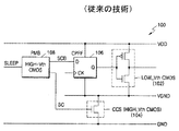
図1は、一般的なMTCMOSの構造を示すブロック図である。 FIG. 1 is a block diagram showing the structure of a general MTCMOS.
図1を参照すれば、MTCMOS装置100は、電源電圧の第1電源電圧VDDと仮想接地電圧である第1動作電圧VGNDとの間に論理回路部102(ここでは、“低いしきい電圧を有する論理回路部”または簡単に“論理回路部”と呼ばれる)を有し、仮想接地電圧VGNDと接地電圧である第2電源電圧GNDとの間にMTCMOS 100の動作如何をスイッチングするスイッチング部104(ここでは、“高いしきい電圧を有する回路制御スイッチ”と呼ばれる)を備える。また、論理回路部102のデータを保存できるフリップフロップ部106(ここでは、簡単に“フリップフロップ”と呼ばれる)及びMTCMOSの全体電力を調節する電力調節部(Power Management Block:PMB)108を備える。
Referring to FIG. 1, the
MTCMOSは、1V以下の低電力電源領域で、電源電圧または接地電圧と論理回路部102との間にしきい電圧Vthが比較的高いMOSスイッチ104を直列に連結して回路を動作させる場合、すなわち活性化モードである場合に、このMOSスイッチ104をターンオンさせて電源電圧VDDまたは接地電圧GNDをしきい電圧Vthが比較的低い論理回路部102に供給して論理回路部102の動作速度を向上させ、論理回路部102の回路を使用していない場合、すなわちスリープモードには、MOSスイッチ104をターンオフさせて論理回路部102に電源電圧VDDまたは接地電圧GNDを遮断して、論理回路部102の漏れ電流を減らして、全体的なシステムの消費電力を最小化できる。
MTCMOS is an active circuit in which a
また、MTCMOSは、MOSスイッチ104による面積の増大は生じるが、全体的な工程上の大きい変化なしにも設計の流れの修正のみで直ちに具現が可能であるという長所もある。
In addition, the MTCMOS has an advantage that the area can be increased by the
MTCMOS100は、活性化モード時間よりスリープモード時間が長い携帯用LSIの消費電力を減らすのに非常に有用である。しかし、MOSスイッチ104がターンオフされる場合、論理回路部102に保存されているデータが損失されてしまう問題がある。
The MTCMOS 100 is very useful for reducing the power consumption of a portable LSI whose sleep mode time is longer than the activation mode time. However, when the
これを解決するための技術であって、{S.Mutoh,et al.,1V High−Speed Digital Circuit Technology with 0.5mm Multithreshold−Voltage CMOS,IEEE Int.ASIC Conf.,Sept.,pp.186〜189.1993}及び[S.Mutoh,et al.,A1−V Power Supply High−Speed Digital Circuit Technology with Multithreshold−Voltage CMOS,IEEE JSSC,Vol.30.No.8,pp.847〜853,1995]に記述されたConventional MTCMOS FF技術と、
[S.Shigematsu,et al.,A1−V high−speed MTCMOS circuit scheme for power−down applications,VLSI Symp.,pp.125〜126,1995]、[S.Mutoh,et al.,A1−V Multithreshold−Voltage CMOS Digital Signal Processor for Mobile Phone Application,IEEE JSSC,Vol.31.No.11,pp.1795〜1802,1996]及び[S.Shigematsu,et al.,A1−V High−Speed MTCMOS Circuit Scheme for Power−Down Application Circuit,IEEE JSSC,Vol.32.No.6,pp.861〜869,1997]に開示されたBalloon FF技術と、
[H.Makino,et al.,An Auto−Backgate−Controlled MT−CMOS Circuit,VLSI Symp.,pp.42〜43,1998]に記述されたABC(Auto Backgate Controlled)−MTCMOS技術と、[K.Kumagai,et al.,A Novel Powering−down Scheme for Low Vt CMOS Circuit,VLSI Symp.,pp.44〜45,1998]に記述されたVRC(Virtual power/ground Rail Clamp)技術と、
[K.T.Park,H.S.Won,et al,“A New Low−Power Edge−Triggered and Logic−Embeded FF Using Complementary Pass−Transistors Circuit”,ITC−CSCC,2001]に記述されたCPFF(Complementary Pass−transistor Flip Flop)技術と、がある。
A technique for solving this problem is described in {S. Mutoh, et al., 1V High-Speed Digital Circuit Technology with 0.5 mm Multithreshold-Voltage CMOS, IEEE Int. ASIC Conf., Sept., pp. 186-189.1993} and [S. Mutoh, et al., A1-V Power Supply High-Speed Digital Circuit Technology Vs. No. 8, pp. 847-853, 1995], a conventional MTCMOS FF technology;
[S. Shigematsu, et al., A1-V high-speed MTCMOS circuit scheme for power-down applications, VLSI Symp., Pp. 125-126, 1995], [S. Mutoh, et al. -Voltage CMOS Digital Signal Processor for Mobile Phone Application, IEEE JSSC, Vol. No. 11, pp. 1795 to 1802, 1996] and [S. Shigematsu, et al., A1-V High-Speed MTCMOS Circuit Scheme for Power-Down Application Circuit, IEEE JSSC, Vol. 32. No. 6, pp. 861-869, 1997], Ballon FF technology,
ABC (Auto Baccate Controlled) -MTCMOS technology described in [H. Makino, et al., An Auto-Background-Controlled MT-CMOS Circuit, VLSI Symp., Pp. 42-43, 1998], and [K. Kumagai, et al., A Novel Powering-down Schema for Low Vt CMOS Circuit, VLSI Symp., Pp. 44-45, 1998], VRC (Virtual power / ground Rail) technology.
[K.T. Park, H.S. Won, et al, "A New Low-Power Edge-Triggered and Logic-Embedded FF Using Complementary Circuits, FF written in ITC-CSCC, 200, written by ITC-CSCC." Complementary Pass-transistor Flip Flop) technology.
このような解決技術のうちCPFFは、面積、速度、消費電力の側面で優秀な特徴を示す。 Among such solution technologies, CPFF exhibits excellent characteristics in terms of area, speed, and power consumption.
図2は、図1のCPFF 106のCPFF(Complementary Pass transistor−based Flip Flop)についての一実施例を示す回路である。
FIG. 2 is a circuit diagram showing an embodiment of the CPFF (Complementary Pass Transistor-based Flip Flop) of the
Balloon FFのような場合、スリープモードと活性化モード時、フリップフロップを制御するために複雑な制御回路が必要であり、論理回路部のフリップフロップ種類によって制御方式及び回路が異なって設計されなければならないが、図2に示されたCPFFは、狭い面積で低電力、高速動作が可能であり、電源を遮断して回路を動作させないシステムの構成要素として使われる時、ラッチされたデータを保存するための回路をさらに設置する必要がないCPFFである。 In the case of Ballon FF, a complicated control circuit is required to control the flip-flops in the sleep mode and the activation mode, and the control method and circuit must be designed differently depending on the flip-flop type of the logic circuit unit. Although not shown, the CPFF shown in FIG. 2 is capable of low power and high speed operation in a small area and preserves latched data when used as a system component that shuts off the power supply and does not operate the circuit. This is a CPFF that does not require any additional circuit.
図2に示されたCPFFは、クロック信号CLKと前記クロック信号CLKを所定の時間遅延させた遅延クロック信号との間の遅延時間を感知し、前記遅延された時間差に該当する時間の間に入力データを受信し、新たな入力データが受信されるまで以前入力データをラッチする。図2のCPFFは、データを保存するためのタイミング設計が従来のフリップフロップに比べて非常に簡単であるという長所がある。 The CPFF shown in FIG. 2 senses a delay time between a clock signal CLK and a delayed clock signal obtained by delaying the clock signal CLK by a predetermined time, and is input during a time corresponding to the delayed time difference. Data is received and previous input data is latched until new input data is received. The CPFF of FIG. 2 has an advantage that the timing design for storing data is much simpler than the conventional flip-flop.
図1のPMB(Power Management Block)108は、MTCMOS 100のMOSスイッチ(あるいはCCSセル)104を制御するための第1制御信号SCとCPFF 106を制御するための第2制御信号SCBとを出力する。
A PMB (Power Management Block) 108 in FIG. 1 outputs a first control signal SC for controlling the MOS switch (or CCS cell) 104 of the
図1のMTCMOS 100をエラーなしに正常に動作させるためには、PMB 108内にMTCMOS 100の初期化過程とスリープモード及び活性化モードの転換過程とを適切に制御するための制御回路、すなわちMTCMOS制御回路が含まれなければならない。
In order for the
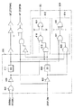
図3は、本発明によるMTCMOS制御回路を示すブロック図である。 FIG. 3 is a block diagram showing an MTCMOS control circuit according to the present invention.
図3を参照すれば、MTCMOS制御回路300は、MTCMOSの初期化に必要な初期化制御回路302及びスリープモードと活性化モードの転換時に必要なタイミング制御回路304を含む。また、MTCMOS制御回路300は、図1のPMB 108の内部制御信号EXTWKU,RTCWKU,STOP_ONを入力され、前記初期化制御回路302及びタイミング制御回路304から出力される信号とPMB内部の他の信号との論理和を通じて第1制御信号SCを出力し、論理積を通じて第2制御信号SCBを出力する。論理部102は、図3で一つのインバータとして示されたが、さらに複雑な形態の論理部がMTCMOS装置内に提供されうる。
Referring to FIG. 3, the
図4は、MTCMOSの初期化に必要な初期化制御回路の回路図である。 FIG. 4 is a circuit diagram of an initialization control circuit necessary for initialization of MTCMOS.
図4に示された初期化制御回路400は、MTCMOSの初期化を制御する部分であって、MTCMOSチップの初期パワーアップ時にPOR(Power−On−Reset)信号を使用してリセットフリップフロップ402をリセットさせて、第1制御信号SCをハイレベルに初期化し、第2制御信号SCBをローレベルに初期化する役割を行う。
The
図4を参照すれば、初期化制御回路400は、リセットフリップフロップ402、ANDゲート404、ORゲート406及びパワーオンリセット回路(NPORST)408より構成されている。リセットフリップフロップ402の入力端RNは、パワーオンリセット回路408の出力端PORと連結されており、リセットフリップフロップ402の出力端Q及びQNは、それぞれ3入力ANDゲート404、3入力ORゲート406に連結され、AND回路の出力は第2制御信号SCBであり、ORゲートの出力は第1制御信号SCである。
Referring to FIG. 4, the
MTCMOS回路の初期化時、3入力ANDゲート404及び3入力ORゲート406の異なる入力信号は、ローレベルまたはハイレベルに固定されている。
When the MTCMOS circuit is initialized, different input signals of the 3-input AND
リセットフリップフロップ402の入力信号は、パワーオンリセット回路408の出力信号であって、電源電圧VDDが適正電圧以上になった場合、出力信号が第1論理状態(以下、例えばローレベル)から第2論理状態(以下、たとえばハイレベル)に変更され、この信号は、前記リセットフリップフロップ402回路を初期化させる。
The input signal of the reset flip-
リセットフリップフロップ402の第1出力信号Qは、第1論理状態になり、第2出力信号QNは、第2論理状態になって出力される。これにより、3入力AND回路404の入力信号としてリセットフリップフロップ402の第1出力信号Qが印加されることによって、AND回路404の出力信号である第2制御信号SCBは、第1論理状態を維持し、これはMTCMOSの特定フリップフロップCPFFの入力信号に連結される。
The first output signal Q of the reset flip-
一方、OR回路406の入力信号としてリセットフリップフロップ402の第2出力信号QNが印加されることによって、OR回路406の出力の第1制御信号SCは、第2論理状態を維持する。また、MTCMOS回路の初期化時、AND回路404の他の入力信号は、第2論理状態に固定されており、OR回路406の他の入力信号は、第1論理状態に固定されている。
On the other hand, when the second output signal QN of the reset flip-
一方、MTCMOS制御回路に必要な他の1つは、MTCMOSチップの動作のうちスリープモードに進入する時と活性化モードに進入する時、第1及び第2制御信号のタイミングを制御するタイミング制御回路304である。 Meanwhile, another one necessary for the MTCMOS control circuit is a timing control circuit for controlling the timing of the first and second control signals when entering the sleep mode and entering the activation mode among the operations of the MTCMOS chip. 304.
本発明によるタイミング制御回路304は、MTCMOSがスリープモードに入る時、あらかじめCPFFにデータを保存できるように第1制御信号と第2制御信号との間に適切な遅延時間をおいてタイミング関係を調節し、また、MTCMOSが活性化モードに入る時にも、CPFFに保存されたデータをMTCMOSの論理回路部で適切に利用できるように前記第1制御信号と前記第2制御信号との間に適切な遅延時間をおくように制御する役割を行う。
The
図5は、本発明によるタイミング制御回路の入出力信号を示すタイミング図である。 FIG. 5 is a timing diagram showing input / output signals of the timing control circuit according to the present invention.
図5を参照すれば、図5は、図3のMTCMOS制御回路に入力される入力信号EXTWKU,RTCWKU,STOP_ONと出力される制御信号SC,SCBとのタイミング関係を示している。 Referring to FIG. 5, FIG. 5 shows a timing relationship between the input signals EXTWKU, RTCWKU, and STOP_ON input to the MTCMOS control circuit of FIG. 3 and the output control signals SC and SCB.
まず、MTCMOSが活性化モードで、スリープモードに転換される場合を説明すれば、外部の2つのウェークアップ信号EXTWKU,RTCWKUは、第1論理状態に留まっており、MTCMOSをスリープモードに進入するように指示する所定の停止信号STOP_ONは、第1論理状態から第2論理状態に遷移する。それにより、第2論理状態に遷移された停止信号STOP_ONを入力されたタイミング制御回路304は、CPFFを制御する第2制御信号SCBを第1論理状態から第2論理状態に遷移させて出力する。そして、第1遅延時間tD1後にタイミング制御回路304は、MOSスイッチング部CCSを制御する第1制御信号SCを第2論理状態から第1論理状態に遷移させて出力する。
First, the case where the MTCMOS is switched to the sleep mode in the activation mode will be described. The two external wake-up signals EXTWKU and RTCWKU remain in the first logic state so that the MTCMOS enters the sleep mode. The predetermined stop signal STOP_ON to be instructed transits from the first logic state to the second logic state. As a result, the
それにより、第2制御信号SCBが第2論理状態になると、MTCMOSの論理回路部のラッチやフリップフロップに保存されたデータをCPFFに保存する。次いで、第1遅延時間tD1後に第1制御信号SCが第1論理状態になると、MOSスイッチ部CCSがターンオフされ、MTCMOSは、スリープモードに遷移される。 As a result, when the second control signal SCB enters the second logic state, the data stored in the latch or flip-flop of the MTCMOS logic circuit is stored in the CPFF. Next, when the first control signal SC becomes the first logic state after the first delay time tD1, the MOS switch unit CCS is turned off, and the MTCMOS transitions to the sleep mode.
したがって、MTCMOSがスリープモードに遷移される前に論理回路部のデータをCPFFに保存する。 Therefore, the data of the logic circuit section is stored in the CPFF before the MTCMOS transitions to the sleep mode.
MTCMOSがスリープモードから活性化モードに転換される場合を説明すれば、MTCMOSを活性化モードに転換させるために、外部の2つのウェークアップ信号EXTWKU,RTCWKUが第1論理状態から第2論理状態を有するパルス信号に転換されてMTCMOS制御回路に入力される。それにより、タイミング制御回路304は、MOSスイッチング部CCSを制御する第1制御信号CSを第1論理状態からMOSスイッチング部をターンオンさせる第2制御状態に遷移させて出力する。そして、第2遅延時間tD2後にタイミング制御回路304は、CPFFを制御する第2制御信号SCBを第2論理状態からCPFFをディセーブルする第1論理状態に遷移させて出力する。次いで、所定の停止信号STOP_ONは、第2論理状態から第1論理状態に遷移される。
If the MTCMOS is switched from the sleep mode to the activation mode, the two external wake-up signals EXTWKU and RTCWKU have the second logic state from the first logic state in order to switch the MTCMOS to the activation mode. It is converted into a pulse signal and input to the MTCMOS control circuit. As a result, the
ここで、第2遅延時間tD2は、スリープモードから活性化モードに転換される時、スリープモード時、チャージされた第1動作電源、すなわち仮想接地電源VGNDの電荷を完全放電するまでにかかる時間であって、全体の仮想接地電源VGNDネットワークのRC時定数によって決定される。 Here, the second delay time tD2 is a time taken to completely discharge the charge of the charged first operation power supply, that is, the virtual ground power supply VGND in the sleep mode when switching from the sleep mode to the activation mode. And determined by the RC time constant of the entire virtual ground power supply VGND network.
それにより、第1制御信号SCが第2論理状態になってMOSスイッチングに入力されれば、MTCMOSのMOSスイッチング部は、ターンオンして論理回路部に電流を供給す。したがって、MTCMOSは、活性化モードになって論理回路部が動作される。また、この状態で、第2制御信号SCBは第2論理状態であるため、CPFFにはデータがそのまま保存されており、論理回路部は、CPFFに保存されたデータを利用してスリープモードに転換される前のデータを回復できる。次いで、第2遅延時間tD2後に第2制御信号SCBが第2論理状態から第1論理状態に遷移されて、CPFFはディセーブル状態になる。 Accordingly, when the first control signal SC enters the second logic state and is input to the MOS switching, the MOS switching unit of the MTCMOS is turned on to supply current to the logic circuit unit. Therefore, MTCMOS is in the activation mode and the logic circuit section is operated. In this state, since the second control signal SCB is in the second logic state, the data is stored in the CPFF as it is, and the logic circuit unit switches to the sleep mode using the data stored in the CPFF. You can recover the data before it is done. Next, after the second delay time tD2, the second control signal SCB transitions from the second logic state to the first logic state, and the CPFF is disabled.
したがって、MTCMOSが活性化モードに遷移された後にもCPFFに保存されたデータを読出して利用できる。 Therefore, data stored in the CPFF can be read and used even after the MTCMOS transitions to the activation mode.
図6は、図5の動作のための本発明の一実施例によるタイミング制御回路の回路図である。 FIG. 6 is a circuit diagram of a timing control circuit according to an embodiment of the present invention for the operation of FIG.
図6を参照すれば、タイミング制御回路600は、外部の停止信号STOP_ONを受ける第1バッファ602、前記第1バッファ602から出力された信号を遅延させる第1遅延回路604、外部の第1ウェークアップ信号EXTWKUと第2ウェークアップ信号RTCWKUとを入力される第1ORゲート606、前記第1ORゲート606から出力された信号を受ける第1インバータ608、前記第1インバータ608から出力された信号を遅延させる第2遅延回路610、前記第1インバータ608、前記停止信号STOP_ON及び前記第1遅延回路604の出力信号を入力されて前記第1制御信号SCを出力する第1制御信号出力部612及び前記第1バッファ602、前記停止信号STOP_ON及び前記第2遅延回路610の出力信号を入力されて前記第2制御信号SCBを出力する第2制御信号出力部614を含む。
Referring to FIG. 6, a
また、前記第1制御信号出力部612は、前記停止信号STOP_ON及び前記第1遅延回路604の出力信号を入力される第1ANDゲート616、前記第1ANDゲート616の出力信号及び前記第1インバータ608の出力信号を入力される第1NANDゲート618及び前記第1NANDゲート618の出力信号及び所定の2つの制御信号‘0’を入力されて第1制御信号SCを出力する第2ORゲート620を含む。
The first control
この時、3入力ORゲート620の異なる2つの入力信号は、第1論理状態に固定されている。
At this time, two different input signals of the three-input OR
また、前記第2制御信号出力部614は、前記停止信号STOP_ON及び前記第1バッファ602の出力信号を入力される第2ANDゲート622、前記第2ANDゲート622の出力信号及び前記第2遅延回路610の出力信号を入力される第3ANDゲート624及び前記第3ANDゲート624の出力信号及び所定の2つの制御信号‘1’を入力されて第2制御信号SCBを出力する第4ANDゲート626を含む。
In addition, the second control
この時、3入力ANDゲート626の異なる2つの入力信号は、第2論理状態に固定されている。
At this time, two different input signals of the 3-input AND
図6に示されたタイミング制御回路は、MTCMOSが活性化モードからスリープモードに転換する時、外部ウェークアップ信号EXTWKU,RTCWKUは、常に第1論理状態を維持し、停止信号STOP_ONが第1論理状態から第2論理状態に転換する時、第2制御信号SCBが第1論理状態から第2論理状態に転移される。また、第1遅延回路604によって第1遅延時間tD1ほど遅延されて第1制御信号SCが第2論理状態から第1論理状態に転移される。
In the timing control circuit shown in FIG. 6, when the MTCMOS switches from the activation mode to the sleep mode, the external wakeup signals EXTTWKU and RTCWKU always maintain the first logic state, and the stop signal STOP_ON changes from the first logic state. When transitioning to the second logic state, the second control signal SCB is transitioned from the first logic state to the second logic state. Also, the first control circuit SC is shifted from the second logic state to the first logic state after being delayed by the
また、MTCMOSがスリープモードから活性化モードに転換される時には、停止信号STOP_ONは、常に第2論理状態を維持し、2つのウェークアップ信号EXTWKU,RTCWKUが第1論理状態から第2論理状態に転換する時、まず第1制御信号SCが第1論理状態から第2論理状態に転移され、第2遅延回路610によって第2遅延時間tD2ほど遅延されて第2制御信号SCBが第2論理状態から第1論理状態に転移される。この時、第2遅延時間tD2は、スリープモード時にチャージされた仮想接地電圧VGNDラインの電荷を完全放電するまでにかかる時間であって、全体の仮想接地ネックワークのRC時定数を考慮して決定される。
Further, when the MTCMOS is switched from the sleep mode to the activation mode, the stop signal STOP_ON always maintains the second logic state, and the two wake-up signals EXTWKU and RTCWKU change from the first logic state to the second logic state. First, the first control signal SC is changed from the first logic state to the second logic state, and is delayed by the second delay time tD2 by the
図7は、図5の動作のための本発明の他の実施例によるタイミング制御回路の回路図である。 FIG. 7 is a circuit diagram of a timing control circuit according to another embodiment of the present invention for the operation of FIG.
図7を参照すれば、タイミング制御回路700は、外部の停止信号STOP_ONを受ける第1バッファ702、前記第1バッファ702から出力された信号を遅延させる第1フリップフロップ704、外部の第1ウェークアップ信号EXTWKUと第2ウェークアップ信号RTCWKUとを入力される第1ORゲート706、前記第1ORゲート706から出力された信号を受ける第1インバータ708、前記第1インバータ708から出力された信号を遅延させる直列に連結された第2フリップフロップ710と第3フリップフロップ711、前記第1インバータ708、前記停止信号STOP_ON及び前記第1フリップフロップ704の出力信号を入力されて前記第1制御信号SCを出力する第1制御信号出力部712及び前記第1バッファ702、前記停止信号STOP_ON及び前記第3フリップフロップ711の出力信号を入力されて前記第2制御信号SCBを出力する第2制御信号出力部714を含む。
Referring to FIG. 7, a
また、前記第1制御信号出力部712は、前記停止信号STOP_ON及び前記第1フリップフロップ704の出力信号を入力される第1ANDゲート716、前記第1ANDゲート716の出力信号及び前記第1インバータ708の出力信号を入力される第1NANDゲート718及び前記第1NANDゲート718の出力信号及び所定の2つの制御信号‘0’を入力されて第1制御信号SCを出力する第2 ORゲート720を含む。
In addition, the first control
この時、3入力ORゲート720の異なる2つの入力信号は、第1論理状態に固定されている。
At this time, two different input signals of the three-input OR
また、前記第2制御信号出力部714は、前記停止信号STOP_ON及び前記第1バッファ702の出力信号を入力される第2ANDゲート722、前記第2ANDゲート722の出力信号及び前記第3フリップフロップ711の出力信号を入力される第3ANDゲート724及び前記第3ANDゲート724の出力信号及び所定の2つの制御信号‘1’を入力されて第2制御信号SCBを出力する第4ANDゲート726を含む。
In addition, the second control
この時、3入力ANDゲート726の異なる2つの入力信号は、第2論理状態に固定されている。
At this time, two different input signals of the 3-input AND
また、図7のフリップフロップを通じた遅延時間は、クロック信号RTC_CLKの周期ほど遅延されて決定される。 Further, the delay time through the flip-flop of FIG. 7 is determined by being delayed by the period of the clock signal RTC_CLK.
図7に示されたタイミング制御回路は、MTCMOSが活性化モードからスリープモードに転換する時、外部ウェークアップ信号EXTWKU,RTCWKUは常に第1論理状態を維持し、停止信号STOP_ONが第1論理状態から第2論理状態に転換する時、第2制御信号SCBが第1論理状態から第2論理状態に転移される。また、第1フリップフロップ704によって第1遅延時間tD1ほど遅延されて第1制御信号SCが第2論理状態から第1論理状態に転移される。
In the timing control circuit shown in FIG. 7, when the MTCMOS switches from the activation mode to the sleep mode, the external wake-up signals EXTWKU and RTCWKU always maintain the first logic state, and the stop signal STOP_ON changes from the first logic state to the first logic state. When switching to the two logic state, the second control signal SCB is transitioned from the first logic state to the second logic state. In addition, the first control signal SC is shifted from the second logic state to the first logic state after being delayed by the first flip-
また、MTCMOSがスリープモードから活性化モードに転換される時には、停止信号STOP_ONは常に第2論理状態を維持し、2つのウェークアップ信号EXTWKU,RTCWKUが第1論理状態から第2論理状態に転換する時、まず第1制御信号SCが第1論理状態から第2論理状態に転移され、第2フリップフロップ710と第3フロップ711から成る第2遅延回路によって第2遅延時間tD2ほど遅延されて第2制御信号SCBが第2論理状態から第1論理状態に転移される。この時、第2遅延時間tD2は、スリープモード時にチャージされた仮想接地電圧VGNDラインの電荷を完全放電するまでにかかる時間であって、全体の仮想接地ネックワークのRC時定数を考慮して決定される。
When the MTCMOS is switched from the sleep mode to the activation mode, the stop signal STOP_ON always maintains the second logic state, and when the two wake-up signals EXTWKU and RTCWKU change from the first logic state to the second logic state. First, the first control signal SC is shifted from the first logic state to the second logic state, and is delayed by the second delay time tD2 by the second delay circuit composed of the second flip-
本発明は、図面に示された一実施例を参考として説明されたが、これは例示的なものに過ぎず、当業者ならば、これから多様な変形及び均等な他の実施例が可能であることが分かる。したがって、本発明の真の技術的保護範囲は、特許請求の範囲の技術的思想によって決定されなければならない。 Although the present invention has been described with reference to one embodiment shown in the drawings, this is by way of example only, and various modifications and equivalent other embodiments can be made by those skilled in the art. I understand that. Therefore, the true technical protection scope of the present invention must be determined by the technical idea of the claims.
本発明によるMTCMOSによれば、低電力を利用した集積回路に利用され、多様なLSIまたはメモリ半導体装置に使用されうる。 The MTCMOS according to the present invention is used in an integrated circuit using low power and can be used in various LSI or memory semiconductor devices.
102 論理部
104 MOSスイッチ
106 CPFF
108 PMB
300 MTCOMOS制御回路
302 初期化制御回路
304 タイミング制御回路
EXTWKU,RTCWKU,STOP_ON 内部制御信号
SC 第1制御信号
SCB 第2制御信号
GND 接地電圧
VDD 電源電圧
VGND 仮想接地電圧
102
108 PMB
300
Claims (10)
MTCMOS装置の全体電力を調節する制御回路を含む電力調節部と、を有し、
前記制御回路は、第1制御信号及び第2制御信号を生成し、
前記スイッチング部は、前記第1制御信号に応答する相対的に高いしきい電圧であり、
前記論理回路部は、相対的に低いしきい電圧であり、
前記フリップフロップは、前記第2制御信号に応答して前記低いしきい電圧の論理回路部のデータを保存し、
前記制御回路は、初期化に必要な初期化制御回路と、スリープモードと活性モードの転換時に必要なタイミング制御回路を含み、
前記制御回路は、
MTCMOS装置が活性モードからスリープモードに変更される時、前記第2制御信号の論理状態を第1論理状態から第2論理状態に転換し、所定の遅延時間tD1後、前記第1制御信号の論理状態を前記第2論理状態から前記第1論理状態に転換し、
前記MTCMOS装置が前記スリープモードから前記活性モードに変更される時、前記第1制御信号の論理状態を前記第1論理状態から前記第2論理状態に転換し、前記tD1とは異なる所定の遅延時間tD2後、前記第2制御信号の論理状態を前記第2論理状態から前記第1論理状態に転換させる、ことを特徴とするMTCMOS装置。 A logic circuit section, a switching section, a flip-flop section,
A power adjustment unit including a control circuit for adjusting the overall power of the MTCMOS device,
The control circuit generates a first control signal and a second control signal,
The switching unit is a relatively high threshold voltage responsive to the first control signal;
The logic circuit portion has a relatively low threshold voltage;
The flip-flop stores data of the logic circuit unit having the low threshold voltage in response to the second control signal;
The control circuit includes an initialization control circuit necessary for initialization, and a timing control circuit necessary for switching between the sleep mode and the active mode,
The control circuit includes:
When the MTCMOS device is changed from the active mode to the sleep mode, the logic state of the second control signal is changed from the first logic state to the second logic state, and after a predetermined delay time tD1, the logic of the first control signal is changed. Changing the state from the second logic state to the first logic state;
When the MTCMOS device is changed from the sleep mode to the active mode, the logic state of the first control signal is changed from the first logic state to the second logic state, and a predetermined delay time different from the tD1 After tD2, the MTCMOS device changes the logic state of the second control signal from the second logic state to the first logic state.
前記第2制御信号は、前記第2論理状態である時に前記フリップフロップ部を通じて前記論理回路部のデータを保存し、前記第1論理状態である時に前記フリップフロップ部をディセーブルさせることを特徴とする請求項1に記載のMTCMOS装置。 The first control signal turns on the current control switch when in the second logic state and turns off the current control switch when in the first logic state;
The second control signal stores data of the logic circuit unit through the flip-flop unit when in the second logic state, and disables the flip-flop unit when in the first logic state. The MTCMOS device according to claim 1.
外部の停止信号STOP_ONを入力される第1バッファと、
前記第1バッファから出力された信号を遅延させる第1遅延回路と、
外部の第1ウェークアップ信号EXTWKUと第2ウェークアップ信号RTCWKUとを入力される第1ORゲートと、
前記第1ORゲートから出力された信号を受ける第1インバータと、
前記第1インバータから出力された信号を遅延させる第2遅延回路と、
前記第1インバータの出力信号、前記停止信号STOP_ON及び前記第1遅延回路の出力信号を入力されて1つ以上の論理動作を行って、前記第1制御信号を出力する第1制御信号出力部と、
前記第1バッファの出力信号、前記停止信号及び前記第2遅延回路の出力信号を入力されて1つ以上の論理動作を行って、前記第2制御信号を出力する第2制御信号出力部と、を含むことを特徴とする請求項1に記載のMTCMOS装置。 The control circuit includes:
A first buffer to which an external stop signal STOP_ON is input;
A first delay circuit for delaying a signal output from the first buffer;
A first OR gate to which an external first wakeup signal EXTWKU and a second wakeup signal RTCWKU are input;
A first inverter for receiving a signal output from the first OR gate;
A second delay circuit for delaying the signal output from the first inverter;
A first control signal output unit configured to receive at least one logic operation by receiving the output signal of the first inverter, the stop signal STOP_ON, and the output signal of the first delay circuit, and to output the first control signal; ,
A second control signal output unit that receives the output signal of the first buffer, the stop signal, and the output signal of the second delay circuit, performs one or more logical operations, and outputs the second control signal; The MTCMOS device of claim 1, comprising:
前記第2遅延回路は、直列に連結された複数のフリップフロップを含むことを特徴とする請求項4に記載のMTCMOS装置。 The first delay circuit includes one flip-flop,
5. The MTCMOS device of claim 4, wherein the second delay circuit includes a plurality of flip-flops connected in series.
前記停止信号及び前記第1遅延回路の出力信号を入力される第1ANDゲートと、
前記第1ANDゲートの出力信号及び前記第1インバータの出力信号を入力される第1NANDゲートと、
前記第1NANDゲートの出力信号及び所定の2つの制御信号を入力されて第1制御信号を出力する第2ORゲートと、を含むことを特徴とする請求項4又は5に記載のMTCMOS装置。 The first control signal output unit includes:
A first AND gate that receives the stop signal and the output signal of the first delay circuit;
A first NAND gate that receives an output signal of the first AND gate and an output signal of the first inverter;
6. The MTCMOS device according to claim 4, further comprising: a second OR gate that receives the output signal of the first NAND gate and two predetermined control signals and outputs the first control signal.
前記停止信号及び前記第1バッファの出力信号を入力される第2ANDゲートと、
前記第2ANDゲートの出力信号及び前記第2遅延回路の出力信号を入力される第3ANDゲートと、
前記第3ANDゲートの出力信号及び所定の2つの制御信号を入力されて第2制御信号を出力する第4ANDゲートと、を含むことを特徴とする請求項4又は5に記載のMTCMOS装置。 The second control signal output unit includes:
A second AND gate that receives the stop signal and the output signal of the first buffer;
A third AND gate that receives the output signal of the second AND gate and the output signal of the second delay circuit;
6. The MTCMOS device according to claim 4, further comprising: a fourth AND gate that receives the output signal of the third AND gate and two predetermined control signals and outputs the second control signal.
しきい電圧の論理回路部と、第2制御信号に応答して前記低いしきい電圧の論理回路部の
データを保存するフリップフロップと、MTCMOS装置の全体電力を調節する制御回路を含む電力調節部と、を有し、前記制御回路は、第1制御信号及び第2制御信号を生成し、前記制御回路は、初期化に必要な初期化制御回路と、スリープモードと活性モードの転換時に必要なタイミング制御回路を含むMTCMOS装置の制御方法において、
前記MTCMOS装置のスリープモードへの進入に応答して、前記第2制御信号の論理
状態を転換し、第1遅延後、前記第1制御信号の論理状態を転換する段階と、
前記MTCMOS装置の活性モードへの進入に応答して、前記第1制御信号の論理状態
を転換し、前記第1遅延とは異なる第2遅延後、前記第2制御信号の論理状態を転換する
段階と、を有することを特徴とするMTCMOS装置の制御方法。 A relatively high threshold voltage switching unit responsive to the first control signal, a relatively low threshold voltage logic circuit unit, and a low threshold voltage logic circuit unit responsive to the second control signal . A flip-flop for storing data and a power adjustment unit including a control circuit for adjusting the overall power of the MTCMOS device, wherein the control circuit generates a first control signal and a second control signal. In the control method of the MTCMOS device, the control circuit includes an initialization control circuit necessary for initialization, and a timing control circuit necessary for switching between the sleep mode and the active mode .
Changing the logic state of the second control signal in response to entering the sleep mode of the MTCMOS device, and changing the logic state of the first control signal after a first delay;
In response to the MTCMOS device entering the active mode, changing a logic state of the first control signal and changing a logic state of the second control signal after a second delay different from the first delay. And a method for controlling an MTCMOS device .
前記MTCMOS装置の活性モードへの進入に応答して、前記第1制御信号の論理状態を転換し、前記第1遅延とは異なる第2遅延後、前記第2制御信号の論理状態を転換する段階では、前記MTCMOS装置の活性モードへの進入に応答して、前記第1制御信号の論理状態を前記第1論理状態から前記第2論理状態に転換し、前記第1遅延とは異なる前記第2遅延後、前記第2制御信号の論理状態を前記第2論理状態から前記第1論理状態に転換することを特徴とする請求項8に記載のMTCMOS装置の制御方法。 In response to the MTCMOS device entering a sleep mode, the logic state of the second control signal is changed, and after the first delay, the logic state of the first control signal is changed. In response to entering the mode, the logic state of the second control signal is changed from the first logic state to the second logic state, and after the first delay, the logic state of the first control signal is changed to the second logic state. Transition from state to the first logic state;
In response to the MTCMOS device entering the active mode, changing a logic state of the first control signal and changing a logic state of the second control signal after a second delay different from the first delay. Then, in response to the MTCMOS device entering the active mode, the logic state of the first control signal is changed from the first logic state to the second logic state, which is different from the first delay. after a delay, control method of the MTCMOS device according to claim 8, the logic state of the second control signal, characterized in that switches from said second logic state to said first logic state.
Applications Claiming Priority (2)
| Application Number | Priority Date | Filing Date | Title |
|---|---|---|---|
| KR1020040005598A KR100574967B1 (en) | 2004-01-29 | 2004-01-29 | Controller for Multi-Threshold CMOS |
| KR2004-005598 | 2004-01-29 |
Publications (3)
| Publication Number | Publication Date |
|---|---|
| JP2005218099A JP2005218099A (en) | 2005-08-11 |
| JP2005218099A5 JP2005218099A5 (en) | 2008-02-14 |
| JP5010104B2 true JP5010104B2 (en) | 2012-08-29 |
Family
ID=34806011
Family Applications (1)
| Application Number | Title | Priority Date | Filing Date |
|---|---|---|---|
| JP2005017129A Active JP5010104B2 (en) | 2004-01-29 | 2005-01-25 | MTCMOS device and control method thereof |
Country Status (3)
| Country | Link |
|---|---|
| US (1) | US7215155B2 (en) |
| JP (1) | JP5010104B2 (en) |
| KR (1) | KR100574967B1 (en) |
Families Citing this family (23)
| Publication number | Priority date | Publication date | Assignee | Title |
|---|---|---|---|---|
| KR101045295B1 (en) | 2004-04-29 | 2011-06-29 | 삼성전자주식회사 | MTCMOS flip-flop, MTCMOS circuit including the same, and method for generating the same |
| KR100564634B1 (en) * | 2004-10-08 | 2006-03-28 | 삼성전자주식회사 | Multi-threshold cmos system having a short-circuit current protection circuit |
| US8018247B2 (en) * | 2004-11-30 | 2011-09-13 | Freescale Semiconductor, Inc. | Apparatus and method for reducing power consumption using selective power gating |
| US20060273391A1 (en) * | 2005-06-01 | 2006-12-07 | Diaz Carlos H | CMOS devices for low power integrated circuits |
| US7391233B1 (en) * | 2007-10-30 | 2008-06-24 | International Business Machines Corporation | Method and apparatus for extending lifetime reliability of digital logic devices through removal of aging mechanisms |
| US7391232B1 (en) * | 2007-10-30 | 2008-06-24 | International Business Machines Corporation | Method and apparatus for extending lifetime reliability of digital logic devices through reversal of aging mechanisms |
| KR101477512B1 (en) * | 2008-03-18 | 2014-12-31 | 삼성전자주식회사 | Circuit having an active clock shielding structure, and semiconductor integreated circuit including the same |
| KR101003153B1 (en) * | 2009-05-15 | 2010-12-21 | 주식회사 하이닉스반도체 | Voltage Stabilization Circuit and a Semiconductor Memory Apparatus using the same |
| US8026741B2 (en) * | 2009-07-31 | 2011-09-27 | Apple Inc. | CMOS circuitry with mixed transistor parameters |
| US7977972B2 (en) * | 2009-08-07 | 2011-07-12 | The Board Of Trustees Of The University Of Arkansas | Ultra-low power multi-threshold asynchronous circuit design |
| US8736332B2 (en) * | 2009-12-17 | 2014-05-27 | Lsi Corporation | Leakage current reduction in a sequential circuit |
| US8390331B2 (en) * | 2009-12-29 | 2013-03-05 | Nxp B.V. | Flexible CMOS library architecture for leakage power and variability reduction |
| US8738940B2 (en) | 2011-09-06 | 2014-05-27 | Lsi Corporation | Power controller for SoC power gating applications |
| US8669800B2 (en) * | 2012-02-24 | 2014-03-11 | International Business Machines Corporation | Implementing power saving self powering down latch structure |
| US9094013B2 (en) | 2013-05-24 | 2015-07-28 | The Board Of Trustees Of The University Of Arkansas | Single component sleep-convention logic (SCL) modules |
| US9287858B1 (en) | 2014-09-03 | 2016-03-15 | Texas Instruments Incorporated | Low leakage shadow latch-based multi-threshold CMOS sequential circuit |
| US10367514B2 (en) | 2015-01-24 | 2019-07-30 | Circuit Seed, Llc | Passive phased injection locked circuit |
| US10211781B2 (en) | 2015-07-29 | 2019-02-19 | Circuit Seed, Llc | Complementary current field-effect transistor devices and amplifiers |
| CN108141181A (en) * | 2015-07-30 | 2018-06-08 | 电路种子有限责任公司 | The complementary current FET amplifier of multi-stag and feedforward compensation |
| US10476457B2 (en) | 2015-07-30 | 2019-11-12 | Circuit Seed, Llc | Low noise trans-impedance amplifiers based on complementary current field-effect transistor devices |
| US10514716B2 (en) | 2015-07-30 | 2019-12-24 | Circuit Seed, Llc | Reference generator and current source transistor based on complementary current field-effect transistor devices |
| WO2017105554A1 (en) | 2015-12-14 | 2017-06-22 | Circuit Seed, Llc | Super-saturation current field effect transistor and trans-impedance mos device |
| KR102420005B1 (en) * | 2017-12-21 | 2022-07-12 | 에스케이하이닉스 주식회사 | Power gating control circuit |
Family Cites Families (10)
| Publication number | Priority date | Publication date | Assignee | Title |
|---|---|---|---|---|
| TW334532B (en) | 1996-07-05 | 1998-06-21 | Matsushita Electric Ind Co Ltd | The inspection system of semiconductor IC and the method of generation |
| TW365007B (en) | 1996-12-27 | 1999-07-21 | Matsushita Electric Ind Co Ltd | Driving method of semiconductor integrated circuit and the semiconductor integrated circuit |
| JP3856892B2 (en) * | 1997-03-03 | 2006-12-13 | 日本電信電話株式会社 | Self-synchronous pipeline data path circuit and asynchronous signal control circuit |
| JPH10261946A (en) * | 1997-03-19 | 1998-09-29 | Mitsubishi Electric Corp | Semiconductor integrated circuit |
| JPH11112297A (en) * | 1997-10-06 | 1999-04-23 | Nec Corp | Latch circuit and semiconductor integrated circuit having the same |
| US6433584B1 (en) | 1998-06-18 | 2002-08-13 | Hitachi, Ltd. | Semiconductor integrated circuit |
| JP3878431B2 (en) * | 2000-06-16 | 2007-02-07 | 株式会社ルネサステクノロジ | Semiconductor integrated circuit device |
| JP3727838B2 (en) * | 2000-09-27 | 2005-12-21 | 株式会社東芝 | Semiconductor integrated circuit |
| JP3864248B2 (en) * | 2001-12-17 | 2006-12-27 | インターナショナル・ビジネス・マシーンズ・コーポレーション | Semiconductor device |
| JP3986393B2 (en) * | 2002-08-27 | 2007-10-03 | 富士通株式会社 | Integrated circuit device having nonvolatile data storage circuit |
-
2004
- 2004-01-29 KR KR1020040005598A patent/KR100574967B1/en active IP Right Grant
- 2004-11-23 US US10/996,084 patent/US7215155B2/en active Active
-
2005
- 2005-01-25 JP JP2005017129A patent/JP5010104B2/en active Active
Also Published As
| Publication number | Publication date |
|---|---|
| US20050168242A1 (en) | 2005-08-04 |
| US7215155B2 (en) | 2007-05-08 |
| JP2005218099A (en) | 2005-08-11 |
| KR20050077921A (en) | 2005-08-04 |
| KR100574967B1 (en) | 2006-04-28 |
Similar Documents
| Publication | Publication Date | Title |
|---|---|---|
| JP5010104B2 (en) | MTCMOS device and control method thereof | |
| US7453300B2 (en) | MTCMOS flip-flop, circuit including the MTCMOS flip-flop, and method of forming the MTCMOS flip-flop | |
| JP2931776B2 (en) | Semiconductor integrated circuit | |
| US7486108B2 (en) | Charge recycling power gate | |
| US7982514B2 (en) | State-retentive master-slave flip flop to reduce standby leakage current | |
| US6586982B2 (en) | Semiconductor circuit having a combination circuit being switched between an active and inactive state | |
| US8289060B2 (en) | Pulsed state retention power gating flip-flop | |
| JP5285643B2 (en) | Semiconductor integrated circuit and electronic information equipment | |
| US6836175B2 (en) | Semiconductor integrated circuit with sleep memory | |
| US7420403B2 (en) | Latch circuit and flip-flop | |
| JP4220326B2 (en) | Clocked scan flip-flop for MTCMOS | |
| KR100559738B1 (en) | Multi-threshold cmos control apparatus, multi-threshold cmos integrated circuit and multi-threshold cmos control method | |
| US7917776B2 (en) | System-on-chip including deepstop mode to reduce total leakage current and method thereof | |
| US6927614B2 (en) | High performance state saving circuit | |
| US20090201063A1 (en) | Dynamic semiconductor device | |
| KR100914553B1 (en) | Semiconductor integrated circuit | |
| JP2006222952A (en) | Multi-threshold cmos system, and method for controlling respective blocks | |
| KR20040044690A (en) | Complementary pass transistor flip-flop circuit using mtcmos technology having initialization function | |
| WO2003009300A1 (en) | Integrated circuit and battery powered device | |
| JP2004336432A (en) | Semiconductor integrated circuit |
Legal Events
| Date | Code | Title | Description |
|---|---|---|---|
| A521 | Request for written amendment filed |
Free format text: JAPANESE INTERMEDIATE CODE: A523 Effective date: 20071218 |
|
| A621 | Written request for application examination |
Free format text: JAPANESE INTERMEDIATE CODE: A621 Effective date: 20071218 |
|
| RD02 | Notification of acceptance of power of attorney |
Free format text: JAPANESE INTERMEDIATE CODE: A7422 Effective date: 20080207 |
|
| RD04 | Notification of resignation of power of attorney |
Free format text: JAPANESE INTERMEDIATE CODE: A7424 Effective date: 20080222 |
|
| A977 | Report on retrieval |
Free format text: JAPANESE INTERMEDIATE CODE: A971007 Effective date: 20101221 |
|
| A131 | Notification of reasons for refusal |
Free format text: JAPANESE INTERMEDIATE CODE: A131 Effective date: 20110125 |
|
| A521 | Request for written amendment filed |
Free format text: JAPANESE INTERMEDIATE CODE: A523 Effective date: 20110421 |
|
| A02 | Decision of refusal |
Free format text: JAPANESE INTERMEDIATE CODE: A02 Effective date: 20111122 |
|
| A521 | Request for written amendment filed |
Free format text: JAPANESE INTERMEDIATE CODE: A523 Effective date: 20120322 |
|
| A911 | Transfer to examiner for re-examination before appeal (zenchi) |
Free format text: JAPANESE INTERMEDIATE CODE: A911 Effective date: 20120329 |
|
| TRDD | Decision of grant or rejection written | ||
| A01 | Written decision to grant a patent or to grant a registration (utility model) |
Free format text: JAPANESE INTERMEDIATE CODE: A01 Effective date: 20120508 |
|
| A01 | Written decision to grant a patent or to grant a registration (utility model) |
Free format text: JAPANESE INTERMEDIATE CODE: A01 |
|
| A61 | First payment of annual fees (during grant procedure) |
Free format text: JAPANESE INTERMEDIATE CODE: A61 Effective date: 20120601 |
|
| R150 | Certificate of patent or registration of utility model |
Free format text: JAPANESE INTERMEDIATE CODE: R150 Ref document number: 5010104 Country of ref document: JP Free format text: JAPANESE INTERMEDIATE CODE: R150 |
|
| FPAY | Renewal fee payment (event date is renewal date of database) |
Free format text: PAYMENT UNTIL: 20150608 Year of fee payment: 3 |
|
| R250 | Receipt of annual fees |
Free format text: JAPANESE INTERMEDIATE CODE: R250 |
|
| R250 | Receipt of annual fees |
Free format text: JAPANESE INTERMEDIATE CODE: R250 |
|
| R250 | Receipt of annual fees |
Free format text: JAPANESE INTERMEDIATE CODE: R250 |
|
| R250 | Receipt of annual fees |
Free format text: JAPANESE INTERMEDIATE CODE: R250 |
|
| R250 | Receipt of annual fees |
Free format text: JAPANESE INTERMEDIATE CODE: R250 |
|
| R250 | Receipt of annual fees |
Free format text: JAPANESE INTERMEDIATE CODE: R250 |
|
| R250 | Receipt of annual fees |
Free format text: JAPANESE INTERMEDIATE CODE: R250 |
|
| R250 | Receipt of annual fees |
Free format text: JAPANESE INTERMEDIATE CODE: R250 |
|
| R250 | Receipt of annual fees |
Free format text: JAPANESE INTERMEDIATE CODE: R250 |