JP4996838B2 - Multilayer wiring board - Google Patents
Multilayer wiring board Download PDFInfo
- Publication number
- JP4996838B2 JP4996838B2 JP2005285482A JP2005285482A JP4996838B2 JP 4996838 B2 JP4996838 B2 JP 4996838B2 JP 2005285482 A JP2005285482 A JP 2005285482A JP 2005285482 A JP2005285482 A JP 2005285482A JP 4996838 B2 JP4996838 B2 JP 4996838B2
- Authority
- JP
- Japan
- Prior art keywords
- wiring board
- particles
- multilayer wiring
- conductive paste
- thermoplastic resin
- Prior art date
- Legal status (The legal status is an assumption and is not a legal conclusion. Google has not performed a legal analysis and makes no representation as to the accuracy of the status listed.)
- Expired - Fee Related
Links
Images


Landscapes
- Production Of Multi-Layered Print Wiring Board (AREA)
Description
本発明は、多層配線基板に関し、特に、導電ペースト組成物が充填されたビアホールが形成された配線基板を複数積層してなる多層配線基板に関する。 The present invention relates to a multilayer wiring board, and more particularly to a multilayer wiring board formed by laminating a plurality of wiring boards formed with via holes filled with a conductive paste composition.
高度情報化社会の進展により、電子機器の情報処理の高速化(動作周波数の高速化)、情報通信の周波数広帯域化(ブロードバンド)が進み、電子機器に搭載される基板としては、高密度な多層配線基板が求められている。また、その配線基板材料は、比誘電率、誘電正接が低いことが求められている。 Advances in the highly information-oriented society have led to faster information processing in electronic devices (higher operating frequency) and wider frequency bands for information communications (broadband). There is a need for a wiring board. Further, the wiring board material is required to have a low relative dielectric constant and dielectric loss tangent.
この高密度な多層配線基板としては、90年代より、ガラスエポキシ基板からなるコア基板の上下に感光性エポキシ樹脂からなるビルドアップ層を逐次積み上げたビルドアップ多層基板が提案されている。このビルドアップ多層基板は、従来の多層基板に比較して微細配線が容易なため、今日では、多くの電子機器に採用されている。 As this high-density multilayer wiring board, a buildup multilayer board in which buildup layers made of a photosensitive epoxy resin are successively stacked on and under a core board made of a glass epoxy board has been proposed since the 1990s. This build-up multilayer board is used in many electronic devices today because fine wiring is easier compared to conventional multilayer boards.
しかしながら、ビルドアップ多層配線基板においては、基板の絶縁信頼性を確保する必要上、コア基板の貫通スルーホール径や配線間隔がコア層の上下に積層されるビルドアップ層のビア径や配線間隔に比較して大きい点、また、各層間の接続をするビア配線が銅めっきで形成されているため、製造プロセス上、ビアの上にビアを形成することができない点、といった問題があった。よって、ビルドアップ多層配線基板においては、近年要求されている更なる高密度化に対応するには限界が見えはじめていた。 However, in the build-up multilayer wiring board, it is necessary to ensure the insulation reliability of the board. In comparison, there is a problem that the via wiring for connecting the layers is formed by copper plating, so that the via cannot be formed on the via in the manufacturing process. Therefore, in the build-up multilayer wiring board, the limit has begun to appear in order to cope with the further higher density demanded in recent years.
これらの問題を解決するものとして、最近では、配線設計の自由度が高く、かつ、伝送特性に優れたコアレス全層IVH(Interstitial Via Hole)基板が注目されている。このコアレス全層IVH基板における各層間の接続をするビア配線は導電性ペースト組成物で形成されている。よって、ビアの上にビアを形成するビアオンビア構造、および、パッドオンビア構造を形成することが可能であり、近年の更なる高密度化の要求に十分対応するものである。 As a solution to these problems, a coreless all-layer IVH (Intermediate Via Hole) substrate that has a high degree of freedom in wiring design and excellent transmission characteristics has recently attracted attention. Via wiring for connecting each layer in the coreless all-layer IVH substrate is formed of a conductive paste composition. Therefore, it is possible to form a via-on-via structure and a pad-on-via structure in which a via is formed on the via, and sufficiently meet the recent demand for higher density.
ここで、多層配線基板の高性能化(高密度化、高信頼性化)における最大のポイントは、前述の配線構造にプラスして、各層の厚み方向に形成された導電性ペースト組成物からなるビア配線と、各層の表面に形成された銅箔からなる導体パターンとの接続信頼性を、多層化された際において、十分に確保する点にある。 Here, the greatest point in improving the performance (high density, high reliability) of the multilayer wiring board is made of a conductive paste composition formed in the thickness direction of each layer in addition to the above-described wiring structure. The connection reliability between the via wiring and the conductor pattern made of the copper foil formed on the surface of each layer is sufficiently ensured when multilayered.
多層配線基板に関する従来の技術としては、特許文献1には、従来のビルドアップ多層配線基板の欠点を解消したものとして、配線設計の自由度が高く、スタックドビア構造の実現が可能であり、しかも高速信号伝送に適した全層IVH構造の多層配線基板が提案されている。特許文献1に記載されているところによると、アラミド不織布に熱硬化性樹脂であるエポキシ樹脂を含浸させたシート基板材を用い、このシート基板材に貫通穴を形成する。この貫通穴に、金属粒子とエポキシ等のバインダー樹脂と溶剤からなる導電性ペーストを充填後、乾燥固化する。そして、この基板材の両面に銅箔を熱プレスすることにより、導電性ペーストを硬化させた両面銅張板を作製する。この両面銅張板をエッチングして、両面回路基板を形成する。その後、この両面回路基板の両側に、前記シート基板材(プリプレグ)を配置し、さらにそれらの外側に銅箔を配置して、熱プレスすることにより、4層のインナビアホール構造を持つ多層配線基板が形成される。
As a conventional technique related to a multilayer wiring board,
非特許文献1には、全層IVH構造を有し、しかも一括積層により多層化できる多層配線基板例として、ガラスクロスエポキシ基材からなるリジッドな片面銅張積層板を用いて、各層毎に配線パターンとビアホールを有する片面回路板を作製した後に、配線パターンが形成された反対の面に熱硬化性樹脂からなる接着剤を塗布し、一括積層プレスすることにより製造する全層IVH配線基板が記載されている。この工法の特徴として、以下の事項が挙げられている。まず、スタックドビア構造やパッドオンビア構造が容易に実現できる。そして、前記のプリプレグにビア加工する工法に比べて積層プレスの際にビア位置が変化しにくいためにビアランド径を小さくできる。そして、一括多層工法を採ることにより、欠陥がない基板だけを積層プレスすることにより、高い歩留まりが期待できる。そして、工程が極めてシンプルであることに加えて、各層を平行して作製することにより納期を大幅に短縮することができる。
Non-Patent
非特許文献2には、熱硬化性樹脂からなる片面銅張積層板の銅張面とは反対面に熱硬化性樹脂をベースとした接着層とそのカバーフィルムをあらかじめ設けておき、エッチングにより銅回路形成と導電性ペーストによるビア形成が完了後に、カバーフィルムを取り除き、一括積層することが記載されている。 In Non-Patent Document 2, an adhesive layer based on a thermosetting resin and its cover film are provided in advance on the opposite side of the copper-clad surface of a single-sided copper-clad laminate made of thermosetting resin, and copper is etched. The document describes that after the circuit formation and via formation with the conductive paste are completed, the cover film is removed and then laminated at once.
特許文献2には、全層IVH構造を有し、接着剤を用いることなく一括積層により多層化で出来る多層配線基板例として、ポリアリールケトンとポリエーテルイミドからなる熱可塑性樹脂混合物からなる一括多層用絶縁基材の記述がある。これは、一括積層前の絶縁基材は非晶性にしておき、樹脂混合物のガラス転移温度以上での一括積層プレス時に層間の熱融着が起こり、さらに結晶化させることにより半田耐熱性が発現するものである。 In Patent Document 2, as an example of a multilayer wiring board having an all-layer IVH structure and capable of being multilayered by batch lamination without using an adhesive, a batch multilayer made of a thermoplastic resin mixture comprising polyaryl ketone and polyetherimide is disclosed. There is a description of an insulating base material. This is because the insulating substrate before batch lamination is made amorphous, and heat fusion occurs between the layers at the time of batch lamination press above the glass transition temperature of the resin mixture. To do.
特許文献3には、絶縁体層を挟んで複数のIVH基板を積層する多層プリント配線板の製造方法であって、あらかじめビアホールの内層部位を樹脂で塞ぎ、かつ、絶縁体層の前記ビアホールと同一座標に導電性ペーストを貫通配置し、積層の際に、前記各ビアホールの内層ランド間を導電性ペーストにより接続することを特徴とする多層プリント配線板の製造方法が記載されている。そして、この方法によると、積層の際に、導電性ペーストが各ビアホールの空銅内に入り込んでしまうこともなく、導電性ペーストと内層ランドとの確実な接続が得られる、とされている。 Patent Document 3 discloses a method of manufacturing a multilayer printed wiring board in which a plurality of IVH substrates are stacked with an insulator layer interposed therebetween, and the inner layer portion of the via hole is previously closed with a resin and is identical to the via hole of the insulator layer. A method for manufacturing a multilayer printed wiring board is described, in which a conductive paste is disposed through the coordinates, and the inner lands of each via hole are connected by a conductive paste during lamination. According to this method, the conductive paste does not enter the empty copper of each via hole during lamination, and a reliable connection between the conductive paste and the inner land is obtained.
特許文献4には、第1の断面積の信号配線を有し、両面に電源層を設けた第1配線板と、第1の断面積よりも小さい第2の断面積の高密度信号配線を有し、実装面と反対側の面に電源を設けた一対の第2配線板とを個別に準備する。前記一対の第2配線板で第1配線板を挟むように、前記第1配線板の電源・グランド層と、第2配線板の電源・グランド層とを、所定の位置に導電性の貫通ビアを有する接着性の絶縁シートで張り合わせる、と記載されている。 Patent Document 4 includes a first wiring board having a signal wiring having a first cross-sectional area and having a power supply layer on both surfaces, and a high-density signal wiring having a second cross-sectional area smaller than the first cross-sectional area. And a pair of second wiring boards each having a power supply on the surface opposite to the mounting surface. The power supply / ground layer of the first wiring board and the power supply / ground layer of the second wiring board are placed at predetermined positions so that the first wiring board is sandwiched between the pair of second wiring boards. It is described that they are bonded together with an adhesive insulating sheet having
特許文献5には、絶縁基板、導体配線層、バイアホール導体を具備する配線基板が記載されている。このバイアホール導体を形成する導電性ペーストとして、実施例においては、銀被覆銅粉末、Pb−Sn合金、エポキシ樹脂、溶剤を含有する導電性ペーストが記載されている。この発明においては、配線基板作製時における加熱により、溶融した錫成分が銅成分と反応し、Cu3Sn等の金属間化合物が生成される。そして、金属間化合物が銅粉末間、あるいは、銅粉末と導体配線層間とを強固に接合し、耐熱性、導電性を良好にすることができる、と記載されている。 Patent Document 5 describes a wiring board including an insulating substrate, a conductor wiring layer, and a via-hole conductor. As the conductive paste for forming the via-hole conductor, in the examples, a conductive paste containing silver-coated copper powder, a Pb—Sn alloy, an epoxy resin, and a solvent is described. In the present invention, the molten tin component reacts with the copper component by heating during the production of the wiring board, and an intermetallic compound such as Cu 3 Sn is generated. Further, it is described that the intermetallic compound can firmly bond the copper powder or between the copper powder and the conductor wiring layer to improve heat resistance and conductivity.
特許文献6にはプリント基板における絶縁基材に設けられたビアホール中に充填される導電性組成物が記載されている。この導電性組成物は、錫と銀との合金からなっており、この錫がプリント基板における導体パターンを形成する金属と固相拡散相を形成し、電気的接続がなされる。この場合、導体パターン相互の電気的接続が接触導通により行われるものではないので、層間接続抵抗値が変化し難く、層間接続の信頼性低下を防止できる、と記載されている。
しかし、特許文献1に記載の多層配線基板の工法はビルドアップ工法と同じシーケンシャル工法であった。また、プリプレグのような単一材料に層間絶縁層と接着層の二つの機能を兼用させているため、多層時の溶融や流動変形が大きく、積層方向の位置精度がばらつくという問題があった。これにより、ビア位置精度の点からビアランドを小径化することが難しく、マザーボードやモジュール基板として使用することは難しかった。また、特許文献1に用いられている導電性ペーストは、圧接型の導電性ペーストである。
However, the multilayer wiring board construction method described in
また、非特許文献1、2に記載の多層配線基板では、全層IVH構造を有し、しかも一括積層により多層化することができるが、一括積層をするために、熱硬化性樹脂からなる接着剤を用いることが必要である。このため、接着剤の流動硬化特性の制御が難しかったり、接着剤が介入することにより、基板のZ方向の線膨張係数が不均一となり電気的な層間の接続信頼性が損なわれたりする、という問題があった。また、非特許文献1、2に用いられている導電性ペーストは、圧接型の導電性ペーストである。
In addition, the multilayer wiring boards described in
また、特許文献2に記載の多層配線基板は、絶縁基材としては新規な材料により構成されたものであるから、一括積層や部品実装する際にプロセスの再調整等が必要になる等の手間があった。また、特許文献2に用いられている導電性ペーストは、圧接型の導電性ペーストである。 In addition, since the multilayer wiring board described in Patent Document 2 is composed of a new material as an insulating base material, it is necessary to readjust the process when performing batch stacking or component mounting. was there. Further, the conductive paste used in Patent Document 2 is a pressure contact type conductive paste.
また、特許文献3に記載の多層プリント配線基板の製造方法においては、めっきスルーホールを形成して、このめっきスルーホール同士を接続する際に、導電性ペーストがめっきスルーホール内に入り込まないようにして、導電性ペーストとめっきスルーホールとを物理的に確実に接続することを目的とするものである。 In addition, in the method for manufacturing a multilayer printed wiring board described in Patent Document 3, when forming plated through holes and connecting the plated through holes, the conductive paste is prevented from entering the plated through holes. Thus, the object is to physically and reliably connect the conductive paste and the plated through hole.
また、特許文献4に記載の多層配線回路基板は、LSI等を高密度で実装するための高密度用の配線板と、高速伝送に必要な信号配線を有する高周波用の配線板を、別個に用意し、これらを貼り付けて製造するものであり、これにより、高周波化と高密度化の双方に適合する多層配線回路基板を製造することを目的とするものである。 In addition, the multi-layer wiring circuit board described in Patent Document 4 separately includes a high-density wiring board for mounting LSIs and the like and a high-frequency wiring board having signal wiring necessary for high-speed transmission. The object is to prepare and affix them to produce a multilayer wiring circuit board suitable for both high frequency and high density.
よって、特許文献1、特許文献2、非特許文献1、非特許文献2、特許文献3および特許文献4に記載の発明は、多層配線基板におけるビアホールの接続技術に関するものではなく、ましてや、ビアホール中の金属粒子同士を、金属拡散接合させること等によって、多層配線基板の高性能化を目的とするものではなかった。このため、ビアホールの抵抗値の低減、吸湿耐熱性、接続信頼性、および導体接着強度の点では課題が存在した。
Therefore, the inventions described in
また、特許文献5に記載の導電性ペーストは、半田として鉛を含有したものを使用している。このような鉛含有半田は、鉛含有半田を使用した配線基板等を廃棄した際に、この基板から鉛が溶出して、地下水が汚染されるおそれがあり、環境負荷が多きいため問題があり、電子部品のPbフリー化の方向に逆行するものであった。 Moreover, the conductive paste described in Patent Document 5 uses a solder containing lead as solder. Such a lead-containing solder has a problem because when the wiring board using the lead-containing solder is discarded, the lead may be eluted from the board and the groundwater may be contaminated, and the environmental load is high. The electronic component goes backward in the direction of making Pb free.
また、特許文献6に記載の発明は、ビアホール中の金属粒子同士を、金属拡散接合させること等によって、多層配線基板の高性能化を目的とするものであるが、バインダー樹脂が存在せず、ビアホール中への充填に特殊な装置を使う必要があり、通常の印刷手段によってこの導電性組成物を歩留り良くビアホールに充填することは難しく、特殊な印刷手法を採用する必要があった。 In addition, the invention described in Patent Document 6 aims to improve the performance of the multilayer wiring board by, for example, metal diffusion bonding between the metal particles in the via hole, but there is no binder resin, It is necessary to use a special apparatus for filling the via hole, and it is difficult to fill the via hole with a good yield with a normal printing means, and it is necessary to adopt a special printing method.
そこで、本発明は、ビアホールの抵抗値を非常に小さくすることができ、吸湿耐熱性、接続信頼性、導体接着強度、および製造プロセス適性に優れ、環境負荷が小さい多層配線基板を提供することを課題とする。 Therefore, the present invention provides a multilayer wiring board that can extremely reduce the resistance value of a via hole, is excellent in moisture absorption heat resistance, connection reliability, conductor adhesive strength, and manufacturing process suitability, and has a low environmental load. Let it be an issue.
以下、本発明について説明する。なお、本発明の理解を容易にするために添付図面の参照符号を括弧書きにて付記するが、それにより本発明が図示の形態に限定されるものではない。 The present invention will be described below. In order to facilitate understanding of the present invention, reference numerals in the accompanying drawings are appended in parentheses, but the present invention is not limited to the illustrated embodiment.
第一の本発明は、熱可塑性樹脂組成物からなる絶縁基材(10)、該絶縁基材上に設けられた導体パターン(20)を備え、該絶縁基材に導電性ペースト組成物(40)が充填されたビアホール(30)が形成されてなる配線基板(100)を、該配線基板同士を複数重ね合わせて、または、該配線基板とは異なる、熱可塑性樹脂組成物以外からなる配線基板(300)と交互に重ね合わせて、熱融着により一括積層または逐次積層してなる多層配線基板であって、導電性ペースト組成物(40)が、導電粉末と、バインダー成分とを含み、該導電粉末および該バインダー成分の質量比が、90/10以上98/2未満であり、導電粉末が、第1の合金粒子と第2の金属粒子とからなり、第1の合金粒子が、180℃以上260℃未満の融点を有する非鉛半田粒子であり、第2の金属粒子が、Au,Ag,Cuからなる群から選ばれる少なくとも一種以上であり、第1の合金粒子と第2の金属粒子との質量比が、76/24以上90/10未満であり、バインダー成分が、加熱により硬化する重合性単量体の混合物であり、非鉛半田粒子の融点が、バインダー成分の硬化温度範囲に含まれ、非鉛半田粒子の融点における、熱可塑性樹脂組成物の貯蔵弾性率が、10MPa以上5GPa未満である、多層配線基板(200)である。 1st this invention is equipped with the insulating base material (10) which consists of a thermoplastic resin composition, and the conductor pattern (20) provided on this insulating base material, A conductive paste composition (40 on this insulating base material) A wiring board (100) formed with via holes (30) filled with) is formed by superimposing a plurality of wiring boards, or different from the wiring board and made of a material other than the thermoplastic resin composition. (300) is a multilayer wiring board which is alternately laminated and laminated by heat fusion or sequentially laminated, and the conductive paste composition (40) includes a conductive powder and a binder component, The mass ratio of the conductive powder and the binder component is 90/10 or more and less than 98/2, the conductive powder is composed of first alloy particles and second metal particles, and the first alloy particles are 180 ° C. More than 260 ° C melting point The second metal particles are at least one selected from the group consisting of Au, Ag, and Cu, and the mass ratio of the first alloy particles to the second metal particles is 76. / 24 or more and less than 90/10, the binder component is a mixture of polymerizable monomers that are cured by heating, the melting point of the lead-free solder particles is included in the curing temperature range of the binder component, and the lead-free solder particles A multilayer wiring board (200) having a storage elastic modulus of 10 MPa or more and less than 5 GPa at a melting point of
第一の本発明によれば、上記構成を有し、非鉛半田粒子の融点がバインダー成分の硬化温度範囲に含まれる導電性ペースト組成物(40)、および、この導電性ペースト組成物(40)に含まれる非鉛半田粒子の融点における貯蔵弾性率が特定の範囲である熱可塑性樹脂組成物からなる絶縁基材(10)、を組み合わせて多層配線基板(200)を構成することによって、半田粒子の半田成分が第2の金属粒子および導体パターンを形成する金属との間で、高度に金属拡散接合する。これにより、本発明の多層配線基板(200)は、そのビアホールの抵抗値が非常に小さくなると共に、吸湿耐熱性、接続信頼性、および導体接着強度に優れたものとなる。ここで、「金属拡散接合」とは、非鉛半田粒子からなる合金の融点を超えた時点で、非鉛半田粒子中の錫が、第2の金属粒子、および/または、導体パターンを形成する金属中に、拡散し、新たな合金を形成することをいう。 According to the first aspect of the present invention, the conductive paste composition (40) having the above-described configuration and having the melting point of the non-lead solder particles included in the curing temperature range of the binder component, and the conductive paste composition (40 By combining the insulating base material (10) made of a thermoplastic resin composition having a storage elastic modulus at the melting point of the lead-free solder particles contained in the solder paste, the multilayer wiring board (200) is combined to form solder. The solder component of the particles is highly metal diffusion bonded between the second metal particles and the metal forming the conductor pattern. Thereby, the multilayer wiring board (200) of the present invention has a very small resistance value of the via hole and is excellent in moisture absorption heat resistance, connection reliability, and conductor adhesive strength. Here, “metal diffusion bonding” means that tin in the lead-free solder particles forms the second metal particles and / or conductor pattern when the melting point of the alloy made of lead-free solder particles is exceeded. It means that it diffuses into a metal and forms a new alloy.
第一の本発明において、第1の合金粒子および第2の金属粒子の平均粒径は10μm以下であることが好ましい。こうすることで、導電性ペースト組成物をビアホールに導入し易くなり、また、金属拡散接合を起こし易くすることができる。また、第1の合金粒子と第2の金属粒子との平均粒径差は、2μm以下であることが好ましい。こうすることで、金属拡散接合を起こし易くすることができる。 In the first aspect of the present invention, the average particle size of the first alloy particles and the second metal particles is preferably 10 μm or less. By doing so, the conductive paste composition can be easily introduced into the via hole, and metal diffusion bonding can be easily caused. The average particle size difference between the first alloy particles and the second metal particles is preferably 2 μm or less. By doing so, metal diffusion bonding can be easily caused.
第一の本発明において、前記バインダー成分は、アルケニルフェノール化合物およびマレイミド類の混合物であることが好ましい。また、アルケニルフェノール化合物およびマレイミド類の混合割合は、モル比で、30/70以上70/30未満であることが好ましい。このようなバインダー成分を使用することによって、導体接着力をより良好なものとすることができる。 In the first invention, the binder component is preferably a mixture of an alkenylphenol compound and maleimides. The mixing ratio of the alkenylphenol compound and maleimide is preferably 30/70 or more and less than 70/30 in terms of molar ratio. By using such a binder component, it is possible to make the conductor adhesive force better.
第一の本発明において、配線基板(100、300)の熱融着による一括積層または逐次積層は、温度200℃以上260℃未満、圧力3MPa以上8MPa未満で行われることが好ましい。これにより、第1の合金粒子と第2の金属粒子間、および/または、第1の合金粒子と導体パターン(20)を形成する金属との間における金属拡散接合を生じさせることができる。 In the first aspect of the present invention, the batch lamination or sequential lamination by thermal fusion of the wiring boards (100, 300) is preferably performed at a temperature of 200 ° C. or more and less than 260 ° C. and a pressure of 3 MPa or more and less than 8 MPa. Thereby, metal diffusion bonding can be generated between the first alloy particles and the second metal particles and / or between the first alloy particles and the metal forming the conductor pattern (20).
第一の本発明において、熱可塑性樹脂組成物は、260℃以上の結晶融解ピーク温度(Tm)を有する、ポリアリールケトン樹脂および非晶性ポリエーテルイミド樹脂の混合組成物からなるものであることが好ましい。これにより、非鉛半田粒子の融点における熱可塑性樹脂組成物の貯蔵弾性率を10MPa以上5GPa未満とすることができる。 In the first aspect of the present invention, the thermoplastic resin composition is composed of a mixed composition of a polyaryl ketone resin and an amorphous polyetherimide resin having a crystal melting peak temperature (Tm) of 260 ° C. or higher. Is preferred. Thereby, the storage elastic modulus of the thermoplastic resin composition at the melting point of the lead-free solder particles can be 10 MPa or more and less than 5 GPa.
第一の本発明において、熱可塑性樹脂以外からなる配線基板300は、ガラスエポキシ基板(FR4基板)、2層ポリイミド基板、擬似2層ポリイミド基板、3層ポリイミド基板、液晶ポリマー(LCP)基板、および、低温焼成セラミック(LTCC)基板からなる群から選ばれる一種以上の配線基板であることが好ましい。これら例示した熱可塑性樹脂組成物以外からなる配線基板300は、熱可塑性樹脂組成物からなる絶縁基材10を備えた配線基板100と交互に重ね合わせて、熱融着により良好に積層することができる。
第二の本発明は、熱可塑性樹脂組成物からなる絶縁基材(10)、該絶縁基材上に設けられた導体パターン(20)を備え、該絶縁基材に導電性ペースト組成物(40)が充填されたビアホール(30)が形成されてなる配線基板(100)を、該配線基板同士を複数重ね合わせて、または、該配線基板とは異なる、熱可塑性樹脂組成物以外からなる配線基板(300)と交互に重ね合わせて、熱融着により一括積層または逐次積層してなる多層配線基板であって、導電性ペースト組成物(40)が、導電粉末と、バインダー成分とを含み、該導電粉末および該バインダー成分の質量比が、90/10以上98/2未満であり、導電粉末が、第1の合金粒子と第2の金属粒子とからなり、第1の合金粒子が、180℃以上260℃未満の融点を有する非鉛半田粒子であり、第2の金属粒子が、Au,Ag,Cuからなる群から選ばれる少なくとも一種以上であり、第1の合金粒子と第2の金属粒子との質量比が、76/24以上90/10未満であり、バインダー成分がマレイミド類を含有する混合物であり、非鉛半田粒子の融点における、熱可塑性樹脂組成物の貯蔵弾性率が、10MPa以上5GPa未満である、多層配線基板(200)である。
In the first aspect of the present invention, the
2nd this invention is equipped with the insulating base material (10) which consists of a thermoplastic resin composition, and the conductor pattern (20) provided on this insulating base material, A conductive paste composition (40 on this insulating base material) A wiring board (100) formed with via holes (30) filled with) is formed by superimposing a plurality of wiring boards, or different from the wiring board and made of a material other than the thermoplastic resin composition. (300) is a multilayer wiring board which is alternately laminated and laminated by heat fusion or sequentially laminated, and the conductive paste composition (40) includes a conductive powder and a binder component, The mass ratio of the conductive powder and the binder component is 90/10 or more and less than 98/2, the conductive powder is composed of first alloy particles and second metal particles, and the first alloy particles are 180 ° C. More than 260 ° C melting point The second metal particles are at least one selected from the group consisting of Au, Ag, and Cu, and the mass ratio of the first alloy particles to the second metal particles is 76. / 24 or more and less than 90/10, the binder component is a mixture containing maleimides, and the storage elastic modulus of the thermoplastic resin composition at the melting point of the non-lead solder particles is 10 MPa or more and less than 5 GPa. A substrate (200).
本発明によれば、上記構成の導電性ペースト組成物、および、この導電性ペースト組成物に含まれる非鉛半田粒子の融点における貯蔵弾性率が特定の範囲である熱可塑性樹脂組成物からなる絶縁基材、を組み合わせて多層配線基板を構成することによって、半田粒子の半田成分が第2の金属粒子および/または導体パターンを形成する金属との間で、高度に金属拡散接合する。これにより、本発明の多層配線基板における、ビアホールの抵抗値をより低下させることができる。また、本発明の多層配線基板を、吸湿耐熱性、接続信頼性、および導体接着強度に優れたものとすることができる。 According to the present invention, the insulating paste is composed of the conductive paste composition having the above-described configuration and the thermoplastic resin composition in which the storage elastic modulus at the melting point of the lead-free solder particles contained in the conductive paste composition is in a specific range. By configuring the multilayer wiring board by combining the base material, the solder component of the solder particles is highly metal diffusion bonded between the second metal particles and / or the metal forming the conductor pattern. Thereby, the resistance value of the via hole in the multilayer wiring board of the present invention can be further reduced. Moreover, the multilayer wiring board of the present invention can be excellent in moisture absorption heat resistance, connection reliability, and conductor adhesive strength.
また、本発明の多層配線基板において使用される導電性ペースト組成物は、通常の印刷手法によってビアホールに充填することができ、また、鉛を含有しないため環境負荷が小さく好ましいものである。また、導電性ペースト組成物において、非鉛半田粒子の融点がバインダー成分の硬化温度範囲に含まれるような、非鉛半田粒子およびバインダー成分を組み合わせて使用していることから、半田成分が第2の金属粒子および導体パターンを形成する金属との間で、高度に金属拡散接合する。これにより、本発明の多層配線基板を、そのビアホールの抵抗値を非常に低くすることができ、また、吸湿耐熱性、接続信頼性、および導体接着強度に優れたものとすることができる。 In addition, the conductive paste composition used in the multilayer wiring board of the present invention can be filled in via holes by a normal printing technique, and since it does not contain lead, it has a low environmental burden and is preferable. Further, in the conductive paste composition, since the non-lead solder particles and the binder component are used in combination such that the melting point of the non-lead solder particles is included in the curing temperature range of the binder component, the solder component is the second component. Highly metal diffusion bonding is performed between the metal particles and the metal forming the conductor pattern. Thereby, the resistance value of the via hole can be made extremely low in the multilayer wiring board of the present invention, and the moisture absorption heat resistance, connection reliability, and conductor adhesive strength can be made excellent.
以下、本発明を図面に示す実施形態に基づき説明する。
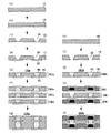
図1に本発明の多層配線基板200の製造方法の概略を示す。図1(a)〜(g)に示すように、本発明の多層配線基板200aは、熱可塑性樹脂組成物からなる絶縁基材10、この絶縁基材上に設けられた導体パターン20を備え、この絶縁基材10に導電性ペースト40が充填されたビアホール30が形成されてなる配線基板100aを、複数枚かさね合わせて、熱融着により積層して製造される。
Hereinafter, the present invention will be described based on embodiments shown in the drawings.
FIG. 1 shows an outline of a method for manufacturing a
また、本発明の別の形態の多層配線基板200bは、図1(h)〜(l)に示すように、熱可塑性樹脂からなる絶縁基材10を備え、この絶縁基材10に導電性ペースト40が充填されたビアホール30が形成されてなる配線基板100bを、この配線基板100bとは異なる熱可塑性樹脂組成物以外からなる配線基板300と交互に重ね合わせて、熱融着により積層して製造される。以下、本発明の多層配線基板200a、200bの各構成要素を順次説明する。
In addition, as shown in FIGS. 1H to 1L, a
<熱可塑性樹脂組成物からなる絶縁基材10>
熱可塑性樹脂組成物からなる絶縁基材10を形成する熱可塑性樹脂組成物としては、260℃以上の結晶融解ピーク温度(Tm)を有する、ポリアリールケトン樹脂および非晶性ポリエーテルイミド樹脂の混合組成物を用いることが好ましい。なお、ポリアリールケトン樹脂および非晶性ポリエーテルイミド樹脂は相溶系であり、これらの混合組成物は一つの結晶融解ピーク温度を有する。つまり、上記においては、ポリアリールケトン樹脂および非晶性ポリエーテルイミド樹脂の混合組成物が示す一つの結晶融解温度が260℃以上であることを意味している。
<Insulating
The thermoplastic resin composition forming the insulating
このポリアリールケトン樹脂は、その構造単位に芳香核結合、エーテル結合およびケトン結合を含む熱可塑性樹脂であり、その代表例としては、ポリエーテルケトン、ポリエーテルエーテルケトン、ポリエーテルケトンケトン等があり、なかでも、ポリエーテルエーテルケトンが好ましい。なお、ポリエーテルエーテルケトンは、「PEEK151G」、「PEEK381G」、「PEEK450G」(いずれもVICTREX社の商品名)等として市販されている。 This polyaryl ketone resin is a thermoplastic resin having an aromatic nucleus bond, an ether bond and a ketone bond in its structural unit, and representative examples include polyether ketone, polyether ether ketone, polyether ketone ketone, etc. Of these, polyetheretherketone is preferred. Polyether ether ketone is commercially available as “PEEK151G”, “PEEK381G”, “PEEK450G” (all are trade names of VICTREX), and the like.
また、非晶性ポリエーテルイミド樹脂は、その構造単位に芳香核結合、エーテル結合およびイミド結合を含む非晶性熱可塑性樹脂であり、特に制限されるものではない。なお、ポリエーテルイミドは、「Ultem CRS5001」、「Ultem 1000」(いずれもゼネラルエレクトリック社の商品名)等として市販されている。 The amorphous polyetherimide resin is an amorphous thermoplastic resin containing an aromatic nucleus bond, an ether bond and an imide bond in the structural unit, and is not particularly limited. Polyetherimide is commercially available as “Ultem CRS 5001”, “Ultem 1000” (both are trade names of General Electric).
ポリアリールケトン樹脂および非晶性ポリエーテルイミド樹脂の混合割合としては、積層する他の配線基板100、300との密着性を考慮した場合、ポリアリールケトン樹脂を30質量%以上かつ70質量%以下含有し、残部を非晶性ポリエーテルイミド樹脂および不可避不純物とした混合組成物を用いることが好ましい。ここで、ポリアリールケトン樹脂の含有率を30質量%以上かつ70質量%以下と限定した理由は、ポリアリールケトン樹脂の含有率が高すぎると、熱可塑性樹脂組成物の結晶性が高いために多層化する際の積層性が低下するからであり、また、ポリアリールケトン樹脂の含有率が低すぎると、熱可塑性樹脂組成物全体としての結晶性自体が低くなり、結晶融解ピーク温度が260℃以上であってもリフロー耐熱性が低下するからである。
The mixing ratio of the polyaryl ketone resin and the amorphous polyetherimide resin is 30% by mass or more and 70% by mass or less of the polyaryl ketone resin in consideration of adhesion to
この熱可塑性樹脂組成物は無機充填材を含有していてもよい。無機充填材としては、特に制限はなく、公知のいかなるものも使用できる。例えば、タルク、マイカ、雲母、ガラスフレーク、窒化ホウ素(BN)、板状炭カル、板状水酸化アルミニウム、板状シリカ、板状チタン酸カリウム等が挙げられる。これらは1種類を単独で添加してもよく、2種類以上を組み合わせて添加してもよい。特に、平均粒径が15μm以下、アスペクト比(粒径/厚み)が30以上の鱗片状の無機充填材が、平面方向と厚み方向の線膨張係数比を低く抑えることができ、熱衝撃サイクル試験時の基板内のクラック発生を抑制することができるので、好ましい。 This thermoplastic resin composition may contain an inorganic filler. There is no restriction | limiting in particular as an inorganic filler, Any well-known thing can be used. Examples thereof include talc, mica, mica, glass flake, boron nitride (BN), plate-like carbon cal, plate-like aluminum hydroxide, plate-like silica, and plate-like potassium titanate. These may be added singly or in combination of two or more. In particular, a scale-like inorganic filler having an average particle size of 15 μm or less and an aspect ratio (particle size / thickness) of 30 or more can keep the linear expansion coefficient ratio in the plane direction and the thickness direction low, and the thermal shock cycle test. This is preferable because generation of cracks in the substrate at the time can be suppressed.
この無機充填材の添加量は、熱可塑性樹脂100質量部に対して20質量部以上かつ50質量部以下が好ましい。無機充填材の添加量が多すぎると、無機充填材の分散不良の問題が発生し、線膨張係数がばらつき易くなったり、強度低下を招き易くなったりするからである。また、無機充填材の添加量が少なすぎると、線膨張係数を低下させて寸法安定性を向上させる効果が小さく、リフロー工程において他の配線基板300や導電パターン20との線膨張係数差に起因する内部応力が発生し、基板にそりやねじれが発生するからである。
The added amount of the inorganic filler is preferably 20 parts by mass or more and 50 parts by mass or less with respect to 100 parts by mass of the thermoplastic resin. This is because if the amount of the inorganic filler added is too large, a problem of poor dispersion of the inorganic filler occurs, and the linear expansion coefficient tends to vary or the strength tends to decrease. In addition, if the amount of the inorganic filler added is too small, the effect of reducing the linear expansion coefficient and improving the dimensional stability is small, which is caused by the difference in the linear expansion coefficient with the
また、熱可塑性樹脂組成物は、その性質を損なわない程度に、他の樹脂や無機充填材以外の各種添加剤、例えば、安定剤、紫外線吸収剤、光安定剤、核剤、着色剤、滑剤、難燃剤等を適宜含有していてもよい。これら無機充填材を含めた各種添加剤を添加する方法としては、公知の方法、例えば下記に挙げる方法(a)、(b)を用いることができる。 In addition, the thermoplastic resin composition has various additives other than other resins and inorganic fillers, such as a stabilizer, an ultraviolet absorber, a light stabilizer, a nucleating agent, a colorant, and a lubricant, to the extent that the properties are not impaired. In addition, flame retardants and the like may be appropriately contained. As a method of adding various additives including these inorganic fillers, a known method, for example, the following methods (a) and (b) can be used.
(a)各種添加剤を、ポリアリールケトン樹脂および/または非晶性ポリエーテルイミド樹脂の基材(ベース樹脂)に高濃度(代表的な含有量としては10〜60質量%程度)に混合したマスターバッチを別途作製しておき、これを使用する樹脂に濃度を調整して混合し、ニーダーや押出機等を用いて機械的にブレンドする方法。(b)使用する樹脂に直接各種添加剤をニーダーや押出機等を用いて機械的にブレンドする方法。これらの方法の中では、(a)の方法が分散性や作業性の点から好ましい。さらに、熱可塑性樹脂組成物からなる絶縁基材10の表面には積層性を向上させる目的でコロナ処理等を適宜施しても構わない。
(A) Various additives were mixed with a polyaryl ketone resin and / or an amorphous polyetherimide resin base material (base resin) at a high concentration (typically about 10 to 60% by mass). A method of preparing a master batch separately, adjusting the concentration of the master batch and mixing the resin, and mechanically blending it using a kneader or an extruder. (B) A method in which various additives are mechanically blended directly with a resin to be used using a kneader or an extruder. Among these methods, the method (a) is preferable from the viewpoint of dispersibility and workability. Further, the surface of the insulating
<導体パターン20>
導体パターン20は、熱可塑性樹脂組成物からなる絶縁基材10上に、金属箔を熱圧着等により貼り付けた後、エッチング処理して導体パターン20とする方法、熱可塑性樹脂組成物からなる絶縁基材10を押出製膜する際に金属箔に直接ラミネートする方法、あるいは、熱可塑性樹脂組成物からなる絶縁基材10上に、レジストを形成して、メッキにより導体パターン20を形成する方法、等の通常の回路パターンを作製する方法により形成することができる。なお、以下において説明するように、本発明における好ましい形態である熱可塑性樹脂組成物は、急冷製膜により非晶性フィルム化されているので、比較的低温において熱圧着することが可能である。導体パターン20を形成する金属としては、Au、Ag、Cu等の電気抵抗が小さい金属を使用することができる。この中でも、配線基板の導体パターンとして使用されてきた実績が豊富であること、コストが低いことから、Cuを使用することが好ましい。
<
The
<導電性ペースト組成物40>
熱可塑性樹脂組成物からなる絶縁基材10には、ビアホール30が形成され、この中に導電性ペースト組成物40が充填される。本発明の多層配線基板200において使用される導電性ペースト組成物40は、導電粉末、および、バインダー成分を含むものである。
<
A via
(導電粉末)
本発明において使用する導電粉末は、第1の合金粒子と第2の金属粒子とから構成されるものである。
(Conductive powder)
The conductive powder used in the present invention is composed of first alloy particles and second metal particles.
第1の合金粒子は、180℃以上260℃未満の融点を有する非鉛半田粒子である。このような非鉛半田粒子としては、例えば、Sn−Cu、Sn−Sb、Sn−Ag−Cu、Sn−Ag−Cu−Bi、Sn−Ag−In、Sn−Ag−In−Bi、Sn−Zn、Sn−Zn−Bi、および、Sn−Ag−Biを挙げることができる。これらの非鉛半田粒子は、錫を金属拡散させるという効果において信頼をおけるものである。また、第1の合金粒子としては、これらの非鉛半田粒子の二種以上の混合物を使用することもできる。 The first alloy particles are non-lead solder particles having a melting point of 180 ° C. or higher and lower than 260 ° C. Examples of such lead-free solder particles include Sn—Cu, Sn—Sb, Sn—Ag—Cu, Sn—Ag—Cu—Bi, Sn—Ag—In, Sn—Ag—In—Bi, and Sn—. Zn, Sn-Zn-Bi, and Sn-Ag-Bi can be mentioned. These lead-free solder particles are reliable in the effect of metal diffusion of tin. As the first alloy particles, a mixture of two or more of these non-lead solder particles can also be used.
第2の金属粒子は、Au、Ag、Cuからなる群から選ばれる少なくとも一種以上の金属粒子である。第2の金属粒子は、電気抵抗値が低い金属から形成されている粒子であり、ビアホールの電気伝導性を担うものである。また、第2の金属粒子は、第1の合金粒子に比べて融点が高く、加熱時における導電性ペースト組成物の粘度を保持する役割を有する。 The second metal particles are at least one or more metal particles selected from the group consisting of Au, Ag, and Cu. The second metal particle is a particle formed of a metal having a low electric resistance value, and bears the electric conductivity of the via hole. The second metal particles have a higher melting point than the first alloy particles, and have a role of maintaining the viscosity of the conductive paste composition during heating.
導電粉末における、第1の合金粒子および第2の金属粒子の混合割合は、質量比で、「76/24」以上「90/10」未満である(「第1の合金粒子」/「第2の金属粒子」)。この範囲を超えて、第1の合金粒子の量が多すぎると、基板を加熱積層する際に、導電性ペースト組成物の粘度の低下が大きく、導電性ペースト組成物40がビアホール30から流出してしまうおそれがある。
The mixing ratio of the first alloy particles and the second metal particles in the conductive powder is “76/24” or more and less than “90/10” by mass ratio (“first alloy particles” / “second” Metal particles "). If the amount of the first alloy particles is too large beyond this range, the viscosity of the conductive paste composition is greatly reduced when the substrate is heated and laminated, and the
第1の合金粒子および第2の金属粒子の平均粒子径は、10μm以下であることが好ましい。第1の合金粒子をこのような粒径とすることによって、導電性ペースト組成物40をビアホール30に充填しやすくなり、また、金属拡散が生じやすくなる。また、第2の金属粒子をこのような粒径とすることによって、基板を加熱積層する際における導電性ペースト組成物の粘度を調整する効果が良好となる。
The average particle diameter of the first alloy particles and the second metal particles is preferably 10 μm or less. By setting the first alloy particles to such a particle size, the
第1の合金粒子と第2の金属粒子の平均粒径差は、2μm以下であることが好ましい。このように粒径をなるべくそろえることによって、金属拡散接合を生じやすくすることができる。 The average particle size difference between the first alloy particles and the second metal particles is preferably 2 μm or less. By aligning the particle diameters as much as possible, metal diffusion bonding can be easily generated.
(バインダー成分)
本発明において使用するバインダー成分は、加熱により硬化する重合性単量体の混合物である。このようなバインダー成分としては、アルケニルフェノール化合物およびマレイミド類の混合物を挙げることができる。なお、アルケニルフェノール化合物および/またはマレイミド類が、高分子化合物であっても、これらを加熱することにより、架橋反応して硬化するものであれば、本発明の重合性単量体に含まれるものとする。
(Binder component)
The binder component used in the present invention is a mixture of polymerizable monomers that are cured by heating. Examples of such a binder component include a mixture of an alkenylphenol compound and maleimides. In addition, even if the alkenylphenol compound and / or maleimide is a polymer compound, it can be included in the polymerizable monomer of the present invention as long as it is cured by crosslinking reaction by heating. And
アルケニルフェノール化合物としては、分子中に少なくとも2個のアルケニル基を有するアルケニルフェノール化合物、つまり、芳香環の水素原子の一部がアルケニル基に置換されたフェノール系化合物を挙げることができる。また、具体的には、このようなアルケニルフェノール化合物としては、ビスフェノールAまたはフェノール性水酸基含有ビフェニル骨格にアルケニル基が結合した化合物を挙げることができる。さらに具体的には、3,3´−ビス(2−プロペニル)−4,4´−ビフェニルジオール、3,3´−ビス(2−プロペニル)−2,2´−ビフェニルジオール、3,3´−ビス(2−メチル−2−プロペニル)−4,4´−ビフェニルジオール、3,3´−ビス(2−メチル−2−プロペニル)−2,2´−ビフェニルジオール等のジアルケニルビフェニルジオール化合物;2,2−ビス[4−ヒドロキシ−3−(2−プロペニル)フェニル]プロパン、2,2−ビス[4−ヒドロキシ−3−(2−メチル−2−プロペニル)フェニル]プロパン(以下、「ジメタリルビスフェノールA」と云う。)等のジアルケニルビスフェノール化合物を挙げることができる。この中でも、原料コストが安く、安定供給が可能であるという点から、アルケニルフェノール化合物としては、ジメタリルビスフェノールAを使用することが好ましい。ジメタリルビスフェノールAの構造式を式1に示す。
Examples of the alkenylphenol compound include alkenylphenol compounds having at least two alkenyl groups in the molecule, that is, phenolic compounds in which a part of the hydrogen atoms of the aromatic ring are substituted with alkenyl groups. Specifically, examples of such alkenylphenol compounds include compounds in which an alkenyl group is bonded to bisphenol A or a phenolic hydroxyl group-containing biphenyl skeleton. More specifically, 3,3′-bis (2-propenyl) -4,4′-biphenyldiol, 3,3′-bis (2-propenyl) -2,2′-biphenyldiol, 3,3 ′ Dialkenyl biphenyldiol compounds such as -bis (2-methyl-2-propenyl) -4,4'-biphenyldiol and 3,3'-bis (2-methyl-2-propenyl) -2,2'-biphenyldiol 2,2-bis [4-hydroxy-3- (2-propenyl) phenyl] propane, 2,2-bis [4-hydroxy-3- (2-methyl-2-propenyl) phenyl] propane (hereinafter “ And dialkenyl bisphenol compounds such as “dimethallyl bisphenol A”). Among these, it is preferable to use dimethallyl bisphenol A as the alkenylphenol compound from the viewpoint that the raw material cost is low and stable supply is possible. The structural formula of dimethallylbisphenol A is shown in

マレイミド類としては、分子中に少なくとも2個のマレイミド基を有するマレイミド化合物を挙げることができ、具体的には、ビス(4−マレイミドフェニル)メタン等のビスマレイミド、トリス(4−マレイミドフェニル)メタン等のトリスマレイミド、ビス(3,4−ジマレイミドフェニル)メタン等のテトラキスマレイミドおよびポリ(4−マレイミドスチレン)等のポリマレイミド等を挙げることができる。この中でも、マレイミド類としては、原料コストが安く、安定供給が可能であるという点から、ビス(4−マレイミドフェニル)メタンを使用することが好ましい。ビス(4−マレイミドフェニル)メタンの構造式を式2に示した。 Examples of maleimides include maleimide compounds having at least two maleimide groups in the molecule. Specific examples thereof include bismaleimides such as bis (4-maleimidophenyl) methane and tris (4-maleimidophenyl) methane. And trismaleimide such as bis (3,4-dimaleimidophenyl) methane, and polymaleimide such as poly (4-maleimidostyrene). Among these, as maleimides, it is preferable to use bis (4-maleimidophenyl) methane because raw material costs are low and stable supply is possible. The structural formula of bis (4-maleimidophenyl) methane is shown in Formula 2.
このバインダー成分において、アルケニルフェノール化合物およびマレイミド類の混合比は、モル比で、「30/70」以上「70/30」未満であることが好ましい(「アルケニルフェノール化合物」/「マレイミド類」)。この範囲を超えて、バインダー成分中のどちらかの成分が多すぎると、生成する樹脂が脆くなり、導電性ペースト組成物40と導体パターン20部との接着力が低下してしまう。
In this binder component, the molar ratio of the alkenylphenol compound and maleimide is preferably “30/70” or more and less than “70/30” (“alkenylphenol compound” / “maleimides”). If this range is exceeded and either component in the binder component is too much, the resulting resin becomes brittle and the adhesive strength between the
バインダー成分の硬化反応について、以下説明する。アルケニルフェノール化合物におけるアルケニル基は、マレイミド化合物のエチレン性不飽和基と交互共重合および/または付加反応し、またフェノール性水酸基もマレイミド基のエチレン性不飽和基と付加反応する。以下、バインダー成分として例示した、ジメタリルビスフェノールAおよびビス(4−マレイミドフェニル)メタンの硬化機構について、具体的に説明する。まず、120〜180℃に加熱した段階で、以下の式3で示される線状の重合体が得られる。 The curing reaction of the binder component will be described below. The alkenyl group in the alkenylphenol compound undergoes alternating copolymerization and / or addition reaction with the ethylenically unsaturated group of the maleimide compound, and the phenolic hydroxyl group also undergoes addition reaction with the ethylenically unsaturated group of the maleimide group. Hereinafter, the curing mechanism of dimethallylbisphenol A and bis (4-maleimidophenyl) methane exemplified as the binder component will be specifically described. First, in the stage heated to 120-180 degreeC, the linear polymer shown by the following formula | equation 3 is obtained.
さらに、200℃以上に加熱すると、例えば、以下の式4で示される三次元状に架橋した重合体が得られる。 Furthermore, when heated to 200 ° C. or higher, for example, a three-dimensionally crosslinked polymer represented by the following formula 4 is obtained.
本発明においては、このようなバインダー成分の三次元架橋による硬化が、半田成分が第2の金属粒子および/または導体パターン20を形成する金属へ金属拡散することを促進し、これにより高度な金属拡散接合が形成されると考えられている。つまり、バインダー成分が硬化する時に、ビアホール30内の第1の合金粒子および第2の金属粒子に圧力がかかり、これにより、半田成分が、金属粒子および導体パターン20を形成する金属へ金属拡散することが促進されると考えられている。バインダー成分の弾性率が、温度によって変化する様子を図2に示す。単量体混合物の弾性率は、温度の上昇により小さくなっていく。しかし、120〜180℃において式3で示した線状の重合体が形成されることによって、弾性率が急に大きくなる(図2における、「単量体混合物」のグラフから、「架橋後」のグラフとなる。)。その後、線状の重合体は、200℃以上において、式4で示される三次元状に架橋した重合体に変化していくと考えられている。架橋後のグラフは、温度の上昇と共に小さくなる傾向はある。しかし、高温領域においても溶融することなく、一定の弾性率を保っている。
In the present invention, the curing by the three-dimensional crosslinking of the binder component promotes the metal diffusion of the solder component to the metal forming the second metal particles and / or the
このように、180〜260℃において非鉛半田粒子が融解した時に、バインダー成分は硬化反応することにより、一定の弾性率を保持する。このように、融解した非鉛半田粒子に対して、バインダーが硬化することによる圧力がかかり、これにより、導電性ペースト組成物40において、金属拡散接合が生じると考えられる。そして、このような導電性ペースト組成物40を用いた、本発明の多層配線基板200は、そのビアホールの抵抗値が非常に低いものとなり、吸湿耐熱性、接続信頼性、および、導体接着強度に優れたものになると考えられる。
Thus, when the lead-free solder particles are melted at 180 to 260 ° C., the binder component undergoes a curing reaction to maintain a certain elastic modulus. As described above, it is considered that the molten lead-free solder particles are subjected to pressure due to the binder being cured, and thereby, metal diffusion bonding occurs in the
このような観点から、半田粒子が溶解した段階で、バインダー成分が硬化する必要があり、非鉛半田粒子の融点が、バインダー成分の硬化温度範囲に含まれている必要がある。これに対して、バインダー成分の硬化温度範囲に比べて、非鉛半田粒子の融点が高すぎる場合は、バインダー成分が硬化する段階において、非鉛半田粒子は未だ融解していないため、金属拡散が促進されるという効果を享受することができない。また、バインダー成分の硬化温度範囲に比べて、非鉛半田粒子の融点が低すぎる場合は、溶解した半田成分がビアホールからはみ出してしまうおそれがある。 From such a viewpoint, the binder component needs to be cured at the stage where the solder particles are dissolved, and the melting point of the lead-free solder particles needs to be included in the curing temperature range of the binder component. On the other hand, when the melting point of the lead-free solder particles is too high compared to the curing temperature range of the binder component, the lead-free solder particles are not yet melted at the stage where the binder component is cured. The effect of being promoted cannot be enjoyed. In addition, when the melting point of the non-lead solder particles is too low as compared with the curing temperature range of the binder component, the dissolved solder component may protrude from the via hole.
なお、バインダー成分の硬化温度範囲は、昇温速度10℃/分における示差走査熱量測定(DSC)により測定した発熱ピークの発生温度により、測定した。 In addition, the curing temperature range of the binder component was measured by the generation temperature of an exothermic peak measured by differential scanning calorimetry (DSC) at a temperature rising rate of 10 ° C./min.
上記したように、導電性ペースト組成物40は、導電粉末およびバインダー成分を含有するものであるが、この導電粉末およびバインダー成分の混合比は、質量比で、「90/10」以上「98/2」未満である(「導電性粉末」/「バインダー成分」)。この範囲を超えて、導電性粉末の量が少なすぎるとビアホールに充填した導電性ペーストの電気抵抗値が増加してしまう。また、この範囲を超えて、導電性粉末の量が多すぎると、導電性ペースト組成物40をビアホール30に印刷充填する作業性が悪化し、また、導電性ペースト組成物40と導体パターン20部との接着強度が低下してしまう。
As described above, the
<熱可塑性樹脂組成物以外からなる配線基板300>
熱可塑性樹脂組成物以外からなる配線基板300としては、ガラスエポキシ基板(FR4基板)、2層ポリイミド基板、擬似2層ポリイミド基板、3層ポリイミド基板、液晶ポリマー(LCP)基板、低温焼成セラミック(LTCC)基板を使用することができる。これらの配線基板300は、二種以上を併せて積層して多層基板200を形成してもよい。
<
The
ガラスエポキシ基板(FR4基板)の製造方法について説明する。まず、ガラスクロスに熱硬化性樹脂を含浸させ半硬化状態(Bステージ化)とした絶縁基材(プリブレグ)を用意する。次いで、絶縁基材の所定位置に、レーザー若しくは機械ドリル等を用いて絶縁基材を貫通する貫通孔を形成し、これをビアホールとする。次いで、スクリーン印刷等によりビアホール内に導電性ペーストを充填する。そして、必要により、加熱して溶剤を揮発させて導電性ペーストを固化させる。配線基板300に用いられる導電性ペーストとしては、特に限定されず、ビアホール充填用に使用される一般的な導電性ペーストを使用することができる。また、配線基板300に用いられる導電性ペーストとして、配線基材100において使用する導電性ペースト組成物40を使用することもできる。次いで、必要に応じて、絶縁基材の表面上にはみ出した導電性ペーストの乾燥固化物を機械的研磨等により除去して、そして、絶縁基材の一方の面あるいは両方の面に、銅箔を熱圧着すると同時に絶縁基材を完全に硬化する(Cステージ化)。次いで、銅箔をエッチングによりパターニングし、導体パターンを形成する。以上より、ガラスエポキシ基板を使用した熱可塑性樹脂組成物以外からなる配線基板300を製造することができる。
A method for manufacturing a glass epoxy substrate (FR4 substrate) will be described. First, an insulating base material (prepreg) in which a glass cloth is impregnated with a thermosetting resin to form a semi-cured state (B stage) is prepared. Next, a through-hole penetrating the insulating base material is formed at a predetermined position of the insulating base material using a laser or a mechanical drill, and this is used as a via hole. Next, a conductive paste is filled into the via hole by screen printing or the like. Then, if necessary, the conductive paste is solidified by heating to volatilize the solvent. The conductive paste used for the
上記したエポキシ樹脂の「Bステージ」とは、樹脂、硬化剤を混合した場合において、反応がある程度進んだ、半硬化(Semi−cure)の状態をいう。この段階では、もはや大部分は溶剤に溶解しないが、加熱すると溶解してさらに反応が進む。また、「Cステージ」とは、反応の最終段階で不溶不融の完全硬化の状態をいう。 The “B stage” of the above-described epoxy resin refers to a semi-cured state in which the reaction proceeds to some extent when the resin and the curing agent are mixed. At this stage, most of it is no longer dissolved in the solvent, but when heated, it dissolves and the reaction proceeds further. The “C stage” refers to a completely cured state that is insoluble and infusible at the final stage of the reaction.
また、液晶ポリマー(LCP)基板の製造方法について説明する。まず、LCPからなる絶縁基板を用意する。LCPとしては、LCPI型(液晶転移温度:350℃)、LCPII型(液晶転移温度:300℃)等を使用することができる。LCPからなる絶縁基材としては、フィルム状、薄板状、またはシート状が好ましい。その成形方法としては、公知の方法、例えばTダイを用いる押出キャスト法、あるいはカレンダー法、インフレーション成形法等が好ましく、特に限定されるものではないが、シートの製膜性や安定生産性等を考慮すると、Tダイを用いる押出キャスト法が好ましい。Tダイを用いる押出キャスト法での成形温度は、用いる樹脂の流動性や製膜性等によって適宜調整されるが、概ね、LCPI型樹脂の場合、400〜420℃、LCPII型樹脂の場合、350〜370℃である。製膜時に銅箔を貼り付け、その後、絶縁基材にビアホールを形成し、パターニングして導体パターンを形成することについては、上記したガラスエポキシ基板の製造方法における場合と同様である。 A method for manufacturing a liquid crystal polymer (LCP) substrate will be described. First, an insulating substrate made of LCP is prepared. As the LCP, LCPI type (liquid crystal transition temperature: 350 ° C.), LCP II type (liquid crystal transition temperature: 300 ° C.), or the like can be used. As the insulating substrate made of LCP, a film shape, a thin plate shape, or a sheet shape is preferable. The molding method is preferably a known method, for example, an extrusion casting method using a T die, a calendar method, an inflation molding method, or the like, and is not particularly limited. Considering, an extrusion casting method using a T die is preferable. The molding temperature in the extrusion casting method using a T-die is appropriately adjusted depending on the fluidity and film-forming property of the resin used, but is generally 400 to 420 ° C. for the LCPI type resin and 350 for the LCP II type resin. ~ 370 ° C. The copper foil is affixed at the time of film formation, and then a via hole is formed in the insulating base material and patterned to form a conductor pattern, which is the same as in the above-described method for manufacturing a glass epoxy substrate.
銅箔上にキャスト法や流延法でポリイミド層を形成した2層ポリイミド基板や、ポリイミドフィルムと銅箔間に熱可塑性ポリイミド層を接着層として熱ラミネートした擬似2層ポリイミド基板や、ポリイミドフィルムと銅箔間に熱硬化型の接着剤を用いた3層ポリイミド基板についても、上記したガラスエポキシ基板、LCP基板と同様の製造方法により製造することができる。 A two-layer polyimide substrate in which a polyimide layer is formed on a copper foil by a casting method or a casting method, a pseudo two-layer polyimide substrate in which a thermoplastic polyimide layer is bonded as an adhesive layer between a polyimide film and a copper foil, and a polyimide film A three-layer polyimide substrate using a thermosetting adhesive between copper foils can also be manufactured by the same manufacturing method as the above-described glass epoxy substrate and LCP substrate.
LTCC(低温焼成セラミック)基板は、焼成前のLTCC(低温焼成セラミック)基板にビアホールを形成し、ビアホール中にAgペーストを充填し、また表層にもAgペースト配線を施し、焼成して作製した。 The LTCC (low temperature fired ceramic) substrate was produced by forming via holes in an LTCC (low temperature fired ceramic) substrate before firing, filling the via holes with Ag paste, and applying Ag paste wiring to the surface layer and firing.
<熱可塑性樹脂組成物からなる絶縁基材10を備えた配線基板100aの製造方法>
図1(a)〜(e)に、単層の配線基板100aを製造する工程を示した。まず、図1(a)に示すように、熱可塑性樹脂組成物からなる絶縁基材10を用意する。絶縁基材10は、フィルム、薄板状またはシート状が好ましく、成形方法としては、公知の方法、例えばTダイを用いる押出キャスト法、あるいはカレンダー法等を採用することができ、特に限定されるものではないが、シートの製膜性や安定生産性等の点から、Tダイを用いる押出キャスト法が好ましい。Tダイを用いる押出キャスト法での成形温度は、用いる樹脂の流動特性や製膜性等によって適宜調整されるが、概ね、260℃以上の結晶融解ピーク温度を有する、ポリアリールケトン樹脂および非晶性ポリエーテルイミド樹脂の混合組成物の場合、360〜400℃である。また、押出キャスト製膜時に急冷製膜することにより非晶性フィルム化することが必要である。これにより、170〜230℃付近に弾性率が低下する領域を発現するので、この温度領域での熱成形、熱融着が可能となる。詳細には、170℃付近で弾性率が低下し始め、200℃付近において熱成形、熱融着が可能となる。また、図3に示したグラフは、昇温速度を3℃/分として弾性率を測定したものであるが、昇温速度を10℃/分とすると、非晶から結晶への転移が遅れて、230℃付近において弾性率がもっとも低くなる。
<The manufacturing method of the
1A to 1E show a process for manufacturing a single-
次いで、図1(b)に示すように、熱可塑性樹脂組成物からなる絶縁基材10の表面に金属箔が貼り付けられる。上記したように熱可塑性樹脂組成物からなる絶縁基材10は非晶性の状態であるため、熱可塑性樹脂の結晶化が大きく進行しないガラス転移温度の少し上の温度での比較的短時間での熱圧着により、絶縁基材の結晶化を進行させずに金属箔を貼り付けることができる。また、絶縁基材10を製膜する際に銅箔を同時にラミネートして図1(b)の段階にしても良い。
Subsequently, as shown in FIG.1 (b), metal foil is affixed on the surface of the insulating
次いで、図1(c)に示すように、絶縁基材10の所定位置に、レーザー若しくは機械ドリル等を用いてビアホール30が形成される。次いで、図1(d)に示すように、金属箔の表面にレジストを回路パターン状に塗布して、エッチング、レジスト除去する等の通常の方法により、導体パターン20が形成される。なお、ビアホールを形成してから、銅箔を貼り付けて、導体パターン20を形成してもよいし、導体パターン20を形成してから、ビアホールを形成してもよく、各手順の順序は特に限定されない。次いで、ビアホール30に、スクリーン印刷等の通常の印刷手法によって、導電性ペースト組成物40が充填され、図1(e)に示すような単層の配線基板100aが作製される。
Next, as shown in FIG. 1C, a via
<熱可塑性樹脂組成物からなる絶縁基材10の温度に対する弾性率の挙動>
ここで、熱可塑性樹脂組成物からなる絶縁基材10の温度に対する弾性率の挙動について説明する。熱可塑性樹脂組成物として、260℃以上の結晶融解ピーク温度(Tm)を有する、ポリアリールケトン樹脂および非晶性ポリエーテルイミド樹脂の混合組成物であって、特に、ポリアリールケトン樹脂としてポリエーテルエーテルケトンを使用した場合における絶縁基材10の、温度に対する弾性率の挙動を図3に示した。
<Behavior of elastic modulus with respect to temperature of insulating
Here, the behavior of the elastic modulus with respect to the temperature of the insulating
「積層前」と表示されているのが、多層配線基板200として積層する前における、絶縁基材10の温度に対する弾性率の挙動を示したグラフである。また、「積層後」と表示されているのが、所定の条件において加熱・加圧することによって多層配線基板200とした後における、絶縁基材10の温度に対する弾性率の挙動を示したグラフである。積層前の状態では、上記したように、絶縁基材10は急冷製膜することにより非晶性フィルム化されている。よって、200℃付近という比較的低温領域において弾性率が十分に低下する。これにより、積層前の絶縁基材10は、比較的低温において熱成形、熱融着することができる。
“Before lamination” is a graph showing the behavior of the elastic modulus with respect to the temperature of the insulating
非晶性フィルム化されている絶縁基材10は、多層配線基材200を製造する際における所定の条件下での加熱・加圧成形によって、結晶性へと変化する。これに伴って絶縁基材10の弾性率は大きく変化して、図3における積層後のグラフで示されるような挙動を示すようになる。これにより、以下に説明するように金属拡散接合を促進するという効果を発揮して、本発明の多層配線基板200を、そのビアホールの抵抗値を非常に小さくすることができると共に、吸湿耐熱性、接続信頼性、および導体接着力に優れたものとすることができると考えられている。
The insulating
次に、どのように金属拡散接合が促進されるかについて説明する。ここで、導電性ペースト組成物40中の非鉛半田粒子と熱可塑性樹脂組成物からなる絶縁基材10との関係が重要であり、非鉛半田粒子の融点における、熱可塑性樹脂組成物の貯蔵弾性率は、10MPa以上5GPa未満であることが好ましい。なお、熱可塑性樹脂組成物からなる絶縁基材10を形成する熱可塑性樹脂組成物として、上記した好ましい形態である、ポリエーテルエーテルケトンおよび非晶性ポリエーテルイミドの混合組成物を使用した場合は、図3に示すように、180℃以上260℃未満という非鉛半田粒子の融点における、熱可塑性樹脂組成物の貯蔵弾性率は、10MPa以上5GPa未満となっている。なお、熱可塑性樹脂組成物の貯蔵弾性率は、粘弾性評価装置を用い、測定周波数1Hzで昇温速度3℃/分で測定した値である。
Next, how metal diffusion bonding is promoted will be described. Here, the relationship between the lead-free solder particles in the
上記のように非鉛半田粒子の融点において、熱可塑性樹脂組成物が10MPa以上5GPa未満の貯蔵弾性率を有するものとすることは、非鉛半田粒子の融点において、熱可塑性樹脂組成物にある程度の柔軟性を持たせると共に、溶融せずにある程度の弾性率を保持させていることを意味している。 As described above, the thermoplastic resin composition has a storage elastic modulus of 10 MPa or more and less than 5 GPa at the melting point of the lead-free solder particles. It means that a certain degree of elastic modulus is maintained without being melted while having flexibility.
このように、非鉛半田粒子の融点において、熱可塑性樹脂組成物にある程度の柔軟性を持たせることによって、導電性ペースト組成物40と熱可塑性樹脂組成物とが相互になじむことができ、導電性ペースト組成物40と熱可塑性樹脂組成物からなる絶縁基材10との接着性が向上する。また、非鉛半田粒子の融点において、熱可塑性樹脂組成物が溶融せずに、ある程度の弾性率を保持することによって、配線基板100を熱融着により積層する際に、導電性ペースト組成物40をビアホールの側面である熱可塑性樹脂組成物により締め付けることができ、導電性ペースト組成物40に圧力をかけることができる。これにより、非鉛半田粒子中の錫成分が第2の金属粒子および/または導体パターン20を形成する金属中に金属拡散し、金属拡散接合を形成させることができると考えられている。
Thus, by giving the thermoplastic resin composition a certain degree of flexibility at the melting point of the lead-free solder particles, the
<本発明の多層配線基板200の製造方法>
図1(e)〜(g)に、本発明の多層配線基板200aの製造工程を示した。図1(f)に示すように、作製した単層の配線基板100aを複数枚重ね合わせる。図示した形態においては、単層配線基板100aを三つ重ね合わせている。また、最下層の基板をその方向を変えて重ね合わせて、多層基板の外側に導体パターン20が形成されるようにしている。具体的には、図4に示すように、ヒーター内蔵の積層治具50内に下側より弾性および離型性を有するクッションフィルム51、配線基材100aを三つ、その上に、クッションフィルム51を重ねて、その後、押圧治具52を、図中に示した矢印の方向に押し下げることで、三つの配線基材100aに熱圧着を施し、これらを積層一体化して本発明の多層配線基板200aを製造する。各層の積層条件としては、金属拡散接合を効果的に起こらしめる観点から、温度:200℃以上260℃未満、圧力:3MPa以上8MPa未満、プレス時間:10分以上40分未満とすることが好ましい。
<Method for Manufacturing
1E to 1G show the manufacturing process of the
図1(h)〜(l)は、熱可塑性樹脂組成物からなる絶縁基材10を備えた配線基板100b、および、熱可塑性樹脂組成物以外からなる配線基板300を交互に重ね合わせて、本発明の多層配線基板200bを製造する工程を示した図である。まず、図1(h)に示すように、熱可塑性樹脂組成物からなる絶縁基材10を用意する。成形方法については、図1(a)の場合と同様である。次いで、図1(i)に示すように、絶縁基材10の所定位置に、レーザー若しくは機械ドリル等を用いてビアホール30が形成される。そして、スクリーン印刷等の通常の印刷手法によって、形成されたビアホール30に導電性ペースト組成物40が充填され、図1(j)に示すような単層の配線基板100bが製造される。
1 (h) to 1 (l) show a circuit board in which a
次いで、図1(k)に示すように、製造した単層の配線基板100bと、この配線基板100bとは異なる熱可塑性樹脂組成物以外からなる配線基板300とを交互に重ね合わせる。図示した形態においては、配線基板100bを真ん中にして、その両側に、熱可塑性樹脂以外からなる配線基板300が配置されている。
Next, as shown in FIG. 1 (k), the manufactured single-
そして、所定の条件において、各層が熱融着され、図1(l)に示すように本発明の多層配線基板200bが作製される。積層方法、積層条件は、上記の図1(g)において示した方法、条件と同様である。
Then, under the predetermined conditions, the layers are heat-sealed, and the
なお、図1(a)〜(g)に示した製造方法においては、単層配線基板100aの片面に導体パターン20を形成しており、また、図1(h)〜(l)に示した製造方法においては、単層配線基板100bに導体パターン20を形成せずに、熱可塑性樹脂組成物以外からなる配線基板300の両面に導体パターン20を形成しているが、製造する多層配線基板200a、200bにおいて所望の位置に導体パターン20が形成されるのであれば、単層配線基板100a、100b、300における導体パターンを形成する箇所は特に限定されず、適宜変更することができる。
In addition, in the manufacturing method shown to Fig.1 (a)-(g), the
<実施例1>
(絶縁基材10の作製)
ポリエーテルエーテルケトン樹脂(PEEK450G、Tm=335℃)40質量%と、非晶性ポリエーテルイミド樹脂(Ultem 1000)60質量%とからなる樹脂混合物100質量部に対して、平均粒径5μm、平均アスペクト比50の合成マイカを39質量部混合して得られた熱可塑性樹脂組成物を溶融混練し、急冷製膜して100μm厚の非晶性フィルムからなる絶縁基材10を作製した。この非晶性フィルムを、示差走査熱量計を用いて10℃/分で昇温させながら測定した時の結晶融解ピーク温度(Tm)は、335℃であった。
<Example 1>
(Preparation of insulating substrate 10)
For 100 parts by mass of a resin mixture composed of 40% by mass of a polyether ether ketone resin (PEEK450G, Tm = 335 ° C.) and 60% by mass of an amorphous polyetherimide resin (Ultem 1000), an average particle diameter of 5 μm and an average A thermoplastic resin composition obtained by mixing 39 parts by mass of synthetic mica having an aspect ratio of 50 was melt-kneaded and rapidly cooled to form an insulating
(ビアホール充填用導電性ペースト組成物の作製)
Sn−Ag−Cu合金粒子(平均粒径5.55μm、融点220℃、Sn:Ag:Cu(質量比)=96.5:3:0.5)76質量%およびCu粒子(平均粒径5μm)24質量%の割合で混合した導電粉末97質量部に対して、ジメタリルビスフェノールA50質量%およびビス(4−マレイミドフェニル)メタン50質量%の割合で混合した重合性単量体の混合物3質量部、ならびに溶剤としてγブチロラクトン7.2質量部、を添加して、3本ロールで混練して導電性ペースト組成物を調製した。
(Preparation of conductive paste composition for via hole filling)
Sn-Ag-Cu alloy particles (average particle size 5.55 μm, melting point 220 ° C., Sn: Ag: Cu (mass ratio) = 96.5 : 3: 0.5) 76% by mass and Cu particles (average particle size 5 μm) ) 3 mass of a mixture of polymerizable monomers mixed at a ratio of 50 mass% of dimethallylbisphenol A and 50 mass% of bis (4-maleimidophenyl) methane with respect to 97 mass parts of the conductive powder mixed at a ratio of 24 mass%. And 7.2 parts by mass of γ-butyrolactone as a solvent were added and kneaded with three rolls to prepare a conductive paste composition.
(単層の配線基板100aの作製)
205℃、5MPa、10分間の熱圧着により、12μmの厚みの銅箔を上記で作製した絶縁基材10に貼り付けた。次いで、絶縁基材の所望の位置に、レーザーを使用して絶縁基材を貫通する直径100μmのビアホールを形成した。そして、上記で調製した導電性ペースト組成物を、このビアホールにスクリーン印刷により充填した。充填後、125℃、45分間加熱し、溶剤を揮発させて導電性ペーストを乾燥固化した。その後、フォトリソグラフ法によって、銅箔に導体パターンを形成して、単層の配線基板100aを作製した。
(Production of single-
A copper foil having a thickness of 12 μm was attached to the insulating
(多層配線基板200aの作製)
上記で得られ単層の配線基板100aを3枚用意し、ビア部の位置が合うように積み重ね、温度230℃、5MPa、30分間、真空プレスすることにより積層して、絶縁基材10が結晶化した層厚0.3mmの3層の多層配線基板200aを作製した。
(Preparation of
Three single-
<実施例2>
実施例1において導電性ペースト組成物中の導電粉末を95質量部、重合性単量体の混合物を5質量部とした以外は、実施例1と同様にして、導電性ペースト組成物を調製し、単層の配線基板100aおよび多層配線基板200aを作製した。
<Example 2>
A conductive paste composition was prepared in the same manner as in Example 1 except that the conductive powder in the conductive paste composition in Example 1 was 95 parts by mass and the mixture of polymerizable monomers was 5 parts by mass. A single-
<実施例3>
実施例1において導電性ペースト組成物中の導電粉末を、Sn−Ag−Cu合金粒子85質量%、Cu粒子15質量%の割合で混合したものとした以外は、実施例1と同様にして、導電性ペースト組成物を調製し、単層の配線基板100aおよび多層配線基板200aを作製した。
<Example 3>
In the same manner as in Example 1 except that the conductive powder in the conductive paste composition in Example 1 was mixed at a ratio of 85% by mass of Sn—Ag—Cu alloy particles and 15% by mass of Cu particles, A conductive paste composition was prepared to produce a single-
<実施例4>
(単層の配線基板100bの作製)
実施例1において、絶縁基材10に銅箔を貼り付けない以外は、実施例1と同様にして単層の配線基板100bを作製した。
(ガラスエポキシ基板(FR4)の作製)
ガラスクロスにエポキシ樹脂組成物を含浸させて、厚さ100μmの半硬化状態(Bステージ)のプリプレグを用意した。このプリプレグの所定の箇所にレーザーによりビアホールを形成し、このビアホールに実施例1において調製した導電性ペースト組成物をスクリーン印刷により充填した。充填後、125℃45分間加熱し、溶剤を揮発させて導電性ペーストを乾燥固化した。
そして、プリプレグの両面に12μmの厚さの銅箔を180℃、5MPa、30分間の熱圧着により貼り付け、これと同時にエポキシ樹脂を完全に硬化した(Cステージ)。次いで、フォトリソグラフ法によって、銅箔に導体パターンを形成して、ガラスエポキシ基板を作製した。
(多層配線基板200bの作製)
上記で得られ単層の配線基板100bを1枚、および、ガラスエポキシ基板を2枚用意して、これらを交互に、ビア部の位置が合うように積み重ね、温度230℃、5MPa、30分間、真空プレスすることにより積層して、絶縁基材10が結晶化した層厚0.3mmの3層の多層配線基板200bを製造した。
<Example 4>
(Production of single-
In Example 1, a single-
(Production of glass epoxy substrate (FR4))
A glass cloth was impregnated with an epoxy resin composition to prepare a semi-cured (B stage) prepreg having a thickness of 100 μm. Via holes were formed by laser at predetermined locations of the prepreg, and the conductive paste composition prepared in Example 1 was filled into the via holes by screen printing. After filling, the conductive paste was dried and solidified by heating at 125 ° C. for 45 minutes to evaporate the solvent.
Then, a 12 μm thick copper foil was attached to both surfaces of the prepreg by thermocompression bonding at 180 ° C. and 5 MPa for 30 minutes, and at the same time, the epoxy resin was completely cured (C stage). Next, a conductive pattern was formed on the copper foil by a photolithographic method to produce a glass epoxy substrate.
(Preparation of
Prepare one single-
<実施例5>
実施例4において、ガラスエポキシ基板の代わりに、液晶ポリマー基板を用いた以外は、実施例4と同様にして、多層配線基板200bを製造した。液晶ポリマー基板の製造方法を以下に説明する。
(液晶ポリマー基板の製造方法)
Tダイを用いた押出キャスト法によって、LCPI型を420℃にて押し出すと同時に、12μmの厚さの銅箔を両面に貼り付けた。その後、上記のガラスエポキシ基板における場合と同様にして、ビアホールを形成し、導電性ペースト組成物を充填・乾燥し、導体パターンを形成して、厚さ0.1mmの液晶ポリマー基板を得た。
<Example 5>
In Example 4, a
(Manufacturing method of liquid crystal polymer substrate)
The LCPI mold was extruded at 420 ° C. by an extrusion casting method using a T die, and at the same time, a copper foil having a thickness of 12 μm was attached to both sides. Thereafter, in the same manner as in the above glass epoxy substrate, a via hole was formed, and the conductive paste composition was filled and dried to form a conductor pattern, thereby obtaining a liquid crystal polymer substrate having a thickness of 0.1 mm.
<実施例6>
実施例4において、ガラスエポキシ基板の代わりに、3層ポリイミド基板を用いた以外は、実施例4と同様にして、多層配線基板200bを得た。3層ポリイミド基板の製造方法を以下に説明する。
(3層ポリイミド基板の製造方法)
35μmのポリイミドフィルムの両面に、熱硬化型の接着層を薄くコーティングし、接着層の硬化が進まない程度に乾燥固化させ、この接着層付きポリイミドフィルムの所定の箇所にビアホールを形成し、このビアホールに実施例1において調製した導電性ペースト組成物をスクリーン印刷により充填した。充填後、さらに、接着層の硬化が進まない125℃45分間の条件で加熱乾燥し、溶剤を揮発させて導電性ペーストを乾燥固化した。
そして、ビアが形成された接着層付きポリイミドフィルムの両面に12μmの厚さの銅箔を180℃、5MPa、30分間の熱圧着により貼り付け、これと同時にエポキシ樹脂を完全に硬化した(Cステージ)。次いで、フォトリソグラフ法によって、銅箔に導体パターンを形成して、厚さ60μmの3層ポリイミド両面基板を作製した。
<Example 6>
In Example 4, a
(Method for producing a three-layer polyimide substrate)
A thermosetting adhesive layer is thinly coated on both sides of a 35 μm polyimide film, dried and solidified to such an extent that the adhesive layer does not cure, and a via hole is formed in a predetermined portion of the polyimide film with the adhesive layer. The conductive paste composition prepared in Example 1 was filled by screen printing. After filling, the conductive paste was further dried by heating under conditions of 125 ° C. and 45 minutes at which the adhesive layer did not cure, and the solvent was evaporated.
Then, a 12 μm thick copper foil was attached to both sides of the polyimide film with an adhesive layer on which vias were formed by thermocompression bonding at 180 ° C. and 5 MPa for 30 minutes, and at the same time, the epoxy resin was completely cured (C stage). ). Next, a conductor pattern was formed on the copper foil by a photolithographic method to produce a three-layer polyimide double-sided substrate having a thickness of 60 μm.
<実施例7>
実施例4において、ガラスエポキシ基板の代わりに、LTCCを用いた以外は、実施例4と同様にして、多層配線基板200bを得た。LTCCの製造方法を以下に説明する。
(LTCCの製造方法)
焼成前のLTCC(低温焼成セラミック)基板にビアホールを形成し、このビアホール中にAgペーストを充填し、焼成前の基板の表裏層にAgペースト配線を施し、焼成して、LTCC両面基板を作製した。
<Example 7>
In Example 4, a
(Manufacturing method of LTCC)
Via holes are formed in an LTCC (low temperature fired ceramic) substrate before firing, Ag paste is filled into the via holes, Ag paste wiring is applied to the front and back layers of the substrate before firing, and firing is performed to produce an LTCC double-sided substrate. .
<比較例1>
実施例1において導電性ペースト組成物中の導電粉末を98質量部、重合性単量体の混合物を2質量部とした以外は、実施例1と同様にして、導電性ペースト組成物を調製し、単層の配線基板100aおよび多層配線基板200aを作製した。
<Comparative Example 1>
A conductive paste composition was prepared in the same manner as in Example 1, except that the conductive powder in the conductive paste composition in Example 1 was 98 parts by mass and the mixture of polymerizable monomers was 2 parts by mass. A single-
<比較例2>
実施例1において導電性ペースト組成物中の導電粉末を89質量部、重合性単量体の混合物を11質量部とした以外は、実施例1と同様にして、導電性ペースト組成物を調製し、単層の配線基板100aおよび多層配線基板200aを作製した。
<Comparative example 2>
A conductive paste composition was prepared in the same manner as in Example 1 except that the conductive powder in the conductive paste composition in Example 1 was 89 parts by mass and the mixture of polymerizable monomers was 11 parts by mass. A single-
<比較例3>
実施例1において導電性ペースト組成物中の導電粉末を、Sn−Ag−Cu合金粒子75質量%、Cu粒子25質量%の割合で混合したものとした以外は、実施例1と同様にして、導電性ペースト組成物を調製し、単層の配線基板100aおよび多層配線基板200aを作製した。
<Comparative Example 3>
In the same manner as in Example 1 except that the conductive powder in the conductive paste composition in Example 1 was mixed at a ratio of 75% by mass of Sn—Ag—Cu alloy particles and 25% by mass of Cu particles, A conductive paste composition was prepared to produce a single-
<比較例4>
実施例1において導電性ペースト組成物中の導電粉末を、Sn−Ag−Cu合金粒子91質量%、Cu粒子9質量%の割合で混合したものとした以外は、実施例1と同様にして、導電性ペースト組成物を調製し、単層の配線基板100aおよび多層配線基板200aを作製した。
<Comparative example 4>
In the same manner as in Example 1 except that the conductive powder in the conductive paste composition in Example 1 was mixed at a ratio of 91% by mass of Sn—Ag—Cu alloy particles and 9% by mass of Cu particles, A conductive paste composition was prepared to produce a single-
<参考例1>
実施例1において導電性ペースト組成物中のSn−Ag−Cu合金粒子の平均粒径を、15μmとした以外は、実施例1と同様にして、導電性ペースト組成物を調製し、単層の配線基板100aおよび多層配線基板200aを作製した。
<Reference Example 1>
A conductive paste composition was prepared in the same manner as in Example 1 except that the average particle diameter of the Sn—Ag—Cu alloy particles in the conductive paste composition in Example 1 was set to 15 μm. The
<参考例2>
実施例1において導電性ペースト組成物中のCu粒子の平均粒径を、15μmとした以外は、実施例1と同様にして、導電性ペースト組成物を調製し、単層の配線基板100aおよび多層配線基板200aを作製した。
<Reference Example 2>
A conductive paste composition was prepared in the same manner as in Example 1 except that the average particle size of Cu particles in the conductive paste composition in Example 1 was set to 15 μm. A
<参考例3>
実施例1において導電性ペースト組成物中のCu粒子の平均粒径を、3.5μmとした以外は、実施例1と同様にして、導電性ペースト組成物を調製し、単層の配線基板100aおよび多層配線基板200aを作製した。
<Reference Example 3>
A conductive paste composition was prepared in the same manner as in Example 1 except that the average particle size of Cu particles in the conductive paste composition in Example 1 was 3.5 μm, and a single-
<参考例4>
実施例1において導電性ペースト組成物中のSn−Ag−Cu合金粒子の平均粒径を、8μmとした以外は、実施例1と同様にして、導電性ペースト組成物を調製し、単層の配線基板100aおよび多層配線基板200aを作製した。
<Reference Example 4>
A conductive paste composition was prepared in the same manner as in Example 1 except that the average particle diameter of the Sn—Ag—Cu alloy particles in the conductive paste composition in Example 1 was 8 μm. The
<参考例5>
実施例1において導電性ペースト組成物中の重合性単量体の混合物を、ジメタリルビスフェノールA25質量%およびビス(4−マレイミドフェニル)メタン75質量%の割合で混合したものとした以外は、実施例1と同様にして、導電性ペースト組成物を調製し、単層の配線基板100aおよび多層配線基板200aを作製した。
<Reference Example 5>
Except that the mixture of polymerizable monomers in the conductive paste composition in Example 1 was mixed in a proportion of 25% by mass of dimethallyl bisphenol A and 75% by mass of bis (4-maleimidophenyl) methane. In the same manner as in Example 1, a conductive paste composition was prepared to produce a single-
<参考例6>
実施例1において導電性ペースト組成物中の重合性単量体の混合物を、ジメタリルビスフェノールA75質量%およびビス(4−マレイミドフェニル)メタン25質量%の割合で混合したものとした以外は、実施例1と同様にして、導電性ペースト組成物を調製し、単層の配線基板100aおよび多層配線基板200aを作製した。
<Reference Example 6>
Except that the mixture of polymerizable monomers in the conductive paste composition in Example 1 was mixed at a ratio of 75% by mass of dimethallyl bisphenol A and 25% by mass of bis (4-maleimidophenyl) methane. In the same manner as in Example 1, a conductive paste composition was prepared to produce a single-
<比較例5>
比較のために、特許文献2に記載の導電性ペースト、多層配線基板を作製した。
(導電性ペーストの調製)
銀被覆銅粉末(平均粒径5μm、銀含有量6質量%)60質量%と、Pb−Sn合金(平均粒径10μm、Pb:Sn質量比=38:62、融点=約183℃)40質量%の割合で混合した金属成分96質量部に対して、エポキシ樹脂を4質量部、溶剤として2−オクタノールを2.0質量部添加し、3本ロールで混練して導電性ペーストを調製した。
(多層配線基板の作製)
ポリフェニレンエーテル樹脂40体積%と、シリカを60体積%からなるBステージの絶縁シートに対して、マイクロドリルによって直径が200μmのビアホールを形成し、このビアホール内に前記において調製した導電性ペースト組成物を充填した。そして、導電性ペーストを埋め込んだBステージ状態の絶縁シートの両面に、厚さ12μmの銅箔からなる導体配線層を転写法により前記ビアホール導体の両端を狭持するように貼りあわせた後、200℃、1時間の条件にて熱処理を施した。次いで、フォトリソグラフ法によって、銅箔に導体パターンを形成して、単層基板を作製した。この単層基板4枚を、ビア部の位置が合うように積み重ねて、温度200℃、5MPa、30分間、真空プレスすることにより積層し、4層の多層配線基板を製造した。
<Comparative Example 5>
For comparison, a conductive paste and a multilayer wiring board described in Patent Document 2 were produced.
(Preparation of conductive paste)
60% by mass of silver-coated copper powder (average particle size 5 μm, silver content 6% by mass) and Pb—Sn alloy (
(Production of multilayer wiring board)
A via hole having a diameter of 200 μm was formed by microdrilling on a B-stage insulating sheet comprising 40% by volume of polyphenylene ether resin and 60% by volume of silica, and the conductive paste composition prepared above was formed in the via hole. Filled. Then, a conductive wiring layer made of a copper foil having a thickness of 12 μm is bonded to both sides of the B-stage insulating sheet embedded with the conductive paste so as to sandwich both ends of the via-hole conductor by a transfer method, and then 200 Heat treatment was performed at 1 ° C. for 1 hour. Next, a conductor pattern was formed on the copper foil by a photolithographic method to produce a single layer substrate. The four single-layer substrates were stacked so that the positions of the via portions were aligned and laminated by vacuum pressing at a temperature of 200 ° C. and 5 MPa for 30 minutes to produce a four-layer multilayer wiring substrate.
<比較例6>
(圧接ペーストの作製)
Ag粒子(平均粒径5μm)90質量部に対して、バインダー10質量部、溶剤としてγブチロラクトン7質量部、を添加して、3本ロールで混練して導電性ペースト組成物を調製した。なお、バインダーとしては、実施例1で使用したジメタリルビスフェノールA50質量%およびビス(4−マレイミドフェニル)メタン50質量%の割合で混合した重合性単量体の混合物を使用した。
(多層配線基板の作製)
上記の圧接ペーストを使用して、実施例1と同様にして単層の配線基板100a、多層配線基板200aを作製した。
<Comparative Example 6>
(Preparation of pressure contact paste)
A conductive paste composition was prepared by adding 10 parts by weight of a binder and 7 parts by weight of γ-butyrolactone as a solvent to 90 parts by weight of Ag particles (average particle size 5 μm) and kneading them with three rolls. As the binder, a mixture of polymerizable monomers mixed in a proportion of 50% by mass of dimethallylbisphenol A and 50% by mass of bis (4-maleimidophenyl) methane used in Example 1 was used.
(Production of multilayer wiring board)
Using the above-mentioned pressure contact paste, a single-
<評価方法>
上記で作製した多層配線基板に対して、以下の評価を行った。それぞれの評価結果を表1に示す。
(ビア断面の外観)
得られた多層配線基板のビア部について、断面SEM観察を行い、以下の基準により評価した。
○:金属粒子が見あたらない。充填欠陥がない。
×:金属粒子が確認できる。または、金属粒子は見あたらないが充填欠陥が存在する。
<Evaluation method>
The following evaluation was performed on the multilayer wiring board produced above. Each evaluation result is shown in Table 1.
(Appearance of via cross section)
The via portion of the obtained multilayer wiring board was observed with a cross-sectional SEM and evaluated according to the following criteria.
○: Metal particles are not found. There are no filling defects.
X: Metal particles can be confirmed. Or, metal particles are not found, but there are filling defects.
(吸湿耐熱性)
得られた多層配線基板を、125℃で4時間乾燥する。そして、30℃、湿度85%の恒温恒湿槽に96時間おいて、その後、ピーク温度250℃のリフロー炉で加熱する処理を二度繰り返した。得られた多層配線基板を以下の基準により評価した。
○:基板間の積層界面に剥がれがなく、ビアホール中に膨れが生じていない。
×:基板間の積層界面に剥がれ生じ、および/または、ビアホール中に膨れが生じた。
(Hygroscopic heat resistance)
The obtained multilayer wiring board is dried at 125 ° C. for 4 hours. Then, the treatment in a constant temperature and humidity chamber of 30 ° C. and a humidity of 85% for 96 hours was repeated twice, followed by heating in a reflow furnace having a peak temperature of 250 ° C. The obtained multilayer wiring board was evaluated according to the following criteria.
◯: There is no peeling at the laminated interface between the substrates, and no swelling occurs in the via hole.
X: Peeling occurred at the laminated interface between the substrates and / or swelling occurred in the via hole.
(試験前抵抗値)
得られた多層配線基板の最上層から最下層まで配線が施されたテストパターン部において、以下の基準により評価した。
○:抵抗値が1×10⁻⁴Ωcm未満
×:抵抗値が1×10⁻⁵Ωcm以上
(Resistance value before test)
In the test pattern portion where wiring was applied from the uppermost layer to the lowermost layer of the obtained multilayer wiring board, the following criteria were evaluated.
○: Resistance value is less than 1 × 10 −4 Ωcm ×: Resistance value is 1 × 10 −5 Ωcm or more
(接続信頼性)
上記の吸湿耐熱性における処理を施した多層配線基板に対して、以下の二つの接続信頼性試験を行った。
(Connection reliability)
The following two connection reliability tests were performed on the multilayer wiring board subjected to the above-described treatment for moisture absorption heat resistance.
・耐マイグレーション試験
85℃、湿度85%の恒温恒湿槽中において、DC50Vを240時間印可した。得られた多層配線基板を以下の基準により評価した。なお、「マイグレーション」とは、例えば、銅からなる導体パターン間において、CuOが形成され、ショートしてしまう現象をいう。
○:絶縁抵抗値が低下しなかった。
×:絶縁抵抗値が低下した。
-Migration resistance test DC50V was applied for 240 hours in a constant temperature and humidity chamber of 85 ° C and humidity of 85%. The obtained multilayer wiring board was evaluated according to the following criteria. “Migration” refers to a phenomenon in which CuO is formed and short-circuited between conductor patterns made of copper, for example.
○: The insulation resistance value did not decrease.
X: The insulation resistance value decreased.
・熱衝撃試験
−25℃において9分、125℃において9分というサイクルを1000回繰り返した。
得られた多層配線基板を以下の基準により評価した。なお、抵抗変化率は、「|試験前抵抗値−試験後抵抗値|/試験前抵抗値」×100(%)で表される値である。
○:抵抗変化率が、常温時および恒温時(25℃)ともに、20%未満である。
×:抵抗変化率が、常温時あるいは恒温時(25℃)のいずれかにおいて、20%以上である。
Thermal shock test A cycle of 9 minutes at -25 ° C and 9 minutes at 125 ° C was repeated 1000 times.
The obtained multilayer wiring board was evaluated according to the following criteria. The resistance change rate is a value represented by “| resistance value before test−resistance value after test | / resistance value before test” × 100 (%).
○: The rate of change in resistance is less than 20% at both normal temperature and constant temperature (25 ° C.).
X: The rate of change in resistance is 20% or more at either room temperature or constant temperature (25 ° C.).
(導体接着強度)
多層配線基板上に表出した導体パターン部に針金を半田付けし、この針金を上に引き上げ、導体パターン部を剥がした時の強度を測定した。
○:強度が1N/mm以上であった。
×:強度が1N/mm未満であった。
(Conductor adhesive strength)
A wire was soldered to the conductor pattern portion exposed on the multilayer wiring board, the wire was pulled up, and the strength when the conductor pattern portion was peeled was measured.
A: The strength was 1 N / mm or more.
X: The strength was less than 1 N / mm.
(評価結果) (Evaluation results)
本発明の多層配線基板は、すべての評価項目において良好な結果を示した(実施例1〜7)。これに対して、比較例1においては、導電性ペースト組成物中のバインダー成分の量が少ないため、ビア断面の外観、吸湿耐熱性、試験前抵抗値、および導体接着強度において劣った結果を示した。バインダー成分が少なく、ビア穴へのスクリーン印刷適性が悪く、ビア欠陥が多数発生し、また、金属拡散接合を促進する効果が少なかったためであると考えられる。 The multilayer wiring board of the present invention showed good results in all evaluation items (Examples 1 to 7). On the other hand, in Comparative Example 1, since the amount of the binder component in the conductive paste composition is small, the appearance of the via cross section, the moisture absorption heat resistance, the resistance value before the test, and the conductor adhesion strength are inferior. It was. This is considered to be because the binder component is small, the screen printability to via holes is poor, a number of via defects are generated, and the effect of promoting metal diffusion bonding is small.
また、比較例2においては、導電性ペースト組成物中のバインダー成分の量が多すぎるため、試験前抵抗値、導体接着強度において劣った結果を示した。バインダー成分量が多すぎるため、金属拡散接合が十分に生じなかったためであると考えられる。 Moreover, in comparative example 2, since there was too much quantity of the binder component in an electrically conductive paste composition, the result inferior in the resistance value before a test and conductor adhesive strength was shown. It is considered that the metal diffusion bonding was not sufficiently generated because the amount of the binder component was too large.
また、比較例3においては、導電性ペースト組成物中の導電粉末における、第1の合金粒子の割合が少ないため、ビア断面の外観、耐マイグレーション試験において、劣った結果を示した。第1の合金粒子は耐マイグレーション性が強く、この割合が少なくなって、第2の金属粒子のイオンマイグレーションが発生し易くなったためであると考えられる。 Moreover, in Comparative Example 3, since the ratio of the first alloy particles in the conductive powder in the conductive paste composition was small, inferior results were obtained in the appearance of the via cross section and the migration resistance test. This is probably because the first alloy particles have strong migration resistance, and this ratio is reduced, and ion migration of the second metal particles is likely to occur.
また、比較例4においては、導電性ペースト組成物中の導電粉末における、第1の合金粒子の割合が多いため、試験前抵抗値において、劣った結果を示した。第1の合金粒子は、第2の金属粒子と比較すると抵抗値が高く、これにより多層配線基板の抵抗値が高くなったと考えられる。 Moreover, in Comparative Example 4, since the ratio of the first alloy particles in the conductive powder in the conductive paste composition was large, an inferior result was shown in the resistance value before the test. It is considered that the first alloy particles have a higher resistance value than the second metal particles, and thus the resistance value of the multilayer wiring board is increased.
参考例1においては、第1の合金粒子の粒径が大きすぎるため、また、参考例2においては、第2の金属粒子の粒径が大きすぎるため、また、参考例3および4においては、第1の合金粒子と第2の金属粒子の粒径差が大きすぎるため、ビア断面の外観、試験前抵抗値において、劣った結果を示した。第1の合金粒子および第2の金属粒子の粒径および粒径差が本発明の好ましい範囲から外れている参考例1〜4においては、金属拡散接合が生じにくくなったと考えられる。 In Reference Example 1, the particle diameter of the first alloy particles is too large. In Reference Example 2, the particle diameter of the second metal particles is too large. In Reference Examples 3 and 4, Since the particle size difference between the first alloy particles and the second metal particles is too large, the appearance of the via cross section and the resistance value before the test were inferior. In Reference Examples 1 to 4 in which the particle sizes and particle size differences of the first alloy particles and the second metal particles are outside the preferable range of the present invention, it is considered that metal diffusion bonding is less likely to occur.
参考例5においては、バインダー成分中のマレイミド類の量が多すぎるため、参考例6においては、バインダー成分中のアルケニルフェノール化合物の量が多すぎるため、生成する樹脂が脆くなって、導体接着強度が劣っていた。 In Reference Example 5, since the amount of maleimides in the binder component is too large, in Reference Example 6, the amount of alkenylphenol compound in the binder component is too large, resulting in a brittle resin and conductive adhesive strength. Was inferior.
比較例5は、特許文献2に記載の導電性ペースト組成物を用いた例であるが、ビア断面の外観、吸湿耐熱性、および導体接着強度において劣っていた。これは、絶縁基材が熱硬化性PPE樹脂であるとともに、導電性ペースト組成物中のバインダー成分がエポキシ樹脂であることから、半田成分が金属粒子および導体パターン部に金属拡散するための圧力が十分にかからず、金属拡散接合が十分に生じなかったためであると考えられる。また、熱硬化性PPE樹脂の硬化温度が150〜200℃であるので、比較例5における半田成分を融点が200℃以上の無鉛半田に変更すると、さらに金属拡散が難しくなり、より劣った結果を示すことになると考えられる。 Although the comparative example 5 is an example using the electrically conductive paste composition of patent document 2, it was inferior in the external appearance of a via | veer cross section, moisture absorption heat resistance, and conductor adhesive strength. This is because the insulating base material is a thermosetting PPE resin and the binder component in the conductive paste composition is an epoxy resin, so that the pressure for the solder component to diffuse into the metal particles and the conductor pattern portion is reduced. This is probably because the metal diffusion bonding did not occur sufficiently. Moreover, since the curing temperature of the thermosetting PPE resin is 150 to 200 ° C., if the solder component in Comparative Example 5 is changed to lead-free solder having a melting point of 200 ° C. or higher, the metal diffusion becomes more difficult, resulting in inferior results. It will be shown.
比較例6においては、金属拡散ペーストではなく、金属圧接ペーストを使用した例であるが、ビア断面の外観、耐マイグレーション試験、熱衝撃試験、および導体接着強度において劣っていた。 Comparative Example 6 is an example in which a metal pressure welding paste is used instead of the metal diffusion paste, but the appearance of the via cross section, the migration resistance test, the thermal shock test, and the conductor adhesive strength are inferior.
以上、現時点において、もっとも、実践的であり、かつ、好ましいと思われる実施形態に関連して本発明を説明したが、本発明は、本願明細書中に開示された実施形態に限定されるものではなく、請求の範囲および明細書全体から読み取れる発明の要旨あるいは思想に反しない範囲で適宜変更可能であり、そのような変更を伴う多層配線基板もまた本発明の技術的範囲に包含されるものとして理解されなければならない。 While the present invention has been described in connection with embodiments that are presently the most practical and preferred, the present invention is not limited to the embodiments disclosed herein. However, the invention can be appropriately changed without departing from the gist or concept of the invention that can be read from the claims and the entire specification, and a multilayer wiring board accompanying such a change is also included in the technical scope of the present invention. Must be understood as.
10 熱可塑性樹脂からなる絶縁基材
20 導体パターン
30 ビアホール
40 導電性ペースト組成物
100a、100b 単層配線基板
200a、200b 多層配線基板
300 熱可塑性樹脂組成物以外からなる配線基板
50 積層治具
51 クッションフィルム
52 押圧治具
DESCRIPTION OF
Claims (8)
前記導電性ペースト組成物が、導電粉末と、バインダー成分とを含み、該導電粉末および該バインダー成分の質量比が、90/10以上98/2未満であり、
前記導電粉末が、第1の合金粒子と第2の金属粒子とからなり、
前記第1の合金粒子が、180℃以上260℃未満の融点を有する非鉛半田粒子であり、前記第2の金属粒子が、Au,Ag,Cuからなる群から選ばれる少なくとも一種以上であり、前記第1の合金粒子と前記第2の金属粒子との質量比が、76/24以上90/10未満であり、
前記バインダー成分が、マレイミド類を含有する混合物であり、
前記非鉛半田粒子の融点における、前記熱可塑性樹脂組成物の貯蔵弾性率が、10MPa以上5GPa未満である、多層配線基板。 An insulating substrate made of a thermoplastic resin composition, a wiring board comprising a conductor pattern provided on the insulating substrate, and a via hole filled with a conductive paste composition is formed on the insulating substrate. A multilayer wiring board in which a plurality of wiring boards are superposed on each other or alternately superposed on a wiring board made of a material other than a thermoplastic resin composition, which is different from the wiring board, and laminated or sequentially laminated by thermal fusion. Because
The conductive paste composition includes a conductive powder and a binder component, and a mass ratio of the conductive powder and the binder component is 90/10 or more and less than 98/2,
The conductive powder comprises first alloy particles and second metal particles,
The first alloy particles are non-lead solder particles having a melting point of 180 ° C. or higher and lower than 260 ° C., and the second metal particles are at least one selected from the group consisting of Au, Ag, Cu, The mass ratio between the first alloy particles and the second metal particles is 76/24 or more and less than 90/10,
The binder component is a mixture containing maleimides,
A multilayer wiring board, wherein a storage elastic modulus of the thermoplastic resin composition at a melting point of the lead-free solder particles is 10 MPa or more and less than 5 GPa.
前記導電性ペースト組成物が、導電粉末と、バインダー成分とを含み、該導電粉末および該バインダー成分の質量比が、90/10以上98/2未満であり、
前記導電粉末が、第1の合金粒子と第2の金属粒子とからなり、
前記第1の合金粒子が、180℃以上260℃未満の融点を有する非鉛半田粒子であり、前記第2の金属粒子が、Au,Ag,Cuからなる群から選ばれる少なくとも一種以上であり、前記第1の合金粒子と前記第2の金属粒子との質量比が、76/24以上90/10未満であり、
前記バインダー成分が、加熱により硬化する重合性単量体の混合物であり、前記非鉛半田粒子の融点が、前記バインダー成分の硬化温度範囲に含まれ、
前記非鉛半田粒子の融点における、前記熱可塑性樹脂組成物の貯蔵弾性率が、10MPa以上5GPa未満である、多層配線基板。 An insulating substrate made of a thermoplastic resin composition, a wiring board comprising a conductor pattern provided on the insulating substrate, and a via hole filled with a conductive paste composition is formed on the insulating substrate. A multilayer wiring board in which a plurality of wiring boards are superposed on each other or alternately superposed on a wiring board made of a material other than a thermoplastic resin composition, which is different from the wiring board, and laminated or sequentially laminated by thermal fusion. Because
The conductive paste composition includes a conductive powder and a binder component, and a mass ratio of the conductive powder and the binder component is 90/10 or more and less than 98/2,
The conductive powder comprises first alloy particles and second metal particles,
The first alloy particles are non-lead solder particles having a melting point of 180 ° C. or higher and lower than 260 ° C., and the second metal particles are at least one selected from the group consisting of Au, Ag, Cu, The mass ratio between the first alloy particles and the second metal particles is 76/24 or more and less than 90/10,
The binder component is a mixture of polymerizable monomers that are cured by heating, and the melting point of the non-lead solder particles is included in the curing temperature range of the binder component,
A multilayer wiring board, wherein a storage elastic modulus of the thermoplastic resin composition at a melting point of the lead-free solder particles is 10 MPa or more and less than 5 GPa.
Priority Applications (1)
| Application Number | Priority Date | Filing Date | Title |
|---|---|---|---|
| JP2005285482A JP4996838B2 (en) | 2005-09-29 | 2005-09-29 | Multilayer wiring board |
Applications Claiming Priority (1)
| Application Number | Priority Date | Filing Date | Title |
|---|---|---|---|
| JP2005285482A JP4996838B2 (en) | 2005-09-29 | 2005-09-29 | Multilayer wiring board |
Publications (3)
| Publication Number | Publication Date |
|---|---|
| JP2007096121A JP2007096121A (en) | 2007-04-12 |
| JP2007096121A5 JP2007096121A5 (en) | 2007-07-12 |
| JP4996838B2 true JP4996838B2 (en) | 2012-08-08 |
Family
ID=37981438
Family Applications (1)
| Application Number | Title | Priority Date | Filing Date |
|---|---|---|---|
| JP2005285482A Expired - Fee Related JP4996838B2 (en) | 2005-09-29 | 2005-09-29 | Multilayer wiring board |
Country Status (1)
| Country | Link |
|---|---|
| JP (1) | JP4996838B2 (en) |
Families Citing this family (7)
| Publication number | Priority date | Publication date | Assignee | Title |
|---|---|---|---|---|
| JP2009071036A (en) * | 2007-09-13 | 2009-04-02 | Fujikura Ltd | Component packaging board and composite board |
| JP2009188218A (en) * | 2008-02-07 | 2009-08-20 | Murata Mfg Co Ltd | Multilayer board |
| EP2367407A1 (en) | 2008-10-30 | 2011-09-21 | Sumitomo Bakelite Co., Ltd. | Multilayer wiring substrate and method for producing same |
| JP6177639B2 (en) | 2013-09-20 | 2017-08-09 | 日本メクトロン株式会社 | Multilayer printed wiring board manufacturing method and multilayer printed wiring board |
| JP6138026B2 (en) | 2013-11-12 | 2017-05-31 | 日本メクトロン株式会社 | Method for filling conductive paste and method for producing multilayer printed wiring board |
| JP6746817B1 (en) | 2020-03-05 | 2020-08-26 | 日本メクトロン株式会社 | Printed wiring board and manufacturing method thereof |
| JP7062548B2 (en) | 2018-07-25 | 2022-05-17 | 日本メクトロン株式会社 | Manufacturing method of multi-layer printed wiring board and multi-layer printed wiring board |
Family Cites Families (8)
| Publication number | Priority date | Publication date | Assignee | Title |
|---|---|---|---|---|
| JPH03287680A (en) * | 1990-04-03 | 1991-12-18 | Toagosei Chem Ind Co Ltd | Paste composition for organic thick film |
| JP3514647B2 (en) * | 1999-01-05 | 2004-03-31 | 三菱樹脂株式会社 | Multilayer printed wiring board and method of manufacturing the same |
| JP2000223836A (en) * | 1999-01-28 | 2000-08-11 | Kyocera Corp | Multilayer wiring board and its manufacture |
| JP2000323804A (en) * | 1999-05-07 | 2000-11-24 | Toagosei Co Ltd | Copper clad laminate plate for printed wiring board |
| JP3473601B2 (en) * | 2000-12-26 | 2003-12-08 | 株式会社デンソー | Printed circuit board and method of manufacturing the same |
| JP2003092467A (en) * | 2001-09-19 | 2003-03-28 | Tatsuta Electric Wire & Cable Co Ltd | Printed wiring board and manufacturing method therefor |
| JP4401070B2 (en) * | 2002-02-05 | 2010-01-20 | ソニー株式会社 | Multilayer wiring board with built-in semiconductor device and manufacturing method thereof |
| JP2004111702A (en) * | 2002-09-19 | 2004-04-08 | Denso Corp | Wiring board and manufacturing method therefor |
-
2005
- 2005-09-29 JP JP2005285482A patent/JP4996838B2/en not_active Expired - Fee Related
Also Published As
| Publication number | Publication date |
|---|---|
| JP2007096121A (en) | 2007-04-12 |
Similar Documents
| Publication | Publication Date | Title |
|---|---|---|
| US8044304B2 (en) | Multilayer printed circuit board | |
| JP4934334B2 (en) | Double-sided copper-clad board | |
| KR101153766B1 (en) | Multilayer wiring substrate having cavity portion | |
| JP4996838B2 (en) | Multilayer wiring board | |
| JP4787195B2 (en) | Conductive paste composition for via hole filling and multilayer wiring board using the same | |
| JP2009065008A (en) | Conductive paste composition | |
| JP2008244091A (en) | Interlayer connection bonding sheet for multilayer wiring circuit board | |
| JP2005071825A (en) | Conductive paste, wiring board, and its manufacturing method | |
| JP4838606B2 (en) | Copper foil with resin | |
| JP4468080B2 (en) | Conductive paste composition for multilayer wiring board | |
| JP4965102B2 (en) | Conductive paste composition for via hole filling | |
| JP4774215B2 (en) | Multilayer printed circuit board | |
| JP5032205B2 (en) | Multilayer wiring board having a cavity portion | |
| JP4468081B2 (en) | Conductive paste composition for multilayer wiring board | |
| JP2009065009A (en) | Multilayer wiring board | |
| JP4881193B2 (en) | Conductive paste composition | |
| JP4959966B2 (en) | Interlayer connection bonding sheet for multilayer wiring boards | |
| JP4965286B2 (en) | Multilayer wiring board | |
| JP4422555B2 (en) | Conductive paste composition for multilayer wiring board | |
| JP4481734B2 (en) | Conductive paste composition for multilayer wiring board | |
| KR100975927B1 (en) | Method of manufacturing package board | |
| JP4481733B2 (en) | Conductive paste composition for multilayer wiring board | |
| JP4863543B2 (en) | Conductive paste and method for manufacturing wiring board using the same | |
| JP2008235833A (en) | Interlayer connection bonding sheet for multilayer wiring board | |
| JP2008103427A (en) | Separation film |
Legal Events
| Date | Code | Title | Description |
|---|---|---|---|
| A521 | Written amendment |
Free format text: JAPANESE INTERMEDIATE CODE: A523 Effective date: 20070530 |
|
| A621 | Written request for application examination |
Free format text: JAPANESE INTERMEDIATE CODE: A621 Effective date: 20080520 |
|
| RD01 | Notification of change of attorney |
Free format text: JAPANESE INTERMEDIATE CODE: A7421 Effective date: 20101101 |
|
| A977 | Report on retrieval |
Free format text: JAPANESE INTERMEDIATE CODE: A971007 Effective date: 20101125 |
|
| A131 | Notification of reasons for refusal |
Free format text: JAPANESE INTERMEDIATE CODE: A131 Effective date: 20101207 |
|
| A131 | Notification of reasons for refusal |
Free format text: JAPANESE INTERMEDIATE CODE: A131 Effective date: 20110705 |
|
| A521 | Written amendment |
Free format text: JAPANESE INTERMEDIATE CODE: A523 Effective date: 20110804 |
|
| TRDD | Decision of grant or rejection written | ||
| A01 | Written decision to grant a patent or to grant a registration (utility model) |
Free format text: JAPANESE INTERMEDIATE CODE: A01 Effective date: 20120417 |
|
| A01 | Written decision to grant a patent or to grant a registration (utility model) |
Free format text: JAPANESE INTERMEDIATE CODE: A01 |
|
| A61 | First payment of annual fees (during grant procedure) |
Free format text: JAPANESE INTERMEDIATE CODE: A61 Effective date: 20120514 |
|
| FPAY | Renewal fee payment (event date is renewal date of database) |
Free format text: PAYMENT UNTIL: 20150518 Year of fee payment: 3 |
|
| R150 | Certificate of patent or registration of utility model |
Free format text: JAPANESE INTERMEDIATE CODE: R150 |
|
| LAPS | Cancellation because of no payment of annual fees |