JP4986529B2 - 水晶発振器 - Google Patents
水晶発振器 Download PDFInfo
- Publication number
- JP4986529B2 JP4986529B2 JP2006207965A JP2006207965A JP4986529B2 JP 4986529 B2 JP4986529 B2 JP 4986529B2 JP 2006207965 A JP2006207965 A JP 2006207965A JP 2006207965 A JP2006207965 A JP 2006207965A JP 4986529 B2 JP4986529 B2 JP 4986529B2
- Authority
- JP
- Japan
- Prior art keywords
- space
- connection electrode
- substrate
- integrated circuit
- electrode portion
- Prior art date
- Legal status (The legal status is an assumption and is not a legal conclusion. Google has not performed a legal analysis and makes no representation as to the accuracy of the status listed.)
- Expired - Fee Related
Links
Images


Classifications
-
- H—ELECTRICITY
- H10—SEMICONDUCTOR DEVICES; ELECTRIC SOLID-STATE DEVICES NOT OTHERWISE PROVIDED FOR
- H10W—GENERIC PACKAGES, INTERCONNECTIONS, CONNECTORS OR OTHER CONSTRUCTIONAL DETAILS OF DEVICES COVERED BY CLASS H10
- H10W90/00—Package configurations
- H10W90/701—Package configurations characterised by the relative positions of pads or connectors relative to package parts
- H10W90/721—Package configurations characterised by the relative positions of pads or connectors relative to package parts of bump connectors
- H10W90/724—Package configurations characterised by the relative positions of pads or connectors relative to package parts of bump connectors between a chip and a stacked insulating package substrate, interposer or RDL
Landscapes
- Oscillators With Electromechanical Resonators (AREA)
Description
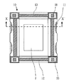
壁3の内面と蓋体4の下面とで囲まれる第2の空間部6内に水晶振動素子5を収容して蓋体4が載置されて気密封止されており、基板2の上面には水晶振動素子5の振動電極に接続される一対の搭載パッド等が、基板2の下面には後述する絶縁性基体10上の壁体13に接続される複数個の第2の接続電極部17がそれぞれ設けられ、これらのパッドや端子は基板2表面の配線パターンや基板内部に埋設されているビアホール等を介して、対応するもの同士、相互に電気的に接続されている。
2 ・・・基板
3 ・・・側壁
4 ・・・蓋体
5 ・・・水晶振動素子
6 ・・・第2の空間部
7 ・・・集積回路素子
8 ・・・導電性接合材
10・・・絶縁性基体
11・・・書込制御端子
12・・・半田層(金属層)
13・・・壁体
15・・・第1の空間部
17・・・第2の接続電極部
18・・・第1の接続電極部
19・・・電極端子
20・・・電極部
Claims (1)
- 水晶振動素子と、基板と、側壁と、蓋体とを備え、該側壁は、該基板の上面に該水晶振動素子を収容する第2の空間部を有するように設けられており、該蓋体は、該水晶振動素子を収容した該第2の空間部を気密封止するように該側壁の上面に載置固定されており、該基板の下面の四隅には第2の接続電極部が設けられている水晶振動子と、
集積回路素子と、
該集積回路素子を収容する凹形状の第1の空間部を表主面に有し、該第1の空間部を囲う壁体の上面における該第2の接続電極部と対向する位置に第1の接続電極部が設けられた絶縁性基体と
を備え、
該集積回路素子は、該絶縁性基体の該第1の空間部内に収容されており、
該水晶振動子が、該第2の接続電極部を該第1の接続電極部に接触させつつ該絶縁性基体の上に載置されており、
該第1の接続電極部と該第2の接続電極部とを機械的且つ電気的に接続した構成の水晶発振器において、
該第1の空間部を囲う該壁体の該上面には、該上面の全周にわたり半田層が形成されており、
該半田層は、該第1の接続電極部及び該第2の接続電極部と電気的に接続していない
ことを特徴とする水晶発振器。
Priority Applications (1)
| Application Number | Priority Date | Filing Date | Title |
|---|---|---|---|
| JP2006207965A JP4986529B2 (ja) | 2006-07-31 | 2006-07-31 | 水晶発振器 |
Applications Claiming Priority (1)
| Application Number | Priority Date | Filing Date | Title |
|---|---|---|---|
| JP2006207965A JP4986529B2 (ja) | 2006-07-31 | 2006-07-31 | 水晶発振器 |
Publications (3)
| Publication Number | Publication Date |
|---|---|
| JP2008035345A JP2008035345A (ja) | 2008-02-14 |
| JP2008035345A5 JP2008035345A5 (ja) | 2009-09-03 |
| JP4986529B2 true JP4986529B2 (ja) | 2012-07-25 |
Family
ID=39124279
Family Applications (1)
| Application Number | Title | Priority Date | Filing Date |
|---|---|---|---|
| JP2006207965A Expired - Fee Related JP4986529B2 (ja) | 2006-07-31 | 2006-07-31 | 水晶発振器 |
Country Status (1)
| Country | Link |
|---|---|
| JP (1) | JP4986529B2 (ja) |
Family Cites Families (6)
| Publication number | Priority date | Publication date | Assignee | Title |
|---|---|---|---|---|
| JP2974622B2 (ja) * | 1996-09-20 | 1999-11-10 | 松下電器産業株式会社 | 発振器 |
| JP3423255B2 (ja) * | 1999-06-04 | 2003-07-07 | 日本電波工業株式会社 | 表面実装水晶発振器 |
| JP2005065104A (ja) * | 2003-08-19 | 2005-03-10 | Murata Mfg Co Ltd | 表面実装型圧電振動子およびその製造方法 |
| JP4284142B2 (ja) * | 2003-09-26 | 2009-06-24 | 京セラ株式会社 | 圧電発振器 |
| JP4284143B2 (ja) * | 2003-09-26 | 2009-06-24 | 京セラ株式会社 | 圧電発振器 |
| JP4578231B2 (ja) * | 2004-11-25 | 2010-11-10 | 京セラ株式会社 | 圧電発振器及びその製造方法 |
-
2006
- 2006-07-31 JP JP2006207965A patent/JP4986529B2/ja not_active Expired - Fee Related
Also Published As
| Publication number | Publication date |
|---|---|
| JP2008035345A (ja) | 2008-02-14 |
Similar Documents
| Publication | Publication Date | Title |
|---|---|---|
| JP2008219206A (ja) | 圧電発振器 | |
| JP2008263564A (ja) | 温度補償型圧電発振器 | |
| JP4986529B2 (ja) | 水晶発振器 | |
| JP4724518B2 (ja) | 圧電発振器 | |
| JP4890914B2 (ja) | 水晶振動片の支持部構造 | |
| JP2007324933A (ja) | 圧電発振器とその製造方法 | |
| JP4376148B2 (ja) | 圧電発振器 | |
| JP5451266B2 (ja) | 電子デバイス | |
| JP2007103994A (ja) | 圧電発振器 | |
| JP4647339B2 (ja) | 水晶発振器及びその製造方法 | |
| JP2008061043A (ja) | 水晶発振器及びその製造方法 | |
| JP5101119B2 (ja) | 圧電発振器 | |
| JP4817929B2 (ja) | 水晶振動片の支持部構造 | |
| JP2008028860A (ja) | 圧電発振器 | |
| JP2008035175A (ja) | 圧電発振器 | |
| JP4328226B2 (ja) | 圧電発振器 | |
| JP4585847B2 (ja) | 水晶発振器及びその製造方法 | |
| JP2008141306A (ja) | 水晶発振器 | |
| JP4328225B2 (ja) | 温度補償型水晶発振器 | |
| JP2008035176A (ja) | 圧電発振器 | |
| JP2007067173A (ja) | 電子部品 | |
| JP2005244641A (ja) | 温度補償型水晶発振器 | |
| JP2007036808A (ja) | 圧電発振器 | |
| JP2007013721A (ja) | 圧電発振器 | |
| JP2006238252A (ja) | 水晶発振器及びその製造方法 |
Legal Events
| Date | Code | Title | Description |
|---|---|---|---|
| A521 | Request for written amendment filed |
Free format text: JAPANESE INTERMEDIATE CODE: A523 Effective date: 20090722 |
|
| A621 | Written request for application examination |
Free format text: JAPANESE INTERMEDIATE CODE: A621 Effective date: 20090722 |
|
| A977 | Report on retrieval |
Free format text: JAPANESE INTERMEDIATE CODE: A971007 Effective date: 20120116 |
|
| A131 | Notification of reasons for refusal |
Free format text: JAPANESE INTERMEDIATE CODE: A131 Effective date: 20120124 |
|
| A521 | Request for written amendment filed |
Free format text: JAPANESE INTERMEDIATE CODE: A523 Effective date: 20120326 |
|
| TRDD | Decision of grant or rejection written | ||
| A01 | Written decision to grant a patent or to grant a registration (utility model) |
Free format text: JAPANESE INTERMEDIATE CODE: A01 Effective date: 20120418 |
|
| A01 | Written decision to grant a patent or to grant a registration (utility model) |
Free format text: JAPANESE INTERMEDIATE CODE: A01 |
|
| A61 | First payment of annual fees (during grant procedure) |
Free format text: JAPANESE INTERMEDIATE CODE: A61 Effective date: 20120424 |
|
| R150 | Certificate of patent or registration of utility model |
Ref document number: 4986529 Country of ref document: JP Free format text: JAPANESE INTERMEDIATE CODE: R150 Free format text: JAPANESE INTERMEDIATE CODE: R150 |
|
| FPAY | Renewal fee payment (event date is renewal date of database) |
Free format text: PAYMENT UNTIL: 20150511 Year of fee payment: 3 |
|
| S531 | Written request for registration of change of domicile |
Free format text: JAPANESE INTERMEDIATE CODE: R313531 |
|
| R350 | Written notification of registration of transfer |
Free format text: JAPANESE INTERMEDIATE CODE: R350 |
|
| R250 | Receipt of annual fees |
Free format text: JAPANESE INTERMEDIATE CODE: R250 |
|
| R250 | Receipt of annual fees |
Free format text: JAPANESE INTERMEDIATE CODE: R250 |
|
| S111 | Request for change of ownership or part of ownership |
Free format text: JAPANESE INTERMEDIATE CODE: R313111 |
|
| R350 | Written notification of registration of transfer |
Free format text: JAPANESE INTERMEDIATE CODE: R350 |
|
| LAPS | Cancellation because of no payment of annual fees |