JP4957183B2 - Semiconductor device using backside high voltage integrated circuit - Google Patents
Semiconductor device using backside high voltage integrated circuit Download PDFInfo
- Publication number
- JP4957183B2 JP4957183B2 JP2006294207A JP2006294207A JP4957183B2 JP 4957183 B2 JP4957183 B2 JP 4957183B2 JP 2006294207 A JP2006294207 A JP 2006294207A JP 2006294207 A JP2006294207 A JP 2006294207A JP 4957183 B2 JP4957183 B2 JP 4957183B2
- Authority
- JP
- Japan
- Prior art keywords
- voltage
- switching element
- terminal
- semiconductor device
- input
- Prior art date
- Legal status (The legal status is an assumption and is not a legal conclusion. Google has not performed a legal analysis and makes no representation as to the accuracy of the status listed.)
- Active
Links
- 239000004065 semiconductor Substances 0.000 title claims description 86
- 239000004020 conductor Substances 0.000 claims description 24
- 239000000758 substrate Substances 0.000 claims description 21
- 239000003990 capacitor Substances 0.000 claims description 19
- 238000010586 diagram Methods 0.000 description 6
- 230000015556 catabolic process Effects 0.000 description 4
- 230000000694 effects Effects 0.000 description 3
- 230000001965 increasing effect Effects 0.000 description 2
- 230000001939 inductive effect Effects 0.000 description 2
- 230000007257 malfunction Effects 0.000 description 2
- 230000002457 bidirectional effect Effects 0.000 description 1
- 238000002485 combustion reaction Methods 0.000 description 1
- 230000008878 coupling Effects 0.000 description 1
- 238000010168 coupling process Methods 0.000 description 1
- 238000005859 coupling reaction Methods 0.000 description 1
- 230000020169 heat generation Effects 0.000 description 1
- 238000009413 insulation Methods 0.000 description 1
- 238000005549 size reduction Methods 0.000 description 1
Images


Classifications
-
- F—MECHANICAL ENGINEERING; LIGHTING; HEATING; WEAPONS; BLASTING
- F02—COMBUSTION ENGINES; HOT-GAS OR COMBUSTION-PRODUCT ENGINE PLANTS
- F02P—IGNITION, OTHER THAN COMPRESSION IGNITION, FOR INTERNAL-COMBUSTION ENGINES; TESTING OF IGNITION TIMING IN COMPRESSION-IGNITION ENGINES
- F02P3/00—Other installations
- F02P3/02—Other installations having inductive energy storage, e.g. arrangements of induction coils
- F02P3/04—Layout of circuits
- F02P3/0407—Opening or closing the primary coil circuit with electronic switching means
- F02P3/0435—Opening or closing the primary coil circuit with electronic switching means with semiconductor devices
-
- H—ELECTRICITY
- H01—ELECTRIC ELEMENTS
- H01L—SEMICONDUCTOR DEVICES NOT COVERED BY CLASS H10
- H01L2224/00—Indexing scheme for arrangements for connecting or disconnecting semiconductor or solid-state bodies and methods related thereto as covered by H01L24/00
- H01L2224/01—Means for bonding being attached to, or being formed on, the surface to be connected, e.g. chip-to-package, die-attach, "first-level" interconnects; Manufacturing methods related thereto
- H01L2224/42—Wire connectors; Manufacturing methods related thereto
- H01L2224/47—Structure, shape, material or disposition of the wire connectors after the connecting process
- H01L2224/48—Structure, shape, material or disposition of the wire connectors after the connecting process of an individual wire connector
- H01L2224/481—Disposition
- H01L2224/48135—Connecting between different semiconductor or solid-state bodies, i.e. chip-to-chip
- H01L2224/48137—Connecting between different semiconductor or solid-state bodies, i.e. chip-to-chip the bodies being arranged next to each other, e.g. on a common substrate
-
- H—ELECTRICITY
- H01—ELECTRIC ELEMENTS
- H01L—SEMICONDUCTOR DEVICES NOT COVERED BY CLASS H10
- H01L2224/00—Indexing scheme for arrangements for connecting or disconnecting semiconductor or solid-state bodies and methods related thereto as covered by H01L24/00
- H01L2224/01—Means for bonding being attached to, or being formed on, the surface to be connected, e.g. chip-to-package, die-attach, "first-level" interconnects; Manufacturing methods related thereto
- H01L2224/42—Wire connectors; Manufacturing methods related thereto
- H01L2224/47—Structure, shape, material or disposition of the wire connectors after the connecting process
- H01L2224/49—Structure, shape, material or disposition of the wire connectors after the connecting process of a plurality of wire connectors
- H01L2224/491—Disposition
- H01L2224/4912—Layout
- H01L2224/49175—Parallel arrangements
-
- H—ELECTRICITY
- H01—ELECTRIC ELEMENTS
- H01L—SEMICONDUCTOR DEVICES NOT COVERED BY CLASS H10
- H01L2924/00—Indexing scheme for arrangements or methods for connecting or disconnecting semiconductor or solid-state bodies as covered by H01L24/00
- H01L2924/10—Details of semiconductor or other solid state devices to be connected
- H01L2924/11—Device type
- H01L2924/13—Discrete devices, e.g. 3 terminal devices
- H01L2924/1301—Thyristor
-
- H—ELECTRICITY
- H01—ELECTRIC ELEMENTS
- H01L—SEMICONDUCTOR DEVICES NOT COVERED BY CLASS H10
- H01L2924/00—Indexing scheme for arrangements or methods for connecting or disconnecting semiconductor or solid-state bodies as covered by H01L24/00
- H01L2924/10—Details of semiconductor or other solid state devices to be connected
- H01L2924/11—Device type
- H01L2924/13—Discrete devices, e.g. 3 terminal devices
- H01L2924/1304—Transistor
- H01L2924/1305—Bipolar Junction Transistor [BJT]
- H01L2924/13055—Insulated gate bipolar transistor [IGBT]
-
- H—ELECTRICITY
- H01—ELECTRIC ELEMENTS
- H01L—SEMICONDUCTOR DEVICES NOT COVERED BY CLASS H10
- H01L2924/00—Indexing scheme for arrangements or methods for connecting or disconnecting semiconductor or solid-state bodies as covered by H01L24/00
- H01L2924/19—Details of hybrid assemblies other than the semiconductor or other solid state devices to be connected
- H01L2924/191—Disposition
- H01L2924/19101—Disposition of discrete passive components
- H01L2924/19107—Disposition of discrete passive components off-chip wires
Description
本発明は裏面高耐圧集積回路を用いた半導体装置に関し、特に、自動車のエンジン点火システム等に搭載される半導体装置に関するものである。 The present invention relates to a semiconductor device using a backside high voltage integrated circuit, and more particularly to a semiconductor device mounted on an engine ignition system of an automobile.
絶縁ゲートバイポーラトランジスタ(IGBT)に代表される電力半導体素子は、自動車のエンジン点火システムや、モータ等の制御に広く用いられている(例えば、特許文献1参照)。 A power semiconductor element typified by an insulated gate bipolar transistor (IGBT) is widely used for control of an automobile engine ignition system, a motor, and the like (see, for example, Patent Document 1).
自動車のエンジン点火システムに用いられる半導体装置の構成を図7に示す。半導体装置1は導電体2を用いて構成され、導電体2の上には、電力用半導体素子3及び絶縁基板5が離間して設けられている。絶縁基板5の上には、集積回路用半導体素子41、コンデンサや抵抗等の受動素子部6が設けられている。電力用半導体素子3と絶縁基板5は、配線8により接続されている。また、絶縁基板5には入出力用配線7aが接続され、導電体2には入出力用配線7bが接続されている。電力用半導体素子3としては、IGBTなどのスイッチング素子が用いられている。電力用半導体素子3は、配線8を介して集積回路用半導体素子41に接続されている。集積回路用半導体素子41は、電力用半導体素子3のオン・オフを制御するための制御回路を有している。
FIG. 7 shows a configuration of a semiconductor device used in an automobile engine ignition system. The
上記従来の半導体装置において、電力用半導体素子3を駆動させる際、導電体2上には高電位が発生する。そのため集積回路用半導体素子41を絶縁基板5の上に形成し、低い電圧で動作させるように構成されていた。そうすると、集積回路用半導体素子41の制御回路やパッケージを小型することが困難であるという問題があった。
In the conventional semiconductor device described above, when the
本発明は上記課題を解決するためになされたもので、その目的は、電力半導体素子と、これを制御するための集積回路用半導体素子とを有する半導体装置において、高機能化及び小型化を実現することである。 SUMMARY OF THE INVENTION The present invention has been made to solve the above-described problems, and an object of the present invention is to realize high functionality and miniaturization in a semiconductor device having a power semiconductor element and an integrated circuit semiconductor element for controlling the power semiconductor element. It is to be.
本発明に係る半導体装置は、入力側コイル及び出力側コイルを有し、前記入力側コイルに第1の電圧以上の電圧が印加されると前記出力側コイルに電流が流れる負荷コイルと、導電体と、前記導電体上で前記導電体と電気的に接続され、表面と裏面との間の耐圧が第1の耐圧であり、入力端子及び出力端子を有し、前記出力端子が前記負荷コイルの前記入力側コイルの一端に接続され、前記負荷コイルの前記入力側コイルに電圧を印加する第1のスイッチング素子と、前記導電体上で前記第1のスイッチング素子と離間して設けられ、表面と裏面との耐圧が前記第1の耐圧よりも大きい第2の耐圧である裏面高耐圧集積回路と、前記導電体上で前記第1のスイッチング素子及び前記裏面高耐圧集積回路と離間して設けられた絶縁基板と、前記絶縁基板に接続された入出力用の配線と、前記絶縁基板と前記第1のスイッチング素子とを接続する第1の配線と、前記絶縁基板と前記裏面高耐圧集積回路とを接続する第2の配線とを有し、前記裏面高耐圧集積回路は、前記第1のスイッチング素子の前記入力端子に接続され、前記第1のスイッチング素子のオン・オフを制御する制御回路と、前記負荷コイルの前記入力側コイルに接続されたコレクタと、接地されたエミッタと、前記負荷コイルの前記入力側コイルの電圧が出力されるベースとを有するサイリスタと、一方の端子が前記サイリスタの前記ベースに接続され、他方の端子が接地されたツェナーダイオードとを含み、前記第1のスイッチング素子がオンし、前記ツェナーダイオードの前記一方の端子に出力される電圧が前記第1の電圧よりも高い第2の電圧以上である場合、前記ツェナーダイオードの前記一方の端子から前記ツェナーダイオードの前記他方の端子に電流が流れることを特徴とする。本発明のその他の特徴については、以下において詳細に説明する。
A semiconductor device according to the present invention includes an input side coil and an output side coil, a load coil through which a current flows in the output side coil when a voltage equal to or higher than a first voltage is applied to the input side coil, and a conductor And the electrical conductor is electrically connected to the electrical conductor on the electrical conductor, the withstand voltage between the front surface and the back surface is the first withstand voltage, the input terminal and the output terminal, and the output terminal of the load coil A first switching element connected to one end of the input-side coil and applying a voltage to the input-side coil of the load coil; provided on the conductor and spaced apart from the first switching element; A back side high withstand voltage integrated circuit having a second withstand voltage greater than the first withstand voltage and a back side high withstand voltage integrated circuit provided on the conductor and spaced apart from the first switching element and the back side high withstand voltage integrated circuit. An insulating substrate; and An input / output wiring connected to the edge substrate, a first wiring connecting the insulating substrate and the first switching element, and a second connecting the insulating substrate and the back high voltage integrated circuit. A backside high withstand voltage integrated circuit connected to the input terminal of the first switching element, the control circuit for controlling on / off of the first switching element, and the load coil A thyristor having a collector connected to the input side coil, a grounded emitter, and a base from which the voltage of the input side coil of the load coil is output; one terminal connected to the base of the thyristor; A Zener diode having the other terminal grounded, the first switching element is turned on, and a voltage output to the one terminal of the Zener diode is For it is a high second voltage higher than the voltage, wherein said from one terminal of the Zener diode current flows to the other terminal of the Zener diode. Other features of the present invention are described in detail below.
本発明によれば、電力半導体素子と、これを制御するための集積回路用半導体素子とを有する半導体装置において、高機能化及び小型化を実現できる。 ADVANTAGE OF THE INVENTION According to this invention, in a semiconductor device which has a power semiconductor element and the semiconductor element for integrated circuits for controlling this, high functionality and size reduction are realizable.
以下、図面を参照しながら本発明の実施の形態について説明する。なお、各図において同一または相当する部分には同一符号を付して、その説明を簡略化ないし省略する。 Hereinafter, embodiments of the present invention will be described with reference to the drawings. In the drawings, the same or corresponding parts are denoted by the same reference numerals, and the description thereof is simplified or omitted.
実施の形態1.
本実施の形態1に係る半導体装置について説明する。図1に示すように、半導体装置1は、導電体2を用いて形成されている。導電体2の上には電力半導体素子としての第1のスイッチング素子3が設けられ、導電体2と電気的に接続されている。導電体2の上で、第1のスイッチング素子3と離間して、裏面高耐圧集積回路4が設けられている。
A semiconductor device according to the first embodiment will be described. As shown in FIG. 1, the
裏面高耐圧集積回路4の表面には、第1のスイッチング素子3のオン・オフを制御するための制御回路(ここでは図示しない)が設けられている。裏面高耐圧集積回路4の制御回路が形成されている領域(表面側)と裏面側との間の耐圧は、第1のスイッチング素子3の表面−裏面間の耐圧よりも大きくなるように構成されている。つまり、第1のスイッチング素子3の耐圧をV1、裏面高耐圧集積回路4の表面と裏面との間の耐圧をV2とすると、V1<V2の関係が成立している。このように半導体装置1は、裏面高耐圧集積回路4の表面−裏面間に、第1のスイッチング素子3の表面−裏面間の耐圧よりも大きい電圧が印加されても、裏面高耐圧集積回路4の絶縁性が維持されるように構成されている。
A control circuit (not shown here) for controlling on / off of the
導電体2の上で、第1のスイッチング素子3及び裏面高耐圧集積回路4と離間して、絶縁基板5が設けられている。絶縁基板5の上には、コンデンサ、抵抗素子等を含む受動素子部6が設けられている。絶縁基板5には、2本の入出力用配線7aが接続され、導電体2には1本の入出力用配線7bが接続されている。絶縁基板5と第1のスイッチング素子3は、2本の第1配線8aにより接続され、絶縁基板5と裏面高耐圧集積回路4は、2本の第2配線8bにより接続されている。
An
図1に示した半導体装置1では、同一の導電体上に、第1のスイッチング素子3と、このスイッチング素子のオン・オフを制御する制御回路を搭載した集積回路とを、導電性の接合部材を用いて搭載することができる。これにより、絶縁基板5のサイズを縮小化でき、上記制御回路の高集積化が可能となる。従って、半導体装置1を小型化し、パッケージ内への高密度実装を実現できる。さらに、同一の導電体上に電力用半導体素子と上記集積回路とを搭載したことにより、熱結合性が高く、過熱遮断の精度を向上させた半導体装置を得ることができる。
In the
次に、図1に示した半導体装置1の他の構成例について説明する。図2に示すように、絶縁基板5と第1のスイッチング素子3は、1本の第1配線8aにより接続されている。また、第1のスイッチング素子3と裏面高耐圧集積回路4は、1本の第3配線8cにより接続されている。その他については、図1と同様である。図2の構成によっても、図1の構成と同様の効果を得ることができる。
Next, another configuration example of the
以上説明したように、本実施の形態1に係る半導体装置によれば、電力半導体素子と、これを制御するための集積回路用半導体素子とを有する半導体装置において、高機能化及び小型化を実現することができる。 As described above, according to the semiconductor device according to the first embodiment, high performance and miniaturization are realized in a semiconductor device having a power semiconductor element and an integrated circuit semiconductor element for controlling the power semiconductor element. can do.
実施の形態2.
本実施の形態2に係る半導体装置について説明する。ここでは、実施の形態1と異なる点を中心に説明する。
A semiconductor device according to the second embodiment will be described. Here, the points different from the first embodiment will be mainly described.
自動車エンジンの内燃機関用イグニッションシステムであるエンジン点火用半導体装置では、電力半導体素子及びこれに接続された誘導負荷が搭載され、点火のタイミングをコンピュータにより制御している。ここで、制御信号がオンしたままであると、電力半導体素子が導通し続けるため、発熱により素子自体が破壊する可能性がある。これを防止するため、上述した半導体装置では、オン動作開始後から一定時間後に動作するタイマー回路を用いて、電力半導体素子を強制遮断させる機能が備えられている。しかし、上記強制遮断時には、誘導負荷に大きな起電力が発生するため、コンピュータが意図しないタイミングで点火が発生した場合には、誤点火により素子が破損する可能性もある。 In a semiconductor device for engine ignition which is an ignition system for an internal combustion engine of an automobile engine, a power semiconductor element and an inductive load connected thereto are mounted, and ignition timing is controlled by a computer. Here, if the control signal remains on, the power semiconductor element continues to conduct, and thus the element itself may be destroyed by heat generation. In order to prevent this, the above-described semiconductor device has a function of forcibly shutting off the power semiconductor element using a timer circuit that operates after a predetermined time from the start of the ON operation. However, at the time of the forced interruption, a large electromotive force is generated in the inductive load. Therefore, when ignition occurs at a timing that is not intended by the computer, there is a possibility that the element may be damaged due to erroneous ignition.
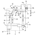
本実施の形態2に係る半導体装置は、実施の形態1で説明した裏面高耐圧集積回路に、サイリスタ及びツェナーダイオードを付加し、上記誤点火を抑制するようにしたものである。この半導体装置の回路図を図3に示す。 In the semiconductor device according to the second embodiment, a thyristor and a Zener diode are added to the back surface high voltage integrated circuit described in the first embodiment so as to suppress the false ignition. A circuit diagram of this semiconductor device is shown in FIG.
図3に示すように、半導体装置9は裏面高耐圧集積回路4と、これに接続された第1のスイッチング素子3を有している。第1のスイッチング素子3のコレクタ端子(出力端子3b)側には、負荷コイル10が接続されている。負荷コイル10は、エンジンの点火プラグ11及びバッテリ12に接続されている。負荷コイル10は、入力側コイル10a及び出力側コイル10bを有している。入力側コイル10aに所定の第1の電圧(V1)以上の電圧が印加されると、出力側コイル10bに電流が流れ、点火プラグ11が作動する。また、第1のスイッチング素子3のゲート−コレクタ間には、双方向ダイオード13が接続されている。このダイオードに所定値以上の電圧が印加されると電流が流れ、第1のスイッチング素子3を保護することができる。
As shown in FIG. 3, the
ここで、第1のスイッチング素子3は、入力端子3a及び出力端子3bを有している。出力端子3bは負荷コイル10の入力側コイル10aの下端(出力端子14)に接続されている。入力端子3aに所定の電圧が印加され、第1のスイッチング素子3がオン状態となると、負荷コイル10の入力側コイル10aには、高電圧が印加される。出力端子14には、裏面高耐圧集積回路4の裏面側に接続され、裏面高耐圧集積回路4の裏面側の電圧(裏面電圧)が出力される。
Here, the
裏面高耐圧集積回路4は制御回路15を有している。制御回路15は、第1のスイッチング素子3の入力端子3aに接続されている。そして、外部端子16から入力されるオン・オフの入力信号に応じて、第1のスイッチング素子3のオン・オフを制御する。
The back high voltage
さらに裏面高耐圧集積回路4は、PMOSトランジスタ17、抵抗18、NMOSトランジスタ19を有している。PMOSトランジスタ17は第1のスイッチング素子3の入力端子(ゲート)3aに接続されている。NMOSトランジスタ19のゲート及び制御回路15は、タイマー回路20に接続されている。タイマー回路20は、第1のスイッチング素子3がオン動作を開始した後に所定時間経過すると、第1のスイッチング素子3を強制的にオフさせる。
Further, the back high voltage
裏面高耐圧集積回路4は、pnpトランジスタ21及びnpnトランジスタ22により構成されるサイリスタ23を有している。サイリスタ23はコレクタ端子(C)、エミッタ端子(E)、ベース端子(B)を有している。コレクタ端子(C)は、出力端子14を介して負荷コイル10の入力側コイル10aに接続されている。エミッタ端子(E)は、抵抗26を介して接地されている。ベース端子(B)は、ツェナーダイオード24に接続されている。サイリスタ23がオンして電流が流れると、ベース端子(B)には、負荷コイル10の入力側コイル10aの電圧が出力される。
The back surface high voltage
上述したツェナーダイオード24の上端は、サイリスタ23のベース端子(B)に接続され、下端は、ツェナーダイオード25を介して接地されている。ツェナーダイオード24とツェナーダイオード25の接続点には、PMOSトランジスタ17及び抵抗18が接続されている。
The upper end of the
図3に示した半導体装置9では、第1のスイッチング素子3がオン状態である場合には、ツェナーダイオード24のカソード側(上端側)が出力端子14の電位とほぼ同電位となる。そして、ツェナーダイオード24のカソード側の電圧値が所定値(例えば、500V)以上である場合には、出力端子14からツェナーダイオード24のアノード側(下端側)に電流が流れる。ツェナーダイオード24のカソード側の電圧値が上記所定値未満である場合には、出力端子14からnpnトランジスタ22及び抵抗26を経由して電流が流れる。このようにして、出力端子14の電圧値を所定値以下に保つことができる。すなわち、第1のスイッチング素子3がオンしている間は、サイリスタ23により出力端子14の電圧が検出され、ツェナーダイオード24により、出力端子14の電圧が所定値以下に制御される。
In the
このように、第1のスイッチング素子3がオンし、ツェナーダイオード24の上方の端子に出力される電圧が、第1の電圧V1(≒負荷コイル10の出力側コイル10bに電流が流れる際に、入力側コイル10aに印加される電圧)よりも高い第2の電圧V2以上である場合、ツェナーダイオード24の上方の端子から下方の端子に電流が流れる。これにより、出力端子14の電圧は、上記第2の電圧V2以下に制御される。
Thus, when the
上記構成により、半導体装置9は、サイリスタ23を用いて裏面高耐圧集積回路4の裏面電圧を検出し、ツェナーダイオード24を用いて上記裏面電圧を所定値以下に制御し、負荷コイル10に大きな起電力が発生することを抑制できる。これにより、点火プラグ11での誤点火を防ぐことができる。従って、半導体装置を構成する面積を小さく保ったまま誤点火を抑制し、エンジンの保護及び半導体装置の自己保護を行うことが可能となる。
With the above configuration, the
本実施の形態2の半導体装置によれば、半導体装置を構成する面積を小さく保ったまま、誤点火を抑制し、エンジンの保護及び半導体装置の自己保護を行うことができる。 According to the semiconductor device of the second embodiment, misignition can be suppressed and the engine can be protected and the semiconductor device can be self-protected while keeping the area constituting the semiconductor device small.
実施の形態3.
本実施の形態3に係る半導体装置について説明する。ここでは、実施の形態2と異なる点を中心に説明する。
A semiconductor device according to the third embodiment will be described. Here, the points different from the second embodiment will be mainly described.
実施の形態2で示した半導体装置のスイッチング素子を駆動させる際には、コンピュータから制御回路を介してスイッチング素子にオン信号が伝達される。このとき、半導体装置には、スイッチング素子を駆動させるための電源を接続する必要があった。
When the switching element of the semiconductor device described in
本実施の形態3に係る半導体装置は、実施の形態2で説明した第1のスイッチング素子3がオフ状態である際に、このスイッチング素子の駆動に必要な電流を取り出してコンデンサに蓄えることにより、上記電源を不要としたものである。この半導体装置27の回路図を図4に示す。
In the semiconductor device according to the third embodiment, when the
図4に示すように、出力端子14は負荷コイル10に接続されている。負荷コイル10の入力側コイル10aの上方の端部は、バッテリ12に接続されている。
As shown in FIG. 4, the
裏面高耐圧集積回路4は、サイリスタ23と出力端子14との間に接続されたIGBT28を有している。IGBT28と出力端子14との間には、ツェナーダイオード29、抵抗30が接続されている。
The backside high voltage
IGBT28は、サイリスタ23を駆動させるための第2のスイッチング素子として機能する。IGBT28は、入力端子28aと、出力端子28bとを有している。入力端子28aは、負荷コイル10の入力側コイル10aを介して、バッテリ12に接続されている。出力端子28bは、サイリスタ23のコレクタ端子(C)に接続されている。
The
ここで、第1のスイッチング素子3がオンしている間は、出力端子14は高電位となる。そこで、抵抗30の抵抗値を大きくすることで、IGBT28のゲートに印加される電圧を低下させることができる。さらに、ツェナーダイオード29を設けたことにより、IGBT28のゲートに印加される電圧を所定値以下とし、IGBT28を保護することができる。
Here, while the
さらにnpnトランジスタ22のエミッタ端子(E)と抵抗26の接続点には、ダイオード31が接続されている。このダイオード31を介して、サイリスタ23のエミッタ端子(E)が、コンデンサ32の上端に接続されている。また、コンデンサ32の上端には、制御回路15も接続されている。コンデンサ32の下端は、接地されている。
Further, a
上記構成により、第1のスイッチング素子3がオフ状態の時は、出力端子14の電圧は、バッテリ12の電圧と等しくなる。そして、バッテリ12から供給される電圧により、IGBT28がオン状態となり、サイリスタ23がオンする。すると、バッテリ12から出力端子14、サイリスタ23、ダイオード31を経由して電流が流れ、コンデンサ32が充電される。
With the above configuration, when the
このように、第1のスイッチング素子3がオフ状態である場合には、バッテリ12から供給される電圧により、IGBT28がオンする。そして、バッテリ12からサイリスタ23を介してコンデンサ32に向かって電流が流れることにより、コンデンサ32が充電される。
Thus, when the
そして、制御回路15は、充電されたコンデンサ32を電源として、第1のスイッチング素子3のオン・オフの制御を行うことができる。その他の構成については、実施の形態2と同様である。
Then, the
上記構成とすることにより、第1のスイッチング素子3の駆動用電源が不要となる。これにより、半導体装置27を小型化することが可能となる。
With the above configuration, a driving power source for the
なお、図4に示した回路構成では、第1のスイッチング素子3がオフ状態にあるとき、バッテリ12からサージが入力されると、IGBT3のゲート電位が浮くことがある。そのため、IGBT3が駆動して誤動作する可能性も考えられる。しかし、半導体装置27は保護回路としてのみ機能するため、サージによる誤動作の恐れはなく、より安全に動作させることができる。
In the circuit configuration shown in FIG. 4, when a surge is input from the
本実施の形態3に係る半導体装置によれば、実施の形態1の効果に加えて、第1のスイッチング素子3を駆動するための電源が不要となるので、半導体装置を小型化することが可能となる。
According to the semiconductor device according to the third embodiment, in addition to the effects of the first embodiment, a power source for driving the
実施の形態4.
本実施の形態4に係る半導体装置について説明する。ここでは、実施の形態3と異なる点を中心に説明する。
A semiconductor device according to the fourth embodiment will be described. Here, the points different from the third embodiment will be mainly described.
本実施の形態4に係る半導体装置33の平面図を図5に示す。また、図5の半導体装置33を含む回路図を図6に示す。コンデンサ32及び制御回路15には、制御回路15に入力信号を与えるための無線モジュール34が接続されている。そして、無線モジュール34は、実施の形態3と同様にして充電されたコンデンサ32を電源として用いて、制御回路15に入力信号を与えることができる。その他の構成については、実施の形態3と同様である。
FIG. 5 shows a plan view of the
上記構成により、無線モジュールの駆動に必要な電流を、裏面高耐圧集積回路4の裏面電圧から取り出して、無線モジュール34に供給することができる。これにより、無線モジュール34を駆動させるための電源を設ける必要がない。また、無線モジュール34により、コンピュータからの入力信号を無線により伝達できるので、入力配線を無線化し、半導体装置を小型化することができる。さらに入力配線の無線化により、ノイズによる影響を受け難く、従来よりも信頼性の高い半導体装置を実現することができる。
With the above configuration, the current required for driving the wireless module can be extracted from the back surface voltage of the back surface high voltage
本実施の形態4に係る半導体装置によれば、実施の形態3の効果に加えて、半導体装置を小型化でき、かつ、信頼性を高くすることができる。 According to the semiconductor device according to the fourth embodiment, in addition to the effects of the third embodiment, the semiconductor device can be miniaturized and the reliability can be increased.
1 半導体装置、2 導電体、3 第1のスイッチング素子、4 裏面高耐圧集積回路、5 絶縁基板、6 受動素子部、7a、7b 入出力用配線、8a 第1配線、8b 第2配線、8c 第3配線、9 半導体装置、10 負荷コイル、14 出力端子、15 制御回路、20 タイマー回路、23 サイリスタ、24、25 ツェナーダイオード、27 半導体装置、28 IGBT(第2のスイッチング素子)、32 コンデンサ、33 半導体装置、34 無線モジュール。
DESCRIPTION OF
Claims (3)
導電体と、
前記導電体上で前記導電体と電気的に接続され、表面と裏面との間の耐圧が第1の耐圧であり、入力端子及び出力端子を有し、前記出力端子が前記負荷コイルの前記入力側コイルの一端に接続され、前記負荷コイルの前記入力側コイルに電圧を印加する第1のスイッチング素子と、
前記導電体上で前記第1のスイッチング素子と離間して設けられ、表面と裏面との耐圧が前記第1の耐圧よりも大きい第2の耐圧である裏面高耐圧集積回路と、
前記導電体上で前記第1のスイッチング素子及び前記裏面高耐圧集積回路と離間して設けられた絶縁基板と、
前記絶縁基板に接続された入出力用の配線と、
前記絶縁基板と前記第1のスイッチング素子とを接続する第1の配線と、
前記絶縁基板と前記裏面高耐圧集積回路とを接続する第2の配線とを有し、
前記裏面高耐圧集積回路は、
前記第1のスイッチング素子の前記入力端子に接続され、前記第1のスイッチング素子のオン・オフを制御する制御回路と、
前記負荷コイルの前記入力側コイルに接続されたコレクタと、接地されたエミッタと、前記負荷コイルの前記入力側コイルの電圧が出力されるベースとを有するサイリスタと、
一方の端子が前記サイリスタの前記ベースに接続され、他方の端子が接地されたツェナーダイオードとを含み、
前記第1のスイッチング素子がオンし、前記ツェナーダイオードの前記一方の端子に出力される電圧が前記第1の電圧よりも高い第2の電圧以上である場合、前記ツェナーダイオードの前記一方の端子から前記ツェナーダイオードの前記他方の端子に電流が流れることを特徴とする半導体装置。 A load coil having an input side coil and an output side coil, and a current flowing through the output side coil when a voltage equal to or higher than a first voltage is applied to the input side coil;
A conductor;
On the conductor, electrically connected to the conductor, a withstand voltage between the front surface and the back surface is a first withstand voltage, and has an input terminal and an output terminal, and the output terminal is the input of the load coil A first switching element connected to one end of the side coil and applying a voltage to the input side coil of the load coil;
A back side high withstand voltage integrated circuit provided on the conductor and spaced apart from the first switching element, and having a second withstand voltage greater than the first withstand voltage;
An insulating substrate provided on the conductor and spaced apart from the first switching element and the back surface high voltage integrated circuit;
Wiring for input / output connected to the insulating substrate;
A first wiring connecting the insulating substrate and the first switching element;
A second wiring connecting the insulating substrate and the back high-voltage integrated circuit;
The back high voltage integrated circuit is
A control circuit connected to the input terminal of the first switching element and controlling on / off of the first switching element;
A thyristor having a collector connected to the input side coil of the load coil, a grounded emitter, and a base from which the voltage of the input side coil of the load coil is output;
A Zener diode having one terminal connected to the base of the thyristor and the other terminal grounded,
When the first switching element is turned on and the voltage output to the one terminal of the Zener diode is equal to or higher than a second voltage higher than the first voltage, the one terminal of the Zener diode is A semiconductor device characterized in that a current flows through the other terminal of the Zener diode.
前記負荷コイルの前記入力側コイルを介して前記外部電源に接続された入力端子と、前記サイリスタの前記コレクタに接続された出力端子とを有する第2のスイッチング素子と、
一端が前記制御回路及び前記サイリスタの前記エミッタに接続され、他端が接地されたコンデンサとを更に含み、
前記第1のスイッチング素子がオフした場合に、前記外部電源から供給される電圧により前記第2のスイッチング素子がオンし、前記外部電源から前記サイリスタを介して前記コンデンサに電流が流れて前記コンデンサが充電され、
前記制御回路は、前記充電されたコンデンサを電源として前記第1のスイッチング素子のオン・オフを制御することを特徴とする請求項1に記載の半導体装置。 An external power source connected to the other end of the input side coil of the load coil;
A second switching element having an input terminal connected to the external power supply via the input side coil of the load coil, and an output terminal connected to the collector of the thyristor;
A capacitor having one end connected to the control circuit and the emitter of the thyristor and the other end grounded;
When the first switching element is turned off, the second switching element is turned on by a voltage supplied from the external power source, and a current flows from the external power source to the capacitor via the thyristor, so that the capacitor Charged
2. The semiconductor device according to claim 1, wherein the control circuit controls on / off of the first switching element using the charged capacitor as a power source.
前記無線モジュールは、前記コンデンサを電源として用いることを特徴とする請求項2に記載の半導体装置。 A wireless module for supplying an input signal to the control circuit is connected to the capacitor.
The semiconductor device according to claim 2, wherein the wireless module uses the capacitor as a power source.
Priority Applications (5)
| Application Number | Priority Date | Filing Date | Title |
|---|---|---|---|
| JP2006294207A JP4957183B2 (en) | 2006-10-30 | 2006-10-30 | Semiconductor device using backside high voltage integrated circuit |
| US11/673,756 US7787225B2 (en) | 2006-10-30 | 2007-02-12 | Semiconductor apparatus using back-side high-withstand-voltage integrated circuit |
| KR1020070098591A KR100924742B1 (en) | 2006-10-30 | 2007-10-01 | Semiconductor Apparatus Using Back-Side High-Withstand-Voltage Integrated Circuit |
| DE102007047727.0A DE102007047727B4 (en) | 2006-10-30 | 2007-10-05 | A semiconductor device using a high backside withstand voltage integrated circuit |
| CNB2007101622774A CN100550379C (en) | 2006-10-30 | 2007-10-08 | Use the semiconductor device of back-side high-withstand-voltage integrated circuit |
Applications Claiming Priority (1)
| Application Number | Priority Date | Filing Date | Title |
|---|---|---|---|
| JP2006294207A JP4957183B2 (en) | 2006-10-30 | 2006-10-30 | Semiconductor device using backside high voltage integrated circuit |
Publications (2)
| Publication Number | Publication Date |
|---|---|
| JP2008112828A JP2008112828A (en) | 2008-05-15 |
| JP4957183B2 true JP4957183B2 (en) | 2012-06-20 |
Family
ID=39265102
Family Applications (1)
| Application Number | Title | Priority Date | Filing Date |
|---|---|---|---|
| JP2006294207A Active JP4957183B2 (en) | 2006-10-30 | 2006-10-30 | Semiconductor device using backside high voltage integrated circuit |
Country Status (5)
| Country | Link |
|---|---|
| US (1) | US7787225B2 (en) |
| JP (1) | JP4957183B2 (en) |
| KR (1) | KR100924742B1 (en) |
| CN (1) | CN100550379C (en) |
| DE (1) | DE102007047727B4 (en) |
Cited By (1)
| Publication number | Priority date | Publication date | Assignee | Title |
|---|---|---|---|---|
| US10651113B2 (en) | 2016-05-31 | 2020-05-12 | Mitsubishi Electric Corporation | Semiconductor apparatus, ignition device for internal combustion engine, and internal combustion engine system |
Families Citing this family (6)
| Publication number | Priority date | Publication date | Assignee | Title |
|---|---|---|---|---|
| JP5157247B2 (en) * | 2006-10-30 | 2013-03-06 | 三菱電機株式会社 | Power semiconductor device |
| JP4781400B2 (en) * | 2008-06-20 | 2011-09-28 | 三菱電機株式会社 | Semiconductor device |
| JP5171979B2 (en) | 2011-04-08 | 2013-03-27 | 三菱電機株式会社 | Electronic control unit |
| JP5209090B2 (en) * | 2011-07-04 | 2013-06-12 | 三菱電機株式会社 | Semiconductor device |
| ITMI20131189A1 (en) * | 2013-07-16 | 2015-01-17 | Eldor Corp Spa | ELECTRONIC IGNITION SYSTEM FOR AN ENDOTHERMAL ENGINE |
| JP6275282B2 (en) * | 2015-01-13 | 2018-02-07 | 三菱電機株式会社 | Semiconductor device, manufacturing method thereof, and semiconductor module |
Family Cites Families (11)
| Publication number | Priority date | Publication date | Assignee | Title |
|---|---|---|---|---|
| JPH04185282A (en) * | 1990-11-20 | 1992-07-02 | Sanyo Electric Co Ltd | Hybrid integrated circuit device for switching power source |
| JPH0563139A (en) * | 1991-09-03 | 1993-03-12 | Fuji Electric Co Ltd | Semiconductor device |
| JP3381617B2 (en) * | 1998-04-03 | 2003-03-04 | 富士電機株式会社 | Switching power supply controlling semiconductor device and switching power supply having the same |
| JP3955396B2 (en) * | 1998-09-17 | 2007-08-08 | 株式会社ルネサステクノロジ | Semiconductor surge absorber |
| JP3707942B2 (en) * | 1998-12-17 | 2005-10-19 | 三菱電機株式会社 | Semiconductor device and semiconductor circuit using the same |
| JP2002116237A (en) * | 2000-10-10 | 2002-04-19 | Texas Instr Japan Ltd | Semiconductor integrated circuit |
| JP2002217416A (en) * | 2001-01-16 | 2002-08-02 | Hitachi Ltd | Semiconductor device |
| US6649978B2 (en) * | 2001-06-19 | 2003-11-18 | Koninklijke Philips Electronics N.V. | Semiconductor module having multiple semiconductor chips |
| JP4489485B2 (en) * | 2004-03-31 | 2010-06-23 | 株式会社ルネサステクノロジ | Semiconductor device |
| JP4565879B2 (en) * | 2004-04-19 | 2010-10-20 | ルネサスエレクトロニクス株式会社 | Semiconductor device |
| JP2006203470A (en) | 2005-01-19 | 2006-08-03 | Kyocera Corp | High-frequency module and wireless communication equipment |
-
2006
- 2006-10-30 JP JP2006294207A patent/JP4957183B2/en active Active
-
2007
- 2007-02-12 US US11/673,756 patent/US7787225B2/en active Active
- 2007-10-01 KR KR1020070098591A patent/KR100924742B1/en active IP Right Grant
- 2007-10-05 DE DE102007047727.0A patent/DE102007047727B4/en active Active
- 2007-10-08 CN CNB2007101622774A patent/CN100550379C/en active Active
Cited By (2)
| Publication number | Priority date | Publication date | Assignee | Title |
|---|---|---|---|---|
| US10651113B2 (en) | 2016-05-31 | 2020-05-12 | Mitsubishi Electric Corporation | Semiconductor apparatus, ignition device for internal combustion engine, and internal combustion engine system |
| DE112016006919B4 (en) | 2016-05-31 | 2021-09-16 | Mitsubishi Electric Corporation | Semiconductor device, ignition device for internal combustion engine and internal combustion engine system |
Also Published As
| Publication number | Publication date |
|---|---|
| US7787225B2 (en) | 2010-08-31 |
| CN100550379C (en) | 2009-10-14 |
| DE102007047727B4 (en) | 2014-05-28 |
| KR100924742B1 (en) | 2009-11-05 |
| US20080099838A1 (en) | 2008-05-01 |
| KR20080039217A (en) | 2008-05-07 |
| DE102007047727A1 (en) | 2008-05-08 |
| JP2008112828A (en) | 2008-05-15 |
| CN101174618A (en) | 2008-05-07 |
Similar Documents
| Publication | Publication Date | Title |
|---|---|---|
| JP4957183B2 (en) | Semiconductor device using backside high voltage integrated circuit | |
| CN105991118B (en) | Semiconductor device for igniter, igniter system, and ignition coil unit | |
| JP2010278188A (en) | Semiconductor integrated circuit device | |
| JP2006299988A (en) | Ignition device for internal combustion engine | |
| JP2009147995A (en) | Power supply control circuit | |
| EP0757442A2 (en) | Ignition coil driver module | |
| JP5095979B2 (en) | Overvoltage protection circuit | |
| JP6922563B2 (en) | Semiconductor device | |
| JP4052815B2 (en) | In-vehicle igniter and IGBT for in-vehicle igniter | |
| JP4360298B2 (en) | Ignition device for internal combustion engine | |
| KR20110139886A (en) | Gate drive circuit of inverter | |
| US6787881B2 (en) | Integrated power device with improved efficiency and reduced overall dimensions | |
| JP2001244463A (en) | Semiconductor device | |
| US8044652B2 (en) | Constant current control circuit | |
| JP4983571B2 (en) | Ignition device for internal combustion engine | |
| JP4590387B2 (en) | Glow plug drive | |
| JPH09209892A (en) | Ignition device for internal combustion engine | |
| JP2006166142A (en) | Overcurrent protective circuit and inverter provided with it | |
| JP2008160283A (en) | Load drive circuit and ignitor using the same | |
| JP2005191896A (en) | Semiconductor integrated circuit provided with output drive circuit | |
| JP6707874B2 (en) | Semiconductor device | |
| JP2011074905A (en) | Ignition igniter for internal combustion engine | |
| JP2022148509A (en) | Latch-up prevention circuit, semiconductor device, electronic device, and vehicle | |
| WO2017077814A1 (en) | Igniter | |
| JP2009281235A (en) | Power switch unit for ignition coil for internal combustion engine |
Legal Events
| Date | Code | Title | Description |
|---|---|---|---|
| A621 | Written request for application examination |
Free format text: JAPANESE INTERMEDIATE CODE: A621 Effective date: 20090212 |
|
| A977 | Report on retrieval |
Free format text: JAPANESE INTERMEDIATE CODE: A971007 Effective date: 20090428 |
|
| A131 | Notification of reasons for refusal |
Free format text: JAPANESE INTERMEDIATE CODE: A131 Effective date: 20110927 |
|
| A521 | Request for written amendment filed |
Free format text: JAPANESE INTERMEDIATE CODE: A523 Effective date: 20111101 |
|
| A131 | Notification of reasons for refusal |
Free format text: JAPANESE INTERMEDIATE CODE: A131 Effective date: 20111206 |
|
| A521 | Request for written amendment filed |
Free format text: JAPANESE INTERMEDIATE CODE: A523 Effective date: 20120201 |
|
| TRDD | Decision of grant or rejection written | ||
| A01 | Written decision to grant a patent or to grant a registration (utility model) |
Free format text: JAPANESE INTERMEDIATE CODE: A01 Effective date: 20120221 |
|
| A01 | Written decision to grant a patent or to grant a registration (utility model) |
Free format text: JAPANESE INTERMEDIATE CODE: A01 |
|
| A61 | First payment of annual fees (during grant procedure) |
Free format text: JAPANESE INTERMEDIATE CODE: A61 Effective date: 20120305 |
|
| FPAY | Renewal fee payment (event date is renewal date of database) |
Free format text: PAYMENT UNTIL: 20150330 Year of fee payment: 3 |
|
| R150 | Certificate of patent or registration of utility model |
Ref document number: 4957183 Country of ref document: JP Free format text: JAPANESE INTERMEDIATE CODE: R150 Free format text: JAPANESE INTERMEDIATE CODE: R150 |
|
| R250 | Receipt of annual fees |
Free format text: JAPANESE INTERMEDIATE CODE: R250 |
|
| R250 | Receipt of annual fees |
Free format text: JAPANESE INTERMEDIATE CODE: R250 |
|
| R250 | Receipt of annual fees |
Free format text: JAPANESE INTERMEDIATE CODE: R250 |
|
| R250 | Receipt of annual fees |
Free format text: JAPANESE INTERMEDIATE CODE: R250 |
|
| R250 | Receipt of annual fees |
Free format text: JAPANESE INTERMEDIATE CODE: R250 |
|
| R250 | Receipt of annual fees |
Free format text: JAPANESE INTERMEDIATE CODE: R250 |
|
| R250 | Receipt of annual fees |
Free format text: JAPANESE INTERMEDIATE CODE: R250 |
|
| R250 | Receipt of annual fees |
Free format text: JAPANESE INTERMEDIATE CODE: R250 |
|
| R250 | Receipt of annual fees |
Free format text: JAPANESE INTERMEDIATE CODE: R250 |