US8044652B2 - Constant current control circuit - Google Patents
Constant current control circuit Download PDFInfo
- Publication number
- US8044652B2 US8044652B2 US12/457,710 US45771009A US8044652B2 US 8044652 B2 US8044652 B2 US 8044652B2 US 45771009 A US45771009 A US 45771009A US 8044652 B2 US8044652 B2 US 8044652B2
- Authority
- US
- United States
- Prior art keywords
- constant current
- npn transistor
- transistor
- power supply
- type mos
- Prior art date
- Legal status (The legal status is an assumption and is not a legal conclusion. Google has not performed a legal analysis and makes no representation as to the accuracy of the status listed.)
- Expired - Fee Related, expires
Links
Images


Classifications
-
- G—PHYSICS
- G05—CONTROLLING; REGULATING
- G05F—SYSTEMS FOR REGULATING ELECTRIC OR MAGNETIC VARIABLES
- G05F1/00—Automatic systems in which deviations of an electric quantity from one or more predetermined values are detected at the output of the system and fed back to a device within the system to restore the detected quantity to its predetermined value or values, i.e. retroactive systems
- G05F1/10—Regulating voltage or current
- G05F1/46—Regulating voltage or current wherein the variable actually regulated by the final control device is DC
- G05F1/56—Regulating voltage or current wherein the variable actually regulated by the final control device is DC using semiconductor devices in series with the load as final control devices
Definitions
- the present invention relates to a constant current control circuit having a built-in shunt resistor for detecting a constant current flowing toward a load, more specifically relates to a squib drive circuit for use in a vehicle to control a constant current flowing toward a squib resistor for airbag inflation.
- a squib drive circuit that controls inflation of an in-vehicle airbag by controlling a constant current flowing toward a squib resistor.
- a squid drive circuit can be implemented in an airbag IC (integrated circuit).
- the shunt resistor is provided not on a squib resistor terminal side but a power supply terminal side in order to avoid an ESD (Electrostatic Discharge) input.
- a constant current control circuit is provided.
- the constant current control circuit is coupled with a first external load and a second external load.
- the constant current control circuit includes: a power supply terminal that a power supply voltage is applied to; a first semiconductor switching element that is connected with the power supply terminal and controls a first constant current, the first constant current flowing toward the first external load based on the power supply voltage; a second semiconductor switching element that is connected with the power supply terminal and controls a second constant current, the second constant current flowing toward the second external load based on the power supply voltage; a first output terminal that is connected with the first external load; a second output terminal that is connected with the second external load; a first shunt resistor that is connected between the first external load and the first semiconductor switching element, and detects the first constant current; a second shunt resistor that is connected between the second external load and the second semiconductor switching element, and detects the second constant current; a step up circuit that steps up the power supply voltage by a predetermined voltage; a first drive circuit that
- the first semiconductor switching element and the second semiconductor switching element are arranged in a same chip and located adjacent to each other in the chip.
- the first and second pads are located between the first semiconductor switching element and the second semiconductor switching element.
- the first and second pads are electrically connected with the power supply terminal, which is a single terminal common to the first and second pads.
- the first and second shunt resistors are located outward of a region containing the first and second semiconductor switching elements.
- the first and second shunt resistors can be located not between the first and second semiconductor switching elements but outward of the region containing the first and second semiconductor switching elements. Therefore, a temperature increase of the first and second shunt resistors due to a temperature increase of the first and second semiconductor switching elements can be suppressed.
- the first and second pads can be connected with the power supply terminal, which is the single and common terminal. Therefore, the number of terminals can be reduced.
- FIG. 1 is a block diagram illustrating a squib drive circuit according to a first exemplary embodiment
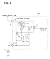
- FIG. 2 is a diagram illustrating a circuit configuration of the squib drive circuit illustrated in FIG. 1 ;
- FIG. 3 is a diagram illustrating a layout of the squib drive circuit illustrated in FIG. 1 ;
- FIG. 4 is a block diagram illustrating a squib drive circuit according to a second exemplary embodiment
- FIG. 5 is a diagram illustrating a circuit configuration of the squib drive circuit illustrated in FIG. 4 ;
- FIG. 6 is a diagram illustrating a layout of a squib drive circuit according to a third exemplary embodiment
- FIG. 7 is a diagram illustrating a circuit configuration of a squib drive circuit according to a fourth exemplary embodiment
- FIG. 8 is a diagram illustrating a layout of a squib drive circuit according to a fifth exemplary embodiment
- FIG. 9 is a cross sectional diagram taken along line IX-IX in FIG. 8 ;
- FIG. 10 is a block diagram illustrating a squib drive circuit according to a first comparison example
- FIG. 11 is a block diagram illustrating a squib drive circuit according to a second comparison example
- FIG. 12 is a diagram illustrating a circuit configuration of the squib drive circuit illustrated in FIG. 10 ;
- FIG. 13 is a diagram illustrating a circuit configuration of the squib drive circuit illustrated in FIG. 11 ;
- FIG. 14 is a diagram illustrating a layout of the squib drive circuit illustrated in FIGS. 10 , 11 .
- a constant current control circuit is illustrated by using a squib drive circuit for use in a vehicle to control airbag inflation.
- FIG. 10 illustrates a squib drive circuit 100 that employs a Pch type MOS transistor as a semiconductor switching element functioning as a high-side switch.
- FIG. 11 illustrates a squib drive circuit 100 that employs an Nch type MOS transistor as a high-side switch.
- FIG. 12 illustrates a specific circuit configuration of the squid drive circuit shown in FIG. 10 .
- FIG. 13 illustrates a specific circuit configuration of the squib drive circuit shown in FIG. 11 . It should be noted that, among multiple circuit systems of the squib drive circuit shown in FIGS.
- FIGS. 12 , 13 only a circuit system for driving a squib resistors is shown in FIGS. 12 , 13 .
- Another circuit system of the squib drive circuit 100 may have a circuit configuration similar to that shown in FIGS. 12 , 13 .
- the squib drive circuit 100 shown in each of FIGS. 10 and 11 performs constant current control by converting of currents flowing toward squib resistors 1 , 2 into voltages by using shunt resistors 3 , 4 , transferring the voltages to the first and second drive circuits 5 , 6 , and feedback-controlling gate voltages of the Pch type MOS transistors.
- the squib resistors 1 , 2 respectively acts as first and second external load and correspond to airbags, which can be equipped in various parts of the vehicle.
- the squib resistors 1 , 2 can cause explosion for the airbags to inflate.
- the squib drive circuit 100 shown in FIG. 10 has the following configuration.
- the Pch type MOS transistors 7 a , 8 a function as high-side switches.
- the shunt resistors 3 , 4 are connected on a high side more than the Pch type MOS transistors 7 a , 8 a .
- a power supply voltage VB is applied to the shunt resistors 3 , 4 , a first drive circuit 5 , and a second drive circuit 6 via power supply terminals 27 , 28 .
- the Pch type MOS transistors 7 a , 8 a are respectively connected with the squib resistors 1 , 2 via output terminals 11 , 12 .
- bases of two PNP transistors 13 b , 14 b are connected with each other so as to establish current-mirror connection whose current mirror ratio is set to 1:n.
- An emitter of one PNP transistor 13 b is connected with a low-side of the shunt resistor.
- An emitter of the other PNP transistor 14 b is connected with a high-side of the shunt resistor.
- Collectors of the PNP transistors 13 b , 14 b are respectively connected with constant current circuits 15 , 16 .
- a connection point between the collector of the PNP transistor 14 b and the constant current circuit 16 is connected with the gate of the Pch type MOS transistor 7 a .
- the power supply voltage VB is applied to the gate of the Pch type MOS transistor 7 a.
- the drive transistor 17 In a normal state of the above-configured squib drive circuit 100 , the drive transistor 17 is in ON, and thus, the Pch type MOS transistors 7 a , 8 a are in OFF, and currents do not flow toward the squib resistors 1 , 2 .
- the drive transistor 17 In timing for airbag to inflate following vehicle collision detection or the like, the drive transistor 17 is switched on and the gate of the Pch type MOS transistor 7 a is subjected to a voltage lower than “the power supply voltage VB minus a threshold voltage VT”. Thereby, the Pch type MOS transistor 7 a is switched on, and the current is allowed to flow through the squib resistor 1 .
- the current flowing toward the squib resistor 1 is converted into a voltage by the shunt resistor 3 .
- the gate electric potential of the Pch type MOS transistor 7 a is controlled in accordance with the change, and the source-drain current of the Pch type MOS transistor 7 a is controlled.
- the constant current control is performed so that the current flowing toward the squib resistor 1 is maintained constant.
- a squib drive circuit 100 illustrated in FIG. 11 has the following configuration. Nch type MOS transistors are used as high-side switches. The shunt resistors 3 , 4 are connected on a high side more than the Nch type MOS transistors 7 b , 8 b . The power supply voltage VB is applied to the shunt resistors 3 , 4 via the power supply terminals 27 , 28 , respectively. The Nch type MOS transistors 7 b , 8 b are respectively connected with the squib resistors 1 , 2 via the output terminals 11 , 12 . The squib drive circuit 100 shown in FIG. 11 includes a step up circuit 10 , differently from the squib drive circuit 100 shown in FIG.
- the step up circuit 10 steps up the power supply voltage VB and applies the stepped up power supply voltage VB to the first and second drive circuits 5 , 6 , in order for the squib drive circuit 100 to normally operate even when electric potentials of the output terminals change to as high as the power supply voltage VB. Because of the above-described configuration, by respectively inputting voltage drops across the shunt resistors 3 , 4 to the first and second drive circuits 5 , 6 , the gate potentials of the Nch type MOS transistors 7 b , 8 b are controlled, and the currents flowing toward the squib resistors 1 , 2 are controlled.
- bases of two PNP transistors 13 b , 14 b are connected with each other so as to establish current-mirror connection whose current mirror ratio is set to 1:n.
- An emitter of one PNP transistor 13 b is connected with a low-side of the shunt resistor.
- An emitter of the other PNP transistor 14 b is connected with a high-side of the shunt resistor.
- a collector and a base of the PNP transistor 13 b are connected with the constant current circuit 15
- a collector of the PNP transistor 14 b is connected with a collector and a base of an NPN transistor 29 .
- a base of the NPN transistor 29 and that of the NPN transistor 30 are connected with each other.
- a collector of the NPN transistor 30 is connected with a constant current circuit 16 , to which an electric potential that is stepped up from the power supply voltage VB by the step up circuit is applied.
- a connection point between the collector of the NPN transistor 30 and the constant current circuit. 16 is connected with the gate of the Nch type MOS transistor 7 b .
- the electric potential stepped up from the power supply voltage VB is applied to the gate of the Nch type MOS transistor 7 b.
- the drive transistor 17 In a normal state of the above configured squib drive circuit 100 , the drive transistor 17 is in ON, and thus, the Nch type MOS transistor 7 b is in OFF, and a current does not flow toward the squib resistor 1 .
- the drive transistor 17 In timing for airbags to inflate following vehicle collision detection or the like, the drive transistor 17 is switched off, and the gate of the Nch type MOS transistors 7 b is subjected to a voltage greater than or equal to a threshold voltage VT. Thereby, the Nch type MOS transistor 7 b is switched on, and the current is allowed to flow toward the squib resistor 1 . Then, the current flowing toward the squib resistor 1 is converted into a voltage by the shunt resistor 3 .
- the Pch type MOS transistors 7 a , 8 a or the Nch type MOS transistor 7 b , 8 b are connected with the power supply terminals 27 , 28 via the shunt resistors 3 , 4 , respectively. Because of the above configurations, the squib drive circuits 100 have the following layout. As shown in FIG. 14 , a group of elements including the shunt resistors 3 , 4 and pads 18 , 19 is located between the Pch type MOS transistors 7 a and 8 a or between the Nch type MOS transistors 7 b and 8 b .
- the shunt resistors 3 , 4 are respectively connected with the power supply terminals 27 , 28 via the pads 18 , 19 .
- the shunt resistors 3 , 4 are illustrated as resistors.
- the shunt resistors 3 , 4 may be merely wiring resistances provided by parts of a wiring pattern.
- a layout of the first and second drive circuits 5 , 6 which is not shown in FIG. 14 , may be such that the first and second drive circuits 5 , 6 are located adjacent to the Pch type MOS transistor 7 a , 8 a or the Nch type MOS transistors 7 b , 8 b of a corresponding circuit system.
- an semiconductor switching element such as a Pch type MOS transistor 7 a , 8 a and an Nch type MOS transistor 7 b , 8 b
- a heat value per unit area can be increasing accordingly.
- the shunt resistors 3 , 4 in the above-described layout are easy to receive heat, the shunt resistors 3 , 4 increase in temperature, and the temperature increase may results in the accuracy reduction of constant current control, the fracture life reduction of the shunt resistors 3 , 4 , the fusing of the shunt resistors 3 , 4 or the like.
- the layout shown in FIG. 14 may be modified in the following way: the shunt resistors 3 , 4 are placed outward of a region containing the Pch type MOS transistors 7 a , 8 a or the Nch type MOS transistors 7 b , 8 b .
- the shunt resistors 3 , 4 can be placed so as to be distant from the Pch type MOS transistors 7 a , 8 a or the Nch type MOS transistors 7 b , 8 b . It is thus possible to suppress a temperature increase of the shunt resistors 3 , 4 .
- the pads 18 and 19 become distant from each other, and the power supply terminals 27 , 28 connected with the pads 18 , 19 are difficult to be integrated in one common terminal. The number of terminals cannot be reduced.
- the number of squib resistors is not limited to two.
- the number of squib resistors may be more than 2. In such a case, at least two circuit systems may share a common power supply terminal.
- FIG. 1 is a block diagram illustrating a squib drive circuit 100 according to a first exemplary embodiment.
- a Pch type MOS transistor 7 a and another Pch type MOS transistor 8 a are respectively used as a first semiconductor output switching element and a second semiconductor output switching element that function as high-side switches.
- FIG. 2 illustrates a specific circuit configuration of the squib drive circuit 100 illustrated in FIG. 1 . It should be noted that, among multiple circuit systems of the squib drive circuit 100 , only a circuit system for driving a squib resistor 1 is shown in FIG. 2 . Another circuit system of the squib drive circuit 100 may have a circuit configuration similar to that shown in FIG. 2 .
- FIG. 3 illustrates a layout of the squib drive circuit 100 illustrated in FIG. 1 . Referring to FIG. 1 to 3 , explanation is given below on the squib drive circuit 100 .
- the squib drive circuit 100 performs constant current control by converting currents flowing toward squib resistors 1 , 2 into voltages by using shunt resistors 3 , 4 , transferring the voltages to first and second drive circuits 5 , 6 , and feedback-controlling gate voltages of the Pch type MOS transistors.
- the squib resistors 1 , 2 may be explosive devices for airbags of a vehicle to inflate, and may be placed as corresponding to the airbags equipped in various parts of the vehicle.
- the squib resistors 1 , 2 can act as firsthand second external load, respectively.
- the Pch type MOS transistors 7 a , 8 a are used as first and second semiconductor switching elements that function as high-side switches.
- the shunt resistors 3 , 4 are arranged on a low side more than the Pch type MOS transistors 7 a , 8 a .
- Drains of the Pch type MOS transistors 7 a , 8 a are connected with one power supply terminal 9 , which is common to the Pch type MOS transistors 7 a , 8 a .
- a step up circuit 10 steps up a power source Voltage VB, and an electric potential stepped up by the step up circuit 10 is applied to the first and second drive circuits 5 , 6 .
- the shunt resistors 3 , 4 are respectively connected with the squib resistors 1 , 2 via output terminals 11 , 12 . Because of the above configuration, voltage drops across the shunt resistors 3 , 4 are respectively inputted to the first and second drive circuits 5 , 6 , and accordingly, the gate potentials of the Pch type MOS transistors 7 a , 8 a are controlled, and the currents flowing toward the squib resistors 1 , 2 are controlled.
- bases of two NPN transistors 13 a , 14 a are connected with each other so as to establish a current-mirror connection whose current mirror ratio is set to 1:n.
- An emitter of one NPN transistors 13 a is connected with a low-side of the shunt resistor 3 .
- An emitter of the other NPN transistor 14 a is connected with a high-side of the shunt resistor 3 .
- Collectors of the NPN transistors 13 a , 14 a are respectively connected with the constant current circuits 15 , 16 .
- Each of the constant current circuits 15 , 16 creates a constant current based on the voltage that is stepped up from the power supply voltage VB by the step up circuit 10 .
- a connection point between the collector of the NPN transistor 14 a and the constant current circuit 16 is connected with the gate of the Pch type MOS transistor 7 a .
- the power supply voltage VB is applied to the gate of the Pch type MOS transistor 7 a .
- the squib drive circuit 100 employs a Pch type MOS transistor as the drive transistor 17 .
- the drive transistor 17 In a normal state of the above-configured squib drive circuit 100 , the drive transistor 17 is in ON, and thus, the Pch type MOS transistors 7 a , 8 a are in OFF, and currents do not flow toward the squib resistors 1 , 2 .
- the drive transistor 17 In timing of airbag inflation following vehicle collision detection or the like, the drive transistor 17 is switched on and the gates of the Pch type MOS transistors 7 a , 8 a are subjected to voltages lower than “the power supply voltage VB minus a threshold voltage VT”. Thereby, the Pch type MOS transistors 7 a , 8 a are switched on, and currents are allowed to flow through the squib resistors 1 , 2 .
- the step up circuit 10 steps up the power supply voltage VB by a predetermined voltage and creates the stepped up electric potential, even if an electric potential of the output terminal 11 or 12 becomes as high as the power supply voltage VB, the constant current circuits 15 , 16 can create constant currents supplied to the NPN transistors 13 a , 14 a . Then, the currents flowing toward the squib resistors 1 , 2 are converted into voltages by the shunt resistors 3 , 4 .
- the gate electric potentials of the Pch type MOS transistors 7 a , 8 a are controlled in accordance with the change, and the source-drain currents of the Pch type MOS transistors 7 a , 8 a are controlled. Accordingly, the currents flowing through the NPN transistors 13 a , 14 a are changed, and the constant currents created by the constant current circuits 15 , 16 are changed so that the change of the currents flowing through the NPN transistors 13 a , 14 a are adjusted and compensated.
- the constant current control is performed so that the currents flowing toward the squib resistors 1 , 2 become constant.
- the shunt resistors 3 , 4 are respectively connected with the output terminals 11 , 12 .
- the power supply terminal 9 of the squib drive circuit 100 is one common terminal. Further, the shunt resistors 3 , 4 are connected not between the power supply terminal 9 and the Pch type MOS transistors 7 a , 8 a but between the Pch type MOS transistors 7 a , 8 a and the output terminals 11 , 12 .
- the squib drive circuit 100 of the present embodiment has the following layout. As shown in FIG. 3 , the Pch type MOS transistor 7 a of one circuit system and the Pch type MOS transistor 8 a of another circuit system are placed adjacent to each other in the same chip. Pads 18 , 19 , to which the power supply voltage VB are applied, are placed between the Pch type MOS transistors 7 a and 8 a . Pads 20 , 21 , which are connected with the shunt resistors 3 , 4 , are placed outward of a region containing the Pch type MOS transistors 7 a , 8 a . The pads 18 , 19 are electrically connected with the common one power supply terminal 9 by using a wiring 22 such as wire bonding and the like. The pads 20 , 21 are respectively and electrically connected with the output terminals 11 , 12 by using a wiring 23 such wire bonding and the like.
- the shunt resistor 3 or 4 of another circuit system is distant from the Pch type MOS transistors 7 a , 8 a that is driven, and thus, it is possible to further suppress a temperature increase of the shunt resistor 3 or 4 .
- the power supply terminal 9 is provided as one common terminal, it is possible to reduce the number of terminals.
- the emitter of the NPN transistor 13 a , 14 a may receive the ESD surge when electrostatic discharge (ESD) surge is inputted via the output terminal 11 , 12 or the like. Since an emitter of an NPN transistor is typically susceptible to electrostatic breakdown, a concern arises about Zener breakdown between the emitter and the base. In view of the above concern, according to the present embodiment, when the NPN transistors 13 a and 14 a are integrated in one chip, elements may be formed and separated with trench isolation structure but not with junction separation. By using the trench isolation, it is possible to minimize malfunction when the ESD surge is inputted.
- a second exemplary embodiment is described below.
- the second exemplary embodiment is a modification of the first exemplary embodiment.
- Nch type MOS transistors 7 b , 8 b drive the squib drive circuit 100 for instance.
- FIG. 4 is a block diagram illustrating a squib drive circuit 100 according to the present embodiment.
- the Nch type MOS transistors 7 b , 8 b are respectively used as first and second semiconductor output switching elements, which function as high-side switches.
- FIG. 5 illustrates one specific circuit configuration of the squib drive circuit illustrated in FIG. 4 . It should be noted that, among multiple circuit systems of the squib drive circuit 100 , only a circuit system for driving a squib resistor 1 is shown in FIG. 4 . Another circuit system of the squib drive circuit 100 may have a circuit configuration similar to that shown in FIG. 4 . A layout shown in FIG. 3 can be used as a layout of the squib drive circuit 100 illustrated in FIG. 4 . Referring to FIGS. 4 and 5 , explanation is given below on the squib drive circuit 100 of the present embodiment.
- the Nch type MOS transistors 7 b , 8 b are used in place of the Pch type MOS transistors 7 a , 8 a .
- the drive transistor 17 is also an Nch type MOS transistor.
- the drive transistor 17 is connected between the gate of the Nch type MOS transistor 7 b , 8 b and GND. By controlling the gate electric potential of the drive transistor 17 , the Nch type MOS transistor 7 b , 8 b are driven.
- the NPN transistors 13 a , 14 a are current-mirror-connected with each other.
- the emitter of the NPN transistor 13 a is connected with a high side of the shunt resistor 3 , 4
- the emitter of the NPN transistor 14 a is connected with a low side of the shunt resistor 3 , 4 .
- the drive transistor 17 In a normal state of the above configured squib drive circuit 100 , the drive transistor 17 is in ON, and thus, the Nch type MOS transistors 7 b , 8 b are in OFF, and currents do not flow though the squib resistors 1 , 2 .
- the drive transistor 17 In timing of airbag inflation following vehicle collision detection or the like, the drive transistor 17 is switched off, and voltages greater than or equal to a threshold voltage VT are applied to the gates of the Nch type MOS transistors 7 b , 8 b . Thereby, the Nch type MOS transistor 7 b , 8 b are switched on, and the currents are allowed to flow through the squib resistors 1 , 2 .
- the step up circuit 10 steps up the power supply voltage VB by a predetermined voltage and creates the stepped up electric potential, even if an electric potential of the output terminal 11 or 12 becomes as high as the power supply voltage VB, the constant current circuits 15 , 16 can create constant currents to be supplied to the NPN transistors 13 a , 14 a . Then, the currents flowing toward the squib resistors 1 , 2 are converted into voltages by the shunt resistors 3 , 4 .
- the shunt resistors 3 , 4 are respectively connected with the output terminals 11 , 12 .
- the power supply terminal 9 is one common terminal. Further, the shunt resistors 3 , 4 are connected not between the power supply terminal 9 and the Pch type MOS transistors 7 b , 8 b but between the Pch type MOS transistors 7 b , 8 b and the output terminals 11 , 12 .
- the layout of the squib drive circuit 100 of the present embodiment can be generally similar to the layout shown in FIG. 3 . Accordingly, the squib drive circuit 100 of the present embodiment can have the same advantages as that of the first exemplary embodiment.
- a third exemplary embodiment is described below.
- the third exemplary embodiment is a modification of the first exemplary embodiment or second exemplary embodiment.
- the pads 18 , 19 connected to the power supply terminal 9 are integrated into a common pad.
- a circuit configuration of the squib drive circuit 100 of the present embodiment can be the same as that of the first exemplary embodiment or the second exemplary embodiment. A difference lies in layout.
- FIG. 6 illustrates a layout of a squib drive circuit 100 according to the present embodiment.
- the Pch type MOS transistors 7 a , 8 a or the Nch type MOS transistors 7 b , 8 b are electrically connected with the power supply terminal via a pad 24 .
- the pad 24 is arranged between the Pch type MOS transistors 7 a and 8 a or between the Nch type MOS transistors 7 b and 8 b while being aligned.
- a pad connected with the Pch type MOS transistor 7 a and that connected with the P type MOS transistor 8 a are integrated into a common pad, or, a pad connected with the Nch type MOS transistor 7 b and that connected with the N type MOS transistor 8 b are integrated into a common pad.
- the common pad 24 it becomes possible to downsize an apparatus.
- a fourth exemplary embodiment is described below.
- the fourth exemplary embodiment is a modification of the first exemplary embodiment.
- a squib drive circuit 100 of the present embodiment further includes a limiting resistor.
- FIG. 7 is a block diagram illustrating a squib drive circuit 100 according to the present embodiment.
- a limiting resistor 25 is connected between the NPN transistor 13 a and the shunt resistor 3 , 4
- a limiting resistor 26 is connected between the NPN transistor 14 a and the shunt resistor 3 , 4 . Because of the presence of the limiting resistors 25 , 26 , if ESD surge is inputted via the output terminals 11 , 12 or the like, a current caused by the ESD surge can be reduced by the limiting resistors 25 , 26 . Thus, it is possible to minimize malfunction when the ESD surge is inputted.
- the squib drive circuit 100 of the present embodiment may further include a clamp circuit that clamps an upper limit of voltage inputted from the output terminal 11 , 12 .
- each output terminal 11 , 12 is connected with a MOS transistor via a diode, and a Zener diode is connected between a source and a base of the MOS transistor.
- FIG. 8 illustrates a layout of a squib drive circuit according to the present embodiment.
- FIG. 9 illustrates a cross section taken along line IX-IX in FIG. 8 .
- trench isolation structures 31 , 32 are formed so as to surround the Pch type MOS transistors 7 a , 8 a , respectively.
- a p + type source region 48 and a p + type drain region 49 are formed in a surface portion of the active layer 43 so as to be spaced apart from each other. A part of the surface portion between the p + type source region 48 and the p + type drain region 49 functions as a channel region.
- a gate electrode 51 is formed above a surface of the channel region while a gate insulator film 50 is interposed between the gate electrode 51 and the surface of the channel region.
- An element region of the Pch type MOS transistor 7 a is formed in the above arrangement. The element region is surrounded by the trench isolation structure 31 . It should be noted that, although a cross section of the trench isolation structure 32 is not shown in FIG. 9 , the trench isolation structure 32 and the trench isolation structure 31 may have generally identical structure.
- the shunt resistor 3 is provided as a wiring resistance of a wiring.
- the NPN transistor 13 a , 14 a is located below the wiring.
- the Pch type MOS transistor 7 a , 8 a has the following structure.
- a source electrode 53 is electrically connected with the p + type source region 48 though a contact hole formed in the interlayer insulation film 52 .
- a drain electrode 54 is electrically connected with a p + type drain region 49 .
- a wiring pattern 56 is formed on an interlayer insulating film 55 .
- the wiring pattern 56 includes a source wiring part 56 a electrically connected with the source electrode 53 and a drain wiring part 56 b electrically connected with the drain electrode 54 .
- the wiring pattern 56 further includes a wiring resistance part 56 c and a connection part 56 d .
- the wiring resistance part 56 c acts as the shunt resistor 3 and is located adjacent to the source wiring part 56 a and the drain wiring part 56 b .
- the connection part 56 d connects the drain wiring part 56 b and the pad 18 .
- the NPN transistors 13 a , 14 a are located below the shunt resistor 3 , which is provided as the wiring resistance part 56 c.
- FIG. 9 illustrates the p type base region 57 and the p type emitter region 58
- an n + type collector region etc. is formed in a part of the NPN transistor 7 a that is located outside of the page space of FIG. 9 in a direction perpendicular to the page space.
- the circuit system that has the shunt resistor 4 is not shown in FIG. 9
- an NPN transistor of the un-shown circuit system is also located below the shunt resistor 4 .
- the NPN transistors 13 a and 14 a are located adjacent to each other, and an alignment direction of the NPN transistors 13 a and 14 a is parallel to the Pch type MOS transistor 7 a , which can become a relatively large heat source.
- the NPN transistors 13 a and 14 a are equal to each other in distance from the Pch type MOS transistor 7 a.
- the trench isolation structures 31 , 32 respectively surround the Pch type MOS transistors 7 a , 8 a as seen above, it is possible to suppress conduction of the heat generated by each Pch type MOS transistor 7 a , 8 a to its surrounding region including a region of another circuit system, compared to the use of PN isolation or the like. Further, it is possible to suppress conduction of heat in the surrounding region to the Pch type MOS transistor 7 a , 8 a.
- the Pch type MOS transistor 7 a , 8 a can become a major heat source. If the heat were conducted to the surrounding region, the heat would cause an error; for example, the heat could influence operation of the NPN transistor 13 a , 14 a in some cases. Further, if the Pch type MOS transistor 7 a , 8 a were subjected to the heat from another circuit system, the heat would influence operation of the Pch type MOS transistor 7 a , 8 a in some cases. In view of the above-described possibility, in the present embodiment, the Pch type MOS transistor 7 a , 8 a are surrounded by the trench isolation structures 31 , 32 , and is thermally isolated from another region.
- the use of the trench isolation structure 31 , 32 reduces a leak current more efficiently than the use of the PN isolation. Further, the trench isolation structure 31 , 32 can be placed closer to the Pch type MOS transistor 7 a , 8 a acting as the heat source compared to the PN isolation, and thus, it is possible reduce an non-active area.
- the shunt resistor 3 and the NPN transistors 13 a and 14 a are equal to each other in distance from a heat generation source of the first and second semiconductor switching elements. Thus, it is possible to reduce a temperature difference between the shunt resistor 3 and the first and second NPN transistors.
- the shunt resistor 3 is formed using the wiring resistance part 56 c made of metal such as aluminum and the like, the shunt resistor 3 has a high thermal conductivity compared to the NPN transistor 13 a , 14 a , which has diffused layers.
- an arrangement of the NPN transistor 13 a , 14 a located below the shunt resistor 3 with a higher thermal conductivity enables efficient heat transfer between the shunt resistor 3 and the NPN transistor 13 a , 14 a .
- a temperature difference between the shunt resistor 3 and the NPN transistor 13 a , 14 a can be minimized. Therefore, even when the shunt resistor 3 or the NPN transistor 13 a , 14 a are arranged in the vicinity of the Pch type MOS transistor 7 a , 8 a acting as a heat source, such an arrangement does not cause a characteristic change.
- the above-described advantage become more effective as the shunt resistor 3 or the NPN transistor 13 a , 14 a are arranged closer to the vicinity of the Pch type MOS transistor 7 a , 8 a.
- the NPN transistors 13 a and 14 a are located so as to be equal to each other in distance from the Pch type MOS transistor 7 a , it is possible to equally transfer the heat of the Pch type MOS transistor 7 a to the NPN transistors 13 a and 14 a . Thus, it is possible to suppress a temperature-inducible characteristic change of the current-mirror-connected NPN transistors 13 a and 14 a , and it is possible to prevent a pair from being impaired.
- the squib drive circuit 100 has such structures that: (i) the trench isolation structure 31 , 32 is, employed as isolation structure; (ii) the NPN transistor 13 a , 14 a is placed below the shunt resistor 3 , 4 ; and (iii) the NPN transistors 13 a and 14 a are placed so as to be equal in distance from the Pch type MOS transistor 7 a .
- the squib drive circuit 100 may not employ all of the above-described structures but may employ one or more of the structures, so that the squib drive circuit 100 has advantages corresponding to the employed structures.
- the shunt resistors 3 , 4 are illustrated as resistors in the drawings.
- the shunt resistor 3 , 4 may be merely a wiring resistance in a wiring pattern.
- a low side of the squib resistor 1 , 2 is grounded.
- a low side of the squib resistor 1 , 2 may not be directly grounded but may be grounded via a semiconductor switching element, which is a MOS transistor for instance.
- the semiconductor switching element is turned off in a normal state, and is continuously turned on to allow the current to flow through the squib resistors 1 , 2 .
- the squib drive circuit 100 includes the first and second drive circuits 5 , 6 each having a circuit configuration shown in FIG. 2 .
- the squib drive circuits includes the first and second drive circuits 5 , 6 each having a circuit configuration shown in FIG. 5 .
- the circuit configuration of the first and second drive circuits 5 , 6 is not limited to the above examples.
- the drive transistor 17 is connected with GND in FIG. 5
- the drive transistor 17 may be connected with the output terminal 11 .
- the number of squib resistors 1 , 2 is two as one example.
- the number of squib resistors is not limited to two.
- more than two squib resistors may be used. In such a case, at least two circuit systems may share a common power supply terminal.
- the squib drive circuit 100 for supplying constant currents to loads such as squib resistors 1 , 2 is explained as an example of a constant current control circuit having built-in shunt resistors 3 , 4 .
- the constant current control circuit may be another type of circuit that detects a constant current flowing toward a load and controls the constant current.
Landscapes
- Engineering & Computer Science (AREA)
- Physics & Mathematics (AREA)
- Electromagnetism (AREA)
- General Physics & Mathematics (AREA)
- Radar, Positioning & Navigation (AREA)
- Automation & Control Theory (AREA)
- Semiconductor Integrated Circuits (AREA)
- Continuous-Control Power Sources That Use Transistors (AREA)
Abstract
Description
Claims (8)
Applications Claiming Priority (4)
| Application Number | Priority Date | Filing Date | Title |
|---|---|---|---|
| JP2008160258 | 2008-06-19 | ||
| JP2008-160258 | 2008-06-19 | ||
| JP2009-056417 | 2009-03-10 | ||
| JP2009056417A JP4513920B2 (en) | 2008-06-19 | 2009-03-10 | Constant current control circuit |
Publications (2)
| Publication Number | Publication Date |
|---|---|
| US20090315524A1 US20090315524A1 (en) | 2009-12-24 |
| US8044652B2 true US8044652B2 (en) | 2011-10-25 |
Family
ID=41430556
Family Applications (1)
| Application Number | Title | Priority Date | Filing Date |
|---|---|---|---|
| US12/457,710 Expired - Fee Related US8044652B2 (en) | 2008-06-19 | 2009-06-18 | Constant current control circuit |
Country Status (2)
| Country | Link |
|---|---|
| US (1) | US8044652B2 (en) |
| JP (1) | JP4513920B2 (en) |
Families Citing this family (2)
| Publication number | Priority date | Publication date | Assignee | Title |
|---|---|---|---|---|
| JP2018107933A (en) * | 2016-12-27 | 2018-07-05 | 株式会社東海理化電機製作所 | Driving integrated circuit and drive system |
| JP6729807B2 (en) * | 2017-08-01 | 2020-07-22 | 株式会社村田製作所 | High frequency switch |
Citations (9)
| Publication number | Priority date | Publication date | Assignee | Title |
|---|---|---|---|---|
| US4740737A (en) * | 1985-07-12 | 1988-04-26 | Marelli Autonica S.p.A. | Constant-current control circuit for a stepped motor of single-pole type, particularly for use in motor vehicles |
| JPH0377357A (en) | 1989-08-19 | 1991-04-02 | Mitsubishi Electric Corp | semiconductor equipment |
| JPH10264765A (en) | 1997-03-27 | 1998-10-06 | Toyota Motor Corp | Driver circuit for occupant protection device |
| JPH10297420A (en) | 1997-04-25 | 1998-11-10 | Toyota Motor Corp | Driver circuit for occupant protection device |
| JPH1197203A (en) | 1997-09-18 | 1999-04-09 | Fuji Electric Co Ltd | Shunt resistor element for semiconductor device and mounting method thereof |
| JP2004347427A (en) | 2003-05-21 | 2004-12-09 | Innotech Corp | Probe card device and method of manufacturing the same |
| JP2005088748A (en) | 2003-09-17 | 2005-04-07 | Fujitsu Ten Ltd | Airbag ignition circuit |
| US20070296468A1 (en) | 2006-06-09 | 2007-12-27 | Denso Corporation | Electrical load drive device |
| US7570085B2 (en) * | 2006-02-27 | 2009-08-04 | Hitachi, Ltd. | Gate driver circuit for switching device |
Family Cites Families (4)
| Publication number | Priority date | Publication date | Assignee | Title |
|---|---|---|---|---|
| JP2510326B2 (en) * | 1990-04-18 | 1996-06-26 | 日本電装株式会社 | Air bag actuator |
| JP2000217347A (en) * | 1999-01-22 | 2000-08-04 | Nissan Motor Co Ltd | Current control circuit |
| WO2003048790A1 (en) * | 2001-12-03 | 2003-06-12 | Sanken Electric Co., Ltd. | Current detecting circuit and actuator driving apparatus |
| JP4144591B2 (en) * | 2004-12-03 | 2008-09-03 | 株式会社デンソー | Semiconductor device |
-
2009
- 2009-03-10 JP JP2009056417A patent/JP4513920B2/en not_active Expired - Fee Related
- 2009-06-18 US US12/457,710 patent/US8044652B2/en not_active Expired - Fee Related
Patent Citations (10)
| Publication number | Priority date | Publication date | Assignee | Title |
|---|---|---|---|---|
| US4740737A (en) * | 1985-07-12 | 1988-04-26 | Marelli Autonica S.p.A. | Constant-current control circuit for a stepped motor of single-pole type, particularly for use in motor vehicles |
| JPH0377357A (en) | 1989-08-19 | 1991-04-02 | Mitsubishi Electric Corp | semiconductor equipment |
| JPH10264765A (en) | 1997-03-27 | 1998-10-06 | Toyota Motor Corp | Driver circuit for occupant protection device |
| JPH10297420A (en) | 1997-04-25 | 1998-11-10 | Toyota Motor Corp | Driver circuit for occupant protection device |
| JPH1197203A (en) | 1997-09-18 | 1999-04-09 | Fuji Electric Co Ltd | Shunt resistor element for semiconductor device and mounting method thereof |
| JP2004347427A (en) | 2003-05-21 | 2004-12-09 | Innotech Corp | Probe card device and method of manufacturing the same |
| JP2005088748A (en) | 2003-09-17 | 2005-04-07 | Fujitsu Ten Ltd | Airbag ignition circuit |
| US7570085B2 (en) * | 2006-02-27 | 2009-08-04 | Hitachi, Ltd. | Gate driver circuit for switching device |
| US20070296468A1 (en) | 2006-06-09 | 2007-12-27 | Denso Corporation | Electrical load drive device |
| US7468619B2 (en) * | 2006-06-09 | 2008-12-23 | Denso Corporation | Electrical load drive device |
Also Published As
| Publication number | Publication date |
|---|---|
| US20090315524A1 (en) | 2009-12-24 |
| JP2010027030A (en) | 2010-02-04 |
| JP4513920B2 (en) | 2010-07-28 |
Similar Documents
| Publication | Publication Date | Title |
|---|---|---|
| US11699698B2 (en) | Semiconductor device | |
| US7348687B2 (en) | Driving circuit for an ignition element of a passenger protection system | |
| JP4228586B2 (en) | Semiconductor device | |
| US9300279B2 (en) | Detecting and driving load using MOS transistor | |
| US8125002B2 (en) | Semiconductor device and inverter circuit having the same | |
| US6100728A (en) | Coil current limiting feature for an ignition coil driver module | |
| US20090026542A1 (en) | Integrated circuit including a semiconductor assembly in thin-soi technology | |
| JP2019046945A (en) | Semiconductor device | |
| US6441679B1 (en) | Semiconductor active fuse operating at higher supply voltage employing current oscillation | |
| EP0757442A2 (en) | Ignition coil driver module | |
| EP1137068B1 (en) | Power semiconductor device having a protection circuit | |
| US6778366B2 (en) | Current limiting protection circuit | |
| US10084441B2 (en) | Electronic switching and reverse polarity protection circuit | |
| US7868400B2 (en) | Apparatus for driving a load | |
| KR100924742B1 (en) | Semiconductor device using high voltage withstand voltage integrated circuit | |
| US5583367A (en) | Monolithic integrated sensor circuit in CMOS technology | |
| US8044652B2 (en) | Constant current control circuit | |
| US5642253A (en) | Multi-channel ignition coil driver module | |
| US20020113275A1 (en) | SOI component | |
| US20020167056A1 (en) | Insulated gate semiconductor device with control circuit | |
| KR19980024056A (en) | Semiconductor integrated circuit device | |
| US6809393B1 (en) | Level shifter | |
| US6337501B1 (en) | Semiconductor device having bipolar transistor and MOS transistor | |
| US7542255B2 (en) | Input protection circuit | |
| JP2650276B2 (en) | Semiconductor integrated circuit device |
Legal Events
| Date | Code | Title | Description |
|---|---|---|---|
| AS | Assignment |
Owner name: DENSO CORPORATION, JAPAN Free format text: ASSIGNMENT OF ASSIGNORS INTEREST;ASSIGNOR:OKUDA, SHOUICHI;REEL/FRAME:023005/0267 Effective date: 20090619 |
|
| STCF | Information on status: patent grant |
Free format text: PATENTED CASE |
|
| FEPP | Fee payment procedure |
Free format text: PAYOR NUMBER ASSIGNED (ORIGINAL EVENT CODE: ASPN); ENTITY STATUS OF PATENT OWNER: LARGE ENTITY |
|
| FEPP | Fee payment procedure |
Free format text: PAYER NUMBER DE-ASSIGNED (ORIGINAL EVENT CODE: RMPN); ENTITY STATUS OF PATENT OWNER: LARGE ENTITY |
|
| FPAY | Fee payment |
Year of fee payment: 4 |
|
| FEPP | Fee payment procedure |
Free format text: MAINTENANCE FEE REMINDER MAILED (ORIGINAL EVENT CODE: REM.); ENTITY STATUS OF PATENT OWNER: LARGE ENTITY |
|
| LAPS | Lapse for failure to pay maintenance fees |
Free format text: PATENT EXPIRED FOR FAILURE TO PAY MAINTENANCE FEES (ORIGINAL EVENT CODE: EXP.); ENTITY STATUS OF PATENT OWNER: LARGE ENTITY |
|
| STCH | Information on status: patent discontinuation |
Free format text: PATENT EXPIRED DUE TO NONPAYMENT OF MAINTENANCE FEES UNDER 37 CFR 1.362 |
|
| FP | Lapsed due to failure to pay maintenance fee |
Effective date: 20191025 |