JP4954778B2 - 三次元電子回路装置および連結部材 - Google Patents
三次元電子回路装置および連結部材 Download PDFInfo
- Publication number
- JP4954778B2 JP4954778B2 JP2007109192A JP2007109192A JP4954778B2 JP 4954778 B2 JP4954778 B2 JP 4954778B2 JP 2007109192 A JP2007109192 A JP 2007109192A JP 2007109192 A JP2007109192 A JP 2007109192A JP 4954778 B2 JP4954778 B2 JP 4954778B2
- Authority
- JP
- Japan
- Prior art keywords
- sheet
- circuit board
- circuit device
- face
- electronic circuit
- Prior art date
- Legal status (The legal status is an assumption and is not a legal conclusion. Google has not performed a legal analysis and makes no representation as to the accuracy of the status listed.)
- Expired - Fee Related
Links
Images


Landscapes
- Combinations Of Printed Boards (AREA)
Description
図1〜図4を参照して本発明の実施の形態1に係る三次元電子回路装置の構成について説明する。図1(a)に本実施の形態に係る三次元電子回路装置の平面図を示し、図1(b)に図1(a)のIb−Ib線の断面図を示す。また図2(a)に図1(a)のAa部の拡大図を示し、図2(b)に図2(a)のIIb−IIb線の断面図を示す。
図7に、本発明の実施の形態2に係る三次元電子回路装置の要部平面図を示す。図7のAb部は図2のAa部に相当する。また図9(a)に本実施の形態で使用するシート状部材121bの一部の断面図を示す。なお図中、図1および図2と同一機能を有する部分には同一符号を付して説明を省略する。以後も同様とする。
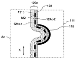
図8に、本発明の実施の形態3に係る三次元電子回路装置の要部平面図を示す。図8のAc部は図2のAa部に相当する。また図9(b)に本実施の形態で使用するシート状部材121cの一部の断面図を示す。
図10に、本発明の実施の形態4に係る三次元電子回路装置に用いるシート状部材121dの一部の断面図を示す。前述した実施の形態1では、シート状部材121aの金属電極122を有する面と反対側の面に溝を設けることにより、一方の面側に湾曲し易い性質を付加した。これに対し本実施の形態では、シート状部材121dを縦弾性係数の異なる第1および第2の部材125、126の2層構造としている。すなわち、表面に金属電極122が配された第1の部材125の縦弾性係数よりも第2の部材126の縦弾性係数を大きくすることで、第2の部材126側に湾曲し易い性質を付加している。
111、112 回路基板
113 半導体チップ
114 電子部品
115 端面電極
116 ベアチップ
117 配線パターン
120a〜120c 連結部材
121a〜121d シート状部材
122 金属細線
123 異方性導電フィルム
124a〜124c 溝
Claims (7)
- 主面が重なるように多層に配置された、電子部品が実装された複数の回路基板同士をそれらの端面で互いに電気的に接続した三次元回路装置であって、
前記各回路基板の端面は、第一のピッチ間隔で配設された複数の端面電極を有し、
前記各回路基板の前記端面電極は、前記多層方向において、連結部材を介して電気的に接続されており、
前記連結部材は、前記端面電極の表面同士を接続する異方性導電部材と、前記異方性導電部材に接しているシート状部材とを含み、
前記シート状部材の表面に前記第一のピッチ間隔よりも狭い第二のピッチ間隔で断続的に配列された、前記多層方向に延在する複数の導線を有し、
前記異方性導電部材と少なくとも一本の前記導線とが接している三次元電子回路装置。 - 1つの前記端面電極に前記導線が2本以上通過する請求項1に記載の三次元電子回路装置。
- 前記端面電極の断面形状は円弧であり、
前記第二のピッチ間隔は前記円弧の内周の長さの1/2未満である請求項1または2に記載の三次元電子回路装置。 - 前記シート状部材は、前記導線が配された面と異なる面に複数の溝が形成されている請求項1〜3のいずれか1項に記載の三次元電子回路装置。
- 前記溝は、前記導線の延在する方向と平行に形成されている請求項4に記載の三次元電子回路装置。
- 前記シート状部材は、前記導線が配された面と反対側の面に複数の空孔が形成されている請求項1〜5のいずれか1項に記載の三次元電子回路装置。
- 前記シート状部材の前記導線が配された面のうち、前記複数の導線の間に、前記導線と平行に溝が形成されている請求項1〜6のいずれか1項に記載の三次元電子回路装置。
Priority Applications (1)
| Application Number | Priority Date | Filing Date | Title |
|---|---|---|---|
| JP2007109192A JP4954778B2 (ja) | 2007-04-18 | 2007-04-18 | 三次元電子回路装置および連結部材 |
Applications Claiming Priority (1)
| Application Number | Priority Date | Filing Date | Title |
|---|---|---|---|
| JP2007109192A JP4954778B2 (ja) | 2007-04-18 | 2007-04-18 | 三次元電子回路装置および連結部材 |
Publications (2)
| Publication Number | Publication Date |
|---|---|
| JP2008270409A JP2008270409A (ja) | 2008-11-06 |
| JP4954778B2 true JP4954778B2 (ja) | 2012-06-20 |
Family
ID=40049549
Family Applications (1)
| Application Number | Title | Priority Date | Filing Date |
|---|---|---|---|
| JP2007109192A Expired - Fee Related JP4954778B2 (ja) | 2007-04-18 | 2007-04-18 | 三次元電子回路装置および連結部材 |
Country Status (1)
| Country | Link |
|---|---|
| JP (1) | JP4954778B2 (ja) |
Families Citing this family (1)
| Publication number | Priority date | Publication date | Assignee | Title |
|---|---|---|---|---|
| KR100969695B1 (ko) | 2008-03-31 | 2010-07-14 | 르네사스 일렉트로닉스 가부시키가이샤 | 동작모드를 스위칭할 수 있는 반도체장치 |
Family Cites Families (6)
| Publication number | Priority date | Publication date | Assignee | Title |
|---|---|---|---|---|
| JPH0422075A (ja) * | 1990-05-17 | 1992-01-27 | Seiko Epson Corp | 配線接続装置 |
| JPH05343844A (ja) * | 1992-06-04 | 1993-12-24 | Toshiba Corp | 非可撓性回路基板と可撓性回路基板との電気的な接続方法 |
| JP2000138425A (ja) * | 1998-11-02 | 2000-05-16 | Toshiba Corp | 接続配線構造 |
| JP3327252B2 (ja) * | 1999-05-20 | 2002-09-24 | 日本電気株式会社 | テープキャリア、tcpおよび液晶表示装置 |
| JP2001326441A (ja) * | 2000-05-17 | 2001-11-22 | Sony Corp | 複合配線板及びその製造方法 |
| JP4879276B2 (ja) * | 2006-10-24 | 2012-02-22 | パナソニック株式会社 | 3次元電子回路装置 |
-
2007
- 2007-04-18 JP JP2007109192A patent/JP4954778B2/ja not_active Expired - Fee Related
Also Published As
| Publication number | Publication date |
|---|---|
| JP2008270409A (ja) | 2008-11-06 |
Similar Documents
| Publication | Publication Date | Title |
|---|---|---|
| US7816782B2 (en) | Wiring substrate for mounting semiconductors, method of manufacturing the same, and semiconductor package | |
| US9024203B2 (en) | Embedded printed circuit board and method for manufacturing same | |
| JP4879276B2 (ja) | 3次元電子回路装置 | |
| CN107770947A (zh) | 印刷布线板和印刷布线板的制造方法 | |
| CN108307584B (zh) | 元器件模块 | |
| JP2013089847A (ja) | プリント基板およびそれを用いた電子機器 | |
| US20190254164A1 (en) | Circuit board, method of manufacturing circuit board, and electronic device | |
| EP2273858A1 (en) | Printed circuit board unit and electronic device | |
| JP4766050B2 (ja) | 電子回路装置の製造方法 | |
| CN101499453B (zh) | 配线电路基板及其制造方法 | |
| US9929116B2 (en) | Electronic device module and method of manufacturing the same | |
| JP4954778B2 (ja) | 三次元電子回路装置および連結部材 | |
| JP6863244B2 (ja) | 電子部品および電子部品の製造方法 | |
| JP2010034119A (ja) | 半導体装置 | |
| JP2008118155A (ja) | 半導体装置用パッケージ | |
| JP4954781B2 (ja) | 三次元電子回路装置 | |
| JP2004266271A (ja) | 電子部品の実装体及びその製造方法 | |
| US20150016069A1 (en) | Printed circuit board | |
| JP4667154B2 (ja) | 配線基板、電気素子装置並びに複合基板 | |
| US20110000704A1 (en) | Printed Circuit Board and Method of Manufacturing the Same | |
| JP4699089B2 (ja) | チップオンフィルム半導体装置 | |
| CN211152313U (zh) | 电气元件及电子设备 | |
| JP2009272510A (ja) | Icパッケージの実装構造、その製造方法およびそのためのシートキャパシタ | |
| WO2017038791A1 (ja) | 樹脂回路基板、部品搭載樹脂回路基板 | |
| US20060205243A1 (en) | Pitch converting connector and method of manufacture thereof |
Legal Events
| Date | Code | Title | Description |
|---|---|---|---|
| RD04 | Notification of resignation of power of attorney |
Free format text: JAPANESE INTERMEDIATE CODE: A7424 Effective date: 20081107 |
|
| A621 | Written request for application examination |
Free format text: JAPANESE INTERMEDIATE CODE: A621 Effective date: 20091126 |
|
| A977 | Report on retrieval |
Free format text: JAPANESE INTERMEDIATE CODE: A971007 Effective date: 20110921 |
|
| A131 | Notification of reasons for refusal |
Free format text: JAPANESE INTERMEDIATE CODE: A131 Effective date: 20110929 |
|
| A521 | Written amendment |
Free format text: JAPANESE INTERMEDIATE CODE: A523 Effective date: 20111125 |
|
| TRDD | Decision of grant or rejection written | ||
| A01 | Written decision to grant a patent or to grant a registration (utility model) |
Free format text: JAPANESE INTERMEDIATE CODE: A01 Effective date: 20120216 |
|
| A01 | Written decision to grant a patent or to grant a registration (utility model) |
Free format text: JAPANESE INTERMEDIATE CODE: A01 |
|
| A61 | First payment of annual fees (during grant procedure) |
Free format text: JAPANESE INTERMEDIATE CODE: A61 Effective date: 20120314 |
|
| R150 | Certificate of patent or registration of utility model |
Free format text: JAPANESE INTERMEDIATE CODE: R150 |
|
| FPAY | Renewal fee payment (event date is renewal date of database) |
Free format text: PAYMENT UNTIL: 20150323 Year of fee payment: 3 |
|
| LAPS | Cancellation because of no payment of annual fees |