JP4902950B2 - Led照明光源 - Google Patents
Led照明光源 Download PDFInfo
- Publication number
- JP4902950B2 JP4902950B2 JP2004259304A JP2004259304A JP4902950B2 JP 4902950 B2 JP4902950 B2 JP 4902950B2 JP 2004259304 A JP2004259304 A JP 2004259304A JP 2004259304 A JP2004259304 A JP 2004259304A JP 4902950 B2 JP4902950 B2 JP 4902950B2
- Authority
- JP
- Japan
- Prior art keywords
- led
- light source
- led element
- outer peripheral
- illumination light
- Prior art date
- Legal status (The legal status is an assumption and is not a legal conclusion. Google has not performed a legal analysis and makes no representation as to the accuracy of the status listed.)
- Expired - Fee Related
Links
Images


Classifications
-
- F—MECHANICAL ENGINEERING; LIGHTING; HEATING; WEAPONS; BLASTING
- F21—LIGHTING
- F21L—LIGHTING DEVICES OR SYSTEMS THEREOF, BEING PORTABLE OR SPECIALLY ADAPTED FOR TRANSPORTATION
- F21L4/00—Electric lighting devices with self-contained electric batteries or cells
- F21L4/02—Electric lighting devices with self-contained electric batteries or cells characterised by the provision of two or more light sources
- F21L4/022—Pocket lamps
- F21L4/027—Pocket lamps the light sources being a LED
-
- F—MECHANICAL ENGINEERING; LIGHTING; HEATING; WEAPONS; BLASTING
- F21—LIGHTING
- F21S—NON-PORTABLE LIGHTING DEVICES; SYSTEMS THEREOF; VEHICLE LIGHTING DEVICES SPECIALLY ADAPTED FOR VEHICLE EXTERIORS
- F21S6/00—Lighting devices intended to be free-standing
-
- F—MECHANICAL ENGINEERING; LIGHTING; HEATING; WEAPONS; BLASTING
- F21—LIGHTING
- F21Y—INDEXING SCHEME ASSOCIATED WITH SUBCLASSES F21K, F21L, F21S and F21V, RELATING TO THE FORM OR THE KIND OF THE LIGHT SOURCES OR OF THE COLOUR OF THE LIGHT EMITTED
- F21Y2115/00—Light-generating elements of semiconductor light sources
- F21Y2115/10—Light-emitting diodes [LED]
-
- H—ELECTRICITY
- H01—ELECTRIC ELEMENTS
- H01L—SEMICONDUCTOR DEVICES NOT COVERED BY CLASS H10
- H01L2224/00—Indexing scheme for arrangements for connecting or disconnecting semiconductor or solid-state bodies and methods related thereto as covered by H01L24/00
- H01L2224/01—Means for bonding being attached to, or being formed on, the surface to be connected, e.g. chip-to-package, die-attach, "first-level" interconnects; Manufacturing methods related thereto
- H01L2224/42—Wire connectors; Manufacturing methods related thereto
- H01L2224/47—Structure, shape, material or disposition of the wire connectors after the connecting process
- H01L2224/48—Structure, shape, material or disposition of the wire connectors after the connecting process of an individual wire connector
- H01L2224/4805—Shape
- H01L2224/4809—Loop shape
- H01L2224/48091—Arched
-
- H—ELECTRICITY
- H01—ELECTRIC ELEMENTS
- H01L—SEMICONDUCTOR DEVICES NOT COVERED BY CLASS H10
- H01L2224/00—Indexing scheme for arrangements for connecting or disconnecting semiconductor or solid-state bodies and methods related thereto as covered by H01L24/00
- H01L2224/01—Means for bonding being attached to, or being formed on, the surface to be connected, e.g. chip-to-package, die-attach, "first-level" interconnects; Manufacturing methods related thereto
- H01L2224/42—Wire connectors; Manufacturing methods related thereto
- H01L2224/47—Structure, shape, material or disposition of the wire connectors after the connecting process
- H01L2224/48—Structure, shape, material or disposition of the wire connectors after the connecting process of an individual wire connector
- H01L2224/481—Disposition
- H01L2224/48151—Connecting between a semiconductor or solid-state body and an item not being a semiconductor or solid-state body, e.g. chip-to-substrate, chip-to-passive
- H01L2224/48221—Connecting between a semiconductor or solid-state body and an item not being a semiconductor or solid-state body, e.g. chip-to-substrate, chip-to-passive the body and the item being stacked
- H01L2224/48245—Connecting between a semiconductor or solid-state body and an item not being a semiconductor or solid-state body, e.g. chip-to-substrate, chip-to-passive the body and the item being stacked the item being metallic
- H01L2224/48247—Connecting between a semiconductor or solid-state body and an item not being a semiconductor or solid-state body, e.g. chip-to-substrate, chip-to-passive the body and the item being stacked the item being metallic connecting the wire to a bond pad of the item
-
- H—ELECTRICITY
- H01—ELECTRIC ELEMENTS
- H01L—SEMICONDUCTOR DEVICES NOT COVERED BY CLASS H10
- H01L2224/00—Indexing scheme for arrangements for connecting or disconnecting semiconductor or solid-state bodies and methods related thereto as covered by H01L24/00
- H01L2224/01—Means for bonding being attached to, or being formed on, the surface to be connected, e.g. chip-to-package, die-attach, "first-level" interconnects; Manufacturing methods related thereto
- H01L2224/42—Wire connectors; Manufacturing methods related thereto
- H01L2224/47—Structure, shape, material or disposition of the wire connectors after the connecting process
- H01L2224/48—Structure, shape, material or disposition of the wire connectors after the connecting process of an individual wire connector
- H01L2224/481—Disposition
- H01L2224/48151—Connecting between a semiconductor or solid-state body and an item not being a semiconductor or solid-state body, e.g. chip-to-substrate, chip-to-passive
- H01L2224/48221—Connecting between a semiconductor or solid-state body and an item not being a semiconductor or solid-state body, e.g. chip-to-substrate, chip-to-passive the body and the item being stacked
- H01L2224/48245—Connecting between a semiconductor or solid-state body and an item not being a semiconductor or solid-state body, e.g. chip-to-substrate, chip-to-passive the body and the item being stacked the item being metallic
- H01L2224/48257—Connecting between a semiconductor or solid-state body and an item not being a semiconductor or solid-state body, e.g. chip-to-substrate, chip-to-passive the body and the item being stacked the item being metallic connecting the wire to a die pad of the item
-
- H—ELECTRICITY
- H01—ELECTRIC ELEMENTS
- H01L—SEMICONDUCTOR DEVICES NOT COVERED BY CLASS H10
- H01L2224/00—Indexing scheme for arrangements for connecting or disconnecting semiconductor or solid-state bodies and methods related thereto as covered by H01L24/00
- H01L2224/01—Means for bonding being attached to, or being formed on, the surface to be connected, e.g. chip-to-package, die-attach, "first-level" interconnects; Manufacturing methods related thereto
- H01L2224/42—Wire connectors; Manufacturing methods related thereto
- H01L2224/47—Structure, shape, material or disposition of the wire connectors after the connecting process
- H01L2224/49—Structure, shape, material or disposition of the wire connectors after the connecting process of a plurality of wire connectors
- H01L2224/491—Disposition
- H01L2224/49105—Connecting at different heights
- H01L2224/49107—Connecting at different heights on the semiconductor or solid-state body
Landscapes
- Non-Portable Lighting Devices Or Systems Thereof (AREA)
- Planar Illumination Modules (AREA)
- Led Device Packages (AREA)
- Fastening Of Light Sources Or Lamp Holders (AREA)
- Arrangement Of Elements, Cooling, Sealing, Or The Like Of Lighting Devices (AREA)
Description
まず、図10および図11を参照しながら、本実施形態に係るLED照明光源100について説明する。
次に、本発明によるLED照明光源の第2の実施形態を説明する。
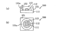
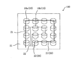
11 基板
12 LED素子
13 蛍光体樹脂部
14 レンズ
15 開口部
20 配線回路
21 第1の配線パターン
22 第2の配線パターン
23 抵抗素子
30 調光器
31 商用電源
32 ヒューズ
33 電源トランス
34 ダイオードブリッジ
35 平滑コンデンサ
36 レギュレータ
37、38 端子
40 金属板
41 多層配線基板
42 配線パターン
43 ビア
45 アンダーフィル(応力緩和層)
50 スキージ
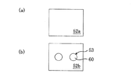
51 印刷版
51a 開口部(貫通孔)
60 樹脂ペースト
52 印刷板
53 開口部
55 版
56 感光性樹脂膜
57 開口部
58 ディスペンサー
59 注射器
120 給電部
130 コネクタ
131 ガイド部
132 ライン
133 点灯装置
135 台
136 ダイヤル
150 照明スタンド
151 反射板
151a 反射面
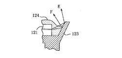
160 懐中電灯
162 ON−OFFスイッチ
164 グレア防止スイッチ
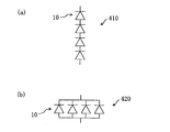
100 LED照明光源
200、300、400 LED照明光源
Claims (10)
- 基板と、
前記基板上に二次元的に配列された複数のLED素子と、
前記複数のLED素子に電気的に接続された配線回路と
を備え、
前記配線回路は、二次元的に配列された前記複数のLED素子のうち、外周部に位置する少なくとも1つのLED素子と、前記外周部以外の領域に位置する少なくとも1つのLED素子に対して、別々に駆動電流を供給できる配線構造を有しており、
前記複数のLED素子のそれぞれには、各LED素子の配光特性を制御するレンズが設けられており、
前記外周部以外に位置する各LED素子に設けられた前記レンズは、前記外周部に位置する各LED素子に設けられた前記レンズよりも、狭角の配光を実現するレンズ構造を有しており、
前記駆動電流の調節により、前記外周部に位置する少なくとも1つのLED素子を減光させる
LED照明光源。 - 前記配線回路は、前記外周部に位置する複数のLED素子を電気的に接続する第1の配線パターンと、前記外周部以外の領域に位置する複数のLED素子を電気的に接続する第2の配線パターンとを有している、請求項1に記載のLED照明光源。
- 前記配線回路は、調光器に電気的に接続されており、
前記調光器は、前記第1の配線パターンに電気的に接続されたLED素子の調光と、前記第2の配線パターンに電気的に接続されたLED素子の調光とを、独立して行なう機能を有している、請求項2に記載のLED照明光源。 - 前記配線回路における前記第1の配線パターンは、調光器に電気的に接続されており、
前記調光器は、前記第1の配線パターンに電気的に接続されたLED素子の調光を行なう機能を有している、請求項2に記載のLED照明光源。 - 前記第1の配線パターンおよび第2の配線パターンの少なくとも一方に接続された抵抗素子を更に備え、
前記抵抗素子は、前記第1の配線パターンを流れる電流の大きさと前記第2の配線パターンを流れる電流の大きさとの間の差異を、前記抵抗素子が存在しない場合に比べて減少させる、請求項2から4の何れかに記載のLED照明光源。 - 前記複数のLED素子のそれぞれは、ベアチップLEDと、前記ベアチップLEDを覆う蛍光体樹脂部とを有しており、
前記蛍光体樹脂部は、前記ベアチップLEDから出射された光を当該光の波長よりも長い波長の光に変換する蛍光体と、前記蛍光体を分散させる樹脂とから構成されている、請求項1から5の何れかに記載のLED照明光源。 - 前記外周部は、前記二次元的に配列された複数のLED素子の最外周に位置する領域である、請求項1から5の何れかに記載のLED照明光源。
- 前記外周部に位置する少なくとも1つのLED素子を減光させる際に、前記外周部以外に位置する少なくとも1つのLED素子の光を一定にする
請求項1に記載のLED照明光源。 - LED照明光源を用いた照明方法であって、
前記LED照明光源は、
基板と、
前記基板上に二次元的に配列された複数のLED素子と、
前記複数のLED素子に電気的に接続された配線回路と
を備え、
前記配線回路は、二次元的に配列された前記複数のLED素子のうち、外周部に位置する少なくとも1つのLED素子と、前記外周部以外の領域に位置する少なくとも1つのLED素子に対して、別々に駆動電流を供給できる配線構造を有しており、
前記複数のLED素子のそれぞれには、各LED素子の配光特性を制御するレンズが設けられており、
前記外周部以外に位置する各LED素子に設けられた前記レンズは、前記外周部に位置する各LED素子に設けられた前記レンズよりも、狭角の配光を実現するレンズ構造を有しており、
前記外周部に位置する少なくとも1つのLED素子に供給する駆動電流を調節することにより、前記外周部に位置する少なくとも1つのLED素子を減光させるLED照明光源の照明方法。 - 前記外周部に位置する少なくとも1つのLED素子に供給する駆動電流を調節して、減光させる際に、前記外周部以外に位置する少なくとも1つのLED素子に供給する駆動電流を一定にする
請求項9に記載のLED照明光源の照明方法。
Priority Applications (1)
| Application Number | Priority Date | Filing Date | Title |
|---|---|---|---|
| JP2004259304A JP4902950B2 (ja) | 2003-09-16 | 2004-09-07 | Led照明光源 |
Applications Claiming Priority (3)
| Application Number | Priority Date | Filing Date | Title |
|---|---|---|---|
| JP2003322645 | 2003-09-16 | ||
| JP2003322645 | 2003-09-16 | ||
| JP2004259304A JP4902950B2 (ja) | 2003-09-16 | 2004-09-07 | Led照明光源 |
Publications (3)
| Publication Number | Publication Date |
|---|---|
| JP2005117028A JP2005117028A (ja) | 2005-04-28 |
| JP2005117028A5 JP2005117028A5 (ja) | 2007-08-02 |
| JP4902950B2 true JP4902950B2 (ja) | 2012-03-21 |
Family
ID=34554437
Family Applications (1)
| Application Number | Title | Priority Date | Filing Date |
|---|---|---|---|
| JP2004259304A Expired - Fee Related JP4902950B2 (ja) | 2003-09-16 | 2004-09-07 | Led照明光源 |
Country Status (1)
| Country | Link |
|---|---|
| JP (1) | JP4902950B2 (ja) |
Families Citing this family (19)
| Publication number | Priority date | Publication date | Assignee | Title |
|---|---|---|---|---|
| JP2007018878A (ja) * | 2005-07-07 | 2007-01-25 | Matsushita Electric Works Ltd | 照明器具 |
| KR100691191B1 (ko) * | 2005-07-15 | 2007-03-09 | 삼성전기주식회사 | Led를 이용한 면광원 및 이를 구비하는 lcd 백라이트유닛 |
| JP4548668B2 (ja) * | 2005-10-21 | 2010-09-22 | タイテック株式会社 | 照明シート |
| JP4989936B2 (ja) * | 2006-07-27 | 2012-08-01 | 株式会社朝日ラバー | 照明装置 |
| EP3223313B1 (en) | 2007-01-22 | 2021-04-14 | Cree, Inc. | Monolithic light emitter having multiple light emitting sub-devices |
| JP4995120B2 (ja) * | 2008-02-28 | 2012-08-08 | シャープ株式会社 | 照明装置およびこれを備えた表示装置 |
| JP5180739B2 (ja) * | 2008-08-27 | 2013-04-10 | パナソニック株式会社 | バックライト装置 |
| WO2010061913A1 (ja) * | 2008-11-27 | 2010-06-03 | 京セラ株式会社 | 照明器具 |
| JP5327601B2 (ja) * | 2008-12-12 | 2013-10-30 | 東芝ライテック株式会社 | 発光モジュールおよび照明装置 |
| JP2010153044A (ja) * | 2008-12-23 | 2010-07-08 | Toshiba Lighting & Technology Corp | 光源ユニット及び照明器具 |
| KR101646256B1 (ko) * | 2009-12-29 | 2016-08-05 | 엘지이노텍 주식회사 | 발광장치 |
| JPWO2011108664A1 (ja) * | 2010-03-03 | 2013-06-27 | 有限会社Mtec | 光半導体装置 |
| JP2012028412A (ja) * | 2010-07-20 | 2012-02-09 | Furukawa Electric Co Ltd:The | 2次元面発光レーザアレイ素子、面発光レーザ装置および光源 |
| JP5341154B2 (ja) * | 2011-08-31 | 2013-11-13 | 株式会社フジクラ | 高演色性発光ダイオードランプユニット |
| JP5992674B2 (ja) | 2011-10-05 | 2016-09-14 | シチズン電子株式会社 | 発光モジュール |
| TWI446599B (zh) * | 2012-02-15 | 2014-07-21 | Polar Lights Opto Co Ltd | 無邊框的led晶片封裝方法及以該方法製成的發光裝置 |
| JP5946311B2 (ja) * | 2012-04-11 | 2016-07-06 | シチズンホールディングス株式会社 | Ledモジュール |
| JP7339581B2 (ja) * | 2018-12-20 | 2023-09-06 | 日亜化学工業株式会社 | 発光装置及び発光回路 |
| US11739910B2 (en) | 2019-12-16 | 2023-08-29 | Lumileds Llc | LED arrays with self-stabilizing torch functions |
Family Cites Families (5)
| Publication number | Priority date | Publication date | Assignee | Title |
|---|---|---|---|---|
| JPS6332972A (ja) * | 1986-07-26 | 1988-02-12 | Mitsubishi Cable Ind Ltd | ランプ |
| JPH01146248U (ja) * | 1988-03-29 | 1989-10-09 | ||
| JPH0744029Y2 (ja) * | 1990-12-28 | 1995-10-09 | 株式会社小糸製作所 | Ledモジュール |
| JPH11162234A (ja) * | 1997-11-25 | 1999-06-18 | Matsushita Electric Works Ltd | 発光ダイオードを用いた光源 |
| JP3989794B2 (ja) * | 2001-08-09 | 2007-10-10 | 松下電器産業株式会社 | Led照明装置およびled照明光源 |
-
2004
- 2004-09-07 JP JP2004259304A patent/JP4902950B2/ja not_active Expired - Fee Related
Also Published As
| Publication number | Publication date |
|---|---|
| JP2005117028A (ja) | 2005-04-28 |
Similar Documents
| Publication | Publication Date | Title |
|---|---|---|
| US7204607B2 (en) | LED lamp | |
| JP4902950B2 (ja) | Led照明光源 | |
| JP6342468B2 (ja) | 発光装置、および照明装置 | |
| JP6369784B2 (ja) | 発光装置、及びそれを用いた照明用光源及び照明装置 | |
| JP2005100800A (ja) | Led照明光源 | |
| CN109791968A (zh) | 发光二极管、组件和相关方法 | |
| US9799243B2 (en) | Lighting devices including solid state emitter groups for illuminating printed material with enhanced vibrancy | |
| JP2010534907A (ja) | 照明装置 | |
| JP5443959B2 (ja) | 照明装置 | |
| JP2010092993A (ja) | 照明装置 | |
| CN208489233U (zh) | Led光源器件及发光装置 | |
| JP2004103444A (ja) | 照明器具 | |
| EP2492898A2 (en) | Light Emitting Device | |
| JP6152726B2 (ja) | 照明装置及び照明装置の制御方法 | |
| TWI725302B (zh) | 照明器具 | |
| US20170005078A1 (en) | Light emitting device | |
| JP2017147072A (ja) | Ledモジュール | |
| JP6156796B2 (ja) | 照明装置及び照明装置の制御方法 | |
| JP2014187095A (ja) | Ledモジュールおよび照明装置 | |
| JP2020119723A (ja) | 発光モジュール、および照明装置 | |
| CN110504246A (zh) | 发光器件及发光装置 | |
| CN210535666U (zh) | 双基色低蓝光的白色led元件以及白色led组件 | |
| JP7236659B2 (ja) | 照明装置及び照明装置の製造方法 | |
| TWI725301B (zh) | 照明器具 | |
| JP3209026U (ja) | 光半導体装置 |
Legal Events
| Date | Code | Title | Description |
|---|---|---|---|
| A521 | Written amendment |
Free format text: JAPANESE INTERMEDIATE CODE: A523 Effective date: 20070619 |
|
| A621 | Written request for application examination |
Free format text: JAPANESE INTERMEDIATE CODE: A621 Effective date: 20070619 |
|
| A977 | Report on retrieval |
Free format text: JAPANESE INTERMEDIATE CODE: A971007 Effective date: 20100119 |
|
| A131 | Notification of reasons for refusal |
Free format text: JAPANESE INTERMEDIATE CODE: A131 Effective date: 20100518 |
|
| A521 | Written amendment |
Free format text: JAPANESE INTERMEDIATE CODE: A523 Effective date: 20100714 |
|
| A02 | Decision of refusal |
Free format text: JAPANESE INTERMEDIATE CODE: A02 Effective date: 20100907 |
|
| A521 | Written amendment |
Free format text: JAPANESE INTERMEDIATE CODE: A523 Effective date: 20101202 |
|
| A911 | Transfer to examiner for re-examination before appeal (zenchi) |
Free format text: JAPANESE INTERMEDIATE CODE: A911 Effective date: 20101208 |
|
| A912 | Re-examination (zenchi) completed and case transferred to appeal board |
Free format text: JAPANESE INTERMEDIATE CODE: A912 Effective date: 20110121 |
|
| A521 | Written amendment |
Free format text: JAPANESE INTERMEDIATE CODE: A523 Effective date: 20111115 |
|
| A01 | Written decision to grant a patent or to grant a registration (utility model) |
Free format text: JAPANESE INTERMEDIATE CODE: A01 |
|
| A61 | First payment of annual fees (during grant procedure) |
Free format text: JAPANESE INTERMEDIATE CODE: A61 Effective date: 20120104 |
|
| R150 | Certificate of patent or registration of utility model |
Ref document number: 4902950 Country of ref document: JP Free format text: JAPANESE INTERMEDIATE CODE: R150 Free format text: JAPANESE INTERMEDIATE CODE: R150 |
|
| FPAY | Renewal fee payment (event date is renewal date of database) |
Free format text: PAYMENT UNTIL: 20150113 Year of fee payment: 3 |
|
| R250 | Receipt of annual fees |
Free format text: JAPANESE INTERMEDIATE CODE: R250 |
|
| R250 | Receipt of annual fees |
Free format text: JAPANESE INTERMEDIATE CODE: R250 |
|
| LAPS | Cancellation because of no payment of annual fees |