JP4902950B2 - LED lighting source - Google Patents
LED lighting source Download PDFInfo
- Publication number
- JP4902950B2 JP4902950B2 JP2004259304A JP2004259304A JP4902950B2 JP 4902950 B2 JP4902950 B2 JP 4902950B2 JP 2004259304 A JP2004259304 A JP 2004259304A JP 2004259304 A JP2004259304 A JP 2004259304A JP 4902950 B2 JP4902950 B2 JP 4902950B2
- Authority
- JP
- Japan
- Prior art keywords
- led
- light source
- led element
- outer peripheral
- illumination light
- Prior art date
- Legal status (The legal status is an assumption and is not a legal conclusion. Google has not performed a legal analysis and makes no representation as to the accuracy of the status listed.)
- Expired - Fee Related
Links
Images


Classifications
-
- F—MECHANICAL ENGINEERING; LIGHTING; HEATING; WEAPONS; BLASTING
- F21—LIGHTING
- F21L—LIGHTING DEVICES OR SYSTEMS THEREOF, BEING PORTABLE OR SPECIALLY ADAPTED FOR TRANSPORTATION
- F21L4/00—Electric lighting devices with self-contained electric batteries or cells
- F21L4/02—Electric lighting devices with self-contained electric batteries or cells characterised by the provision of two or more light sources
- F21L4/022—Pocket lamps
- F21L4/027—Pocket lamps the light sources being a LED
-
- F—MECHANICAL ENGINEERING; LIGHTING; HEATING; WEAPONS; BLASTING
- F21—LIGHTING
- F21S—NON-PORTABLE LIGHTING DEVICES; SYSTEMS THEREOF; VEHICLE LIGHTING DEVICES SPECIALLY ADAPTED FOR VEHICLE EXTERIORS
- F21S6/00—Lighting devices intended to be free-standing
-
- F—MECHANICAL ENGINEERING; LIGHTING; HEATING; WEAPONS; BLASTING
- F21—LIGHTING
- F21Y—INDEXING SCHEME ASSOCIATED WITH SUBCLASSES F21K, F21L, F21S and F21V, RELATING TO THE FORM OR THE KIND OF THE LIGHT SOURCES OR OF THE COLOUR OF THE LIGHT EMITTED
- F21Y2115/00—Light-generating elements of semiconductor light sources
- F21Y2115/10—Light-emitting diodes [LED]
-
- H—ELECTRICITY
- H01—ELECTRIC ELEMENTS
- H01L—SEMICONDUCTOR DEVICES NOT COVERED BY CLASS H10
- H01L2224/00—Indexing scheme for arrangements for connecting or disconnecting semiconductor or solid-state bodies and methods related thereto as covered by H01L24/00
- H01L2224/01—Means for bonding being attached to, or being formed on, the surface to be connected, e.g. chip-to-package, die-attach, "first-level" interconnects; Manufacturing methods related thereto
- H01L2224/42—Wire connectors; Manufacturing methods related thereto
- H01L2224/47—Structure, shape, material or disposition of the wire connectors after the connecting process
- H01L2224/48—Structure, shape, material or disposition of the wire connectors after the connecting process of an individual wire connector
- H01L2224/4805—Shape
- H01L2224/4809—Loop shape
- H01L2224/48091—Arched
-
- H—ELECTRICITY
- H01—ELECTRIC ELEMENTS
- H01L—SEMICONDUCTOR DEVICES NOT COVERED BY CLASS H10
- H01L2224/00—Indexing scheme for arrangements for connecting or disconnecting semiconductor or solid-state bodies and methods related thereto as covered by H01L24/00
- H01L2224/01—Means for bonding being attached to, or being formed on, the surface to be connected, e.g. chip-to-package, die-attach, "first-level" interconnects; Manufacturing methods related thereto
- H01L2224/42—Wire connectors; Manufacturing methods related thereto
- H01L2224/47—Structure, shape, material or disposition of the wire connectors after the connecting process
- H01L2224/48—Structure, shape, material or disposition of the wire connectors after the connecting process of an individual wire connector
- H01L2224/481—Disposition
- H01L2224/48151—Connecting between a semiconductor or solid-state body and an item not being a semiconductor or solid-state body, e.g. chip-to-substrate, chip-to-passive
- H01L2224/48221—Connecting between a semiconductor or solid-state body and an item not being a semiconductor or solid-state body, e.g. chip-to-substrate, chip-to-passive the body and the item being stacked
- H01L2224/48245—Connecting between a semiconductor or solid-state body and an item not being a semiconductor or solid-state body, e.g. chip-to-substrate, chip-to-passive the body and the item being stacked the item being metallic
- H01L2224/48247—Connecting between a semiconductor or solid-state body and an item not being a semiconductor or solid-state body, e.g. chip-to-substrate, chip-to-passive the body and the item being stacked the item being metallic connecting the wire to a bond pad of the item
-
- H—ELECTRICITY
- H01—ELECTRIC ELEMENTS
- H01L—SEMICONDUCTOR DEVICES NOT COVERED BY CLASS H10
- H01L2224/00—Indexing scheme for arrangements for connecting or disconnecting semiconductor or solid-state bodies and methods related thereto as covered by H01L24/00
- H01L2224/01—Means for bonding being attached to, or being formed on, the surface to be connected, e.g. chip-to-package, die-attach, "first-level" interconnects; Manufacturing methods related thereto
- H01L2224/42—Wire connectors; Manufacturing methods related thereto
- H01L2224/47—Structure, shape, material or disposition of the wire connectors after the connecting process
- H01L2224/48—Structure, shape, material or disposition of the wire connectors after the connecting process of an individual wire connector
- H01L2224/481—Disposition
- H01L2224/48151—Connecting between a semiconductor or solid-state body and an item not being a semiconductor or solid-state body, e.g. chip-to-substrate, chip-to-passive
- H01L2224/48221—Connecting between a semiconductor or solid-state body and an item not being a semiconductor or solid-state body, e.g. chip-to-substrate, chip-to-passive the body and the item being stacked
- H01L2224/48245—Connecting between a semiconductor or solid-state body and an item not being a semiconductor or solid-state body, e.g. chip-to-substrate, chip-to-passive the body and the item being stacked the item being metallic
- H01L2224/48257—Connecting between a semiconductor or solid-state body and an item not being a semiconductor or solid-state body, e.g. chip-to-substrate, chip-to-passive the body and the item being stacked the item being metallic connecting the wire to a die pad of the item
-
- H—ELECTRICITY
- H01—ELECTRIC ELEMENTS
- H01L—SEMICONDUCTOR DEVICES NOT COVERED BY CLASS H10
- H01L2224/00—Indexing scheme for arrangements for connecting or disconnecting semiconductor or solid-state bodies and methods related thereto as covered by H01L24/00
- H01L2224/01—Means for bonding being attached to, or being formed on, the surface to be connected, e.g. chip-to-package, die-attach, "first-level" interconnects; Manufacturing methods related thereto
- H01L2224/42—Wire connectors; Manufacturing methods related thereto
- H01L2224/47—Structure, shape, material or disposition of the wire connectors after the connecting process
- H01L2224/49—Structure, shape, material or disposition of the wire connectors after the connecting process of a plurality of wire connectors
- H01L2224/491—Disposition
- H01L2224/49105—Connecting at different heights
- H01L2224/49107—Connecting at different heights on the semiconductor or solid-state body
Description
本発明は、LED照明光源に関し、特に、一般照明用の白色LED照明光源に関する。 The present invention relates to an LED illumination light source, and more particularly to a white LED illumination light source for general illumination.
発光ダイオード素子(以下、「LED素子」と称する。)は、小型で効率が良く鮮やかな色の発光を示す半導体素子であり、その発光は優れた単色性ピークを有している。LED素子を用いて白色発光を得るには、赤色LED素子と緑色LED素子と青色LED素子とを近接して配置させ、拡散混色を行わせる照明光源が開発された。しかし、このような照明光源には、各LED素子が優れた単色性ピークを示すため、色ムラが生じやすいという問題がある。すなわち、各LED素子からの発光による混色が均一に行なわれない限り、白色発光に色ムラが生じてしまう。このような色ムラの問題を解消するために、青色LED素子と黄色蛍光体とを組み合わせて白色発光を得る照明光源が開発されている(例えば、特許文献1、特許文献2)。 A light-emitting diode element (hereinafter referred to as an “LED element”) is a semiconductor element that is small, efficient, and emits brightly colored light, and the light emission has an excellent monochromatic peak. In order to obtain white light emission using an LED element, an illumination light source has been developed in which a red LED element, a green LED element, and a blue LED element are arranged close to each other to perform diffusion color mixing. However, such an illumination light source has a problem that color unevenness is likely to occur because each LED element exhibits an excellent monochromatic peak. That is, unless the color mixture by light emission from each LED element is uniformly performed, color unevenness occurs in white light emission. In order to solve the problem of such color unevenness, an illumination light source has been developed that obtains white light emission by combining a blue LED element and a yellow phosphor (for example, Patent Document 1 and Patent Document 2).
特許文献1に開示されている技術によれば、青色LED素子からの発光と、その発光で励起され黄色を発光する黄色蛍光体からの発光とによって白色発光を得ている。この技術では、1種類のLED素子だけを用いて白色発光を得るので、複数種類のLED素子を近接させて白色発光を得る場合に生じる色ムラの問題を解消することができる。 According to the technique disclosed in Patent Document 1, white light emission is obtained by light emission from a blue LED element and light emission from a yellow phosphor that is excited by the light emission and emits yellow light. In this technique, since white light emission is obtained using only one type of LED element, the problem of color unevenness that occurs when white light emission is obtained by bringing a plurality of types of LED elements close to each other can be solved.
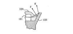
特許文献2に開示された砲弾型LED照明光源は、例えば図1に示す構成を有している。図1に示される砲弾型LED照明光源200は、LED素子121と、LED素子121をカバーする砲弾型の透明容器127と、LED素子121に電流を供給するためのリードフレーム122a、122bとを備えている。LED素子121が搭載されるフレーム122bのマウント部には、LED素子121の発光を矢印Dの方向に反射するカップ型反射板123が設けられている。LED素子121は、蛍光物質126が分散された第1の樹脂部124によって封止されており、第1の樹脂部124は、第2の樹脂部によって覆われている。LED素子121から青色が発光される場合、蛍光物質126が青色光の一部を黄色光に変換する。このため、青色光と黄色光が混じりあって白色光が得られることになる。
The bullet-type LED illumination light source disclosed in Patent Document 2 has, for example, the configuration shown in FIG. A bullet-type LED
1個のLED素子では、得られる光束が小さいため、今日、一般照明用光源として広く普及している白熱電球や蛍光ランプと同程度の光束を得るためには、複数のLED素子を配置してLED照明光源を構成することが望ましい。そのようなLED照明光源は、例えば特許文献3や特許文献4に開示されている。なお、関連する先行技術が特許文献5に開示されている。
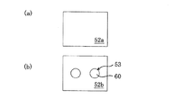
特許文献5は、特許文献2に開示された砲弾型LED照明光源が有する色ムラの問題を解決することができるLED照明光源を開示している。図1に示される砲弾型LED照明光源200によれば、図2に拡大して示すように、第1の樹脂部24はLED素子121を封止するようにカップ型反射板123内に充填させた後に硬化させて形成する関係上、第1の樹脂部24の上面に凹凸が生じやすく、その結果、蛍光物質126を含有する樹脂の厚さにムラが生じて、LED素子121からの光が第1の樹脂部124を通過する経路(例えば、光路E、F)上に存在する蛍光物質126の量がばらつき、色ムラを招くことになる。
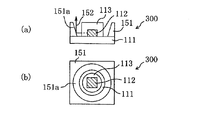
そのような問題を解消するために、特許文献5が開示するLED照明光源では、蛍光物質が分散された樹脂部の側面から、光反射部材(反射板)の反射面を離間させるように構成されている。図3(a)および(b)は、特許文献5に開示されたLED照明光源の一例を示す側面断面図および上面図である。図3(a)および(b)に示すLED照明光源300では、基板111に実装されたLED素子(ベアチップLED)112が、蛍光物質が分散された樹脂部113によって覆われている。基板111には、反射面151aを有する反射板151が貼り付けられており、そして、樹脂部113の側面と、反射板151の反射面151aとは離間して形成されている。樹脂部113の側面が反射板151の反射面151aと離間して形成されていることによって、反射板151の反射面151aの形状によって拘束されずに樹脂部113の形状を自由に設計することができ、その結果、色ムラを軽減する効果を発揮することができる。
In order to solve such a problem, the LED illumination light source disclosed in
図3に示す構成を複数個マトリクス状に配置すると、図4に示すようになる。図4に示すLED照明光源300では、LED素子112を覆う樹脂部113が基板111上に行列状に配列され、そして、各樹脂部113に対応する反射面151aを持った反射板151が基板111に貼り付けられる。このような構成にすると、複数個のLED素子の光束を利用できるので、今日広く普及している一般照明用光源(例えば、白熱電球や蛍光ランプ)と同程度の光束を得ることが容易となる。
When a plurality of the configurations shown in FIG. 3 are arranged in a matrix, the configuration is as shown in FIG. In the LED
図4に示すLED照明光源300を一般照明用光源として用いれば、色ムラもなく、また光束も十分なものが得られるのであるが、このLED照明光源300に対して本願発明者が更なる検討を加えた結果、次のようなことがわかった。従来はLED照明光源の光束を向上させることにばかり注意を払っていたが、光束が大きいLED照明光源(大光量LED照明光源)300は、観測者にとって不快なまぶしさ(グレア)が存在するという点である。つまり、一般照明用光源は、単に明るければ明るいほどよいというものではなく、観測者に不快な感じを与えることは好ましくない。
If the LED
グレアとは、視野内にある照明器具の輝度が高いことによって、視野内の輝度分布が不適切になって、不快に感じたり、細かいもの又は対象物を見る能力が低下する状態のことをいい(JIS C8106)、グレアが起きる条件としては、一般的に、(i)光源の輝度がある程度以上高い場合に、(ii)周囲が暗く、目が暗さになれているほどグレアを感じ、(iii)グレア源が視線に近いほど、(iv)また、グレア源の見かけの大きさが大きかったり、数が多いときにグレアを強く感じる。したがって、複数のLED素子からなるLED照明光源が高輝度で、かつ、そのLED照明光源を比較的暗いところで使用する場合には、グレアが起きやすくなると思われる。特に、LED照明光源は、LED素子から出射する光を用いているので、指向性が強く、蛍光ランプのような指向性の弱い光が観測者の目に入る場合と比較して、観測者は、LED照明光源によりグレアを感じてしまう場合が多い。かといって、グレア発生防止のために、LED照明光源の輝度を低下させてしまうと、一般照明用光源としては暗い光源となってしまう。また、グレアは周囲の条件にも影響を受けるので、グレアが発生しない条件のときにLED照明光源をわざわざ暗く点灯させる必要もない。そうすると、グレアが発生する条件を考慮して、グレア抑制の対策をとることができたり、また、通常通り明るく点灯できたりするLED照明光源があると非常に便利である。 Glare is a state in which the luminance distribution in the field of view is inappropriate due to the high luminance of the lighting fixture in the field of view, which makes it uncomfortable or reduces the ability to see fine objects or objects. (JIS C8106) As a condition for the occurrence of glare, generally, (i) when the luminance of the light source is higher than a certain level, (ii) the glare is felt as the surroundings are darker and the eyes are darkened. iii) The closer the glare source is to the line of sight, (iv) In addition, when the apparent size of the glare source is large or the number is large, the glare is strongly felt. Therefore, when the LED illumination light source composed of a plurality of LED elements has high luminance and the LED illumination light source is used in a relatively dark place, glare is likely to occur. In particular, since the LED illumination light source uses light emitted from the LED element, the observer has a higher directivity, and the observer has less directivity, such as a fluorescent lamp, entering the eyes of the observer. In many cases, glare is felt by the LED illumination light source. However, if the luminance of the LED illumination light source is lowered to prevent glare, it becomes a dark light source as a general illumination light source. In addition, since glare is affected by ambient conditions, it is not necessary to dimly light the LED illumination light source when glare does not occur. If it does so, it will be very convenient if there is an LED illumination light source that can take countermeasures for suppressing glare in consideration of the conditions for generating glare and can be lit brightly as usual.
本発明はかかる諸点に鑑みてなされたものであり、その主な目的は、グレアを抑制することができるLED照明光源を提供することにある。 The present invention has been made in view of such various points, and a main object thereof is to provide an LED illumination light source capable of suppressing glare.
本発明のLED照明光源は、基板と、前記基板上に二次元的に配列された複数のLED素子と、前記複数のLED素子に電気的に接続された配線回路とを備え、前記配線回路は、二次元的に配列された前記複数のLED素子のうち、外周部に位置する少なくとも1つのLED素子と、前記外周部以外の領域に位置する少なくとも1つLED素子に対して、別々に駆動電流を供給できる配線構造を有している。 The LED illumination light source of the present invention includes a substrate, a plurality of LED elements arranged two-dimensionally on the substrate, and a wiring circuit electrically connected to the plurality of LED elements, The driving current is separately applied to at least one LED element located in the outer peripheral portion and at least one LED element located in a region other than the outer peripheral portion among the plurality of LED elements arranged two-dimensionally. A wiring structure capable of supplying
好ましい実施形態において、前記配線回路は、前記外周部に位置する複数のLED素子を電気的に接続する第1の配線パターンと、前記外周部以外の領域に位置する複数のLED素子を電気的接続する第2の配線パターンとを有している。 In a preferred embodiment, the wiring circuit electrically connects a first wiring pattern that electrically connects a plurality of LED elements positioned on the outer peripheral portion and a plurality of LED elements positioned on a region other than the outer peripheral portion. And a second wiring pattern.
好ましい実施形態において、前記配線回路は、調光器に電気的に接続されており、前記調光器は、前記第1の配線パターンに電気的に接続されたLED素子の調光と、前記第2の配線パターンに電気的に接続されたLED素子の調光とを、独立して行なう機能を有している。 In a preferred embodiment, the wiring circuit is electrically connected to a dimmer, and the dimmer includes dimming of an LED element electrically connected to the first wiring pattern; It has the function to perform light control of the LED element electrically connected to 2 wiring patterns independently.
好ましい実施形態において、前記配線回路における前記第1の配線パターンは、調光器に電気的に接続されており、前記調光器は、前記第1の配線パターンに電気的に接続されたLED素子の調光を行なう機能を有している。 In a preferred embodiment, the first wiring pattern in the wiring circuit is electrically connected to a dimmer, and the dimmer is an LED element electrically connected to the first wiring pattern. It has a function to perform dimming.
好ましい実施形態において、前記第1の配線パターンおよび第2の配線パターンの少なくとも一方に接続された抵抗素子を更に備え、前記抵抗素子は、前記第1の配線パターンを流れる電流の大きさと前記第2の配線パターンを流れる電流の大きさとの間の差異を、前記抵抗素子が存在しない場合に比べて減少させる。 In a preferred embodiment, a resistance element connected to at least one of the first wiring pattern and the second wiring pattern is further included, and the resistance element has a magnitude of a current flowing through the first wiring pattern and the second wiring pattern. The difference between the magnitude of the current flowing through the wiring pattern is reduced as compared with the case where the resistance element is not present.
好ましい実施形態において、前記複数のLED素子のそれぞれは、ベアチップLEDと、前記ベアチップLEDを覆う蛍光体樹脂部とを有しており、前記蛍光体樹脂部は、前記ベアチップLEDから出射された光を当該光の波長よりも長い波長の光に変換する蛍光体と、前記蛍光体を分散させる樹脂とから構成されている。 In a preferred embodiment, each of the plurality of LED elements includes a bare chip LED and a phosphor resin portion that covers the bare chip LED, and the phosphor resin portion receives light emitted from the bare chip LED. It is comprised from the fluorescent substance converted into the light of the wavelength longer than the wavelength of the said light, and resin which disperse | distributes the said fluorescent substance.
好ましい実施形態において、前記外周部は、前記二次元的に配列された複数のLED素子の最外周に位置する領域である。 In preferable embodiment, the said outer peripheral part is an area | region located in the outermost periphery of the several LED element arranged in two dimensions.
好ましい実施形態において、前記複数のLED素子のそれぞれには、各LED素子の配光特性を制御するレンズが設けられており、前記外周部以外に位置する各LED素子に設けられた前記レンズは、前記外周部に位置する各LED素子に設けられた前記レンズよりも、狭角の配光を実現するレンズ構造を有している。 In a preferred embodiment, each of the plurality of LED elements is provided with a lens for controlling the light distribution characteristics of each LED element, and the lens provided in each LED element located other than the outer peripheral portion, It has a lens structure that realizes light distribution at a narrower angle than the lens provided in each LED element located on the outer periphery.
好ましい実施形態において、前記複数のLED素子のうち、前記外周部に位置する各LED素子が発する光の色温度は、前記外周部以外の各LED素子が発する光の色温度よりも低い。 In a preferred embodiment, among the plurality of LED elements, a color temperature of light emitted from each LED element located in the outer peripheral portion is lower than a color temperature of light emitted from each LED element other than the outer peripheral portion.
本発明のLED照明光源によれば、外周部に位置するLED素子の調光と、外周部以外の領域に位置するLED素子の調光とを、それぞれ独立して実行することができるため、グレアに影響を与える外周部のLED素子の輝度を選択的に変化させることができ、その結果、グレアの発生を効果的に抑制することができる。 According to the LED illumination light source of the present invention, the dimming of the LED elements located in the outer peripheral part and the dimming of the LED elements located in the area other than the outer peripheral part can be executed independently, It is possible to selectively change the luminance of the LED elements on the outer peripheral portion that affect the brightness, and as a result, it is possible to effectively suppress the occurrence of glare.
本発明の実施形態を説明する前に、図5から図8を参照しながら、複数のLED素子を点灯させる場合のLED照明光源の構成例を説明する。 Before describing an embodiment of the present invention, a configuration example of an LED illumination light source when a plurality of LED elements are turned on will be described with reference to FIGS. 5 to 8.
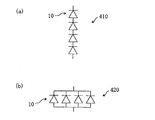
図5は、基板11上に4個のLED素子10が配列されたLED照明光源400を示している。図5のLED照明光源400では、4つのLED素子10を直列に接続すれば、図6(a)に示す回路410が形成される。一方、4つのLED素子10を並列に接続すれば、図6(b)に示す回路420が形成される。
FIG. 5 shows an LED
LED照明光源に含まれるLED素子10の数が多くなると、直列接続と並列接続とを組み合わせることも可能である。例えば、LED素子10を4×4=16個のマトリックス状に配列させたLED照明光源では、直列に接続した4個のLED素子10の組を並列に接続し、図7に示す回路430を形成することができる。並列に接続した4個のLED素子10の組を直接に接続すれば、図8に示す回路440を形成することができる。
When the number of
上記の回路400、420、430、440によれば、複数のLED素子10の各々が、相互に等しい光束の光を出射する。しかし、各LED素子10が同じ光束の光を出射しても、その光の全てが被照射物(例えば、LED照明光源が照明スタンドの用途に用いられる場合の本など)に向かうわけでない。光の拡散により、特定の被照射物(本など)に向かう光もあれば、周囲へと広がっていく光も生じる。
According to the
図9は、基板11上に4×4=16個のLED素子10を配列させたLED照明光源500の点灯した状態を模式的に示している。LED照明光源500におけるLED素子10は、図7の回路430を形成するように接続されていてもよいし、図8の回路440を形成するように接続されていてもよい。
FIG. 9 schematically shows a lighted state of the LED
図9に示すように、4行4列のマトリックス状に配列されたLED素子10のうち、外周部に位置するLED素子10aから放射された光Aは、内周部に位置するLED素子10bから放射された光Bに比べると、周囲に拡散しやすい。言い換えると、光Bは被照射物(本など)に向かいやすく、被照射物を照らす機能を充分に発揮するが、光Aは、その光を特に必要としていない観測者の目に届く可能性がある。このため、外周部に位置するLED素子10aから放射された光Aは、グレアを発生させる可能性が相対的に高くなる。
As shown in FIG. 9, among the
図9のLED照明光源500の場合、グレアを抑制するには、光Aのみならず、光Bの光束量も低減させる必要が生じる。これは、各LED素子10の光束が等しくなる回路構成が採用されているためである。すなわち、図7または図8の回路構成を採用する限り、外周部に位置するLED素子10aの光束だけ選択的に低減することができない。各LED素子10に供給する電流を一律に低減すると、被照射物を照らす光束が低下し、一般照明用光源としては暗い光源となってしまうため、都合が悪い。
In the case of the LED
そこで、本願発明者は、外周部に位置するLED素子10aと、内周部に位置するLED素子10bとを別回路で構成して、外周部のLED素子10aの輝度を選択的に調整できるようにすれば、グレアを効果的に抑制できることを想到し、本発明に至った。
Therefore, the inventor of the present application can selectively adjust the luminance of the
以下、図面を参照しながら、本発明の実施の形態を説明する。以下の図面においては、説明の簡潔化のため、実質的に同一の機能を有する構成要素を同一の参照符号で示す。なお、本発明は、以下の実施形態に限定されない。 Hereinafter, embodiments of the present invention will be described with reference to the drawings. In the following drawings, components having substantially the same function are denoted by the same reference numerals for the sake of brevity. The present invention is not limited to the following embodiment.
(実施形態1)
まず、図10および図11を参照しながら、本実施形態に係るLED照明光源100について説明する。
(Embodiment 1)
First, the LED
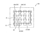
図10は、LED照明光源100の構成を模式的に示している。LED照明光源100は、基板11と、基板11上に二次元的に配列された複数のLED素子10と、複数のLED素子10に電気的に接続された配線回路20とを備えている。
FIG. 10 schematically shows the configuration of the LED
複数のLED素子10は、2次元的に密に配列されたLED素子の群(クラスタ)を形成している。LED素子の群(以下、「LED素子群」と称する。)に含まれる個々のLED素子10は、大きく2つのグループに分けられる。クラスタの外周部に位置するLED素子10aは第1のグループを形成し、クラスタの内周部に位置するLED素子10bは第2のグループを形成している。
The plurality of
本実施形態の配線回路20は、上記2つのLED素子グループに対応して、第1の配線パターン21と、第1の配線パターン21から独立した第2の配線パターン22とを備えている。外周部に位置する各LED素子10aは、第1の配線パターン21に電気的に接続されており、内周部の各LED素子10bは、第2の配線パターン22に電気的に接続されている。
The
本実施形態では、外周部に位置するLED素子10aと、それ以外(内周部)に位置するLED素子10bとを、それぞれ、別の配線パターン21、22に接続しているため、外周部のLED素子10aの輝度を選択的に変化させることができる。したがって、グレアの発生を効果的に抑制することができる。例えば、配線回路20を調光器(不図示)に電気的に接続して、その調光器によって、第1の配線パターン21に電気的に接続された各LED素子10aと、第2の配線パターン22に電気的に接続された各LED素子10bとをそれぞれ独立して調光するようにすれば、グレアの発生を抑制することができる。なお、第1の配線パターン21と第2の配線パターン22との両方を調光器に接続せずに、第1の配線パターン21だけを調光器(不図示)に電気的に接続して、LED素子10aだけを調光してもよい。
In the present embodiment, the
図11は、本実施形態におけるLED素子10の断面構成を模式的に示している。図11に示すように、LED素子10は、ベアチップLED12と、ベアチップLED12を覆う蛍光体樹脂部13とから構成されている。蛍光体樹脂部13は、ベアチップLED12から出射された光を当該光の波長よりも長い波長の光に変換する蛍光体(蛍光物質)と、蛍光体を分散させる樹脂とから構成されている。ベアチップLED12は、基板11に実装されており、そして、基板11には、図10に示す配線パターン21、22が形成されている。
FIG. 11 schematically shows a cross-sectional configuration of the
ベアチップLED12は、波長380nmから780nmの可視領域の範囲内にピーク波長を有する光を出射するLED素子である。蛍光体樹脂部13中に分散されている蛍光体は、波長380nから780nmの可視領域の範囲内で、ベアチップLED12のピーク波長とは異なるピーク波長を有する光を出射する蛍光体である。本実施形態におけるベアチップLED12は、青色の光を出射する青色LED素子であり、蛍光体樹脂部13に含有されている蛍光体は、黄色の光に変換する黄色蛍光体である。両者の光によって白色の光が形成される。
The
ベアチップLED12は、窒化ガリウム(GaN)系材料からなるLEDチップであり、例えば波長460nmの光を出射する。ベアチップLED12として青色を発するLEDチップを用いる場合、蛍光体としては、(Y・Sm)3(Al・Ga)5O12:Ce、(Y0.39Gd0.57Ce0.03Sm0.01)3Al5O12などを好適に用いることができる。本実施形態では、蛍光体樹脂部13は略円柱形状に形成されており、ベアチップLED12の寸法が、例えば約0.3mm×約0.3mmのときに、蛍光体樹脂部13の直径は例えば約0.7mm〜約0.9mmである。
The
図10の構成では、LED素子10が基板11上に4個×4個の行列状に配置されているが、LED素子10の数は図10の例に限定されず、N行×M列(N、M=2以上の整数)の配列であってもよい。
In the configuration of FIG. 10, the
また、LED素子10の二次元的配列は、図10に示すような行列状の配列に限らず、略同心円状の配列や、渦巻き状の配列であってもよい。そのような場合においても、専らグレアの発生の原因となる外周部に位置するLED素子10aを、配線パターン21に接続して、調光できるようにすればよい。
Further, the two-dimensional arrangement of the
図12は、LED素子10を8個×8個の行列状に配列させたLED照明光源100の回路構成図を示している。外周部に位置するLED素子10aは、第1の配線パターン21に接続されており、それ以外のLED素子10bは、第2の配線パターン22に接続されている。
FIG. 12 shows a circuit configuration diagram of the LED
図12の構成では、LED素子10aの数と、LED素子10bの数とが異なる。このため、第1の配線パターン21および第2の配線パターン22の各々を流れる電流の値を実質的に等しくするための抵抗素子23が第1の配線パターン21に接続されている。
In the configuration of FIG. 12, the number of
図13に示すように、LED素子10aとLED素子10bとの数を同じにすることも可能である。その場合、第1の配線パターン21および第2の配線パターン22の各々を流れる電流の値は、典型的には相互に等しくなるため、図12に示すような抵抗素子23を設ける必要性は低い。
As shown in FIG. 13, the number of
図14は、第1の配線パターン21に電気的に接続する調光器30の一例を示している。図14に示す調光器30は、商用電源(例えば、AC100V)31からの交流電圧を直流電圧に整流した後、レギュレータ36によって電力制御を行うことができる回路構成を有している。調光器30は、ヒューズ32と、電源トランス33と、ダイオードブリッジ34と、平滑コンデンサ35と、レギュレータ36とから構成されている。端子37は直流電圧(+)を出力し、端子38はグランドの電位を有している。
FIG. 14 shows an example of the dimmer 30 that is electrically connected to the
本発明の好ましい実施形態では、端子37、38が第1の配線パターン21に接続される。例えば、図12または図13に示す第1の配線パターン21のプラス側端部およびマイナス側端部を、それぞれ、調光器20の端子37、38に接続する。レギュレータ36により、第1の配線パターン21に接続されたLED素子10aに供給する電流の大きさを調節することにより、外周部に位置するLED素子10aの調光を行なうことができる。
In a preferred embodiment of the present invention, the
2台の調光器20を用意して、それぞれを第1の配線パターン21および第2の配線パターン22に接続してもよい。その場合、LED素子10a、10bの調光をそれぞれ独立して行なうことができる。なお、LED素子10(10a、10b)の調光を行なうための調光器は、図13に示す調光器30に限らず、他の構成を有する調光器を用いても良い。
Two
本実施形態のLED照明光源100にグレアが発生している状態のときには、調光器30によって外周部のLED素子10aの光を調整して、グレアを解消できる。このとき、LED素子10bの光はそのままにすることができるので、LED照明光源100の光束を低下されることなく、グレアを抑制することができる。
When the glare is generated in the LED
また、LED素子10bの光は、被照射物を専ら照らすことになる。ここで、「被照射物」とは、例えばLED照明光源100が照明スタンドの用途に用いられる場合の本などである。このため、LED照明光源100の光束が仮に大幅に低下したとしても、被照射物(本など)を見る場合には特に支障のない場合もあり得る。例えば、狭角の配向を実現するレンズがLED素子10bの前面に配置されていれば、被照射物を照らす光は主としてLED素子10bから放射されたものとなるため、調光のためにLED素子10aの光束を大幅に低減しても、被照射物を照らす光の強さを略一定に保持することができる。
Moreover, the light of the
また、調光器30を用いずに、LED素子10aをオン−オフさせるような構成を採用してもよい。LED素子10aをオフにすることによってグレアを抑制しつつ、LED素子10bからの光で被照射物を照射することができる。
Moreover, you may employ | adopt the structure which turns on and off the
なお、LED照明光源100の利用者が、外周部のLED素子10だけが暗い状態、または、不点灯の状態に違和感をいだく場合、LED素子10aとLED素子10bとの明るさの割合を自動的にまたは手動で制御する機構を採用し、それによって、そのような違和感を緩和するようにしてもよい。
In addition, when the user of the LED
本実施形態のLED照明光源100は、図15に示すようなカード型LED照明光源にすることもできる。図15に示すカード型LED照明光源100では、基板11に給電部120が設けられており、この給電部120は、基板11内に設けられた第1の配線パターン21および第2の配線パターン22を介して、LED素子10に電気的に接続されている(給電部120詳細は不図示)。給電部120の表面に給電端子を設けても良い。図15に示すカード型LED照明光源100を実際に使用する場合には、各LED素子10を収納する開口部を有する金属製の反射板(図4の反射板151を参照)を基板11の上に配置することが好適である。なお、基板11と反射板(151)の両方をあわせて、すなわち、反射板を含めて、LED照明光源100の「基板」と呼んでもよい。あるいは、基板11自体に反射面を作製して、その基板11を光学反射部材として用いることも可能である。
The LED
このカード型LED照明光源100は、図16に示すようにして用いることができる。図16は、反射板151を基板11に貼り付けた構成のLED照明光源100と、LED照明光源100が着脱可能に挿入されるコネクタ130と、コネクタ130を介してLED照明光源100と電気的に接続される点灯装置133とを示している。点灯装置133は、LED素子10aを調光する機能、あるいは、LED素子10aおよびLED素子10bを独立して(又は協調して)調光する機能を備えている。LED照明光源100は、一対のガイド部131が形成されたコネクタ130内に挿入される。コネクタ130には、LED照明光源100の給電部120に形成された給電電極(不図示)と電気的に接続する給電電極(不図示)が設けられており、コネクタ130の給電電極はライン132を介して点灯装置133に電気的に接続されている。
This card type LED
図17は、反射板151を含むLED照明光源100におけるLED素子10の周囲を拡大した断面図である。図17に示す構成において、ベアチップLED12は、基板11を構成する金属板40に貼り付けられた多層配線基板41の配線パターン42と、フィリップチップ実装によって実装されている。ベアチップLED12は、蛍光体樹脂部13によって覆われており、さらに、蛍光体樹脂部13はレンズ14によって覆われている。レンズ14は、例えば樹脂製である。
FIG. 17 is an enlarged cross-sectional view of the periphery of the
本実施形態の多層配線基板41には、2層の配線層42が形成されており、異なる層における配線層42がビア43によって接続されている。最上層における配線層42は、Auバンプ44を介してLED素子12の電極と接続されている。図17に示す例では、反射板151と多層配線基板41との間にアンダーフィル(応力緩和層)45が設けられている。このアンダーフィル45によって金属製の反射板151と多層配線基板42との間にある熱膨張差に起因する応力を緩和することができるとともに、反射板151と多層配線基板41の上の上層配線との間の電気的絶縁も確保することができる。
In the
反射板151には、ベアチップLED12を覆う蛍光体樹脂部13を収納する開口部15が形成されており、開口部15を規定する側面が、LED素子10から出射される光を反射する反射面151aとなっている。ここで、反射面151aと、蛍光体樹脂部13の側面とは離間して形成されており、反射面151aによって蛍光体樹脂部13の形状に影響が生じて、色ムラが生じないように配慮されている。上述したように、当該離間についての構成および効果の詳細は、特許文献5(特開2004−172586号公報)に述べられている。特開2004−172586号公報の全体をここに援用する。
The reflecting
なお、図10および図15は、略円柱状の蛍光体樹脂部13を示しているが、ここでいう「略円柱形状」には、断面が真円の他、頂点が6個以上の多角形を含めることができる。頂点が6個以上の多角形であれば実質的に軸対称性があるため「円」と同一視できるからである。蛍光体樹脂部13の形状が略円柱形状のものを用いた場合、三角柱や四角柱のものと比較して、ベアチップLED12を基板にフィリップチップ実装させるときに好適に用いられる超音波フィリップチップ実装を用いた際に、ベアチップLED12が超音波振動で回動してしまっても、LED素子の配光特性に影響が出にくいという効果を得ることができる。
10 and 15 show the
本実施形態のLED照明光源100は、例えば、照明スタンドや、懐中電灯の形態に容易に適用することができる。図18から図20は、カード型LED照明光源100を照明スタンド150に適用した構成例を示しており、図21は、カード型LED照明光源100を懐中電灯160に適用した構成例を示している。
The LED
図18に示す照明スタンド150は、1つのカード型LED照明光源100によって被照射物を照射できる構成となっている。カード型LED照明光源100をコネクタ130に挿入した場合には、上述したように、外周部に位置するLED素子10aを調光することができる。図18に示す例では、照明スタンド150の台135に、調光用のダイヤル(グレア防止ダイヤル)136が設けられており、ダイヤル136を調整することによってグレアを抑制することができる。ダイヤル136の調整によって外周部のLED素子10aの発光が暗くなっても、周囲へ拡散する光の量を低下させるだけにとどめ、内周部のLED素子10bの発光によって、被照射物(例えば、本)への照射を確保することができる。
The illumination stand 150 shown in FIG. 18 is configured to be able to irradiate an object to be irradiated with one card-type LED
本実施形態のLED照明光源100は、一つに限らず、複数個用いることができる。図19は、2つのカード型LED照明光源100を用いた照明スタンド150の構成を模式的に示している。なお、図18および図19に示す照明スタンドでは、カード型LED照明光源100を用いたが、カード型のものに限らず、脱着可能でないLED照明光源100を用いて照明スタンドを構築しても、グレア抑制の効果を得ることができる。
The LED
図20は、4つのLED照明光源100を用いた照明スタンド150の構成を示している。4つのLED照明光源100を用いる場合、個々のLED照明光源100では外周部に位置していたLED素子10(10a)が、内周部のLED素子10(10b)になる場合がある。すなわち、図20に示す例では、領域155内に位置するLED素子10がそれに該当する。この領域155内のLED素子10は、内周部のLED素子10bとして設計を行ってもよいし、同一のLED照明光源100を大量に製造して使用する観点からは、領域155内のLED素子10は外周部のLED素子10aとして、そのまま使用してもよい。
FIG. 20 shows a configuration of an
なお、図20に示す照明スタンド150の場合でも、カード型LED照明光源100を用いて照明スタンドを構築してもグレア抑制の効果を得ることができるし、脱着可能でないLED照明光源100を用いて照明スタンドを構築してもグレア抑制の効果を得ることができる。
In the case of the
図21は、LED照明光源100を用いた懐中電灯160の構成を示している。図21に示す懐中電灯160には、懐中電灯をオン−オフするスイッチ162に加えて、グレアを防止するスイッチ164も設けられている。グレア防止スイッチ164を押すと、外周部のLED素子10aが減光したり消灯したりして、懐中電灯160に発生していたグレアが抑制される。例えば、広い範囲を照らしたいときには、懐中電灯160を普通に使用し、周囲に人が存在し、その人にまぶしさを与えたくないようなときに、グレア防止スイッチ164を押せばよい。
FIG. 21 shows a configuration of a
本発明の実施形態に係るLED照明光源100によれば、二次元的に配列されたLED素子10のうち、グレアに影響を与える外周部のLED素子10aを調光することができるので、グレアを効果的に抑制することができる。これにより、一般照明用光源としてのLED照明光源の普及にさらに寄与することができる。
According to the LED
なお、本実施形態では、例えば図10や図12に示すように、外周部のLED素子10aを専ら最外周のものに規定したが、図13に示すように、最外周よりも内側に位置するLED素子10を、外周部のLED素子10aにすることができる。また、グレア防止の効果をより強力にするために、例えば図12に示す構成で、最外周およびそれより一つ内側のLED素子10を、外周部のLED素子10aとしてもよい。
In the present embodiment, for example, as shown in FIG. 10 and FIG. 12, the outer
また、本実施形態においては、LED素子10として、青色LED素子12と黄色蛍光体とを組み合わせたLED素子10からなる白色LED照明光源100について説明したが、白色LED照明光源には、紫外光を発する紫外LED素子と、紫外LED素子からの光で励起して、赤(R)、緑(G)および青(B)の光を発する蛍光体との組み合わせによる白色LED照明光源も開発されているので、それを用いても良い。紫外LED素子は、200nm〜410nmに波長ピークを有する光を出射し、赤(R)、緑(G)および青(B)の光を発する蛍光体は、波長380nmから780nmの可視領域の範囲内にピーク波長(すなわち、波長450nm、波長540nm、波長610nmのピーク波長)を持っている。
Moreover, in this embodiment, although the white LED
さらに、本実施形態では、ベアチップLED12を用いたLED素子10の構成について説明したが、それに限らず、外周部に位置するLED素子によってグレアが生じるLED照明光源であれば、本発明を適用することによって、グレア抑制の効果を得ることができる。例えば、本実施形態の白色LED素子だけでなく、R、G、Bの単色LED素子の場合でも、グレア抑制の効果を得ることができる。また、4個以上のLED素子10からなるLED照明光源(LEDモジュール)であれば、外周部に位置するLED素子10と内周部に位置するLED素子10とを分けることが可能となる。
Furthermore, in the present embodiment, the configuration of the
(実施形態2)
次に、本発明によるLED照明光源の第2の実施形態を説明する。
(Embodiment 2)
Next, a second embodiment of the LED illumination light source according to the present invention will be described.
実施形態1におけるLED照明光源100では、外周部のLED素子10aを調光することにより、グレアを効果的に抑制しているが、本実施形態では、グレアの抑制効果を更に高める構成を採用している。
In the LED
図22(a)および(b)は、それぞれ、LED素子群の外周部に位置するLED素子10aを覆うレンズ14a、および、LED素子群の内周部に位置するLED素子10bを覆うレンズ14bの構成を模式的に示している。図22(a)および(b)に示すように、本実施形態では、内周部のレンズ14bは、外周部のレンズ14aよりも、より狭角の配光を実現するレンズ構造を有している。このような構成を採用することにより、外周部のLED素子10aを調光により減光させた場合、内周部のLED素子10bから発せられる光は、レンズ14bの作用により、周囲には向かい難くなるため、グレアをさらに効果的に抑制することができる。内周部のレンズ14bにおいて狭角の配光を実現するには、例えば、半球状の凸レンズにして1/2ビーム角を35度以内に設定すればよい。
22 (a) and 22 (b) respectively show a
人間の目は、電球色のような色温度の低いものの方が、略昼光色(例えば、昼光色、昼白色)のような色温度の高いものよりも、グレアを感じにくい傾向があるので、外周部のLED素子10aが発する光の色温度を、内周部のLED素子10bが発する光の色温度よりも低くすることも好適な手法である。内周部のLED素子10bの色温度よりも、LED素子10aの色温度の方を低くするには、例えば、次のようにすればよい。
Human eyes tend to feel less glare than those with a low color temperature, such as a light bulb color, than those with a high color temperature, such as approximately daylight (for example, daylight color, day white). It is also a suitable technique to make the color temperature of the light emitted from the
一つは、外周部に位置する蛍光体樹脂部13の体積を、内周部に位置する蛍光体樹脂部13の体積よりも大きくする手法がある。蛍光体樹脂部13の体積を大きくすると、ベアチップLED12から出射した光がより多くの蛍光体を通過するので、LED素子10aから出る光はより電球色側に移行し、それによって色温度が低くなる。
One method is to make the volume of the
他には、外周部に位置する蛍光体樹脂部13に含まれている蛍光体の濃度を、内周部に位置する蛍光体樹脂部13に含まれている蛍光体の濃度よりも大きくする手法がある。これも、ベアチップLED12から出射した光がより多くの蛍光体を通過するので、LED素子10aから出る光はより電球色側に移行し、それによって色温度が低くなる。これ以外にも、例えば蛍光体の種類や調合比を変えることにより、外周部と内周部との蛍光体樹脂部13の色温度を変えることも可能である。
Another method is to make the concentration of the phosphor contained in the
図15に示すようなLED照明光源100を作製する場合、複数の蛍光体樹脂部13を同一工程で(いわゆる同時に)形成する方法を採用するのが便利である。複数の蛍光体樹脂部13を同時に形成する方法には多様な方法を挙げることができるが、例えば、孔版印刷方式、凹版印刷方式、転写方式、ディスペンサー方式を採用することができる。
When the LED
以下、図23から図27を参照しながら蛍光体樹脂部13の製造方法を説明する。
Hereinafter, a method for manufacturing the
図23は、孔版印刷方式を用いて複数の蛍光体樹脂部13を形成する工程を示している。まず、複数のLED素子12が配置された基板11を用意する。図23では、理解を容易にするために2つのLED素子12だけを示しているが、本実施形態のLED照明光源100を作製する場合には、LED素子12が二次元的に(例えば、マトリックス状、略同心円状、渦巻き状)配列された基板11を用意する。
FIG. 23 shows a step of forming a plurality of
次に、蛍光体樹脂部13(13a、13b)の大きさに対応した開口部(貫通孔)51aを有する印刷版51を、LED素子12の位置に合わせて基板11上に配置し、両者を密着させる。そして、印刷方向にスキージ50を移動させることによって、印刷版51上に設けた樹脂ペースト60を開口部51aの中に入れて、樹脂ペースト60でLED素子12を覆う。印刷が終わったら、印刷板51を取り除く。樹脂ペースト60には蛍光体が分散されているので、樹脂ペースト60を硬化させると、蛍光体樹脂部13が得られる。外周部の蛍光体樹脂部13の体積を、内周部の蛍光体樹脂部13の体積よりも大きくしたい場合には、外周部に対応する開口部51aの大きさを大きくしておけばよい。なお、以下の形成方法において、孔版印刷方式と同様の説明については省略して、異なる部分について主に説明する。
Next, a
図24は、凹版印刷方式を用いて複数の蛍光体樹脂部13を形成する工程を示している。図25(a)および(b)は、凹版印刷方式の印刷板52の表面52aと裏面52bとをそれぞれ示している。凹版印刷法式の場合、図25(a)および(b)に示すような、裏面52bに貫通していない開口部53を有する印刷板52を用意し、その開口部53に樹脂ペースト60を充填しておく。そして、図24に示すように、LED素子12が配列された基板11上に、印刷版52を配置し、両者を密着させる。その後、印刷板52を取り除くと、蛍光体樹脂部13が得られる。外周部の蛍光体樹脂部13の体積を、内周部の蛍光体樹脂部13の体積よりも大きくしたい場合には、外周部に対応する開口部53の大きさを大きくしておけばよい。また、外周部の蛍光体樹脂部13の体積を、内周部の蛍光体樹脂部13の体積よりも大きくしたい場合には、開口部51aの大きさを2種類形成しておけばよい。
FIG. 24 shows a process of forming a plurality of
図26は、転写方式(平版方式)を用いて複数の蛍光体樹脂部13を形成する工程を示している。この方式では、版55の上に感光性樹脂膜56を設けた後、レジストを用いて、蛍光体樹脂部13に対応する形状の開口部57を作製し、その後、その開口部57に樹脂ペースト60を充填する。次いで、版55を基板11に加圧して、樹脂ペースト60を基板11上に転写すれば、LED素子12を覆う蛍光体樹脂部13が得られる。ここでも、外周部の蛍光体樹脂部13の体積を、内周部の蛍光体樹脂部13の体積よりも大きくしたい場合には、外周部に対応する開口部57の大きさを大きくしておけばよい。また、外周部に位置する蛍光体樹脂部13の蛍光体濃度を、内周部に位置する蛍光体樹脂部13の蛍光体濃度よりも大きくしたい場合、蛍光体濃度が高い樹脂ペースト60を、外周部に対応する開口部57に充填すればよい。
FIG. 26 shows a step of forming a plurality of
図27は、ディスペンサー方式を用いて複数の蛍光体樹脂部13を形成する工程を示している。この方式では、樹脂ペースト60を噴射する注射器59を備えたディスペンサー58を用いて、基板11上に配列されたLED素子12に対して所定量の樹脂ペースト60を噴射することによって蛍光体樹脂部13を形成する。蛍光体樹脂部13aに比べて蛍光体樹脂部13bの噴射量を多くすると、蛍光体樹脂部13bの大きさを大きくすることができるので、外周部に位置する蛍光体樹脂部13の体積を大きくすることも可能である。また、外周部に位置する蛍光体樹脂部13の蛍光体濃度を高くすることも可能である。
FIG. 27 shows a process of forming a plurality of
上述した蛍光体樹脂部13についての構成と、図22(a)および(b)に示すレンズの構成とを組み合わせて適用することも可能であり、それらを組み合わせるかどうかは使用する用途等を考慮して、適宜好適なものを選択すればよい。
It is also possible to apply a combination of the configuration of the
上記の実施形態1および2では、1つの蛍光体樹脂部13内に1つのベアチップLED12を配置しているが、必ずしも1つのベアチップLED12に限らず、1つの蛍光体樹脂部13内に2つ又はそれ以上のベアチップLED12を配置してもよい。図28(a)および(b)は、1つの蛍光体樹脂部13内に、ベアチップLED12A、12Bを配置した構成を示している。ベアチップLED12A、12Bは、同一波長領域の光を発するLED素子であってもよいし、異なる波長領域の光を発するベアチップLEDであってもよい。例えば、ベアチップLED12Aを青色LEDとし、ベアチップLED12Bを赤色LEDとすることも可能である。この場合、蛍光体樹脂部13に覆われている2以上のベアチップLED12(12A、12B)は、波長380nmから780nmの可視領域の範囲内のピーク波長(例えば、波長380〜470nm(これが1種類だけなら460nm)のピーク波長、波長610〜650nm(これが1種類だけなら620nm)のピーク波長)を持つことになる。青色LED素子12Aおよび赤色LED素子12Bの両方のLED素子を用いた場合には、赤に対する演色性に優れた白色LED照明光源を構築することができる。さらに説明すると、青色LED素子と黄色蛍光体との組み合わせのときには、白色を生成することができるものの、赤成分が足りない白色となってしまい、赤に対する演色性が劣る白色LED照明光源となってしまう。そこで、青色LED素子12Aに赤色LED素子12Bを加えると、赤に対する演色性にも優れたものになり、一般照明用として更に適したLED照明光源を実現することができる。
In Embodiments 1 and 2 described above, one
以上、本発明を好適な実施形態により説明してきたが、こうした記述は限定事項ではなく、勿論、種々の改変が可能である。例えば、図12および図13に示す構成において、LED素子10の接続に並列接続を用いることも可能である。
As mentioned above, although this invention was demonstrated by suitable embodiment, such description is not a limitation matter and of course various modifications are possible. For example, in the configuration shown in FIGS. 12 and 13, it is possible to use a parallel connection for the connection of the
なお、外周部に位置するLED素子10を電気的に接続する第1の配線パターン、および、外周部以外の領域に位置するLED素子10を電気的に接続する第2の配線パターンの例は、図12および図13に示すものに限定されない。以下、この点を説明する。
In addition, the example of the 1st wiring pattern which electrically connects the
図29(a)から(d)は、本発明のLED照明光源が持ち得る配線構造の他の例を示している。図中の黒丸および白丸は、それぞれ、異なる配線に接続されたLED素子を模式的に示している。 FIGS. 29A to 29D show other examples of wiring structures that the LED illumination light source of the present invention can have. Black circles and white circles in the drawing schematically show LED elements connected to different wirings.
図29(a)の例では、LED素子群の外周部に位置する16個のLED素子のうち、15個のLED素子は第1の配線パターン21に接続されているが、他の1個のLED素子は第2の配線パターン22に接続されている。一方、図29(b)は、LED素子群の外周部に位置する16個のLED素子のうち、12個のLED素子は第1の配線パターン21に接続されているが、他の4個のLED素子は第2の配線パターン22に接続されている。このように、外周部に位置するLED素子の全てが共通の配線パターンに接続されている必要はない。
In the example of FIG. 29A, of the 16 LED elements located on the outer periphery of the LED element group, 15 LED elements are connected to the
図29(c)は、配線構造が3つの配線パターン21、22、23を有している場合を示している。このように、1つのLED照明光源が備える配線パターンの数は2つに限定されず、3つ以上であってもよい。
FIG. 29C shows a case where the wiring structure has three
図29(d)の例では、1つのLED照明光源に2つのLED素子群が配置されている。この例では、それぞれのLED素子群の外周部に位置するLED素子が第1の配線パターン21に接続され、内周部に位置するLED素子は第2の配線パターン22に接続されている。2つのLED素子群が近接している場合は、1つのLED素子群として機能するが、2つのLED素子群の間の距離が例えば4mmを超えるような場合は、図29(d)に示すように、個々のLED素子群の外周部に位置するLED素子について調光を可能とする配線構造を採用してもよい。
In the example of FIG. 29 (d), two LED element groups are arranged in one LED illumination light source. In this example, LED elements located on the outer periphery of each LED element group are connected to the
図29(d)の例では、左側のLED素子群の第1の配線パターン21は、右側のLED素子群の第1の配線パターン21と、不図示の下層配線によって相互に接続されている。また同様に、左側のLED素子群の第2の配線パターン22は、右側のLED素子群の第2の配線パターン22と、不図示の下層配線によって相互に接続されている。このため、左右のLED素子群の調光は、同様に実行される。なお、1つのLED照明光源に複数のLED素子群が含まれる場合、各LED素子群の調光を、独立して行うようにしてもよい。
In the example of FIG. 29D, the
本発明によれば、グレアを抑制したLED照明光源を提供することができるので、一般照明用のLED照明光源の普及に寄与する。 According to the present invention, an LED illumination light source with suppressed glare can be provided, which contributes to the popularization of LED illumination light sources for general illumination.
10(10a、10b) LED素子
11 基板
12 LED素子
13 蛍光体樹脂部
14 レンズ
15 開口部
20 配線回路
21 第1の配線パターン
22 第2の配線パターン
23 抵抗素子
30 調光器
31 商用電源
32 ヒューズ
33 電源トランス
34 ダイオードブリッジ
35 平滑コンデンサ
36 レギュレータ
37、38 端子
40 金属板
41 多層配線基板
42 配線パターン
43 ビア
45 アンダーフィル(応力緩和層)
50 スキージ
51 印刷版
51a 開口部(貫通孔)
60 樹脂ペースト
52 印刷板
53 開口部
55 版
56 感光性樹脂膜
57 開口部
58 ディスペンサー
59 注射器
120 給電部
130 コネクタ
131 ガイド部
132 ライン
133 点灯装置
135 台
136 ダイヤル
150 照明スタンド
151 反射板
151a 反射面
160 懐中電灯
162 ON−OFFスイッチ
164 グレア防止スイッチ
100 LED照明光源
200、300、400 LED照明光源
10 (10a, 10b)
50
60
Claims (10)
前記基板上に二次元的に配列された複数のLED素子と、
前記複数のLED素子に電気的に接続された配線回路と
を備え、
前記配線回路は、二次元的に配列された前記複数のLED素子のうち、外周部に位置する少なくとも1つのLED素子と、前記外周部以外の領域に位置する少なくとも1つのLED素子に対して、別々に駆動電流を供給できる配線構造を有しており、
前記複数のLED素子のそれぞれには、各LED素子の配光特性を制御するレンズが設けられており、
前記外周部以外に位置する各LED素子に設けられた前記レンズは、前記外周部に位置する各LED素子に設けられた前記レンズよりも、狭角の配光を実現するレンズ構造を有しており、
前記駆動電流の調節により、前記外周部に位置する少なくとも1つのLED素子を減光させる
LED照明光源。 A substrate,
A plurality of LED elements arranged two-dimensionally on the substrate;
A wiring circuit electrically connected to the plurality of LED elements,
Among the plurality of LED elements arranged two-dimensionally, the wiring circuit has at least one LED element located in an outer peripheral portion and at least one LED element located in a region other than the outer peripheral portion. It has a wiring structure that can supply drive current separately,
Each of the plurality of LED elements is provided with a lens for controlling the light distribution characteristics of each LED element,
The lens provided in each LED element located outside the outer peripheral part has a lens structure that realizes a narrower angle light distribution than the lens provided in each LED element located in the outer peripheral part. And
By adjustment of the drive current, Ru is dim at least one LED element positioned in the outer peripheral portion
L ED lighting light source.
前記調光器は、前記第1の配線パターンに電気的に接続されたLED素子の調光と、前記第2の配線パターンに電気的に接続されたLED素子の調光とを、独立して行なう機能を有している、請求項2に記載のLED照明光源。 The wiring circuit is electrically connected to a dimmer,
The dimmer independently performs dimming of the LED element electrically connected to the first wiring pattern and dimming of the LED element electrically connected to the second wiring pattern. The LED illumination light source according to claim 2, which has a function to perform.
前記調光器は、前記第1の配線パターンに電気的に接続されたLED素子の調光を行なう機能を有している、請求項2に記載のLED照明光源。 The first wiring pattern in the wiring circuit is electrically connected to a dimmer,
The LED dimming light source according to claim 2, wherein the dimmer has a function of performing dimming of the LED element electrically connected to the first wiring pattern.
前記抵抗素子は、前記第1の配線パターンを流れる電流の大きさと前記第2の配線パターンを流れる電流の大きさとの間の差異を、前記抵抗素子が存在しない場合に比べて減少させる、請求項2から4の何れかに記載のLED照明光源。 A resistance element connected to at least one of the first wiring pattern and the second wiring pattern;
The resistance element reduces a difference between a magnitude of a current flowing through the first wiring pattern and a magnitude of a current flowing through the second wiring pattern as compared with a case where the resistance element does not exist. The LED illumination light source according to any one of 2 to 4 .
前記蛍光体樹脂部は、前記ベアチップLEDから出射された光を当該光の波長よりも長い波長の光に変換する蛍光体と、前記蛍光体を分散させる樹脂とから構成されている、請求項1から5の何れかに記載のLED照明光源。 Each of the plurality of LED elements has a bare chip LED and a phosphor resin portion that covers the bare chip LED,
The phosphor resin portion is composed of a phosphor that converts light emitted from the bare chip LED into light having a wavelength longer than the wavelength of the light, and a resin that disperses the phosphor. To 5. The LED illumination light source according to any one of 5 to 5.
請求項1に記載のLED照明光源。 The LED illumination light source according to claim 1, wherein when dimming at least one LED element located in the outer peripheral portion, the light of at least one LED element located other than the outer peripheral portion is made constant.
前記LED照明光源は、
基板と、
前記基板上に二次元的に配列された複数のLED素子と、
前記複数のLED素子に電気的に接続された配線回路と
を備え、
前記配線回路は、二次元的に配列された前記複数のLED素子のうち、外周部に位置する少なくとも1つのLED素子と、前記外周部以外の領域に位置する少なくとも1つのLED素子に対して、別々に駆動電流を供給できる配線構造を有しており、
前記複数のLED素子のそれぞれには、各LED素子の配光特性を制御するレンズが設けられており、
前記外周部以外に位置する各LED素子に設けられた前記レンズは、前記外周部に位置する各LED素子に設けられた前記レンズよりも、狭角の配光を実現するレンズ構造を有しており、
前記外周部に位置する少なくとも1つのLED素子に供給する駆動電流を調節することにより、前記外周部に位置する少なくとも1つのLED素子を減光させるLED照明光源の照明方法。 An illumination method using an LED illumination light source,
The LED illumination light source is
A substrate,
A plurality of LED elements arranged two-dimensionally on the substrate;
A wiring circuit electrically connected to the plurality of LED elements,
Among the plurality of LED elements arranged two-dimensionally, the wiring circuit has at least one LED element located in an outer peripheral portion and at least one LED element located in a region other than the outer peripheral portion. It has a wiring structure that can supply drive current separately,
Each of the plurality of LED elements is provided with a lens for controlling the light distribution characteristics of each LED element,
The lens provided in each LED element located outside the outer peripheral part has a lens structure that realizes a narrower angle light distribution than the lens provided in each LED element located in the outer peripheral part. And
An illumination method for an LED illumination light source, wherein at least one LED element located on the outer peripheral part is dimmed by adjusting a drive current supplied to the at least one LED element located on the outer peripheral part.
請求項9に記載のLED照明光源の照明方法。 The drive current supplied to at least one LED element located outside the outer peripheral part is made constant when the drive current supplied to the at least one LED element located in the outer peripheral part is adjusted and dimmed. The illumination method of the LED illumination light source of Claim 9.
Priority Applications (1)
| Application Number | Priority Date | Filing Date | Title |
|---|---|---|---|
| JP2004259304A JP4902950B2 (en) | 2003-09-16 | 2004-09-07 | LED lighting source |
Applications Claiming Priority (3)
| Application Number | Priority Date | Filing Date | Title |
|---|---|---|---|
| JP2003322645 | 2003-09-16 | ||
| JP2003322645 | 2003-09-16 | ||
| JP2004259304A JP4902950B2 (en) | 2003-09-16 | 2004-09-07 | LED lighting source |
Publications (3)
| Publication Number | Publication Date |
|---|---|
| JP2005117028A JP2005117028A (en) | 2005-04-28 |
| JP2005117028A5 JP2005117028A5 (en) | 2007-08-02 |
| JP4902950B2 true JP4902950B2 (en) | 2012-03-21 |
Family
ID=34554437
Family Applications (1)
| Application Number | Title | Priority Date | Filing Date |
|---|---|---|---|
| JP2004259304A Expired - Fee Related JP4902950B2 (en) | 2003-09-16 | 2004-09-07 | LED lighting source |
Country Status (1)
| Country | Link |
|---|---|
| JP (1) | JP4902950B2 (en) |
Families Citing this family (19)
| Publication number | Priority date | Publication date | Assignee | Title |
|---|---|---|---|---|
| JP2007018878A (en) * | 2005-07-07 | 2007-01-25 | Matsushita Electric Works Ltd | Luminaire |
| KR100691191B1 (en) * | 2005-07-15 | 2007-03-09 | 삼성전기주식회사 | Plane light source using light emitting diode and lcd backlight unit comprising the same |
| JP4548668B2 (en) * | 2005-10-21 | 2010-09-22 | タイテック株式会社 | Lighting sheet |
| JP4989936B2 (en) * | 2006-07-27 | 2012-08-01 | 株式会社朝日ラバー | Lighting device |
| EP3223313B1 (en) | 2007-01-22 | 2021-04-14 | Cree, Inc. | Monolithic light emitter having multiple light emitting sub-devices |
| JP4995120B2 (en) * | 2008-02-28 | 2012-08-08 | シャープ株式会社 | LIGHTING DEVICE AND DISPLAY DEVICE HAVING THE SAME |
| JP5180739B2 (en) * | 2008-08-27 | 2013-04-10 | パナソニック株式会社 | Backlight device |
| WO2010061913A1 (en) * | 2008-11-27 | 2010-06-03 | 京セラ株式会社 | Illumination device |
| JP5327601B2 (en) * | 2008-12-12 | 2013-10-30 | 東芝ライテック株式会社 | Light emitting module and lighting device |
| JP2010153044A (en) * | 2008-12-23 | 2010-07-08 | Toshiba Lighting & Technology Corp | Light source unit and luminaire |
| KR101646256B1 (en) * | 2009-12-29 | 2016-08-05 | 엘지이노텍 주식회사 | Lgiht emitting device |
| JPWO2011108664A1 (en) * | 2010-03-03 | 2013-06-27 | 有限会社Mtec | Optical semiconductor device |
| JP2012028412A (en) * | 2010-07-20 | 2012-02-09 | Furukawa Electric Co Ltd:The | Two-dimensional surface emitting laser array element, surface emitting laser device, and light source |
| JP5341154B2 (en) * | 2011-08-31 | 2013-11-13 | 株式会社フジクラ | High color rendering LED lamp unit |
| JP5992674B2 (en) | 2011-10-05 | 2016-09-14 | シチズン電子株式会社 | Light emitting module |
| TWI446599B (en) * | 2012-02-15 | 2014-07-21 | Polar Lights Opto Co Ltd | Method for packaging led chip without glue frame and light emitting device made by the same method |
| JP5946311B2 (en) * | 2012-04-11 | 2016-07-06 | シチズンホールディングス株式会社 | LED module |
| JP7339581B2 (en) * | 2018-12-20 | 2023-09-06 | 日亜化学工業株式会社 | Light-emitting device and light-emitting circuit |
| US11739910B2 (en) | 2019-12-16 | 2023-08-29 | Lumileds Llc | LED arrays with self-stabilizing torch functions |
Family Cites Families (5)
| Publication number | Priority date | Publication date | Assignee | Title |
|---|---|---|---|---|
| JPS6332972A (en) * | 1986-07-26 | 1988-02-12 | Mitsubishi Cable Ind Ltd | Lamp |
| JPH01146248U (en) * | 1988-03-29 | 1989-10-09 | ||
| JPH0744029Y2 (en) * | 1990-12-28 | 1995-10-09 | 株式会社小糸製作所 | LED module |
| JPH11162234A (en) * | 1997-11-25 | 1999-06-18 | Matsushita Electric Works Ltd | Light source using light emitting diode |
| JP3989794B2 (en) * | 2001-08-09 | 2007-10-10 | 松下電器産業株式会社 | LED illumination device and LED illumination light source |
-
2004
- 2004-09-07 JP JP2004259304A patent/JP4902950B2/en not_active Expired - Fee Related
Also Published As
| Publication number | Publication date |
|---|---|
| JP2005117028A (en) | 2005-04-28 |
Similar Documents
| Publication | Publication Date | Title |
|---|---|---|
| US7204607B2 (en) | LED lamp | |
| JP4902950B2 (en) | LED lighting source | |
| JP6342468B2 (en) | Light emitting device and lighting device | |
| JP6369784B2 (en) | LIGHT EMITTING DEVICE AND LIGHTING LIGHT SOURCE AND LIGHTING DEVICE USING THE SAME | |
| JP2005100800A (en) | Led illumination light source | |
| CN109791968A (en) | Light emitting diode, component and correlation technique | |
| US9799243B2 (en) | Lighting devices including solid state emitter groups for illuminating printed material with enhanced vibrancy | |
| JP2010534907A (en) | Lighting device | |
| JP5443959B2 (en) | Lighting device | |
| JP2010092993A (en) | Illuminating apparatus | |
| CN208489233U (en) | LED light source component and light emitting device | |
| JP2004103444A (en) | Lighting device | |
| EP2492898A2 (en) | Light Emitting Device | |
| JP6152726B2 (en) | LIGHTING DEVICE AND LIGHTING DEVICE CONTROL METHOD | |
| TWI725302B (en) | Lighting fixtures | |
| US20170005078A1 (en) | Light emitting device | |
| JP2017147072A (en) | LED module | |
| JP6156796B2 (en) | LIGHTING DEVICE AND LIGHTING DEVICE CONTROL METHOD | |
| JP2014187095A (en) | Led module and illumination device | |
| JP2020119723A (en) | Light emitting module and luminaire | |
| CN110504246A (en) | Luminescent device and light emitting device | |
| CN210535666U (en) | White LED element with double primary colors and low blue light and white LED assembly | |
| JP7236659B2 (en) | Lighting device and method for manufacturing lighting device | |
| TWI725301B (en) | Lighting fixtures | |
| JP3209026U (en) | Optical semiconductor device |
Legal Events
| Date | Code | Title | Description |
|---|---|---|---|
| A521 | Written amendment |
Free format text: JAPANESE INTERMEDIATE CODE: A523 Effective date: 20070619 |
|
| A621 | Written request for application examination |
Free format text: JAPANESE INTERMEDIATE CODE: A621 Effective date: 20070619 |
|
| A977 | Report on retrieval |
Free format text: JAPANESE INTERMEDIATE CODE: A971007 Effective date: 20100119 |
|
| A131 | Notification of reasons for refusal |
Free format text: JAPANESE INTERMEDIATE CODE: A131 Effective date: 20100518 |
|
| A521 | Written amendment |
Free format text: JAPANESE INTERMEDIATE CODE: A523 Effective date: 20100714 |
|
| A02 | Decision of refusal |
Free format text: JAPANESE INTERMEDIATE CODE: A02 Effective date: 20100907 |
|
| A521 | Written amendment |
Free format text: JAPANESE INTERMEDIATE CODE: A523 Effective date: 20101202 |
|
| A911 | Transfer to examiner for re-examination before appeal (zenchi) |
Free format text: JAPANESE INTERMEDIATE CODE: A911 Effective date: 20101208 |
|
| A912 | Re-examination (zenchi) completed and case transferred to appeal board |
Free format text: JAPANESE INTERMEDIATE CODE: A912 Effective date: 20110121 |
|
| A521 | Written amendment |
Free format text: JAPANESE INTERMEDIATE CODE: A523 Effective date: 20111115 |
|
| A01 | Written decision to grant a patent or to grant a registration (utility model) |
Free format text: JAPANESE INTERMEDIATE CODE: A01 |
|
| A61 | First payment of annual fees (during grant procedure) |
Free format text: JAPANESE INTERMEDIATE CODE: A61 Effective date: 20120104 |
|
| R150 | Certificate of patent or registration of utility model |
Ref document number: 4902950 Country of ref document: JP Free format text: JAPANESE INTERMEDIATE CODE: R150 Free format text: JAPANESE INTERMEDIATE CODE: R150 |
|
| FPAY | Renewal fee payment (event date is renewal date of database) |
Free format text: PAYMENT UNTIL: 20150113 Year of fee payment: 3 |
|
| R250 | Receipt of annual fees |
Free format text: JAPANESE INTERMEDIATE CODE: R250 |
|
| R250 | Receipt of annual fees |
Free format text: JAPANESE INTERMEDIATE CODE: R250 |
|
| LAPS | Cancellation because of no payment of annual fees |