JP4901476B2 - 格子定数の異なる材料を用いる半導体構造及び同構造の形成方法 - Google Patents
格子定数の異なる材料を用いる半導体構造及び同構造の形成方法 Download PDFInfo
- Publication number
- JP4901476B2 JP4901476B2 JP2006533987A JP2006533987A JP4901476B2 JP 4901476 B2 JP4901476 B2 JP 4901476B2 JP 2006533987 A JP2006533987 A JP 2006533987A JP 2006533987 A JP2006533987 A JP 2006533987A JP 4901476 B2 JP4901476 B2 JP 4901476B2
- Authority
- JP
- Japan
- Prior art keywords
- layer
- layers
- lattice constant
- forming
- semiconductor device
- Prior art date
- Legal status (The legal status is an assumption and is not a legal conclusion. Google has not performed a legal analysis and makes no representation as to the accuracy of the status listed.)
- Expired - Fee Related
Links
- 239000004065 semiconductor Substances 0.000 title claims description 127
- 239000000463 material Substances 0.000 title claims description 121
- 238000000034 method Methods 0.000 title claims description 33
- 239000000758 substrate Substances 0.000 claims description 74
- 230000007704 transition Effects 0.000 claims description 64
- 230000007547 defect Effects 0.000 claims description 41
- 239000000203 mixture Substances 0.000 claims description 12
- 229910000577 Silicon-germanium Inorganic materials 0.000 description 25
- 238000002955 isolation Methods 0.000 description 18
- 238000004519 manufacturing process Methods 0.000 description 10
- 230000008569 process Effects 0.000 description 9
- 229910003811 SiGeC Inorganic materials 0.000 description 8
- 230000008901 benefit Effects 0.000 description 8
- 229910052710 silicon Inorganic materials 0.000 description 8
- XUIMIQQOPSSXEZ-UHFFFAOYSA-N Silicon Chemical compound [Si] XUIMIQQOPSSXEZ-UHFFFAOYSA-N 0.000 description 7
- 239000010703 silicon Substances 0.000 description 7
- JBRZTFJDHDCESZ-UHFFFAOYSA-N AsGa Chemical compound [As]#[Ga] JBRZTFJDHDCESZ-UHFFFAOYSA-N 0.000 description 6
- 229910001218 Gallium arsenide Inorganic materials 0.000 description 6
- 238000005530 etching Methods 0.000 description 6
- MDPILPRLPQYEEN-UHFFFAOYSA-N aluminium arsenide Chemical compound [As]#[Al] MDPILPRLPQYEEN-UHFFFAOYSA-N 0.000 description 5
- 239000003989 dielectric material Substances 0.000 description 5
- 238000000059 patterning Methods 0.000 description 5
- LEVVHYCKPQWKOP-UHFFFAOYSA-N [Si].[Ge] Chemical compound [Si].[Ge] LEVVHYCKPQWKOP-UHFFFAOYSA-N 0.000 description 4
- 239000002800 charge carrier Substances 0.000 description 3
- 239000013078 crystal Substances 0.000 description 3
- 238000000151 deposition Methods 0.000 description 3
- 238000003780 insertion Methods 0.000 description 3
- 230000037431 insertion Effects 0.000 description 3
- 238000004518 low pressure chemical vapour deposition Methods 0.000 description 3
- 238000000206 photolithography Methods 0.000 description 3
- 238000000623 plasma-assisted chemical vapour deposition Methods 0.000 description 3
- 229910021332 silicide Inorganic materials 0.000 description 3
- FVBUAEGBCNSCDD-UHFFFAOYSA-N silicide(4-) Chemical group [Si-4] FVBUAEGBCNSCDD-UHFFFAOYSA-N 0.000 description 3
- 239000000243 solution Substances 0.000 description 3
- 235000012431 wafers Nutrition 0.000 description 3
- VYPSYNLAJGMNEJ-UHFFFAOYSA-N Silicium dioxide Chemical compound O=[Si]=O VYPSYNLAJGMNEJ-UHFFFAOYSA-N 0.000 description 2
- AXQKVSDUCKWEKE-UHFFFAOYSA-N [C].[Ge].[Si] Chemical compound [C].[Ge].[Si] AXQKVSDUCKWEKE-UHFFFAOYSA-N 0.000 description 2
- HMDDXIMCDZRSNE-UHFFFAOYSA-N [C].[Si] Chemical compound [C].[Si] HMDDXIMCDZRSNE-UHFFFAOYSA-N 0.000 description 2
- 230000008021 deposition Effects 0.000 description 2
- 230000006870 function Effects 0.000 description 2
- 230000006872 improvement Effects 0.000 description 2
- 238000012986 modification Methods 0.000 description 2
- 230000004048 modification Effects 0.000 description 2
- 238000001289 rapid thermal chemical vapour deposition Methods 0.000 description 2
- 125000006850 spacer group Chemical group 0.000 description 2
- 229910005540 GaP Inorganic materials 0.000 description 1
- 229910000676 Si alloy Inorganic materials 0.000 description 1
- 230000015572 biosynthetic process Effects 0.000 description 1
- 238000009792 diffusion process Methods 0.000 description 1
- 239000007772 electrode material Substances 0.000 description 1
- HZXMRANICFIONG-UHFFFAOYSA-N gallium phosphide Chemical compound [Ga]#P HZXMRANICFIONG-UHFFFAOYSA-N 0.000 description 1
- 229910052732 germanium Inorganic materials 0.000 description 1
- GNPVGFCGXDBREM-UHFFFAOYSA-N germanium atom Chemical compound [Ge] GNPVGFCGXDBREM-UHFFFAOYSA-N 0.000 description 1
- 239000007943 implant Substances 0.000 description 1
- 238000002347 injection Methods 0.000 description 1
- 239000007924 injection Substances 0.000 description 1
- 229910052741 iridium Inorganic materials 0.000 description 1
- GKOZUEZYRPOHIO-UHFFFAOYSA-N iridium atom Chemical compound [Ir] GKOZUEZYRPOHIO-UHFFFAOYSA-N 0.000 description 1
- 230000000116 mitigating effect Effects 0.000 description 1
- 230000003647 oxidation Effects 0.000 description 1
- 238000007254 oxidation reaction Methods 0.000 description 1
- 238000012545 processing Methods 0.000 description 1
- 230000001902 propagating effect Effects 0.000 description 1
- 235000012239 silicon dioxide Nutrition 0.000 description 1
- 239000000377 silicon dioxide Substances 0.000 description 1
- 238000012546 transfer Methods 0.000 description 1
Images


Classifications
-
- H—ELECTRICITY
- H01—ELECTRIC ELEMENTS
- H01L—SEMICONDUCTOR DEVICES NOT COVERED BY CLASS H10
- H01L29/00—Semiconductor devices specially adapted for rectifying, amplifying, oscillating or switching and having potential barriers; Capacitors or resistors having potential barriers, e.g. a PN-junction depletion layer or carrier concentration layer; Details of semiconductor bodies or of electrodes thereof ; Multistep manufacturing processes therefor
- H01L29/02—Semiconductor bodies ; Multistep manufacturing processes therefor
- H01L29/06—Semiconductor bodies ; Multistep manufacturing processes therefor characterised by their shape; characterised by the shapes, relative sizes, or dispositions of the semiconductor regions ; characterised by the concentration or distribution of impurities within semiconductor regions
- H01L29/10—Semiconductor bodies ; Multistep manufacturing processes therefor characterised by their shape; characterised by the shapes, relative sizes, or dispositions of the semiconductor regions ; characterised by the concentration or distribution of impurities within semiconductor regions with semiconductor regions connected to an electrode not carrying current to be rectified, amplified or switched and such electrode being part of a semiconductor device which comprises three or more electrodes
- H01L29/1025—Channel region of field-effect devices
- H01L29/1029—Channel region of field-effect devices of field-effect transistors
- H01L29/1033—Channel region of field-effect devices of field-effect transistors with insulated gate, e.g. characterised by the length, the width, the geometric contour or the doping structure
- H01L29/1054—Channel region of field-effect devices of field-effect transistors with insulated gate, e.g. characterised by the length, the width, the geometric contour or the doping structure with a variation of the composition, e.g. channel with strained layer for increasing the mobility
-
- H—ELECTRICITY
- H01—ELECTRIC ELEMENTS
- H01L—SEMICONDUCTOR DEVICES NOT COVERED BY CLASS H10
- H01L21/00—Processes or apparatus adapted for the manufacture or treatment of semiconductor or solid state devices or of parts thereof
- H01L21/02—Manufacture or treatment of semiconductor devices or of parts thereof
- H01L21/02104—Forming layers
- H01L21/02365—Forming inorganic semiconducting materials on a substrate
- H01L21/02367—Substrates
- H01L21/0237—Materials
- H01L21/02373—Group 14 semiconducting materials
- H01L21/02381—Silicon, silicon germanium, germanium
-
- H—ELECTRICITY
- H01—ELECTRIC ELEMENTS
- H01L—SEMICONDUCTOR DEVICES NOT COVERED BY CLASS H10
- H01L21/00—Processes or apparatus adapted for the manufacture or treatment of semiconductor or solid state devices or of parts thereof
- H01L21/02—Manufacture or treatment of semiconductor devices or of parts thereof
- H01L21/02104—Forming layers
- H01L21/02365—Forming inorganic semiconducting materials on a substrate
- H01L21/02436—Intermediate layers between substrates and deposited layers
- H01L21/02439—Materials
- H01L21/02441—Group 14 semiconducting materials
- H01L21/0245—Silicon, silicon germanium, germanium
-
- H—ELECTRICITY
- H01—ELECTRIC ELEMENTS
- H01L—SEMICONDUCTOR DEVICES NOT COVERED BY CLASS H10
- H01L21/00—Processes or apparatus adapted for the manufacture or treatment of semiconductor or solid state devices or of parts thereof
- H01L21/02—Manufacture or treatment of semiconductor devices or of parts thereof
- H01L21/02104—Forming layers
- H01L21/02365—Forming inorganic semiconducting materials on a substrate
- H01L21/02436—Intermediate layers between substrates and deposited layers
- H01L21/02494—Structure
- H01L21/02496—Layer structure
- H01L21/02505—Layer structure consisting of more than two layers
- H01L21/02507—Alternating layers, e.g. superlattice
-
- H—ELECTRICITY
- H01—ELECTRIC ELEMENTS
- H01L—SEMICONDUCTOR DEVICES NOT COVERED BY CLASS H10
- H01L21/00—Processes or apparatus adapted for the manufacture or treatment of semiconductor or solid state devices or of parts thereof
- H01L21/02—Manufacture or treatment of semiconductor devices or of parts thereof
- H01L21/02104—Forming layers
- H01L21/02365—Forming inorganic semiconducting materials on a substrate
- H01L21/02518—Deposited layers
- H01L21/02521—Materials
- H01L21/02524—Group 14 semiconducting materials
- H01L21/02532—Silicon, silicon germanium, germanium
-
- H—ELECTRICITY
- H01—ELECTRIC ELEMENTS
- H01L—SEMICONDUCTOR DEVICES NOT COVERED BY CLASS H10
- H01L21/00—Processes or apparatus adapted for the manufacture or treatment of semiconductor or solid state devices or of parts thereof
- H01L21/02—Manufacture or treatment of semiconductor devices or of parts thereof
- H01L21/02104—Forming layers
- H01L21/02365—Forming inorganic semiconducting materials on a substrate
- H01L21/02612—Formation types
- H01L21/02617—Deposition types
- H01L21/02636—Selective deposition, e.g. simultaneous growth of mono- and non-monocrystalline semiconductor materials
- H01L21/02639—Preparation of substrate for selective deposition
-
- H—ELECTRICITY
- H01—ELECTRIC ELEMENTS
- H01L—SEMICONDUCTOR DEVICES NOT COVERED BY CLASS H10
- H01L21/00—Processes or apparatus adapted for the manufacture or treatment of semiconductor or solid state devices or of parts thereof
- H01L21/02—Manufacture or treatment of semiconductor devices or of parts thereof
- H01L21/02104—Forming layers
- H01L21/02365—Forming inorganic semiconducting materials on a substrate
- H01L21/02612—Formation types
- H01L21/02617—Deposition types
- H01L21/02636—Selective deposition, e.g. simultaneous growth of mono- and non-monocrystalline semiconductor materials
- H01L21/02647—Lateral overgrowth
-
- H—ELECTRICITY
- H01—ELECTRIC ELEMENTS
- H01L—SEMICONDUCTOR DEVICES NOT COVERED BY CLASS H10
- H01L21/00—Processes or apparatus adapted for the manufacture or treatment of semiconductor or solid state devices or of parts thereof
- H01L21/02—Manufacture or treatment of semiconductor devices or of parts thereof
- H01L21/04—Manufacture or treatment of semiconductor devices or of parts thereof the devices having potential barriers, e.g. a PN junction, depletion layer or carrier concentration layer
- H01L21/18—Manufacture or treatment of semiconductor devices or of parts thereof the devices having potential barriers, e.g. a PN junction, depletion layer or carrier concentration layer the devices having semiconductor bodies comprising elements of Group IV of the Periodic Table or AIIIBV compounds with or without impurities, e.g. doping materials
-
- H—ELECTRICITY
- H01—ELECTRIC ELEMENTS
- H01L—SEMICONDUCTOR DEVICES NOT COVERED BY CLASS H10
- H01L29/00—Semiconductor devices specially adapted for rectifying, amplifying, oscillating or switching and having potential barriers; Capacitors or resistors having potential barriers, e.g. a PN-junction depletion layer or carrier concentration layer; Details of semiconductor bodies or of electrodes thereof ; Multistep manufacturing processes therefor
- H01L29/02—Semiconductor bodies ; Multistep manufacturing processes therefor
- H01L29/04—Semiconductor bodies ; Multistep manufacturing processes therefor characterised by their crystalline structure, e.g. polycrystalline, cubic or particular orientation of crystalline planes
-
- H—ELECTRICITY
- H01—ELECTRIC ELEMENTS
- H01L—SEMICONDUCTOR DEVICES NOT COVERED BY CLASS H10
- H01L29/00—Semiconductor devices specially adapted for rectifying, amplifying, oscillating or switching and having potential barriers; Capacitors or resistors having potential barriers, e.g. a PN-junction depletion layer or carrier concentration layer; Details of semiconductor bodies or of electrodes thereof ; Multistep manufacturing processes therefor
- H01L29/02—Semiconductor bodies ; Multistep manufacturing processes therefor
- H01L29/06—Semiconductor bodies ; Multistep manufacturing processes therefor characterised by their shape; characterised by the shapes, relative sizes, or dispositions of the semiconductor regions ; characterised by the concentration or distribution of impurities within semiconductor regions
- H01L29/10—Semiconductor bodies ; Multistep manufacturing processes therefor characterised by their shape; characterised by the shapes, relative sizes, or dispositions of the semiconductor regions ; characterised by the concentration or distribution of impurities within semiconductor regions with semiconductor regions connected to an electrode not carrying current to be rectified, amplified or switched and such electrode being part of a semiconductor device which comprises three or more electrodes
-
- H—ELECTRICITY
- H01—ELECTRIC ELEMENTS
- H01L—SEMICONDUCTOR DEVICES NOT COVERED BY CLASS H10
- H01L29/00—Semiconductor devices specially adapted for rectifying, amplifying, oscillating or switching and having potential barriers; Capacitors or resistors having potential barriers, e.g. a PN-junction depletion layer or carrier concentration layer; Details of semiconductor bodies or of electrodes thereof ; Multistep manufacturing processes therefor
- H01L29/66—Types of semiconductor device ; Multistep manufacturing processes therefor
- H01L29/66007—Multistep manufacturing processes
- H01L29/66075—Multistep manufacturing processes of devices having semiconductor bodies comprising group 14 or group 13/15 materials
- H01L29/66227—Multistep manufacturing processes of devices having semiconductor bodies comprising group 14 or group 13/15 materials the devices being controllable only by the electric current supplied or the electric potential applied, to an electrode which does not carry the current to be rectified, amplified or switched, e.g. three-terminal devices
- H01L29/66409—Unipolar field-effect transistors
- H01L29/66477—Unipolar field-effect transistors with an insulated gate, i.e. MISFET
- H01L29/665—Unipolar field-effect transistors with an insulated gate, i.e. MISFET using self aligned silicidation, i.e. salicide
-
- H—ELECTRICITY
- H01—ELECTRIC ELEMENTS
- H01L—SEMICONDUCTOR DEVICES NOT COVERED BY CLASS H10
- H01L29/00—Semiconductor devices specially adapted for rectifying, amplifying, oscillating or switching and having potential barriers; Capacitors or resistors having potential barriers, e.g. a PN-junction depletion layer or carrier concentration layer; Details of semiconductor bodies or of electrodes thereof ; Multistep manufacturing processes therefor
- H01L29/66—Types of semiconductor device ; Multistep manufacturing processes therefor
- H01L29/68—Types of semiconductor device ; Multistep manufacturing processes therefor controllable by only the electric current supplied, or only the electric potential applied, to an electrode which does not carry the current to be rectified, amplified or switched
- H01L29/76—Unipolar devices, e.g. field effect transistors
- H01L29/772—Field effect transistors
- H01L29/78—Field effect transistors with field effect produced by an insulated gate
- H01L29/7833—Field effect transistors with field effect produced by an insulated gate with lightly doped drain or source extension, e.g. LDD MOSFET's; DDD MOSFET's
Landscapes
- Engineering & Computer Science (AREA)
- Microelectronics & Electronic Packaging (AREA)
- Power Engineering (AREA)
- Condensed Matter Physics & Semiconductors (AREA)
- General Physics & Mathematics (AREA)
- Computer Hardware Design (AREA)
- Physics & Mathematics (AREA)
- Manufacturing & Machinery (AREA)
- Chemical & Material Sciences (AREA)
- Ceramic Engineering (AREA)
- Materials Engineering (AREA)
- Crystallography & Structural Chemistry (AREA)
- Insulated Gate Type Field-Effect Transistor (AREA)
- Thin Film Transistor (AREA)
- Element Separation (AREA)
- Recrystallisation Techniques (AREA)
- Metal-Oxide And Bipolar Metal-Oxide Semiconductor Integrated Circuits (AREA)
Description
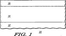
図中の各要素は簡単明瞭であるように図示されており、必ずしも縮尺通りに描かれていない点は当業者であれば理解するであろう。例えば、図中の一部の要素の寸法は、本発明の開示の実施形態の理解向上を助けるために他の要素に対して強調している場合がある。
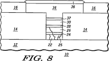
34 半導体デバイス層
36 歪み材料層
40 ゲート誘電体材料
44 拡大注入領域
46 側壁スペーサ
48 ソース/ドレイン領域
Claims (4)
- 第1格子定数を有する第1緩和半導体材料を含む基板と、
前記基板を覆い、前記第1格子定数とは異なる第2格子定数を有する第2緩和半導体材料を含む半導体デバイス層と、
前記基板と前記半導体デバイス層との間に介在された誘電体層と、
を備え、
前記誘電体層が、前記第1格子定数と前記第2格子定数との間で遷移するように前記誘電体層内に配置されたプログラムされた遷移帯を有し、前記プログラムされた遷移帯が複数層を含み、前記複数層の隣接する層が異なる格子定数を有し、該隣接する層の1つが欠陥を形成するのに必要な第1限界厚さを超える第1厚さを有し、且つ前記隣接する層の他のものが第2限界厚さを超えない第2厚さを有しており、前記複数層の各隣接する層が、前記プログラムされた遷移帯内の欠陥を促進して前記プログラムされた遷移帯の縁部に移行させる境界面を形成することを特徴とする半導体構造体。 - 前記半導体デバイス層を覆い、欠陥を最小化して歪みを維持するために限界厚さ未満の厚さを有する歪み材料層を更に備える請求項1に記載の半導体構造体。
- 半導体デバイス構造の形成方法であって、
第1格子定数を有する第1緩和材料から構成された基板手段を形成する段階と、
前記基板手段を覆い、前記第1格子定数を有する前記第1緩和材料から異なる第2格子定数の材料に遷移するようにプログラムされた遷移帯を定める開口部を有する誘電体層手段を形成する段階と、
欠陥を形成して歪みを除去するような材料組成の限界厚さを超える厚さを有する層と、歪みを生じる材料組成の限界厚さを超えない厚さを有する層とを交互に形成し、欠陥を促進して前記プログラムされた遷移帯の縁部に移行させる境界面を形成するために、隣接する任意の層とは異なる格子定数を各々が含む複数層を備え、最上層が欠陥が無いようにする前記プログラムされた遷移帯を形成する段階と、
少なくとも前記プログラムされた遷移帯を覆い、前記異なる格子定数である第2格子定数を有する第2緩和材料から構成される半導体デバイス層手段を形成する段階と、
を含み、
前記プログラムされた遷移帯は、前記基板手段及び前記半導体デバイス層手段間の格子定数の差異によって生じる歪が完全に除去され、且つ、全ての欠陥が前記プログラムされた遷移帯内で終端するように形成されていることを特徴とする半導体デバイスを形成する方法。 - 半導体デバイスを形成する方法であって、
第1格子定数を有する第1緩和材料からなる基板手段を形成する段階と、
前記基板手段の上に横たわる誘電層手段を形成する段階であって、該誘電層手段が、第1格子定数を備えた第1の関連する材料から、異なる第2格子定数材料まで遷移するようにプログラムされた遷移帯を画定するための開口部を備え、
複数層を備えて前記プログラムされた遷移帯を形成する段階と、
を含み、
前記複数層の複数層の隣接する層が異なる格子定数を有し、該隣接する層の各々の1つが欠陥を形成するのに必要な限界厚さを超える第1厚さを有し且つ前記隣接する層の各々の他のものが欠陥を形成するのに要求される限界厚さを超えない第2厚さを有しており、前記複数層の各隣接する層が、前記プログラムされた遷移帯内の欠陥を促進して前記プログラムされた遷移帯の縁部に移行させる境界面を形成し、前記プログラムされた遷移帯の最上層が欠陥が無いようにする段階と、
を含む方法。
Applications Claiming Priority (3)
| Application Number | Priority Date | Filing Date | Title |
|---|---|---|---|
| US10/677,844 | 2003-10-02 | ||
| US10/677,844 US6831350B1 (en) | 2003-10-02 | 2003-10-02 | Semiconductor structure with different lattice constant materials and method for forming the same |
| PCT/US2004/031516 WO2005034230A1 (en) | 2003-10-02 | 2004-09-27 | Semiconductor structure with different lattice constant materials and method for forming the same |
Publications (3)
| Publication Number | Publication Date |
|---|---|
| JP2007507896A JP2007507896A (ja) | 2007-03-29 |
| JP2007507896A5 JP2007507896A5 (ja) | 2007-11-15 |
| JP4901476B2 true JP4901476B2 (ja) | 2012-03-21 |
Family
ID=33490980
Family Applications (1)
| Application Number | Title | Priority Date | Filing Date |
|---|---|---|---|
| JP2006533987A Expired - Fee Related JP4901476B2 (ja) | 2003-10-02 | 2004-09-27 | 格子定数の異なる材料を用いる半導体構造及び同構造の形成方法 |
Country Status (6)
| Country | Link |
|---|---|
| US (1) | US6831350B1 (ja) |
| JP (1) | JP4901476B2 (ja) |
| KR (1) | KR101115091B1 (ja) |
| CN (1) | CN100487876C (ja) |
| TW (1) | TWI356491B (ja) |
| WO (1) | WO2005034230A1 (ja) |
Families Citing this family (34)
| Publication number | Priority date | Publication date | Assignee | Title |
|---|---|---|---|---|
| US6919258B2 (en) * | 2003-10-02 | 2005-07-19 | Freescale Semiconductor, Inc. | Semiconductor device incorporating a defect controlled strained channel structure and method of making the same |
| DE102004053307B4 (de) * | 2004-11-04 | 2010-01-07 | Siltronic Ag | Mehrschichtenstruktur umfassend ein Substrat und eine darauf heteroepitaktisch abgeschiedene Schicht aus Silicium und Germanium und ein Verfahren zu deren Herstellung |
| US8324660B2 (en) | 2005-05-17 | 2012-12-04 | Taiwan Semiconductor Manufacturing Company, Ltd. | Lattice-mismatched semiconductor structures with reduced dislocation defect densities and related methods for device fabrication |
| US9153645B2 (en) | 2005-05-17 | 2015-10-06 | Taiwan Semiconductor Manufacturing Company, Ltd. | Lattice-mismatched semiconductor structures with reduced dislocation defect densities and related methods for device fabrication |
| FR2888400B1 (fr) * | 2005-07-08 | 2007-10-19 | Soitec Silicon On Insulator | Procede de prelevement de couche |
| US7524707B2 (en) | 2005-08-23 | 2009-04-28 | Freescale Semiconductor, Inc. | Modified hybrid orientation technology |
| US7947546B2 (en) | 2005-10-31 | 2011-05-24 | Chartered Semiconductor Manufacturing, Ltd. | Implant damage control by in-situ C doping during SiGe epitaxy for device applications |
| US7479422B2 (en) * | 2006-03-10 | 2009-01-20 | Freescale Semiconductor, Inc. | Semiconductor device with stressors and method therefor |
| US7777250B2 (en) | 2006-03-24 | 2010-08-17 | Taiwan Semiconductor Manufacturing Company, Ltd. | Lattice-mismatched semiconductor structures and related methods for device fabrication |
| US7700420B2 (en) * | 2006-04-12 | 2010-04-20 | Freescale Semiconductor, Inc. | Integrated circuit with different channel materials for P and N channel transistors and method therefor |
| EP2062290B1 (en) | 2006-09-07 | 2019-08-28 | Taiwan Semiconductor Manufacturing Company, Ltd. | Defect reduction using aspect ratio trapping |
| US7875958B2 (en) | 2006-09-27 | 2011-01-25 | Taiwan Semiconductor Manufacturing Company, Ltd. | Quantum tunneling devices and circuits with lattice-mismatched semiconductor structures |
| US8502263B2 (en) | 2006-10-19 | 2013-08-06 | Taiwan Semiconductor Manufacturing Company, Ltd. | Light-emitter-based devices with lattice-mismatched semiconductor structures |
| WO2008124154A2 (en) | 2007-04-09 | 2008-10-16 | Amberwave Systems Corporation | Photovoltaics on silicon |
| US8304805B2 (en) | 2009-01-09 | 2012-11-06 | Taiwan Semiconductor Manufacturing Company, Ltd. | Semiconductor diodes fabricated by aspect ratio trapping with coalesced films |
| US7825328B2 (en) | 2007-04-09 | 2010-11-02 | Taiwan Semiconductor Manufacturing Company, Ltd. | Nitride-based multi-junction solar cell modules and methods for making the same |
| US8237151B2 (en) * | 2009-01-09 | 2012-08-07 | Taiwan Semiconductor Manufacturing Company, Ltd. | Diode-based devices and methods for making the same |
| US8329541B2 (en) | 2007-06-15 | 2012-12-11 | Taiwan Semiconductor Manufacturing Company, Ltd. | InP-based transistor fabrication |
| DE112008002387B4 (de) | 2007-09-07 | 2022-04-07 | Taiwan Semiconductor Manufacturing Co., Ltd. | Struktur einer Mehrfachübergangs-Solarzelle, Verfahren zur Bildung einer photonischenVorrichtung, Photovoltaische Mehrfachübergangs-Zelle und Photovoltaische Mehrfachübergangs-Zellenvorrichtung, |
| US8183667B2 (en) | 2008-06-03 | 2012-05-22 | Taiwan Semiconductor Manufacturing Co., Ltd. | Epitaxial growth of crystalline material |
| US8274097B2 (en) | 2008-07-01 | 2012-09-25 | Taiwan Semiconductor Manufacturing Company, Ltd. | Reduction of edge effects from aspect ratio trapping |
| US8981427B2 (en) | 2008-07-15 | 2015-03-17 | Taiwan Semiconductor Manufacturing Company, Ltd. | Polishing of small composite semiconductor materials |
| US20100072515A1 (en) | 2008-09-19 | 2010-03-25 | Amberwave Systems Corporation | Fabrication and structures of crystalline material |
| JP5416212B2 (ja) | 2008-09-19 | 2014-02-12 | 台湾積體電路製造股▲ふん▼有限公司 | エピタキシャル層の成長によるデバイス形成 |
| US8253211B2 (en) | 2008-09-24 | 2012-08-28 | Taiwan Semiconductor Manufacturing Company, Ltd. | Semiconductor sensor structures with reduced dislocation defect densities |
| CN102379046B (zh) | 2009-04-02 | 2015-06-17 | 台湾积体电路制造股份有限公司 | 从晶体材料的非极性平面形成的器件及其制作方法 |
| EP2423951B1 (en) * | 2010-08-05 | 2016-07-20 | Imec | Antiphase domain boundary-free III-V compound semiconductor material on semiconductor substrate and method for manufacturing thereof |
| US9099421B2 (en) * | 2012-10-31 | 2015-08-04 | Taiwan Semiconductor Manufacturing Company Limited | Surface profile for semiconductor region |
| KR102176646B1 (ko) * | 2014-03-28 | 2020-11-09 | 인텔 코포레이션 | 트랜지스터들에서의 변형 보상 |
| US10170549B2 (en) | 2014-10-21 | 2019-01-01 | Samsung Electronics Co., Ltd. | Strained stacked nanosheet FETs and/or quantum well stacked nanosheet |
| US9735010B1 (en) | 2016-05-27 | 2017-08-15 | International Business Machines Corporation | Fabrication of semiconductor fin structures |
| US10249492B2 (en) | 2016-05-27 | 2019-04-02 | International Business Machines Corporation | Fabrication of compound semiconductor structures |
| CN108807279B (zh) * | 2018-06-25 | 2021-01-22 | 中国科学院微电子研究所 | 半导体结构与其制作方法 |
| TWI698912B (zh) * | 2018-09-03 | 2020-07-11 | 環球晶圓股份有限公司 | 磊晶基板及其製造方法 |
Family Cites Families (35)
| Publication number | Priority date | Publication date | Assignee | Title |
|---|---|---|---|---|
| US4522662A (en) | 1983-08-12 | 1985-06-11 | Hewlett-Packard Company | CVD lateral epitaxial growth of silicon over insulators |
| US4557794A (en) | 1984-05-07 | 1985-12-10 | Rca Corporation | Method for forming a void-free monocrystalline epitaxial layer on a mask |
| US4619033A (en) | 1985-05-10 | 1986-10-28 | Rca Corporation | Fabricating of a CMOS FET with reduced latchup susceptibility |
| US4891092A (en) | 1986-01-13 | 1990-01-02 | General Electric Company | Method for making a silicon-on-insulator substrate |
| US4755481A (en) | 1986-05-15 | 1988-07-05 | General Electric Company | Method of making a silicon-on-insulator transistor |
| US4760036A (en) | 1987-06-15 | 1988-07-26 | Delco Electronics Corporation | Process for growing silicon-on-insulator wafers using lateral epitaxial growth with seed window oxidation |
| FR2629636B1 (fr) | 1988-04-05 | 1990-11-16 | Thomson Csf | Procede de realisation d'une alternance de couches de materiau semiconducteur monocristallin et de couches de materiau isolant |
| EP0391081A3 (en) | 1989-04-06 | 1991-08-07 | International Business Machines Corporation | Fabrication and structure of semiconductor-on-insulator islands |
| JPH02302044A (ja) | 1989-05-16 | 1990-12-14 | Fujitsu Ltd | 半導体装置の製造方法 |
| US5202284A (en) | 1989-12-01 | 1993-04-13 | Hewlett-Packard Company | Selective and non-selective deposition of Si1-x Gex on a Si subsrate that is partially masked with SiO2 |
| US5273921A (en) | 1991-12-27 | 1993-12-28 | Purdue Research Foundation | Methods for fabricating a dual-gated semiconductor-on-insulator field effect transistor |
| US5445107A (en) | 1993-11-22 | 1995-08-29 | Motorola, Inc. | Semiconductor device and method of formation |
| US5963817A (en) * | 1997-10-16 | 1999-10-05 | International Business Machines Corporation | Bulk and strained silicon on insulator using local selective oxidation |
| JP3403076B2 (ja) * | 1998-06-30 | 2003-05-06 | 株式会社東芝 | 半導体装置及びその製造方法 |
| US6392253B1 (en) | 1998-08-10 | 2002-05-21 | Arjun J. Saxena | Semiconductor device with single crystal films grown on arrayed nucleation sites on amorphous and/or non-single crystal surfaces |
| US6110278A (en) | 1998-08-10 | 2000-08-29 | Saxena; Arjun N. | Methods for and products of growth of single-crystal on arrayed nucleation sites (SCANS) defined in nucleation unfriendly substrates |
| US6350993B1 (en) | 1999-03-12 | 2002-02-26 | International Business Machines Corporation | High speed composite p-channel Si/SiGe heterostructure for field effect devices |
| US6214653B1 (en) | 1999-06-04 | 2001-04-10 | International Business Machines Corporation | Method for fabricating complementary metal oxide semiconductor (CMOS) devices on a mixed bulk and silicon-on-insulator (SOI) substrate |
| US6261878B1 (en) | 1999-06-21 | 2001-07-17 | Intel Corporation | Integrated circuit with dynamic threshold voltage |
| US6228691B1 (en) | 1999-06-30 | 2001-05-08 | Intel Corp. | Silicon-on-insulator devices and method for producing the same |
| US6326272B1 (en) | 1999-11-18 | 2001-12-04 | Chartered Semiconductor Manufacturing Ltd. | Method for forming self-aligned elevated transistor |
| US6429099B1 (en) | 2000-01-05 | 2002-08-06 | International Business Machines Corporation | Implementing contacts for bodies of semiconductor-on-insulator transistors |
| US6362071B1 (en) | 2000-04-05 | 2002-03-26 | Motorola, Inc. | Method for forming a semiconductor device with an opening in a dielectric layer |
| EP1399970A2 (en) | 2000-12-04 | 2004-03-24 | Amberwave Systems Corporation | Cmos inverter circuits utilizing strained silicon surface channel mosfets |
| US6830976B2 (en) | 2001-03-02 | 2004-12-14 | Amberwave Systems Corproation | Relaxed silicon germanium platform for high speed CMOS electronics and high speed analog circuits |
| US6703688B1 (en) * | 2001-03-02 | 2004-03-09 | Amberwave Systems Corporation | Relaxed silicon germanium platform for high speed CMOS electronics and high speed analog circuits |
| US6900103B2 (en) | 2001-03-02 | 2005-05-31 | Amberwave Systems Corporation | Relaxed silicon germanium platform for high speed CMOS electronics and high speed analog circuits |
| EP1364411A1 (en) * | 2001-03-02 | 2003-11-26 | Amberwave Systems Corporation | Relaxed silicon germanium platform for high speed cmos electronics and high speed analog circuits |
| EP1399974A1 (en) | 2001-06-21 | 2004-03-24 | Massachusetts Institute Of Technology | Mosfets with strained semiconductor layers |
| US6730551B2 (en) | 2001-08-06 | 2004-05-04 | Massachusetts Institute Of Technology | Formation of planar strained layers |
| US6974735B2 (en) | 2001-08-09 | 2005-12-13 | Amberwave Systems Corporation | Dual layer Semiconductor Devices |
| EP1428262A2 (en) | 2001-09-21 | 2004-06-16 | Amberwave Systems Corporation | Semiconductor structures employing strained material layers with defined impurity gradients and methods for fabricating same |
| US6600170B1 (en) * | 2001-12-17 | 2003-07-29 | Advanced Micro Devices, Inc. | CMOS with strained silicon channel NMOS and silicon germanium channel PMOS |
| US6492216B1 (en) | 2002-02-07 | 2002-12-10 | Taiwan Semiconductor Manufacturing Company | Method of forming a transistor with a strained channel |
| JP2004342819A (ja) * | 2003-05-15 | 2004-12-02 | Toshiba Ceramics Co Ltd | 半導体基板およびその製造方法 |
-
2003
- 2003-10-02 US US10/677,844 patent/US6831350B1/en not_active Expired - Lifetime
-
2004
- 2004-09-27 CN CNB2004800265755A patent/CN100487876C/zh not_active Expired - Fee Related
- 2004-09-27 KR KR1020067006304A patent/KR101115091B1/ko not_active IP Right Cessation
- 2004-09-27 WO PCT/US2004/031516 patent/WO2005034230A1/en active Application Filing
- 2004-09-27 JP JP2006533987A patent/JP4901476B2/ja not_active Expired - Fee Related
- 2004-10-01 TW TW093129747A patent/TWI356491B/zh not_active IP Right Cessation
Also Published As
| Publication number | Publication date |
|---|---|
| WO2005034230A1 (en) | 2005-04-14 |
| CN1853260A (zh) | 2006-10-25 |
| US6831350B1 (en) | 2004-12-14 |
| KR20060090242A (ko) | 2006-08-10 |
| JP2007507896A (ja) | 2007-03-29 |
| CN100487876C (zh) | 2009-05-13 |
| KR101115091B1 (ko) | 2012-03-13 |
| TW200524155A (en) | 2005-07-16 |
| TWI356491B (en) | 2012-01-11 |
Similar Documents
| Publication | Publication Date | Title |
|---|---|---|
| JP4901476B2 (ja) | 格子定数の異なる材料を用いる半導体構造及び同構造の形成方法 | |
| KR102110858B1 (ko) | 결함 이동 및 격자 불일치된 에피택셜 막 | |
| CN106328538B (zh) | 自对准硅锗鳍式fet | |
| US7791064B2 (en) | Semiconductor device and fabrication method thereof | |
| KR101354844B1 (ko) | 반도체 장치 및 그의 제조 방법 | |
| US20050205936A1 (en) | Semiconductor device incorporating a defect controlled strained channel structure and method of making the same | |
| US11374106B2 (en) | Method of making heteroepitaxial structures and device formed by the method | |
| KR20120089354A (ko) | 양자 웰 트랜지스터에 접촉부를 형성하는 기술 | |
| WO2014099036A1 (en) | Expitaxial film on nanoscale structure | |
| TW201635517A (zh) | 具有替代通道材料之電性絕緣鰭片結構及其製法 | |
| US20170062426A1 (en) | Co-integration of tensile silicon and compressive silicon germanium | |
| KR20150000386A (ko) | 응력 변형된 반도체 구조물 형성 방법 | |
| JP2007506290A (ja) | 絶縁構造部上の半導体チャンネル | |
| JP4888385B2 (ja) | 半導体装置及びその製造方法 | |
| US9337281B2 (en) | Planar semiconductor growth on III-V material | |
| JPH07193233A (ja) | ゲート壁側壁なしトランジスタの製造方法 | |
| CN113471138A (zh) | 半导体基底的制备方法及半导体器件 | |
| US10600890B2 (en) | Contact to metal gate isolation structure | |
| JP4221928B2 (ja) | 半導体基板及び電界効果型トランジスタ並びにこれらの製造方法 | |
| US20120228628A1 (en) | Semiconductor device and method of fabricating the same | |
| EP2693462B1 (en) | Method for manufacturing semiconductor devices |
Legal Events
| Date | Code | Title | Description |
|---|---|---|---|
| A521 | Request for written amendment filed |
Free format text: JAPANESE INTERMEDIATE CODE: A523 Effective date: 20070926 |
|
| A621 | Written request for application examination |
Free format text: JAPANESE INTERMEDIATE CODE: A621 Effective date: 20070926 |
|
| A131 | Notification of reasons for refusal |
Free format text: JAPANESE INTERMEDIATE CODE: A131 Effective date: 20110620 |
|
| RD04 | Notification of resignation of power of attorney |
Free format text: JAPANESE INTERMEDIATE CODE: A7424 Effective date: 20110912 |
|
| A521 | Request for written amendment filed |
Free format text: JAPANESE INTERMEDIATE CODE: A523 Effective date: 20110920 |
|
| TRDD | Decision of grant or rejection written | ||
| A01 | Written decision to grant a patent or to grant a registration (utility model) |
Free format text: JAPANESE INTERMEDIATE CODE: A01 Effective date: 20111130 |
|
| A01 | Written decision to grant a patent or to grant a registration (utility model) |
Free format text: JAPANESE INTERMEDIATE CODE: A01 |
|
| A61 | First payment of annual fees (during grant procedure) |
Free format text: JAPANESE INTERMEDIATE CODE: A61 Effective date: 20111227 |
|
| R150 | Certificate of patent or registration of utility model |
Ref document number: 4901476 Country of ref document: JP Free format text: JAPANESE INTERMEDIATE CODE: R150 Free format text: JAPANESE INTERMEDIATE CODE: R150 |
|
| FPAY | Renewal fee payment (event date is renewal date of database) |
Free format text: PAYMENT UNTIL: 20150113 Year of fee payment: 3 |
|
| R250 | Receipt of annual fees |
Free format text: JAPANESE INTERMEDIATE CODE: R250 |
|
| R250 | Receipt of annual fees |
Free format text: JAPANESE INTERMEDIATE CODE: R250 |
|
| R250 | Receipt of annual fees |
Free format text: JAPANESE INTERMEDIATE CODE: R250 |
|
| S533 | Written request for registration of change of name |
Free format text: JAPANESE INTERMEDIATE CODE: R313533 |
|
| R350 | Written notification of registration of transfer |
Free format text: JAPANESE INTERMEDIATE CODE: R350 |
|
| R250 | Receipt of annual fees |
Free format text: JAPANESE INTERMEDIATE CODE: R250 |
|
| LAPS | Cancellation because of no payment of annual fees |