JP4898024B2 - Manufacturing method of semiconductor device - Google Patents
Manufacturing method of semiconductor device Download PDFInfo
- Publication number
- JP4898024B2 JP4898024B2 JP2001188050A JP2001188050A JP4898024B2 JP 4898024 B2 JP4898024 B2 JP 4898024B2 JP 2001188050 A JP2001188050 A JP 2001188050A JP 2001188050 A JP2001188050 A JP 2001188050A JP 4898024 B2 JP4898024 B2 JP 4898024B2
- Authority
- JP
- Japan
- Prior art keywords
- polycrystalline silicon
- insulating film
- film
- semiconductor device
- impurity
- Prior art date
- Legal status (The legal status is an assumption and is not a legal conclusion. Google has not performed a legal analysis and makes no representation as to the accuracy of the status listed.)
- Expired - Fee Related
Links
Images


Classifications
-
- H—ELECTRICITY
- H10—SEMICONDUCTOR DEVICES; ELECTRIC SOLID-STATE DEVICES NOT OTHERWISE PROVIDED FOR
- H10D—INORGANIC ELECTRIC SEMICONDUCTOR DEVICES
- H10D1/00—Resistors, capacitors or inductors
- H10D1/40—Resistors
- H10D1/47—Resistors having no potential barriers
-
- H—ELECTRICITY
- H10—SEMICONDUCTOR DEVICES; ELECTRIC SOLID-STATE DEVICES NOT OTHERWISE PROVIDED FOR
- H10D—INORGANIC ELECTRIC SEMICONDUCTOR DEVICES
- H10D84/00—Integrated devices formed in or on semiconductor substrates that comprise only semiconducting layers, e.g. on Si wafers or on GaAs-on-Si wafers
- H10D84/01—Manufacture or treatment
- H10D84/0123—Integrating together multiple components covered by H10D12/00 or H10D30/00, e.g. integrating multiple IGBTs
- H10D84/0126—Integrating together multiple components covered by H10D12/00 or H10D30/00, e.g. integrating multiple IGBTs the components including insulated gates, e.g. IGFETs
- H10D84/0165—Integrating together multiple components covered by H10D12/00 or H10D30/00, e.g. integrating multiple IGBTs the components including insulated gates, e.g. IGFETs the components including complementary IGFETs, e.g. CMOS devices
- H10D84/0172—Manufacturing their gate conductors
- H10D84/0174—Manufacturing their gate conductors the gate conductors being silicided
-
- H—ELECTRICITY
- H10—SEMICONDUCTOR DEVICES; ELECTRIC SOLID-STATE DEVICES NOT OTHERWISE PROVIDED FOR
- H10D—INORGANIC ELECTRIC SEMICONDUCTOR DEVICES
- H10D84/00—Integrated devices formed in or on semiconductor substrates that comprise only semiconducting layers, e.g. on Si wafers or on GaAs-on-Si wafers
- H10D84/01—Manufacture or treatment
- H10D84/0123—Integrating together multiple components covered by H10D12/00 or H10D30/00, e.g. integrating multiple IGBTs
- H10D84/0126—Integrating together multiple components covered by H10D12/00 or H10D30/00, e.g. integrating multiple IGBTs the components including insulated gates, e.g. IGFETs
- H10D84/0165—Integrating together multiple components covered by H10D12/00 or H10D30/00, e.g. integrating multiple IGBTs the components including insulated gates, e.g. IGFETs the components including complementary IGFETs, e.g. CMOS devices
- H10D84/0172—Manufacturing their gate conductors
- H10D84/0177—Manufacturing their gate conductors the gate conductors having different materials or different implants
-
- H—ELECTRICITY
- H10—SEMICONDUCTOR DEVICES; ELECTRIC SOLID-STATE DEVICES NOT OTHERWISE PROVIDED FOR
- H10D—INORGANIC ELECTRIC SEMICONDUCTOR DEVICES
- H10D84/00—Integrated devices formed in or on semiconductor substrates that comprise only semiconducting layers, e.g. on Si wafers or on GaAs-on-Si wafers
- H10D84/01—Manufacture or treatment
- H10D84/02—Manufacture or treatment characterised by using material-based technologies
- H10D84/03—Manufacture or treatment characterised by using material-based technologies using Group IV technology, e.g. silicon technology or silicon-carbide [SiC] technology
- H10D84/038—Manufacture or treatment characterised by using material-based technologies using Group IV technology, e.g. silicon technology or silicon-carbide [SiC] technology using silicon technology, e.g. SiGe
-
- H—ELECTRICITY
- H10—SEMICONDUCTOR DEVICES; ELECTRIC SOLID-STATE DEVICES NOT OTHERWISE PROVIDED FOR
- H10D—INORGANIC ELECTRIC SEMICONDUCTOR DEVICES
- H10D84/00—Integrated devices formed in or on semiconductor substrates that comprise only semiconducting layers, e.g. on Si wafers or on GaAs-on-Si wafers
- H10D84/80—Integrated devices formed in or on semiconductor substrates that comprise only semiconducting layers, e.g. on Si wafers or on GaAs-on-Si wafers characterised by the integration of at least one component covered by groups H10D12/00 or H10D30/00, e.g. integration of IGFETs
- H10D84/811—Combinations of field-effect devices and one or more diodes, capacitors or resistors
- H10D84/817—Combinations of field-effect devices and resistors only
Landscapes
- Metal-Oxide And Bipolar Metal-Oxide Semiconductor Integrated Circuits (AREA)
- Semiconductor Integrated Circuits (AREA)
Description
【0001】
【発明の属する技術分野】
本発明は抵抗回路を有する相補型MOS半導体装置において低電圧動作、低消費電力および高駆動能力が要求される半導体装置、特に電圧検出器(Voltage Detector、以後VDと表記)や定電圧レギュレータ(Voltage Regulator、以後VRと表記)やスイッチングレギュレータ(Switching Regulator、以後SWRと表記など)などのパワーマネージメント半導体装置やオペアンプ、コンパレータなどのアナログ半導体装置の製造方法に関する。
【0002】
【従来の技術】
従来多結晶シリコンなどの抵抗体を使用した抵抗回路を有する相補型MOS半導体装置は数多く使用されている。図14は従来の抵抗回路を備えた半導体装置の構造の一実施例を示したものである。P型半導体基板に形成されたゲート電極がN+型の多結晶シリコンからなるNチャネル型MOSトランジスタ(以後NMOSと表記)と、Nウェル領域に形成されたゲート電極がやはりN+型の多結晶シリコンからなるPチャネル型MOSトランジスタ(以後PMOSと表記)とからなる相補型MOS構造(Complementary MOS、以後CMOS表記)と、フィールド絶縁膜上に形成されている電圧を分圧するための分圧回路もしくは時定数を設定するCR回路などに用いられる抵抗体とから構成されている。
【0003】
【発明が解決しようとする課題】
この抵抗回路を有する相補型MOS(CMOS)半導体装置において、ゲート電極の極性はその製造の容易さ、安定性より、N+型多結晶シリコンがよく用いられている。この場合ゲート電極と半導体基板(ウェル)の仕事関数の関係よりNMOSトランジスタは表面チャネル型となるが、PMOSトランジスタの場合、やはりゲート電極と半導体基板の仕事関数の関係によりしきい値電圧は約-1Vとなる。そのためしきい値電圧を低下させるために不純物注入を行うと、表面より少し基板内部にチャネル形成する埋め込みチャネルとなってしまう。埋め込みチャネルは基板内部をキャリアが通過するため移動度が大きいという利点があるが、しきい値電圧を下げるとサブスレッショルド特性は極めて劣化し、リーク電流が増加する。そのためNMOSトランジスタに比べPMOSトランジスタは低電圧化、短チャネル化が困難である。
【0004】
またNMOSトランジスタ、PMOSトランジスタともに低電圧化が可能となる構造として、ゲート電極の極性をトランジスタの極性と等しくする同極ゲート構造というものがある。この構造はNMOSトランジスタのゲート電極にはN+型多結晶シリコン、PMOSトランジスタにはP+型多結晶シリコンを用いるためどちらも表面チャネル型となりリーク電流を抑えることができ低電圧化が可能となる。しかしながらゲート電極の極性を別々にすることによる製造工程数が増加し製造コストや製造工期の増大を招き、さらに最も基本的な回路要素であるインバータ回路においては通常は、面積効率の向上のためにNMOSトランジスタとPMOSトランジスタのゲート電極はメタルを介しての結線を避け平面的にNMOSトランジスタからPMOSトランジスタまで連続な1個の多結晶シリコンないしは多結晶シリコンと高融点金属シリサイドとの積層からなるポリサイド構造によりレイアウトされるが、図4に示すような多結晶シリコン単層から形成される場合にはその多結晶シリコン中のPN接合のインピーダンスが高く実用的でないこと、図5に示すようなポリサイド構造の場合にはN型とP型の不純物は工程における熱処理中に高融点金属シリサイド中を高速でお互いに逆導電型のゲート電極へ拡散し、その結果として仕事関数が変化してしきい値電圧が安定しないなどの、コスト面や特性面において問題を有している。
【0005】
【課題を解決するための手段】
上記課題を解決するために、本発明は次の手段を用いた。
【0006】
(1)半導体基板上に熱酸化による素子分離絶縁膜を形成する工程と、熱酸化によるゲート絶縁膜を形成する工程と、ゲート絶縁膜上に500Å〜2500Åの第1の多結晶シリコン膜を堆積する工程と、第1の多結晶シリコン膜に不純物濃度が1×1018atoms/cm3以上となるように不純物をドーピングを行い第1の多結晶シリコン膜の導電型をP型する工程と、第1のP型多結晶シリコン上に500Å〜2500Åからなる高融点金属シリサイドを堆積する工程と、高融点金属シリサイド上に500Å〜3000Åからなる絶縁膜を堆積する工程と、第1のP型多結晶シリコンと高融点金属シリサイドと絶縁膜をエッチングし積層のポリサイドゲート電極を形成する工程と、第1の導電型のMOSトランジスタの低濃度拡散領域に第1の導電型の不純物を1×1016〜1×1018atoms/cm3ドーピングする工程と、第2の導電型のMOSトランジスタの低濃度拡散領域に第2の導電型の不純物を1×1016〜1×1018atoms/cm3ドーピングする工程と、ポリサイドゲート電極上にポリサイドゲート電極と同程度の膜厚の絶縁膜を堆積する工程と、異方性ドライエッチで絶縁膜をエッチングしポリサイドゲート電極側壁にサイドスペーサーを形成する工程と、素子分離絶縁膜上に500Å〜2500Åからなる第2の多結晶シリコン膜を堆積する工程と、第2の多結晶シリコン膜の全域ないしは第2の多結晶シリコン膜の第1の領域に第2の導電型の不純物を1×1014〜9×1018atoms/cm3ドーピングする工程と、第2の多結晶シリコン膜の第2の領域に第1の導電型の不純物を1×1014〜9×1018atoms/cm3ドーピングする工程と、第2の多結晶シリコン膜をエッチングし第2の多結晶シリコン膜の抵抗体を形成する工程と、第2の多結晶シリコン膜の第1の領域の一部ないし全域に1×1019atoms/cm3以上の第1の導電型の不純物をドーピングする工程と、第2の多結晶シリコン膜の第2の領域の一部ないし全域に1×1019atoms/cm3以上の第2の導電型の不純物をドーピングする工程と、半導体基板上に中間絶縁膜を形成する工程と、半導体基板上の中間絶縁膜にコンタクト孔を形成する工程と、コンタクト孔に金属配線を設けることからなる半導体装置の製造方法とした。
【0007】
(2)第1の多結晶シリコン膜への不純物導入法がボロンのイオン注入であることを特徴とする半導体装置の製造方法とした。
【0008】
(3)第1の多結晶シリコン膜への不純物導入法が、BF2のイオン注入であることを特徴とする半導体装置の製造方法とした。
【0009】
(4)第1の多結晶シリコン膜への不純物導入法が、第1の多結晶シリコン膜の堆積時に不純物を同時に混入しながら堆積するDoped−CVD法であることを特徴とする半導体装置の製造方法とした。
【0010】
(5)高融点金属シリサイド上に堆積した絶縁膜が酸化膜で構成されていることを特徴とする半導体装置の製造方法とした。
【0011】
(6)高融点金属シリサイド上に堆積した絶縁膜が酸化膜である時、ポリサイドゲート電極側壁に形成するサイドスペーサーの材料となる絶縁膜が窒化膜であることを特徴とする半導体装置の製造方法とした。
【0012】
(7)高融点金属シリサイド上に堆積した絶縁膜が窒化膜で構成されていることを特徴とする半導体装置の製造方法とした。
【0013】
(8)高融点金属シリサイド上に堆積した絶縁膜が窒化膜である時、ポリサイドゲート電極側壁に形成するサイドスペーサーの材料となる絶縁膜が酸化膜であることを特徴とする半導体装置の製造方法とした。
【0014】
(9)高融点金属シリサイド上に堆積した絶縁膜が酸化膜及び窒化膜及び別層の酸化膜の積層構造で構成されていることを特徴とする半導体装置の製造方法とした。
【0015】
(10)高融点金属シリサイド上に堆積した絶縁膜が積層構造で最上層が酸化膜である時、ポリサイドゲート電極側壁に形成するサイドスペーサーの材料となる絶縁膜が窒化膜であることを特徴とする半導体装置の製造方法とした。
【0016】
(11)第2の多結晶シリコン膜の第1の領域の一部及び全域への1×10¹⁹atoms/cm3以上の第1の導電型の不純物ドーピングが第1の導電型のMOSトランジスタの拡散領域ドーピングと同時であり、第2の多結晶シリコン膜の第2の領域の一部及び全域への1×1019atoms/cm3以上の第2の導電型の不純物ドーピングが第2の導電型のMOSトランジスタの拡散領域ドーピングと同時であることを特徴とする半導体装置の製造方法とした。
【0017】
【発明の実施の形態】
以下、本発明の実施例を図面を用いて詳細に説明する。
図1は本発明の抵抗回路を有するCMOS半導体装置の一実施例を示す断面図である。
【0018】
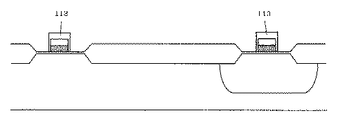
本実施例では、P型シリコン半導体基板101中に基板とは逆導電型のN型ウェル拡散層領域102が形成されている。さらにシリコン半導体基板101中には基板とは逆導電型の不純物拡散層によるN型MOSトランジスタ114、N型ウェル拡散層領域102にはウェルと逆導電型の不純物拡散層によるP型MOSトランジスタ115が形成されている。そしてゲート絶縁膜105、ゲート電極となるP+型多結晶シリコン107と高融点金属シリサイド112の積層ポリサイド構造で、おのおののトランジスタが構成されている。そしてゲート電極のマスク材として酸化膜絶縁膜113をゲート電極の上に堆積させている。ここでゲート電極のマスク材として窒化膜を用いても構わない。また、ここではP型シリコン半導体基板を用いたが、N型シリコン基板上にP型ウェル拡散層を形成し、そこにCMOS半導体装置を構成しても構わない。
【0019】
また本実施例において、フィールド絶縁膜106上に第1導電型であるN型の第2の多結晶シリコン抵抗体116と、第2導電型であるP型の第2の多結晶シリコン抵抗体117が形成されているが、CMOSのゲート電極の一部である多結晶シリコン107と多結晶シリコン抵抗体116、117は別工程で形成され、膜厚も異なっており、多結晶シリコン抵抗体の方がゲート電極より薄く形成されている。たとえばゲート電極膜厚は2000Åから6000Å程度の膜厚であるのに対し、抵抗体の膜厚は500Åから2500Åで形成される。これは多結晶シリコン抵抗体においては膜厚は薄い方がシート抵抗値を高く設定でき,また温度特性も良くなるため、より精度を向上させることができる。
【0020】
N型多結晶シリコン抵抗体116には高抵抗領域110と抵抗体両端に配線材と十分なコンタクトを取ることの出来る高濃度不純物領域108を有している。そして高抵抗領域110の不純物濃度をイオン注入で制御し、所望の抵抗値を有する抵抗体を形成する。同様にP型多結晶シリコン抵抗体117にも高抵抗領域111と高濃度不純物領域109を有し、高抵抗領域の不純物濃度により抵抗値を設定する。
【0021】
例えば、シート抵抗値はその抵抗の用途にもよるが通常の分圧回路においては数kΩ/□から数十kΩ/□の範囲で使われる。この時の不純物はP−抵抗体117においてはボロンないしBF2を用い1×1014〜9×1018atoms/cm3程度の濃度であり、N−抵抗体116においてはリンないし砒素を用い1×101 4〜9×10¹⁸atoms/cm3程度の濃度である。
【0022】
また図1にはN−抵抗体116およびP−抵抗体117の両方を示しているが、それらの抵抗体の特徴と製品に要求される特性とを考慮し工程数やコスト削減の目的でN−抵抗体116もしくはP−抵抗体117のどちらかしか搭載しない場合もある。
【0023】
このようにゲート電極をP+型とすることでPMOSトランジスタは表面チャネルとなり、しきい値電圧を低く設定しても埋め込みチャネル時に比べリーク電流を抑えることが可能となる。一方NMOSトランジスタの場合は、ゲート電極をP+型にすると埋め込みチャネルとなるが
しきい値電圧の低下のための不純物注入にはボロンより拡散係数の小さい砒素を使うことになる。そのためN+型ゲート電極のPMOSトランジスタに比べ表面チャネルに近い状態になり、また砒素はシリコンと酸化膜の界面付近に凝縮する性質があるので、さらに表面チャネルに近づく。よってN型MOSトランジスタもしきい値電圧を下げてもリーク電流を抑えることができ、低電圧動作が可能となる。また同極ゲート構造に対し、N型MOSトランジスタ、P型MOSトランジスタともにゲートをP+型にすることで製造工程が簡単となり、コストを下げることが可能となる。
【0024】
さらに図1においてはアナログ回路において重要であるチャネル長変調の改善やホットキャリアーによる信頼性低下の抑制およびドレイン耐圧の向上を目的として、ソースとドレインに低濃度不純物拡散層N−120、P−121と、ゲート電極からサイドスペーサー123の距離だけ離れて設けた高濃度不純物拡散層N+103、P+104を有するいわゆるLightly Doped Drain(LDD)構造からなるMOSトランジスタ構造としている。この構造は高濃度不純物拡散層が自己整合的に形成されるため微細化に有利な構造である反面、耐圧の向上に制限があるというデメリットも有している。
【0025】
図1に示すLDD構造は例えば低濃度不純物拡散層をイオン注入法と熱処理により形成した後、CVD法(化学気相成長法)により絶縁膜被着し異方性ドライエッチングを行うことでサイドスペーサを形成し、自己整合的に高濃度不純物拡散層をイオン注入法により設けることで形成される。低濃度不純物拡散層は、NMOS114のN−120の場合には不純物としてリンないしは砒素を用い濃度が1×10¹⁶〜1×10¹⁸atoms/cm3程度であり、PMOS115のP−121の場合には不純物としてボロンないしはBF2を用い濃度が1×1016〜1×1018atoms/cm3程度である。高濃度不純物拡散層は、NMOS114のN+103場合には不純物としてリンないしは砒素を用い濃度が1×1019atoms/cm3以上であり、PMOS115のP+104の場合には不純物としてボロンないしはBF2を用い濃度が1×1019atoms/cm3以上である。またサイドスペーサ123の幅は通常は0.2μmから0.5μm程度である。
【0026】
以上の説明により本発明によるP+多結晶シリコン単極をゲート電極としたCMOSは、従来のN+多結晶シリコン単極をゲート電極としたCMOSに比べ、低電圧動作および低消費電力に対し有効な技術であり、さらにゲート電極と異なる多結晶シリコンの抵抗体とLDD構造トランジスタを有する半導体装置とすることでアナログ回路に必要となる高機能、高精度がより可能となる。
【0027】
次に図1に示す半導体装置の製造工程の一実施例を図2をもとに説明する。
【0028】
P型シリコン半導体基板101に例えばリンをイオン注入し、1000〜1175℃で3〜20時間アニールを行いリンを拡散させ、不純物濃度が1×1016atoms/cm3程度となるようなN型ウェル拡散層102を形成する。その後LOCOS法によりフィールド絶縁膜106を形成、熱酸化によるゲート絶縁膜105を膜厚が100〜300Åほど形成し、所望のしきい値電圧を得るためイオン注入したのち、減圧CVD法で第1の多結晶シリコン膜を膜厚500Åから2500Åほど堆積させる。そしてこの第1の多結晶シリコン中の不純物濃度が1×1018atoms/cm3以上となるようにボロンもしくはBF2をイオン注入し、P+型多結晶シリコン膜107を形成する(図2)。ここではイオン注入によりP+型多結晶シリコン膜を形成したが、多結晶シリコンを堆積する際にたとえばボロンなどの不純物を同時に混入ししながら堆積させるDoped−CVD法でP+型多結晶シリコン膜を形成してもかまわない。その後スパッタ法等で高融点金属シリサイドであるタングステンシリサイド112をP+型多結晶シリコン膜上に堆積させる。尚、ここでは高融点金属シリサイドにタングステンシリサイドを用いたが、モリブデンシリサイドやチタンシリサイド、またはプラチナシリサイドを用いることも可能である。そしてP+型ゲート電極にN型不純物導入を回避のためのマスク材として例えば減圧CVD法により酸化膜絶縁膜113を500Åから3000Å堆積させ(図3)、フォトレジストでパターニングを施しP+型ゲート電極を形成する。ここでマスク材としては窒化膜を使用しても構わない。そして熱酸化もしくは減圧CVD法等を用いてゲート電極部および半導体基板表面に酸化膜を100Å〜500Å形成する(図4)。また、ここで、P+型ゲート電極上の絶縁膜113は高品質なキャパシター形成を目的として、例えば300Åの酸化膜、500Åの膜厚のCVD法による窒化膜、10Å程度の膜厚の熱酸化膜からなる積層構造である絶縁膜を用いても構わない。
【0029】
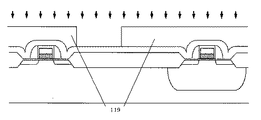
次に図5に示すように、フォトレジスト119をパターニングしN型不純物である砒素またはリンをイオン注入法により不純物濃度が1×10¹⁶〜1×10¹⁸atoms/cm3程度となるようにドーピングし、NMOSトランジスタのソースおよびドレインのN型低濃度不純物領域120を形成する。そしてフォトレジスト除去後、図6に示す様に、新たにフォトレジスト119をパターニングしP型不純物であるボロンないしBF2をイオン注入法により不純物濃度が1×1016〜1×1018atoms/cm3程度となるようにドーピングし、PMOSトランジスタのドレインのP型低濃度不純物領域121を形成する。
【0030】
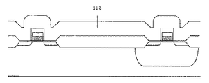
次に図7に示す様に、ゲート電極側壁にサイドスペーサーを形成するためCVD法(化学気相成長法)により絶縁膜122を被着する。このとき、ゲート電極のマスク材として絶縁膜に酸化膜を用いた場合はスペーサー材として窒化膜を、マスク材として窒化膜を用いた場合はスペーサー材として酸化膜を堆積する。これはスペーサーエッチの際、ゲートのマスク材とスペーサー材のエッチングの選択比をとるためである。その後RIE異方性ドライエッチングを行うことで図8のようにサイドスペーサー123を形成する。
【0031】
その後、図9に示すように、CVD法もしくはスパッタ法により例えば1000Åの膜厚の第2の多結晶シリコン118を堆積させる。そして低濃度のP型抵抗体を形成するために、第2の多結晶シリコン118全面にP型不純物であるBF2をドーズ量を例えば1×10¹⁴atoms/cm2でイオン注入する。尚、BF2の代わりにボロンを用いても構わない。その後図10に示すように低濃度のN型抵抗体領域をフォトレジスト119でパターニングし選択的にリンを、例えばドーズ量3×1014atoms/cm2イオン注入する。このときN型抵抗体を安定して形成するためにリンのドーズ量はBF2ドーズ量に対して2倍以上にする必要がある。尚、リンの代わりに砒素を用いても構わない。このように後にN型となる多結晶シリコン抵抗体領域に予めP型抵抗体のシート抵抗値を設定するボロンを導入し、後にN型不純物であるリンもしくは砒素でN型抵抗体領域を打ち返すことで、効率よくシート抵抗値を上げることが可能となる。尚、P型抵抗体領域およびN型抵抗体領域にフォトレジストなどのマスクをそれぞれ用いてイオン注入を打ち分ける方法をとっても構わない。
【0032】
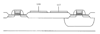
その後フォトレジスト119を除去後、フォトレジストでパターニングしRIE異方性ドライエッチングをすることで、図11のように第1導電型のN型多結晶シリコン抵抗体116と、第2導電型のP型多結晶シリコン抵抗体117を形成する。
【0033】
次に図12に示す様に、フォトレジスト119をパターニングしN型不純物である砒素をイオン注入法によりドーズ量5×10¹⁵atoms/cm2でドープすることで、第1導電型であるN型の第2多結晶シリコン抵抗体116にアルミニウム配線と十分なコンタクトをとるための高濃度不純物領域108と、NMOSトランジスタのソースおよびドレインとなるN型高濃度不純物領域103を同時に形成する。また図10における第2多結晶シリコン抵抗体のN型不純物導入を省略して、代わりに図12においてのN型高濃度不純物をN型抵抗体全域へドーピングし、比較的低抵抗のN型抵抗体を形成することも可能である。
【0034】
その後フォトレジスト除去した後、図13に示す様に、フォトレジスト119をパターニングしP型不純物であるBF2をイオン注入法によりドーズ量5×10¹⁵atoms/cm2でドープすることで、第2導電型であるP型の第2多結晶シリコン抵抗体117にアルミニウム配線と十分なコンタクトをとるための高濃度不純物領域109と、PMOSトランジスタのソースおよびドレインとなるP型高濃度不純物領域104を同時に形成する。また図13において、P型高濃度不純物をP型抵抗体全域へドーピングし、比較的低抵抗のP型抵抗体を形成することも可能である。
【0035】
その後は図示しないが従来の半導体プロセスと同様に、中間絶縁膜の形成、コンタクトホール形成、アルミニウム配線パターンの形成、保護膜の形成とそのパターニングを経て相補型MOS半導体装置が形成される。
【0036】
以上本発明の実施の形態をP型半導体基板を用いた実施例により説明してきたが、基板の極性を逆にしてN型の半導体基板を用いたN基板Pウェル型のP+単極ゲートCMOSによっても以上に説明してきた内容と原理に同じく低電圧動作、低消費電力、低コストである半導体装置の提供は可能である。
【0037】
【発明の効果】
上述したように、本発明はCMOSと抵抗体とを含むパワーマネージメント半導体装置やアナログ半導体装置において、CMOSのゲート電極の導電型をNMOS、PMOSともにP型多結晶シリコンと高融点金属シリサイドの積層構造であるP型ポリサイド構造の製造方法であり、さらに分圧回路やCR回路に用いられる抵抗体をゲート電極とは異なる別層の多結晶シリコンで形成することでより高精度の抵抗体を有することができる半導体装置の製造方法であるため、従来のN+多結晶シリコンゲート単極のCMOSやチャネルとゲート電極の極性が同じ同極ゲートCMOSに比べ、コスト、工期、素子の性能の面で有利であり、またより高機能、高精度なパワーマネージメント半導体装置やアナログ半導体装置の実現を可能とする。
【図面の簡単な説明】
【図1】本発明のCMOS半導体装置の一実施例を示す模式的断面図。
【図2】本発明のCMOS半導体装置の製造方法を示す工程順断面図。
【図3】本発明のCMOS半導体装置の製造方法を示す工程順断面図。
【図4】本発明のCMOS半導体装置の製造方法を示す工程順断面図。
【図5】本発明のCMOS半導体装置の製造方法を示す工程順断面図。
【図6】本発明のCMOS半導体装置の製造方法を示す工程順断面図。
【図7】本発明のCMOS半導体装置の製造方法を示す工程順断面図。
【図8】本発明のCMOS半導体装置の製造方法を示す工程順断面図。
【図9】本発明のCMOS半導体装置の製造方法を示す工程順断面図。
【図10】本発明のCMOS半導体装置の製造方法を示す工程順断面図。
【図11】本発明のCMOS半導体装置の製造方法を示す工程順断面図。
【図12】本発明のCMOS半導体装置の製造方法を示す工程順断面図。
【図13】本発明のCMOS半導体装置の製造方法を示す工程順断面図。
【図14】従来のCMOS半導体装置の一実施例を示す模式的断面図。
【図15】従来のCMOS半導体装置の一実施例を示す模式的断面図。
【図16】従来のCMOS半導体装置の一実施例を示す模式的断面図。
【符号の説明】
101、201 P型半導体基板
102、202 Nウェル
103、203 N+
104、204 P+
105、205 ゲート絶縁膜
106、206 フィールド絶縁膜
107、207 P+多結晶シリコン
108、208 N+多結晶シリコン
109 209 P+多結晶シリコン
110、210 N−多結晶シリコン
111、211 P−多結晶シリコン
112、212 高融点金属シリサイド
113 絶縁膜
114、214 NMOS
115、215 PMOS
116、216 N−抵抗体
117、217 P−抵抗体
118 多結晶シリコン
119 フォトレジスト
120 N−
121 P−
122 絶縁膜
123 サイドスペーサー
221 N+多結晶シリコン
222 P+多結晶シリコン[0001]
BACKGROUND OF THE INVENTION
The present invention relates to a complementary MOS semiconductor device having a resistance circuit, which requires low voltage operation, low power consumption and high driving capability, particularly a voltage detector (hereinafter referred to as VD) and a constant voltage regulator (Voltage). The present invention relates to a power management semiconductor device such as a regulator (hereinafter referred to as VR) and a switching regulator (hereinafter referred to as SWR) and an analog semiconductor device such as an operational amplifier and a comparator.
[0002]
[Prior art]
Conventionally, many complementary MOS semiconductor devices having a resistance circuit using a resistor such as polycrystalline silicon have been used. FIG. 14 shows an embodiment of a structure of a semiconductor device having a conventional resistance circuit. An N-channel MOS transistor (hereinafter referred to as NMOS) whose gate electrode formed on the P-type semiconductor substrate is made of N + type polycrystalline silicon, and a gate electrode formed in the N well region is also made of N + type polycrystalline silicon. Complementary MOS structure (Complementary MOS, hereinafter referred to as CMOS) composed of a P channel type MOS transistor (hereinafter referred to as PMOS), and a voltage dividing circuit or time constant for dividing the voltage formed on the field insulating film It is comprised from the resistor used for the CR circuit etc. which set up.
[0003]
[Problems to be solved by the invention]
In the complementary MOS (CMOS) semiconductor device having this resistance circuit, N + type polycrystalline silicon is often used as the polarity of the gate electrode because of its ease of manufacture and stability. In this case, the NMOS transistor is a surface channel type due to the relationship between the work function of the gate electrode and the semiconductor substrate (well), but in the case of the PMOS transistor, the threshold voltage is about −− due to the relationship between the work function of the gate electrode and the semiconductor substrate. 1V. For this reason, if impurity implantation is performed to lower the threshold voltage, a buried channel is formed which forms a channel inside the substrate slightly from the surface. The buried channel has an advantage that the mobility is large because carriers pass through the substrate, but if the threshold voltage is lowered, the subthreshold characteristic is extremely deteriorated and the leakage current is increased. Therefore, it is difficult to reduce the voltage and shorten the channel of the PMOS transistor as compared with the NMOS transistor.
[0004]
Further, as a structure capable of lowering the voltage of both the NMOS transistor and the PMOS transistor, there is a homopolar gate structure in which the polarity of the gate electrode is made equal to the polarity of the transistor. This structure N + -type polycrystalline silicon to a gate electrode of the NMOS transistor, becomes possible low voltage both reduces the leakage current becomes a surface channel-type for using the P + -type polycrystalline silicon PMOS transistor. However, the number of manufacturing steps increases due to the separate polarity of the gate electrode, resulting in an increase in manufacturing cost and manufacturing period, and in the inverter circuit, which is the most basic circuit element, usually for improving area efficiency. The gate electrode of the NMOS transistor and the PMOS transistor is a polycide structure consisting of a single layer of polycrystalline silicon or a stack of polycrystalline silicon and a refractory metal silicide, which is planarly continuous from the NMOS transistor to the PMOS transistor, avoiding connection through metal. However, when it is formed from a polycrystalline silicon single layer as shown in FIG. 4, the impedance of the PN junction in the polycrystalline silicon is high and not practical, and the polycide structure as shown in FIG. In some cases, N-type and P-type impurities are refractory gold during heat treatment in the process. There is a problem in terms of cost and characteristics, such as diffusion of metal silicide into the gate electrodes of opposite conductivity type at high speed, resulting in a change in work function and unstable threshold voltage.
[0005]
[Means for Solving the Problems]
In order to solve the above problems, the present invention uses the following means.
[0006]
(1) A step of forming an element isolation insulating film by thermal oxidation on a semiconductor substrate, a step of forming a gate insulating film by thermal oxidation, and depositing a first polycrystalline silicon film of 500 to 2500 mm on the gate insulating film And a step of doping the first polycrystalline silicon film with an impurity so that the impurity concentration is 1 × 10 18 atoms / cm 3 or more to make the conductivity type of the first polycrystalline silicon film P type, A step of depositing a refractory metal silicide having a thickness of 500 to 2500 on the first P-type polycrystalline silicon, a step of depositing an insulating film having a thickness of 500 to 3000 上 on the refractory metal silicide, and a first P-type polycrystal Etching the crystalline silicon, the refractory metal silicide and the insulating film to form a stacked polycide gate electrode; and forming a first conductive layer in the low-concentration diffusion region of the first conductivity type MOS transistor; Doping the impurity of the
[0007]
(2) The semiconductor device manufacturing method is characterized in that the impurity introduction method into the first polycrystalline silicon film is boron ion implantation.
[0008]
(3) The semiconductor device manufacturing method is characterized in that the impurity introduction method into the first polycrystalline silicon film is BF 2 ion implantation.
[0009]
(4) Manufacturing of a semiconductor device characterized in that the impurity introduction method to the first polycrystalline silicon film is a Doped-CVD method in which impurities are simultaneously mixed when the first polycrystalline silicon film is deposited. It was a method.
[0010]
(5) The semiconductor device manufacturing method is characterized in that the insulating film deposited on the refractory metal silicide is composed of an oxide film.
[0011]
(6) Manufacture of a semiconductor device characterized in that when the insulating film deposited on the refractory metal silicide is an oxide film, the insulating film serving as a material of the side spacer formed on the side wall of the polycide gate electrode is a nitride film. It was a method.
[0012]
(7) The semiconductor device manufacturing method is characterized in that the insulating film deposited on the refractory metal silicide is formed of a nitride film.
[0013]
(8) Manufacture of a semiconductor device characterized in that when the insulating film deposited on the refractory metal silicide is a nitride film, the insulating film serving as a material of the side spacer formed on the side wall of the polycide gate electrode is an oxide film. It was a method.
[0014]
(9) The semiconductor device manufacturing method is characterized in that the insulating film deposited on the refractory metal silicide has a laminated structure of an oxide film, a nitride film, and another oxide film.
[0015]
(10) When the insulating film deposited on the refractory metal silicide is a laminated structure and the uppermost layer is an oxide film, the insulating film serving as a material of the side spacer formed on the side wall of the polycide gate electrode is a nitride film. The method for manufacturing a semiconductor device is as follows.
[0016]
(11) Impurity doping of a first conductivity type of 1 × 10 19 atoms / cm 3 or more to a part and the whole of the first region of the second polycrystalline silicon film is the first conductivity type MOS transistor. Simultaneously with the diffusion region doping, impurity doping of the second conductivity type of 1 × 10 19 atoms / cm 3 or more to a part and the whole of the second region of the second polycrystalline silicon film is the second conductivity. The method of manufacturing a semiconductor device is characterized by being simultaneously with the diffusion region doping of the MOS transistor of the type.
[0017]
DETAILED DESCRIPTION OF THE INVENTION
Hereinafter, embodiments of the present invention will be described in detail with reference to the drawings.
FIG. 1 is a cross-sectional view showing an embodiment of a CMOS semiconductor device having a resistance circuit of the present invention.
[0018]
In this embodiment, an N-type well
[0019]
In this embodiment, the N-type second polycrystalline silicon resistor 116 of the first conductivity type and the P-type second
[0020]
The N-type polycrystalline silicon resistor 116 has a high-resistance region 110 and high-
[0021]
For example, the sheet resistance value is used in the range of several kΩ / □ to several tens of kΩ / □ in a normal voltage dividing circuit, although it depends on the use of the resistor. The impurity at this time is boron or BF 2 in the P-
[0022]
FIG. 1 shows both the N-resistor 116 and the P-
[0023]
By making the gate electrode P + type in this way, the PMOS transistor becomes a surface channel, and even when the threshold voltage is set low, it is possible to suppress the leakage current as compared with the buried channel. On the other hand, in the case of an NMOS transistor, when the gate electrode is made P + type, it becomes a buried channel, but arsenic having a diffusion coefficient smaller than that of boron is used for impurity implantation for lowering the threshold voltage. For this reason, it is closer to the surface channel than the PMOS transistor of the N + type gate electrode, and arsenic has the property of condensing near the interface between the silicon and the oxide film, and therefore closer to the surface channel. Therefore, the N-type MOS transistor can suppress the leakage current even when the threshold voltage is lowered, and can operate at a low voltage. In addition, by making the gates of both the N-type MOS transistor and the P-type MOS transistor P + type with respect to the homopolar gate structure, the manufacturing process can be simplified and the cost can be reduced.
[0024]
Further, in FIG. 1, low concentration impurity diffusion layers N-120 and P-121 are formed in the source and drain for the purpose of improving channel length modulation, suppressing reliability deterioration due to hot carriers, and improving drain breakdown voltage, which are important in analog circuits. And a MOS transistor structure having a so-called Lightly Doped Drain (LDD) structure having high-concentration impurity diffusion layers N + 103 and P + 104 provided at a distance of the
[0025]
In the LDD structure shown in FIG. 1, for example, a low-concentration impurity diffusion layer is formed by ion implantation and heat treatment, an insulating film is then deposited by CVD (chemical vapor deposition), and anisotropic dry etching is performed to form side spacers. And a high-concentration impurity diffusion layer is provided by ion implantation in a self-aligning manner. In the case of N-120 of NMOS 114, the low concentration impurity diffusion layer uses phosphorus or arsenic as an impurity and has a concentration of about 1 × 10 16 to 1 × 10 18 atoms / cm 3 , and in the case of P-121 of
[0026]
As described above, the CMOS using the P + polycrystalline silicon single electrode as the gate electrode according to the present invention is more effective for low voltage operation and low power consumption than the conventional CMOS using the N + polycrystalline silicon single electrode as the gate electrode. Furthermore, by using a semiconductor device having a polycrystalline silicon resistor different from the gate electrode and an LDD structure transistor, high functions and high precision required for an analog circuit can be achieved.
[0027]
Next, an example of the manufacturing process of the semiconductor device shown in FIG. 1 will be described with reference to FIG.
[0028]
For example, phosphorus is ion-implanted into the P-type
[0029]
Next, as shown in FIG. 5, the
[0030]
Next, as shown in FIG. 7, an insulating film 122 is deposited by CVD (chemical vapor deposition) to form side spacers on the side walls of the gate electrode. At this time, a nitride film is deposited as a spacer material when an oxide film is used as an insulating film as a mask material for the gate electrode, and an oxide film is deposited as a spacer material when a nitride film is used as a mask material. This is because the etching ratio of the gate mask material and the spacer material is taken during the spacer etching. Thereafter, RIE anisotropic dry etching is performed to form
[0031]
Thereafter, as shown in FIG. 9, a second polycrystalline silicon 118 having a thickness of, eg, 1000 mm is deposited by CVD or sputtering. In order to form a low-concentration P-type resistor, BF 2 , which is a P-type impurity, is ion-implanted into the entire surface of the second polycrystalline silicon 118 at a dose of, for example, 1 × 10 14 atoms / cm 2 . Note that boron may be used instead of BF 2 . Thereafter, as shown in FIG. 10, the low-concentration N-type resistor region is patterned with a
[0032]
Then, after removing the
[0033]
Next, as shown in FIG. 12, the
[0034]
Thereafter, after removing the photoresist, as shown in FIG. 13, the
[0035]
Thereafter, although not shown, a complementary MOS semiconductor device is formed through the formation of an intermediate insulating film, the formation of contact holes, the formation of an aluminum wiring pattern, the formation of a protective film, and the patterning as in the conventional semiconductor process.
[0036]
Although the embodiment of the present invention has been described with the example using the P-type semiconductor substrate, the N-substrate P-well type P + single-pole gate CMOS using the N-type semiconductor substrate with the substrate polarity reversed is used. However, it is possible to provide a semiconductor device that has low voltage operation, low power consumption, and low cost in the same manner as described above.
[0037]
【Effect of the invention】
As described above, the present invention is a power management semiconductor device or analog semiconductor device including a CMOS and a resistor. In the CMOS, the gate electrode conductivity type is a stacked structure of P-type polycrystalline silicon and refractory metal silicide for both NMOS and PMOS. The P-type polycide structure is a manufacturing method of the P-type polycide structure, and the resistor used for the voltage dividing circuit and the CR circuit is formed of a different layer of polycrystalline silicon different from the gate electrode to have a more accurate resistor. This method is advantageous in terms of cost, construction period, and device performance compared to conventional N + polycrystalline silicon gate single-polar CMOS and homopolar gate CMOS having the same channel and gate electrode polarity. In addition, it enables the realization of power management semiconductor devices and analog semiconductor devices with higher functionality and higher accuracy.
[Brief description of the drawings]
FIG. 1 is a schematic cross-sectional view showing an embodiment of a CMOS semiconductor device of the present invention.
FIG. 2 is a cross-sectional view in order of steps showing a method for manufacturing a CMOS semiconductor device of the present invention.
3 is a cross-sectional view in order of the steps showing the method of manufacturing a CMOS semiconductor device according to the present invention; FIG.
FIG. 4 is a cross-sectional view in order of steps showing a method for manufacturing a CMOS semiconductor device of the present invention.
FIG. 5 is a cross-sectional view in order of steps showing the method for manufacturing a CMOS semiconductor device of the present invention.
6 is a cross-sectional view in order of the steps showing the method of manufacturing a CMOS semiconductor device according to the present invention; FIG.
7 is a cross-sectional view in order of the steps showing the method of manufacturing a CMOS semiconductor device of the present invention; FIG.
8 is a cross-sectional view in order of the steps showing the method of manufacturing a CMOS semiconductor device of the present invention; FIG.
9 is a cross-sectional view in order of the steps showing the method of manufacturing a CMOS semiconductor device of the present invention; FIG.
10 is a cross-sectional view in order of the steps showing the method of manufacturing a CMOS semiconductor device of the present invention; FIG.
11 is a cross-sectional view in order of the steps showing the method of manufacturing a CMOS semiconductor device of the present invention; FIG.
12 is a cross-sectional view in order of the steps showing the method of manufacturing a CMOS semiconductor device of the present invention; FIG.
13 is a cross-sectional view in order of the steps showing the method for manufacturing a CMOS semiconductor device of the present invention; FIG.
FIG. 14 is a schematic cross-sectional view showing an example of a conventional CMOS semiconductor device.
FIG. 15 is a schematic cross-sectional view showing an example of a conventional CMOS semiconductor device.
FIG. 16 is a schematic cross-sectional view showing an example of a conventional CMOS semiconductor device.
[Explanation of symbols]
101, 201 P-
104, 204 P +
105, 205
115, 215 PMOS
116, 216 N-
121 P-
122
Claims (11)
熱酸化によるゲート絶縁膜を形成する工程と、
前記ゲート絶縁膜上に500Å〜2500Åの第1の多結晶シリコン膜を堆積する工程と、
前記第1の多結晶シリコン膜に不純物濃度が1×10¹⁸atoms/cm3以上となるように不純物のドーピングを行い前記第1の多結晶シリコン膜の導電型をP型にする工程と、
前記第1のP型多結晶シリコン上に500Å〜2500Åからなる高融点金属シリサイドを堆積する工程と、
前記高融点金属シリサイド上に500Å〜3000Åからなる絶縁膜を堆積する工程と、
前記第1のP型多結晶シリコンと前記高融点金属シリサイドと前記絶縁膜をエッチングし積層構造を有するポリサイドゲート電極を形成する工程と、
第1の導電型のMOSトランジスタの低濃度拡散領域に第1の導電型の不純物を1×10¹⁶〜1×10¹⁸atoms/cm3ドーピングする工程と、
第2の導電型のMOSトランジスタの低濃度拡散領域に第2の導電型の不純物を1×10¹⁶〜1×10¹⁸atoms/cm3ドーピングする工程と、
前記ポリサイドゲート電極上にサイドスペーサー形成用の絶縁膜を堆積する工程と、
異方性ドライエッチで前記サイドスペーサー形成用の絶縁膜をエッチングし前記ポリサイドゲート電極側壁にサイドスペーサーを形成する工程と、
前記ポリサイドゲート電極の形成後に、前記素子分離絶縁膜上に500Å〜2500Åからなる第2の多結晶シリコン膜を堆積する工程と、
前記第2の多結晶シリコン膜の全域ないしは前記第2の多結晶シリコン膜の第1の領域に第2の導電型の不純物を1×10¹⁴〜9×10¹⁸atoms/cm3ドーピングする工程と、
前記第2の多結晶シリコン膜の第2の領域に第1の導電型の不純物を1×10¹⁴〜9×10¹⁸atoms/cm3ドーピングする工程と、
前記第2の多結晶シリコン膜をエッチングし第2の多結晶シリコン膜からなる第1導電型の抵抗体および第2導電型の抵抗体を形成する工程と、
前記第1導電型の抵抗体の一部ないし全域に1×10¹⁹atoms/cm3以上の第1の導電型の不純物をドーピングする工程と、
前記第2導電型の抵抗体の一部ないし全域に1×10¹⁹atoms/cm3以上の第2の導電型の不純物をドーピングする工程と、
前記半導体基板上に中間絶縁膜を形成する工程と、
前記半導体基板上の前記中間絶縁膜にコンタクト孔を形成する工程と、
前記コンタクト孔に金属配線を設ける工程と、からなる半導体装置の製造方法。Forming an element isolation insulating film by thermal oxidation on a semiconductor substrate;
Forming a gate insulating film by thermal oxidation;
Depositing a first polycrystalline silicon film having a thickness of 500 to 2500 on the gate insulating film;
A step of the conductivity type of said first polycrystalline silicon film subjected to doping impurity so that the impurity concentration in the first polycrystalline silicon film is 1 × 10 18 atoms / cm 3 or more P-type,
Depositing a refractory metal silicide of 500 to 2500 on the first P-type polycrystalline silicon;
Depositing an insulating film of 500 to 3000 mm on the refractory metal silicide;
Etching the first P-type polycrystalline silicon, the refractory metal silicide, and the insulating film to form a polycide gate electrode having a laminated structure ;
Doping the impurity of the first conductivity type to 1 × 10 16 to 1 × 10 18 atoms / cm 3 in the low concentration diffusion region of the MOS transistor of the first conductivity type;
Doping a second conductivity type impurity into the low-concentration diffusion region of the second conductivity type MOS transistor by 1 × 10 16 to 1 × 10 18 atoms / cm 3 ;
Depositing an insulating film for forming a side spacer on the polycide gate electrode;
Etching the insulating film for forming the side spacer by anisotropic dry etching to form a side spacer on the side wall of the polycide gate electrode; and
Depositing a second polycrystalline silicon film of 500 to 2500 on the element isolation insulating film after forming the polycide gate electrode ;
Doping the second conductive type impurity with 1 × 10 14 to 9 × 10 18 atoms / cm 3 in the entire region of the second polycrystalline silicon film or in the first region of the second polycrystalline silicon film; ,
Doping the second region of the second polycrystalline silicon film with a first conductivity type impurity of 1 × 10 14 to 9 × 10 18 atoms / cm 3 ;
Etching the second polycrystalline silicon film to form a first conductive type resistor and a second conductive type resistor made of the second polycrystalline silicon film;
Doping a first conductive type impurity of 1 × 10 19 atoms / cm 3 or more to a part or all of the first conductive type resistor;
Doping a second conductive type impurity of 1 × 10 19 atoms / cm 3 or more to a part or all of the second conductive type resistor;
Forming an intermediate insulating film on the semiconductor substrate;
Forming a contact hole in the intermediate insulating film on the semiconductor substrate;
Method of manufacturing a step of providing a metal wiring on the contact hole, a semiconductor device comprising a.
Priority Applications (4)
| Application Number | Priority Date | Filing Date | Title |
|---|---|---|---|
| JP2001188050A JP4898024B2 (en) | 2001-06-21 | 2001-06-21 | Manufacturing method of semiconductor device |
| PCT/JP2002/006072 WO2003001592A1 (en) | 2001-06-21 | 2002-06-18 | Method for manufacturing semiconductor device |
| US10/398,035 US7528032B2 (en) | 2001-06-21 | 2002-06-18 | Method for manufacturing semiconductor device |
| CNB028027035A CN1246896C (en) | 2001-06-21 | 2002-06-18 | Method for manufacturing semiconductor device |
Applications Claiming Priority (1)
| Application Number | Priority Date | Filing Date | Title |
|---|---|---|---|
| JP2001188050A JP4898024B2 (en) | 2001-06-21 | 2001-06-21 | Manufacturing method of semiconductor device |
Publications (2)
| Publication Number | Publication Date |
|---|---|
| JP2003007847A JP2003007847A (en) | 2003-01-10 |
| JP4898024B2 true JP4898024B2 (en) | 2012-03-14 |
Family
ID=19027237
Family Applications (1)
| Application Number | Title | Priority Date | Filing Date |
|---|---|---|---|
| JP2001188050A Expired - Fee Related JP4898024B2 (en) | 2001-06-21 | 2001-06-21 | Manufacturing method of semiconductor device |
Country Status (4)
| Country | Link |
|---|---|
| US (1) | US7528032B2 (en) |
| JP (1) | JP4898024B2 (en) |
| CN (1) | CN1246896C (en) |
| WO (1) | WO2003001592A1 (en) |
Families Citing this family (12)
| Publication number | Priority date | Publication date | Assignee | Title |
|---|---|---|---|---|
| US7105912B2 (en) * | 2004-09-15 | 2006-09-12 | United Microelectronics Corp. | Resistor structure and method for manufacturing the same |
| US20060057813A1 (en) * | 2004-09-15 | 2006-03-16 | Cheng-Hsiung Chen | Method of forming a polysilicon resistor |
| GB2439357C (en) * | 2006-02-23 | 2008-08-13 | Innos Ltd | Integrated circuit manufacturing |
| JP2008205053A (en) * | 2007-02-17 | 2008-09-04 | Seiko Instruments Inc | Semiconductor device |
| US20100052072A1 (en) * | 2008-08-28 | 2010-03-04 | Taiwan Semiconductor Manufacturing Company, Ltd. | Dual gate structure on a same chip for high-k metal gate technology |
| KR20100076256A (en) * | 2008-12-26 | 2010-07-06 | 주식회사 동부하이텍 | Method of manufacturing a polysilicon-insulator-polysilicon |
| US9184097B2 (en) * | 2009-03-12 | 2015-11-10 | System General Corporation | Semiconductor devices and formation methods thereof |
| JP5546298B2 (en) * | 2010-03-15 | 2014-07-09 | セイコーインスツル株式会社 | Manufacturing method of semiconductor circuit device |
| CN102110593B (en) * | 2010-12-15 | 2012-05-09 | 无锡中微晶园电子有限公司 | Method for improving stability of polysilicon thin-film resistor |
| GB2610886B (en) * | 2019-08-21 | 2023-09-13 | Pragmatic Printing Ltd | Resistor geometry |
| GB2587793B (en) | 2019-08-21 | 2023-03-22 | Pragmatic Printing Ltd | Electronic circuit comprising transistor and resistor |
| CN114373716B (en) * | 2022-03-22 | 2022-06-17 | 晶芯成(北京)科技有限公司 | Integrated device and method of making the same |
Family Cites Families (28)
| Publication number | Priority date | Publication date | Assignee | Title |
|---|---|---|---|---|
| US530502A (en) * | 1894-12-11 | Strawboard-lining machine | ||
| JPS48102579A (en) * | 1972-04-05 | 1973-12-22 | ||
| US5610089A (en) * | 1983-12-26 | 1997-03-11 | Hitachi, Ltd. | Method of fabrication of semiconductor integrated circuit device |
| JPS6473676A (en) * | 1987-09-16 | 1989-03-17 | Hitachi Ltd | Semiconductor integrated circuit device |
| JPH0342869A (en) * | 1989-07-10 | 1991-02-25 | Seiko Instr Inc | Manufacture of semiconductor device |
| JPH03114267A (en) * | 1989-09-28 | 1991-05-15 | Hitachi Ltd | Semiconductor device and manufacture thereof |
| JPH0465160A (en) * | 1990-07-05 | 1992-03-02 | Oki Electric Ind Co Ltd | Semiconductor device |
| JPH0484428A (en) * | 1990-07-27 | 1992-03-17 | Nec Corp | Manufacture of semiconductor device |
| JPH05267604A (en) * | 1991-05-08 | 1993-10-15 | Seiko Instr Inc | Manufacture of semiconductor device |
| US5489547A (en) * | 1994-05-23 | 1996-02-06 | Texas Instruments Incorporated | Method of fabricating semiconductor device having polysilicon resistor with low temperature coefficient |
| JP3297784B2 (en) * | 1994-09-29 | 2002-07-02 | ソニー株式会社 | Method of forming diffusion layer resistance |
| JPH08186179A (en) * | 1994-12-28 | 1996-07-16 | Sony Corp | Complementary semiconductor device |
| US5618749A (en) * | 1995-03-31 | 1997-04-08 | Yamaha Corporation | Method of forming a semiconductor device having a capacitor and a resistor |
| JP3719618B2 (en) * | 1996-06-17 | 2005-11-24 | 松下電器産業株式会社 | Semiconductor device and manufacturing method thereof |
| KR100200488B1 (en) * | 1996-10-14 | 1999-06-15 | 윤종용 | Method for manufacturing semiconductor device having thin film resistance |
| JPH10303372A (en) * | 1997-01-31 | 1998-11-13 | Sanyo Electric Co Ltd | Semiconductor integrated circuit and method of manufacturing the same |
| KR100215845B1 (en) * | 1997-03-17 | 1999-08-16 | 구본준 | Semiconductor device manufacturing method |
| US5959343A (en) * | 1997-04-21 | 1999-09-28 | Seiko Instruments R&D Center Inc. | Semiconductor device |
| US5953599A (en) * | 1997-06-12 | 1999-09-14 | National Semiconductor Corporation | Method for forming low-voltage CMOS transistors with a thin layer of gate oxide and high-voltage CMOS transistors with a thick layer of gate oxide |
| JPH11111978A (en) * | 1997-09-30 | 1999-04-23 | Toshiba Corp | Semiconductor device |
| KR100272176B1 (en) * | 1998-09-30 | 2000-12-01 | 김덕중 | Method fabricating bicdmos device |
| JP2000114395A (en) * | 1998-10-09 | 2000-04-21 | Sony Corp | Semiconductor device and method of manufacturing the same |
| JP2000183175A (en) * | 1998-12-10 | 2000-06-30 | Sanyo Electric Co Ltd | Manufacture of semiconductor device |
| JP2000243860A (en) * | 1999-02-23 | 2000-09-08 | Hitachi Ltd | Semiconductor device and manufacturing method thereof |
| JP2002237524A (en) * | 2001-02-09 | 2002-08-23 | Seiko Instruments Inc | Complementary MOS semiconductor device |
| JP2002280459A (en) * | 2001-03-21 | 2002-09-27 | Kawasaki Microelectronics Kk | Manufacturing method of integrated circuit |
| JP2003158198A (en) * | 2001-09-07 | 2003-05-30 | Seiko Instruments Inc | Complementary MOS semiconductor device |
| JP2003273233A (en) * | 2002-01-10 | 2003-09-26 | Seiko Instruments Inc | Semiconductor device and method of manufacturing the same |
-
2001
- 2001-06-21 JP JP2001188050A patent/JP4898024B2/en not_active Expired - Fee Related
-
2002
- 2002-06-18 WO PCT/JP2002/006072 patent/WO2003001592A1/en not_active Ceased
- 2002-06-18 US US10/398,035 patent/US7528032B2/en not_active Expired - Fee Related
- 2002-06-18 CN CNB028027035A patent/CN1246896C/en not_active Expired - Fee Related
Also Published As
| Publication number | Publication date |
|---|---|
| CN1466776A (en) | 2004-01-07 |
| CN1246896C (en) | 2006-03-22 |
| US20050074929A1 (en) | 2005-04-07 |
| US7528032B2 (en) | 2009-05-05 |
| WO2003001592A1 (en) | 2003-01-03 |
| JP2003007847A (en) | 2003-01-10 |
Similar Documents
| Publication | Publication Date | Title |
|---|---|---|
| KR100883701B1 (en) | Complementary Metal Oxide Semiconductor Device | |
| CN100487911C (en) | Bimetallic grid transistor for CMOS process and manufacturing method thereof | |
| JP4976624B2 (en) | Complementary MOS semiconductor device and manufacturing method thereof | |
| US5436482A (en) | MOSFET with assymetric lightly doped source-drain regions | |
| JP2707977B2 (en) | MOS type semiconductor device and method of manufacturing the same | |
| JP2002170886A (en) | Semiconductor device for reference voltage and method of manufacturing the same | |
| JP4898024B2 (en) | Manufacturing method of semiconductor device | |
| CN100543999C (en) | CMOS semiconductor device and manufacturing method thereof | |
| JP2004088064A (en) | Semiconductor device and method of manufacturing the same | |
| JP4865152B2 (en) | Manufacturing method of semiconductor device | |
| US20080093666A1 (en) | Semiconductor Device and Manufacturing Method Thereof | |
| CN116487381A (en) | Medium and high voltage MOS device, layout structure and manufacturing method thereof | |
| US6078079A (en) | Semiconductor device and method of manufacturing the same | |
| CN100521154C (en) | Dual gate CMOS fabrication | |
| JPH04218925A (en) | Semiconductor device and manufacture thereof | |
| US20060134874A1 (en) | Manufacture method of MOS semiconductor device having extension and pocket | |
| US6613625B1 (en) | Method of manufacturing a semiconductor device | |
| KR20040066024A (en) | Semiconductor device and manufacturing method therefor | |
| CN1327511C (en) | Method for fg. seiconductor device | |
| JP4146121B2 (en) | Manufacturing method of semiconductor device | |
| GB2331845A (en) | Bicmos device | |
| JP2004063918A (en) | Lateral mos transistor | |
| JP4615682B2 (en) | Manufacturing method of MOS transistor | |
| US7700468B2 (en) | Semiconductor device and method of fabricating the same | |
| KR100260484B1 (en) | Thi film transistor and making method thereof |
Legal Events
| Date | Code | Title | Description |
|---|---|---|---|
| RD01 | Notification of change of attorney |
Free format text: JAPANESE INTERMEDIATE CODE: A7421 Effective date: 20040303 |
|
| A621 | Written request for application examination |
Free format text: JAPANESE INTERMEDIATE CODE: A621 Effective date: 20080319 |
|
| RD01 | Notification of change of attorney |
Free format text: JAPANESE INTERMEDIATE CODE: A7421 Effective date: 20091113 |
|
| A131 | Notification of reasons for refusal |
Free format text: JAPANESE INTERMEDIATE CODE: A131 Effective date: 20110802 |
|
| A521 | Request for written amendment filed |
Free format text: JAPANESE INTERMEDIATE CODE: A523 Effective date: 20110928 |
|
| TRDD | Decision of grant or rejection written | ||
| A01 | Written decision to grant a patent or to grant a registration (utility model) |
Free format text: JAPANESE INTERMEDIATE CODE: A01 Effective date: 20111220 |
|
| A01 | Written decision to grant a patent or to grant a registration (utility model) |
Free format text: JAPANESE INTERMEDIATE CODE: A01 |
|
| A61 | First payment of annual fees (during grant procedure) |
Free format text: JAPANESE INTERMEDIATE CODE: A61 Effective date: 20111226 |
|
| R150 | Certificate of patent or registration of utility model |
Free format text: JAPANESE INTERMEDIATE CODE: R150 Ref document number: 4898024 Country of ref document: JP Free format text: JAPANESE INTERMEDIATE CODE: R150 |
|
| FPAY | Renewal fee payment (event date is renewal date of database) |
Free format text: PAYMENT UNTIL: 20150106 Year of fee payment: 3 |
|
| S111 | Request for change of ownership or part of ownership |
Free format text: JAPANESE INTERMEDIATE CODE: R313113 |
|
| R350 | Written notification of registration of transfer |
Free format text: JAPANESE INTERMEDIATE CODE: R350 |
|
| R250 | Receipt of annual fees |
Free format text: JAPANESE INTERMEDIATE CODE: R250 |
|
| R250 | Receipt of annual fees |
Free format text: JAPANESE INTERMEDIATE CODE: R250 |
|
| S533 | Written request for registration of change of name |
Free format text: JAPANESE INTERMEDIATE CODE: R313533 |
|
| R350 | Written notification of registration of transfer |
Free format text: JAPANESE INTERMEDIATE CODE: R350 |
|
| R250 | Receipt of annual fees |
Free format text: JAPANESE INTERMEDIATE CODE: R250 |
|
| LAPS | Cancellation because of no payment of annual fees |