JP4878632B2 - Optical film thickness meter and thin film forming apparatus equipped with optical film thickness meter - Google Patents
Optical film thickness meter and thin film forming apparatus equipped with optical film thickness meter Download PDFInfo
- Publication number
- JP4878632B2 JP4878632B2 JP2009158798A JP2009158798A JP4878632B2 JP 4878632 B2 JP4878632 B2 JP 4878632B2 JP 2009158798 A JP2009158798 A JP 2009158798A JP 2009158798 A JP2009158798 A JP 2009158798A JP 4878632 B2 JP4878632 B2 JP 4878632B2
- Authority
- JP
- Japan
- Prior art keywords
- light
- film thickness
- optical film
- actual substrate
- substrate
- Prior art date
- Legal status (The legal status is an assumption and is not a legal conclusion. Google has not performed a legal analysis and makes no representation as to the accuracy of the status listed.)
- Active
Links
- 239000012788 optical film Substances 0.000 title claims description 83
- 239000010409 thin film Substances 0.000 title claims description 56
- 239000000758 substrate Substances 0.000 claims description 230
- 238000005259 measurement Methods 0.000 claims description 143
- 239000010408 film Substances 0.000 claims description 57
- 230000003287 optical effect Effects 0.000 claims description 48
- 238000007740 vapor deposition Methods 0.000 claims description 19
- 238000004544 sputter deposition Methods 0.000 claims description 18
- 239000000463 material Substances 0.000 claims description 15
- 238000012937 correction Methods 0.000 claims description 12
- 238000001704 evaporation Methods 0.000 claims description 5
- 238000000151 deposition Methods 0.000 claims description 3
- 230000008021 deposition Effects 0.000 claims description 3
- 230000005540 biological transmission Effects 0.000 description 31
- 239000013307 optical fiber Substances 0.000 description 28
- 230000008859 change Effects 0.000 description 25
- 238000002834 transmittance Methods 0.000 description 18
- 238000004364 calculation method Methods 0.000 description 12
- 230000015572 biosynthetic process Effects 0.000 description 11
- 229910004298 SiO 2 Inorganic materials 0.000 description 10
- 239000011521 glass Substances 0.000 description 9
- 238000000034 method Methods 0.000 description 8
- GUCVJGMIXFAOAE-UHFFFAOYSA-N niobium atom Chemical group [Nb] GUCVJGMIXFAOAE-UHFFFAOYSA-N 0.000 description 5
- 239000002356 single layer Substances 0.000 description 5
- 239000007789 gas Substances 0.000 description 4
- 239000004417 polycarbonate Substances 0.000 description 4
- -1 polyethylene terephthalate Polymers 0.000 description 4
- 230000002265 prevention Effects 0.000 description 4
- 230000008569 process Effects 0.000 description 4
- VYPSYNLAJGMNEJ-UHFFFAOYSA-N Silicium dioxide Chemical compound O=[Si]=O VYPSYNLAJGMNEJ-UHFFFAOYSA-N 0.000 description 3
- 230000004075 alteration Effects 0.000 description 3
- 238000001755 magnetron sputter deposition Methods 0.000 description 3
- 239000010955 niobium Substances 0.000 description 3
- 229910052758 niobium Inorganic materials 0.000 description 3
- 239000002245 particle Substances 0.000 description 3
- 229910001220 stainless steel Inorganic materials 0.000 description 3
- 239000010935 stainless steel Substances 0.000 description 3
- XKRFYHLGVUSROY-UHFFFAOYSA-N Argon Chemical compound [Ar] XKRFYHLGVUSROY-UHFFFAOYSA-N 0.000 description 2
- 230000008901 benefit Effects 0.000 description 2
- 230000007423 decrease Effects 0.000 description 2
- 238000001514 detection method Methods 0.000 description 2
- 238000010586 diagram Methods 0.000 description 2
- 230000000694 effects Effects 0.000 description 2
- 238000011065 in-situ storage Methods 0.000 description 2
- 238000000691 measurement method Methods 0.000 description 2
- 230000002093 peripheral effect Effects 0.000 description 2
- 230000035699 permeability Effects 0.000 description 2
- 239000000088 plastic resin Substances 0.000 description 2
- 229920001707 polybutylene terephthalate Polymers 0.000 description 2
- 239000005020 polyethylene terephthalate Substances 0.000 description 2
- 229920000139 polyethylene terephthalate Polymers 0.000 description 2
- 239000002994 raw material Substances 0.000 description 2
- 230000003595 spectral effect Effects 0.000 description 2
- 230000006641 stabilisation Effects 0.000 description 2
- 238000011105 stabilization Methods 0.000 description 2
- 229920000049 Carbon (fiber) Polymers 0.000 description 1
- 239000004677 Nylon Substances 0.000 description 1
- 239000004698 Polyethylene Substances 0.000 description 1
- 239000004743 Polypropylene Substances 0.000 description 1
- 239000004793 Polystyrene Substances 0.000 description 1
- NIXOWILDQLNWCW-UHFFFAOYSA-N acrylic acid group Chemical group C(C=C)(=O)O NIXOWILDQLNWCW-UHFFFAOYSA-N 0.000 description 1
- XECAHXYUAAWDEL-UHFFFAOYSA-N acrylonitrile butadiene styrene Chemical compound C=CC=C.C=CC#N.C=CC1=CC=CC=C1 XECAHXYUAAWDEL-UHFFFAOYSA-N 0.000 description 1
- 229920000122 acrylonitrile butadiene styrene Polymers 0.000 description 1
- 239000004676 acrylonitrile butadiene styrene Substances 0.000 description 1
- 238000004458 analytical method Methods 0.000 description 1
- 229910052786 argon Inorganic materials 0.000 description 1
- 239000005388 borosilicate glass Substances 0.000 description 1
- 239000004917 carbon fiber Substances 0.000 description 1
- 238000009826 distribution Methods 0.000 description 1
- 238000010894 electron beam technology Methods 0.000 description 1
- 230000008020 evaporation Effects 0.000 description 1
- 239000000835 fiber Substances 0.000 description 1
- 239000003365 glass fiber Substances 0.000 description 1
- 238000010438 heat treatment Methods 0.000 description 1
- 239000011261 inert gas Substances 0.000 description 1
- 150000002500 ions Chemical class 0.000 description 1
- 239000010410 layer Substances 0.000 description 1
- 238000004519 manufacturing process Methods 0.000 description 1
- 239000000203 mixture Substances 0.000 description 1
- 238000012986 modification Methods 0.000 description 1
- 230000004048 modification Effects 0.000 description 1
- 238000012544 monitoring process Methods 0.000 description 1
- 229920001778 nylon Polymers 0.000 description 1
- 238000005375 photometry Methods 0.000 description 1
- 238000009832 plasma treatment Methods 0.000 description 1
- 229920000515 polycarbonate Polymers 0.000 description 1
- 229920000573 polyethylene Polymers 0.000 description 1
- 229920001155 polypropylene Polymers 0.000 description 1
- 229920002223 polystyrene Polymers 0.000 description 1
- 238000012805 post-processing Methods 0.000 description 1
- 238000001028 reflection method Methods 0.000 description 1
- 238000002310 reflectometry Methods 0.000 description 1
- 239000011347 resin Substances 0.000 description 1
- 229920005989 resin Polymers 0.000 description 1
- 230000004043 responsiveness Effects 0.000 description 1
- 235000012239 silicon dioxide Nutrition 0.000 description 1
- 239000000377 silicon dioxide Substances 0.000 description 1
- 238000004088 simulation Methods 0.000 description 1
- 239000005361 soda-lime glass Substances 0.000 description 1
- 239000000126 substance Substances 0.000 description 1
Images


Classifications
-
- G—PHYSICS
- G01—MEASURING; TESTING
- G01B—MEASURING LENGTH, THICKNESS OR SIMILAR LINEAR DIMENSIONS; MEASURING ANGLES; MEASURING AREAS; MEASURING IRREGULARITIES OF SURFACES OR CONTOURS
- G01B11/00—Measuring arrangements characterised by the use of optical techniques
- G01B11/02—Measuring arrangements characterised by the use of optical techniques for measuring length, width or thickness
- G01B11/06—Measuring arrangements characterised by the use of optical techniques for measuring length, width or thickness for measuring thickness ; e.g. of sheet material
-
- C—CHEMISTRY; METALLURGY
- C23—COATING METALLIC MATERIAL; COATING MATERIAL WITH METALLIC MATERIAL; CHEMICAL SURFACE TREATMENT; DIFFUSION TREATMENT OF METALLIC MATERIAL; COATING BY VACUUM EVAPORATION, BY SPUTTERING, BY ION IMPLANTATION OR BY CHEMICAL VAPOUR DEPOSITION, IN GENERAL; INHIBITING CORROSION OF METALLIC MATERIAL OR INCRUSTATION IN GENERAL
- C23C—COATING METALLIC MATERIAL; COATING MATERIAL WITH METALLIC MATERIAL; SURFACE TREATMENT OF METALLIC MATERIAL BY DIFFUSION INTO THE SURFACE, BY CHEMICAL CONVERSION OR SUBSTITUTION; COATING BY VACUUM EVAPORATION, BY SPUTTERING, BY ION IMPLANTATION OR BY CHEMICAL VAPOUR DEPOSITION, IN GENERAL
- C23C14/00—Coating by vacuum evaporation, by sputtering or by ion implantation of the coating forming material
- C23C14/22—Coating by vacuum evaporation, by sputtering or by ion implantation of the coating forming material characterised by the process of coating
- C23C14/34—Sputtering
-
- C—CHEMISTRY; METALLURGY
- C23—COATING METALLIC MATERIAL; COATING MATERIAL WITH METALLIC MATERIAL; CHEMICAL SURFACE TREATMENT; DIFFUSION TREATMENT OF METALLIC MATERIAL; COATING BY VACUUM EVAPORATION, BY SPUTTERING, BY ION IMPLANTATION OR BY CHEMICAL VAPOUR DEPOSITION, IN GENERAL; INHIBITING CORROSION OF METALLIC MATERIAL OR INCRUSTATION IN GENERAL
- C23C—COATING METALLIC MATERIAL; COATING MATERIAL WITH METALLIC MATERIAL; SURFACE TREATMENT OF METALLIC MATERIAL BY DIFFUSION INTO THE SURFACE, BY CHEMICAL CONVERSION OR SUBSTITUTION; COATING BY VACUUM EVAPORATION, BY SPUTTERING, BY ION IMPLANTATION OR BY CHEMICAL VAPOUR DEPOSITION, IN GENERAL
- C23C14/00—Coating by vacuum evaporation, by sputtering or by ion implantation of the coating forming material
- C23C14/22—Coating by vacuum evaporation, by sputtering or by ion implantation of the coating forming material characterised by the process of coating
- C23C14/54—Controlling or regulating the coating process
- C23C14/542—Controlling the film thickness or evaporation rate
- C23C14/545—Controlling the film thickness or evaporation rate using measurement on deposited material
- C23C14/547—Controlling the film thickness or evaporation rate using measurement on deposited material using optical methods
-
- G—PHYSICS
- G01—MEASURING; TESTING
- G01B—MEASURING LENGTH, THICKNESS OR SIMILAR LINEAR DIMENSIONS; MEASURING ANGLES; MEASURING AREAS; MEASURING IRREGULARITIES OF SURFACES OR CONTOURS
- G01B11/00—Measuring arrangements characterised by the use of optical techniques
- G01B11/02—Measuring arrangements characterised by the use of optical techniques for measuring length, width or thickness
- G01B11/06—Measuring arrangements characterised by the use of optical techniques for measuring length, width or thickness for measuring thickness ; e.g. of sheet material
- G01B11/0616—Measuring arrangements characterised by the use of optical techniques for measuring length, width or thickness for measuring thickness ; e.g. of sheet material of coating
- G01B11/0625—Measuring arrangements characterised by the use of optical techniques for measuring length, width or thickness for measuring thickness ; e.g. of sheet material of coating with measurement of absorption or reflection
Description
本発明は光学式膜厚計及び光学式膜厚計を備えた薄膜形成装置に係り、特に、高精度な膜厚測定が可能な光学式膜厚計及び光学式膜厚計を備えた薄膜形成装置に関する。 The present invention relates to an optical film thickness meter and a thin film forming apparatus including an optical film thickness meter, and in particular, an optical film thickness meter capable of measuring a film thickness with high accuracy and a thin film formation including the optical film thickness meter. Relates to the device.
光学デバイスに対する制御精度の向上のために、光学薄膜の膜厚の精度を高めることが望まれている。光学薄膜の高精度な膜厚制御には、測定が不可欠であり、膜厚制御に用いられる種々の膜厚測定方法及び膜厚計が提案されている。膜厚測定には応答性などの点で優れる光学式膜厚計を使用することが望ましい。なお、ここでいう膜厚は光学薄膜の膜厚を示し、物理的な膜厚と屈折率に依存する値を有するものである。 In order to improve the control accuracy of the optical device, it is desired to increase the accuracy of the film thickness of the optical thin film. Measurement is indispensable for highly accurate film thickness control of an optical thin film, and various film thickness measurement methods and film thickness meters used for film thickness control have been proposed. For film thickness measurement, it is desirable to use an optical film thickness meter that is excellent in terms of responsiveness. In addition, the film thickness here shows the film thickness of an optical thin film, and has a value depending on a physical film thickness and a refractive index.
光学式膜厚計は、反射式と透過式に大別することができる。反射式は、光学薄膜の表面上で反射された光線と、基板と光学膜の界面で反射された光線とが経路の違いにより位相差を生じることで干渉する現象を利用して膜厚を測定する技術であり、光線全体としての反射率は膜厚に対して周期的に変化するため、成膜の層数が少ない場合や相対的測定でもよい場合に使用されることが多く、用途が比較的限定されるという不都合がある。 Optical film thickness meters can be broadly divided into reflection type and transmission type. The reflection method measures the film thickness by utilizing the phenomenon in which the light beam reflected on the surface of the optical thin film and the light beam reflected at the interface between the substrate and the optical film interfere with each other due to a phase difference caused by the path difference. Because the reflectivity of the entire light beam changes periodically with respect to the film thickness, it is often used when the number of layers in the film formation is small or when relative measurement is acceptable. There is an inconvenience of being limited.
一方、透過式は、図9に示すように、投光器11から出射された光を、ミラーボックス107内に配設されたミラー105に反射させることにより、光学薄膜を透過させた光線を測定する技術であり、光量の透過率から膜厚と分光特性の両方を求めることができる。実基板Sの角度変化による光量変化の影響を受け難いため、高い精度で測定を行うことができる利点がある。
しかし、モニタ専用基板を用いており、このモニタ専用基板の配置位置は、実基板とは異なる位置に配置されているため、モニタ専用基板と実基板との間には、膜厚差が存在することになり、この膜厚差を補正するため成膜担当者の経験と知識が必要とされ、このため成膜プロセスの不安定要因となり、膜厚制御誤差が生じてしまうという不都合があった。
On the other hand, as shown in FIG. 9, the transmission type is a technique for measuring the light beam transmitted through the optical thin film by reflecting the light emitted from the
However, since a monitor dedicated substrate is used, and the position of the monitor dedicated substrate is different from the actual substrate, there is a film thickness difference between the monitor dedicated substrate and the actual substrate. Therefore, in order to correct this difference in film thickness, the experience and knowledge of the film forming person is required, which causes an instability factor of the film forming process and causes a disadvantage that a film thickness control error occurs.
また、従来の光学式膜厚計は、図9に示すように、薄膜形成装置3に取り付けられており、低屈折率膜に対する測定精度を上げることが難しい。例えば、蒸着材料として多用されるSiO 2 は、モニタガラスとの屈折率差が小さいことから、特に透過測光系においては、その場測定(in−situ)での光量変化量が小さく、制御することが困難であるという不都合がある。つまり、光量変化量が小さいと、限られた変化量に基づいて制御せざるを得ず、精度を高くすることが困難になってしまう。 Moreover, the conventional optical film thickness meter is attached to the thin film forming apparatus 3 as shown in FIG. 9, and it is difficult to increase the measurement accuracy for the low refractive index film. For example, SiO 2 that is frequently used as a vapor deposition material has a small difference in refractive index from the monitor glass, and therefore, particularly in a transmission photometry system, the amount of change in light quantity in situ (in-situ) is small and controlled. Is inconvenient. That is, if the light amount change amount is small, it is necessary to control based on the limited change amount, and it becomes difficult to increase the accuracy.
このような問題を解決するため、測定基板を透過した光線(出射光)をコーナーキューブプリズムによって反射させ、再び測定基板を透過させた光線(反射光)を測定して膜厚等を測定する技術が提案されている(例えば、特許文献1参照)。 In order to solve such problems, a technique for measuring the film thickness etc. by measuring the light beam (reflected light) transmitted through the measurement substrate again by reflecting the light beam (emitted light) transmitted through the measurement substrate by the corner cube prism. Has been proposed (see, for example, Patent Document 1).
しかしながら、特許文献1に記載の技術では、測定基板を透過した光線(出射光)をコーナーキューブプリズムによって反射させるため、測定基板における出射光と反射光の透過位置が異なり、透過測定する部分が異なってしまうため、微小な膜厚分布による測定誤差が生じるという不都合があった。また、この技術では、反射光が全て測定用に利用できるようにするために、反射防止膜(AR膜)を形成する必要があり、各面にAR膜を形成しておかないと、基板とコーナーキューブプリズム間の多重反射光分まで測定してしまい、正確な測定ができないという不都合があった。
However, in the technique described in
本発明の目的は、実基板を測定でき、測定位置の誤差を最小限にとどめた光学式膜厚計及び光学式膜厚計を備えた薄膜形成装置を提供することにある。また、本発明の他の目的は、測定のためのAR膜を不要とし、高い精度で光学膜厚及び分光特性の計測が可能な光学式膜厚計及び光学式膜厚計を備えた薄膜形成装置を提供することにある。 An object of the present invention is to provide an optical film thickness meter capable of measuring an actual substrate and minimizing measurement position errors, and a thin film forming apparatus including the optical film thickness meter. Another object of the present invention is to provide an optical film thickness meter and an optical film thickness meter that can measure an optical film thickness and spectral characteristics with high accuracy without using an AR film for measurement. To provide an apparatus.
前記課題は本発明に係る光学式膜厚計によれば、実基板に測定光を透過させて光学膜厚を測定する光学式膜厚計であって、前記実基板に向けて前記測定光としての出射光を出射する投光手段と、前記実基板を介して前記投光手段と反対側の位置で、前記出射光を反射する反射ミラーと、前記測定光を受光する受光手段と、該受光手段により受光された前記測定光を検出する光検出手段と、を備え、前記実基板の成膜面に対する垂線が前記測定光の光軸に対して所定角度を有して配設されることにより、前記受光手段は、前記実基板を透過し、且つ前記反射ミラーで反射して前記実基板を透過した前記測定光のみを受光することにより、解決される。 According to the optical film thickness meter according to the present invention, the subject is an optical film thickness meter that measures the optical film thickness by transmitting the measurement light to the actual substrate, and is used as the measurement light toward the actual substrate. a light projecting means for emitting the outgoing light, and the light projecting means through the actual substrate at a position opposite to a reflecting mirror for reflecting the emitted light, light receiving means for receiving pre-Symbol measurement light, the and a light detecting means for detecting the measuring light received by the light receiving means, Rukoto normal to the film forming surface of the actual substrate is disposed with a predetermined angle with respect to the optical axis of the measurement light Accordingly, the light receiving means, the transmitted through the actual substrate, by and Rukoto be received only the measurement light having passed through the actual substrate is reflected by the reflection mirror, is solved.
このように、光学式膜厚計は、実基板を透過し、且つ前記反射ミラーで反射して実基板を透過した測定光により測定するので、測定光(出射光と反射光)が実基板を2回透過することになり、透過率(光量)の変化量を大きくすることができ、膜厚測定の制御精度を向上させることができる。
また、実基板は、投光手段と反射ミラーとからなる光学系に対して傾斜をもって配設されていることで、反射ミラーによって反射した測定光だけが、実基板を透過することになり、反射によって生じる測定に不利な反射光を除外することが可能となる。
In this way, the optical film thickness meter measures the measurement light transmitted through the actual substrate and reflected by the reflection mirror and transmitted through the actual substrate, so that the measurement light (emitted light and reflected light) is transmitted through the actual substrate. Since the light is transmitted twice, the change amount of the transmittance (light quantity) can be increased, and the control accuracy of the film thickness measurement can be improved.
In addition, since the actual substrate is disposed at an inclination with respect to the optical system composed of the light projecting means and the reflecting mirror, only the measurement light reflected by the reflecting mirror is transmitted through the actual substrate, and reflected. It becomes possible to exclude the reflected light which is disadvantageous for the measurement caused by.
前記測定光である前記出射光と前記反射ミラーで反射された反射光は、前記実基板の略同一箇所を透過するので、反射ミラーで反射される前後の測定光である出射光と反射光は、実基板のそれぞれ同じ部分を透過させることができ、透過位置の違いによる測定誤差の発生を防止することができる。 Light reflected by the reflection mirror and the emitted light is before Symbol measuring light, the so transmits substantially the same position of the actual substrate, and reflected output light is around the measurement light reflected by the reflecting mirror light Can transmit the same part of the actual substrate, and can prevent a measurement error due to a difference in transmission position.
また、前記反射ミラーは、前記測定光の光軸に対してほぼ垂直方向に反射面が形成されているようにすると好適である。これにより、反射ミラーは、投光手段から入射して実基板を透過した測定光を、損失することなく、再度、入射経路と同一経路を通って実基板を透過するように反射させることが可能となる。 Further, it is preferable that the reflection mirror has a reflection surface formed in a direction substantially perpendicular to the optical axis of the measurement light. As a result, the reflection mirror can reflect the measurement light incident from the light projecting means and transmitted through the actual substrate again without passing through the same path as the incident path. It becomes.
なお、前記反射ミラーは、前記反射ミラーの反射面に対する垂線と、前記測定光の光軸とのなす角度が−5.0〜+5.0°の範囲になるように配設されてなると好適である。
このとき、光量の損失により測定精度に影響を与えない程度に確保されるため、反射ミラーの取り付け位置に関し、一定の自由度を確保することができる。
The reflection mirror is preferably arranged such that an angle formed between a perpendicular to the reflection surface of the reflection mirror and the optical axis of the measurement light is in a range of −5.0 to + 5.0 °. is there.
At this time, since it is ensured to such an extent that the measurement accuracy is not affected by the loss of the light amount, a certain degree of freedom can be secured with respect to the mounting position of the reflecting mirror.
また、前記実基板の成膜面に対する垂線と、前記測定光の光軸とが成す所定角度が、略4.5°以上であると好適である。このとき、所定の経路を通って実基板を透過していない光(不要な反射光)を光検出手段に検出されないようにするので基板の透過光だけを正確に測定する事が可能となる。 Further, it is preferable that a predetermined angle formed by a perpendicular to the film formation surface of the actual substrate and the optical axis of the measurement light is approximately 4.5 ° or more. At this time, since light (unnecessary reflected light) that has not passed through the actual substrate through a predetermined path is not detected by the light detection means, only the transmitted light of the substrate can be accurately measured.
また、前記実基板は所定の速度で動き、前記反射ミラーは、前記実基板に対し一定の位置に固定されて配設されていると好ましい。このように反射ミラーが固定されていると、光学系が安定する。 Further, it is preferable that the actual substrate moves at a predetermined speed, and the reflection mirror is fixedly disposed at a fixed position with respect to the actual substrate. When the reflection mirror is fixed in this way, the optical system is stabilized.
また、前記課題は、本発明の光学式膜厚計を備えた薄膜形成装置によれば、真空容器内に実基板を支持して回転可能なドーム状の基板ホルダと、蒸着材料を蒸発させる蒸着手段と前記基板ホルダとの間の位置に、前記真空容器側に固定されて配設される補正板と、前記基板ホルダに前記実基板を取り付けた状態で、前記実基板に測定光を透過させて光学膜厚を測定する光学式膜厚計と、を備えた薄膜形成装置であって、前記光学式膜厚計は、請求項1乃至6のいずれか一項に記載の光学式膜厚計を用いたこと、により解決される。
Further, according to the thin film forming apparatus provided with the optical film thickness meter of the present invention, the subject is a dome-shaped substrate holder that can rotate while supporting a real substrate in a vacuum vessel, and vapor deposition for evaporating vapor deposition material. A measuring plate fixed to the vacuum vessel side and disposed at a position between the means and the substrate holder, and with the actual substrate attached to the substrate holder, the measurement light is transmitted through the actual substrate. An optical film thickness meter for measuring an optical film thickness, wherein the optical film thickness meter is the optical film thickness meter according to any one of
このように、本発明によれば、光学式膜厚計によって、実基板の膜厚制御が十分になされた基板(光学製品)を製造できる薄膜形成装置を提供することが可能となる。
なお、前記反射ミラーは前記補正板に配設されていると好適であり、固定状態で安定して反射ミラーによって測定光を反射させることができる。また、固定された補正板で、蒸着源やプラズマ放電からの迷光の影響が受け難くできる。
As described above, according to the present invention, it is possible to provide a thin film forming apparatus capable of manufacturing a substrate (optical product) in which the film thickness of the actual substrate is sufficiently controlled by the optical film thickness meter.
The reflection mirror is preferably disposed on the correction plate, and the measurement light can be reflected by the reflection mirror stably in a fixed state. In addition, the fixed correction plate can hardly be affected by stray light from the vapor deposition source or plasma discharge.
前記課題は、本発明の薄膜形成装置によれば、真空容器内に実基板を支持して回転可能な略円筒状の基板ホルダと、前記基板ホルダの外側に配設されたスパッタ手段と、前記基板ホルダに前記実基板を取り付けた状態で、前記実基板に測定光を透過させて光学膜厚を測定する光学式膜厚計と、を備えた薄膜形成装置であって、前記光学式膜厚計は、請求項1乃至6のいずれか一項に記載の光学式膜厚計を用いたことにより、解決される。このとき、前記反射ミラーは前記基板ホルダ内に配設されていると好適である。
According to the thin film forming apparatus of the present invention, the subject is a substantially cylindrical substrate holder that can rotate while supporting an actual substrate in a vacuum vessel, a sputtering means disposed outside the substrate holder, An optical film thickness meter for measuring an optical film thickness by transmitting measurement light to the actual substrate in a state where the actual substrate is attached to a substrate holder, wherein the optical film thickness The meter is solved by using the optical film thickness meter according to any one of
このように、反射ミラーを基板ホルダ内に配置しているので、反射ミラーの汚れが生じにくく、スパッタ中のプラズマ放電からの迷光の影響も受け難くできる。 As described above, since the reflection mirror is arranged in the substrate holder, the reflection mirror is hardly contaminated, and it is difficult to be affected by stray light from plasma discharge during sputtering.
本発明に係る光学式膜厚計及び薄膜形成装置によれば、実基板そのものを測定できるので、モニタ基板での測定と異なり、測定誤差等が生じにくい。また、測定光(出射光及び反射光)が実基板を2回透過することになり、透過率(光量)の変化量を大きくすることができ、膜厚測定の制御精度を向上させることができる。そして、実基板が測定光の光軸に対して所定角度を有して配設されるため、反射ミラーによって反射した測定光だけが、実基板を透過することになり、反射ミラーと実基板間で生じる多重反射の反射光分を除外することが可能となる。 According to the optical film thickness meter and the thin film forming apparatus according to the present invention, since the actual substrate itself can be measured, unlike the measurement on the monitor substrate, measurement errors and the like are unlikely to occur. Further, the measurement light (emitted light and reflected light) is transmitted through the actual substrate twice, so that the amount of change in the transmittance (light quantity) can be increased, and the control accuracy of the film thickness measurement can be improved. . Since the actual substrate is disposed with a predetermined angle with respect to the optical axis of the measurement light, only the measurement light reflected by the reflection mirror is transmitted through the actual substrate, so that there is a gap between the reflection mirror and the actual substrate. Thus, it is possible to exclude the reflected light component of multiple reflections generated in step (b).
以下に、本発明の一実施形態について図面を参照して説明する。なお、以下に説明する部材、配置等は発明を具体化した一例であって本発明を限定するものではなく、本発明の趣旨に沿って各種改変することができることは勿論である。 An embodiment of the present invention will be described below with reference to the drawings. It should be noted that the members, arrangements, and the like described below are examples embodying the present invention and do not limit the present invention, and it goes without saying that various modifications can be made in accordance with the spirit of the present invention.
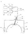
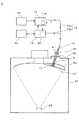
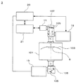
図1及び図2は、本発明に係る光学式膜厚計及び薄膜形成装置を示すもので、図1は回転ドラム式ホルダを備える薄膜形成装置を上方から見た概略構成説明図、図2はドーム式ホルダを備える薄膜形成装置を側方から見た概略構成説明図である。
また、図3乃至図8は、本発明に係る光学式膜厚計に関するもので、図3は光軸に対する反射ミラー角度と測定光強度の関係を示すグラフ図、図4は基板の傾きと測定光の割合変化を示す説明図、図5は基板角度と測定光強度の関係を示すグラフ図、図6はBK−7基板の透過率測定結果を示すグラフ図、図7はIRカットフィルタの透過率測定結果を示すグラフ図、図8はSiO 2 単層成膜時の、波長520nmにおける光学膜厚の時間経過による光量変化の計算結果を示すグラフ図である。
1 and 2 show an optical film thickness meter and a thin film forming apparatus according to the present invention. FIG. 1 is a schematic configuration explanatory view of a thin film forming apparatus provided with a rotating drum holder from above, and FIG. It is schematic structure explanatory drawing which looked at the thin film forming apparatus provided with a dome-type holder from the side.
FIGS. 3 to 8 relate to the optical film thickness meter according to the present invention. FIG. 3 is a graph showing the relationship between the reflection mirror angle with respect to the optical axis and the measurement light intensity, and FIG. FIG. 5 is a graph showing the relationship between the substrate angle and the measured light intensity, FIG. 6 is a graph showing the transmittance measurement result of the BK-7 substrate, and FIG. 7 is the transmission through the IR cut filter. FIG. 8 is a graph showing the calculation result of the change in light quantity over time of the optical film thickness at a wavelength of 520 nm when the SiO 2 single layer is formed.
本発明に係る光学式膜厚計は、測定専用のモニタ基板を測定するものではなく、測定基板として実基板(製品)Sの膜厚を測定するもので、図1及び図2に示すように、光源もしくは投光手段としての投光器11と、導光手段としての光ファイバ13(13a,13b)と、球面アクロマティックレンズ15と、反射ミラー17と、受光手段としての受光器19と、を有して構成されている。また、投光器11には、光源用安定化電源21を介して電圧が印加され、受光器19はコンピュータ(演算用PC)23に接続されている。
なお、図4に示すように、本明細書中においては、反射ミラー17により反射される前の測定光を出射光L1、反射された後の測定光を反射光L2(L2−1、L2−2、L2−3)と区別して記載している。
The optical film thickness meter according to the present invention does not measure a monitor substrate dedicated to measurement, but measures the film thickness of an actual substrate (product) S as a measurement substrate, as shown in FIG. 1 and FIG. A
As shown in FIG. 4, in this specification, the measurement light before being reflected by the
投光器11は、測定に用いる出射光L1を出力する装置であり、Ref回路11aが組み込まれており、また投光器11には光源用安定化電源21から電力が供給され、任意の波長を有する測定光を出射光側の光ファイバ13aに出射するように構成されている。
受光器19は、出射光L1によって測定基板である実基板Sを透過した光が、反射ミラー17で反射されて実基板Sを再び透過した反射光L2が反射光側の光ファイバ13bを介して入力される装置である。
受光器19は、光検出手段としての分光器20を備えており、測定光の波長や透過率の測定を行うことができ、また、分光器20による分析結果に基づいて光学薄膜の膜厚や光学特性を算出及び表示するためのコンピュータ(演算用PC)23に接続されている。
The
In the
The
光ファイバ13は、出射光側の光ファイバ13aと反射光側の光ファイバ13bからなる二分岐のバンドルファイバから構成され、ステンレス製の二分岐のフレキシブルチューブ内にまとめられている。出射光側の光ファイバ13aは、一端部側を投光器11に接続され、反射光側の光ファイバ13bは、一端部側を受光器19に接続されている。出射光側の光ファイバ13a及び反射光側の光ファイバ13bのそれぞれの光ファイバ端部14は、1つの束にまとめられ、光軸を球面アクロマティックレンズ15と測定基板である実基板Sに向けて配設されている。光ファイバ端部14から照射される出射光L1は、直径5〜6mm程度の円形断面とされている。
The
球面アクロマティックレンズ15は、波長による収差(色収差)と球面収差を除去するためのレンズであり、測定精度の向上を図ることができるもので、光ファイバ端部14と、薄膜形成装置1,2に形成された測定窓25の間に配設されている。
The spherical
反射ミラー17は、実基板Sの裏側に配設されており、実基板Sを透過した投光器11からの出射光L1を反射するものである。反射ミラー17は、Al膜、Ag膜をコーティングしたミラーや、これらAl膜やAg膜上にMgF 2 又はSiOをオーバーコートしたミラー、また、その他の誘電体膜をオーバーコートしたミラーを用いることができる。反射面のサイズは任意であるが、実基板Sのサイズと同等程度とされることが望ましく、数cm程度である。反射ミラー17の反射面は80%程度の反射率を有している。反射ミラー17は、実基板Sに照射される出射光L1の光軸に対してほぼ垂直(直角)に配設されているため、出射光L1を反射して反射光L2とし、出射光L1の光軸と同経路で反射光L2が実基板Sを透過する。
なお、球面アクロマティックレンズ15と実基板Sと反射ミラー17は、光ファイバ端部14からの測定光の光軸に沿って配設されている。
The
The spherical
実基板Sとしては、ガラス等の材料で形成された部材を用いると好適である。本実施形態では、実基板Sとして板状のものを用いているが、実基板Sの形状としてはこのような板状のものに限定されない。また、表面に薄膜を形成できる他の形状、例えばレンズ形状、円筒状、円環状といった形状であってもよい。ここで、ガラス材料とは、二酸化ケイ素(SiO 2 )で形成された材料であり、具体的には、石英ガラス、ソーダ石灰ガラス、ホウケイ酸ガラスなどが挙げられる。なお、本実施形態において実基板Sとは、光学フィルタFも含むものとしている。 As the actual substrate S, it is preferable to use a member formed of a material such as glass. In the present embodiment, a plate-shaped substrate is used as the actual substrate S, but the shape of the actual substrate S is not limited to such a plate-shaped substrate. Moreover, the shape which can form a thin film on the surface, for example, shapes, such as a lens shape, cylindrical shape, and a ring shape, may be sufficient. Here, the glass material is a material formed of silicon dioxide (SiO 2 ), and specifically includes quartz glass, soda-lime glass, borosilicate glass, and the like. In the present embodiment, the actual substrate S includes the optical filter F.
また、実基板Sの材料はガラスに限定されず、プラスチック樹脂などであってもよい。プラスチック樹脂の例としては、例えばポリカーボネート、ポリエチレンテレフタレート、ポリブチレンテレフタレート、アクリルニトリル−ブタジエン−スチレン共重合体、ナイロン、ポリカーボネート−ポリエチレンテレフタレート共重合体、ポリカーボネート−ポリブチレンテレフタレート共重合体、アクリル、ポリスチレン、ポリエチレン、ポリプロピレンからなる群より選択される樹脂材料、またはこれらの材料とガラス繊維及び/またはカーボン繊維との混合物などが挙げられる。 The material of the actual substrate S is not limited to glass, and may be a plastic resin or the like. Examples of the plastic resin include, for example, polycarbonate, polyethylene terephthalate, polybutylene terephthalate, acrylonitrile-butadiene-styrene copolymer, nylon, polycarbonate-polyethylene terephthalate copolymer, polycarbonate-polybutylene terephthalate copolymer, acrylic, polystyrene, Examples thereof include resin materials selected from the group consisting of polyethylene and polypropylene, or mixtures of these materials with glass fibers and / or carbon fibers.
ここで、投光器11から出射された測定光(出射光L1及び反射光L2)が受光器19に入力されるまでの経路について説明する。
投光器11から出力された測定光である出射光L1は、投光側の光ファイバ13aを介して光ファイバ端部14から球面アクロマティックレンズ15に照射され、薄膜形成装置1,2に形成された測定窓25を通過して、実基板Sに照射される。
Here, a path until the measurement light (emitted light L1 and reflected light L2) emitted from the
The outgoing light L1, which is the measurement light output from the
実基板Sに照射された出射光L1は、実基板Sを透過して、その実基板Sの裏側に配設された反射ミラー17により反射され反射光L2となる。反射ミラー17によって反射された反射光L2は、再び実基板S、測定窓25、球面アクロマティックレンズ15を透過して光ファイバ端部14に至る。そして、実基板S側からの測定光(反射光L2)のみが反射光側の光ファイバ13bを通過して、受光器19に導かれる。
なお、後述するように、実基板Sは、測定光の光軸に対して傾き角度を有するように配設されている。
The outgoing light L1 irradiated to the actual substrate S is transmitted through the actual substrate S, reflected by the
As will be described later, the actual substrate S is disposed so as to have an inclination angle with respect to the optical axis of the measurement light.
次に、薄膜形成装置1,2への光学式膜厚計の取り付け状態について説明する。
図1に示した薄膜形成装置1は、回転ドラム式ホルダ33を備えるスパッタ(マグネトロンスパッタ)装置であり、真空容器31と、実基板Sが取り付けられる基板ホルダとしての回転ドラム式ホルダ33と、回転ドラム式ホルダ33の外側に対向して設けられたスパッタ手段35と、不図示のスパッタガス供給手段と、を少なくとも有して構成されている。
Next, the attachment state of the optical film thickness meter to the thin
The thin
真空容器31は、公知の薄膜形成装置で通常用いられるようなステンレススチール製で、ほぼ直方体形状をした中空体である。また、真空容器31の側面側、すなわち真空容器31の回転ドラム式ホルダ33の径方向側には測定窓25が形成されている。
回転ドラム式ホルダ33は、略円筒状に形成され、回転軸を真空容器31の上下方向に向けて配置されている。回転ドラム式ホルダ33は、実基板Sの保持手段としての機能を有しており、実基板Sはこの回転ドラム式ホルダ33の外周面に不図示の基板ホルダなどを介して並べて取り付けられる。
The
The
回転ドラム式ホルダ33の実基板Sが取り付けられる部分には所定サイズの開口部(不図示)が形成されているため、実基板Sを透過した測定光は回転ドラム式ホルダ33の内側に入射することができる。なお、回転ドラム式ホルダ33は、中空角柱状に形成されてもよい。
スパッタ手段35は、一対のターゲットと、ターゲットを保持する一対のマグネトロンスパッタ電極と、電源装置と(いずれも不図示)、により構成される。ターゲットの形状は平板状であり、ターゲットの長手方向が回転ドラム式ホルダ33の回転軸線と平行になるように設置されている。
Since the opening (not shown) of a predetermined size is formed in the portion where the actual substrate S of the
The sputtering means 35 includes a pair of targets, a pair of magnetron sputtering electrodes that hold the targets, and a power supply device (both not shown). The target has a flat plate shape and is installed so that the longitudinal direction of the target is parallel to the rotation axis of the
スパッタ手段35の周辺にはアルゴン等のスパッタガスを供給するスパッタガス供給手段が設けられている。ターゲットの周辺が不活性ガス雰囲気になった状態で、マグネトロンスパッタ電極に電源から交流電圧が印加されると、ターゲット周辺のスパッタガスの一部は電子を放出してイオン化する。このイオンが加速され、ターゲットに衝突することでターゲットの表面の原子や粒子(ターゲットがニオブの場合はニオブ原子やニオブ粒子)が叩き出される。このニオブ原子やニオブ粒子は薄膜の原料である膜原料物質(蒸着物質)であり、実基板Sの表面に付着して薄膜が形成される。 A sputtering gas supply means for supplying a sputtering gas such as argon is provided around the sputtering means 35. When an AC voltage is applied from the power source to the magnetron sputtering electrode in a state where the periphery of the target is in an inert gas atmosphere, a part of the sputtering gas around the target emits electrons and is ionized. When the ions are accelerated and collide with the target, atoms and particles on the surface of the target (if the target is niobium, niobium atoms and niobium particles) are knocked out. The niobium atoms and niobium particles are film raw material (vapor deposition material) that is a raw material of the thin film, and adhere to the surface of the actual substrate S to form a thin film.
薄膜形成装置1では、回転ドラム式ホルダ33が回転すると、回転ドラム式ホルダ33の外周面に保持された実基板Sが公転して、スパッタ手段35に面する2カ所の位置を繰り返し移動することになる。そして、このように実基板Sが公転することで、スパッタ手段35でのスパッタ処理が順次繰り返し行われて、実基板Sの表面に薄膜が形成される。
In the thin
なお、薄膜形成装置1にプラズマ発生手段を取り付けて、薄膜の形成と同時に、薄膜形成前の実基板Sの表面にプラズマ処理を行う前処理工程や薄膜形成後の実基板Sの表面にプラズマ処理を行う後処理工程を行う構成とすることができる。もちろん、スパッタ手段35に代えて他の成膜手段を用いる構成であってもよい。
In addition, the plasma generating means is attached to the thin
薄膜形成装置1において、本発明に係る光学式膜厚計は、真空容器31の一部に形成された測定窓25から出射光L1を実基板Sに向けて照射し、実基板Sの裏側に設置された反射ミラー17によって、実基板Sを透過した出射光L1が反射された反射光L2が、再び実基板Sを透過できるようになっている。
In the thin
具体的には、投光器11と受光器19とに接続された光ファイバ13の他端部と球面アクロマティックレンズ15は真空容器31の外側に配設されており、反射ミラー17は、実基板Sの裏側、且つ、回転ドラム式ホルダ33の内側位置に固定してある。実基板Sが取り付けられた位置の回転ドラム式ホルダ33には開口部が形成されているため、実基板Sを透過した出射光L1を、回転ドラム式ホルダ33の開口部を通過してその内側に配設された反射ミラー17で反射させることができる。
Specifically, the other end of the
このように、光学式膜厚計が取り付けられることによって、回転ドラム式ホルダ33に取り付けられた実基板Sの光学膜厚や光学特性などを成膜中でも測定をすることができる。具体的には、回転ドラム式ホルダ33を、実基板Sの測定部分が測定光の光軸に重なる所定位置で、膜厚などの測定を行うことになる。なお、実基板Sは、測定光の光軸に対して傾き角度を有するように配設されている。
薄膜形成装置1においては、反射ミラー17は実基板Sの裏側、且つ、回転ドラム式ホルダ33の内側位置に固定されている。このため、反射ミラー17の汚れが生じにくく、スパッタ中のプラズマ放電から迷光の影響も受け難いという利点がある。
Thus, by attaching the optical film thickness meter, the optical film thickness, optical characteristics, etc. of the actual substrate S attached to the
In the thin
また、反射ミラー17を複数の実基板Sに対して取付けてもよい。すなわち、実基板Sと反射ミラー17とをペアにして組み付けた場合、出射光L1の位置に対応した所定位置で、実基板Sの膜厚や光学特性について、各実基板Sの複数の測定を行なうことができる。このように構成することで、回転ドラム式ホルダ33を回転させて、所定位置に実基板Sを配置することにより、回転ドラム式ホルダ33に取り付けられた状態の複数の実基板Sに順次測定光を透過させて光学膜厚を測定することができる。このため、複数の実基板Sの膜厚を同時に測定することができ、より高い精度で光学膜厚の計測が可能な薄膜形成装置を得ることができる。
Further, the
つぎに、図2に示した薄膜形成装置2は、真空容器41内に配設された回転ホルダ43を備える蒸着装置であり、基板ホルダとして、実基板Sが取り付けられるドーム状の回転ホルダ43と、回転ホルダ43と対向して下方側に設けられた蒸着手段45と、を少なくとも有して構成されている。また、本実施形態における薄膜形成装置2では、回転ホルダ43と蒸着手段45の間の位置に、補正板47が配設されている。
真空容器41は、公知の薄膜形成装置で通常用いられるようなステンレススチール製で、ほぼ直方体形状をした中空体である。また、回転ホルダ43の上側面に測定窓25が形成されている。
Next, the thin
The
回転ホルダ43は、略ドーム状に形成され、回転軸を上下方向に向けて真空容器41内に配置され、基板保持手段としての機能を有しており、回転ホルダ43に複数の実基板Sを不図示の取り付け治具を介して装着することができる。回転ホルダ43の実基板Sが取り付けられる部分は所定サイズの開口部(不図示)が形成されている。
The
蒸着手段45は、真空容器41の下方側の回転ホルダ43に対向した位置に設置されており、例えば、るつぼに入れた蒸着物質と、蒸着物質を加熱するための電子ビーム源または高周波コイルなどとから構成されている。もちろん、蒸着手段として、ターゲットと電極と電源とで構成されるスパッタ源を用いてもよい。
The vapor deposition means 45 is installed at a position facing the
補正板47は、回転ホルダ43の取り付け位置により生じる実基板S上の膜厚の差を補正する略板状の部材であって、真空容器41側に固定されている。これにより、実基板Sに薄膜を形成する際、蒸着手段45から実基板Sに向かって蒸発する蒸発物質の堆積を部分的に妨げることによって膜厚を補正することができる。薄膜形成装置2では、蒸着手段45から蒸発した蒸発物質が、回転ホルダ43に取り付けられた実基板S上に堆積されることで成膜を行うものである。このとき、回転ホルダ43の回転と補正板47によって実基板Sの位置による膜厚の差を補正している。
The
薄膜形成装置2において、本発明に係る光学式膜厚計は、真空容器41の一部に形成された測定窓25から出射光L1を実基板Sに向けて照射し、実基板Sの下方側の補正板47に設置された反射ミラー17によって、実基板Sを透過した出射光L1を反射して反射光L2とし、再び実基板Sを透過するようにしている。
In the thin
具体的には、投光器11と受光器19とに接続された光ファイバ端部14と球面アクロマティックレンズ15は真空容器41の外側に配設されており、反射ミラー17は、実基板Sの下方側、且つ、補正板47の上側位置に固定してある。実基板Sが取り付けられた位置の回転ホルダ43には開口部が形成されているため、実基板Sを透過した出射光L1を、回転ホルダ43の開口部を通過してその下方側に配設された反射ミラー17によって反射させることができる。
Specifically, the
このように、光学式膜厚計が取り付けられることによって、回転ホルダ43に取り付けられた実基板Sの膜厚などの光学特性を成膜中でも測定をすることができる。具体的には、回転ホルダ43を、実基板Sの測定部分が測定光の光軸に重なる所定位置で、膜厚などの測定を行うことになる。
Thus, by attaching the optical film thickness meter, the optical characteristics such as the film thickness of the actual substrate S attached to the
なお、光学式膜厚計は、測定光の光軸に対して実基板Sが傾き角度を有するように配設されている。
また、補正板47の実基板S側に反射ミラー17が取り付けられるため、固定された状態で測定円周上に配設される実基板Sを測定することができるので、安定した測定が可能となる。
The optical film thickness meter is arranged so that the actual substrate S has an inclination angle with respect to the optical axis of the measurement light.
In addition, since the reflecting
薄膜形成装置2において、反射ミラー17は補正板47の実基板Sと同じ側に取り付けられており、蒸着手段45からの蒸着物質が回り込んで反射ミラー17の反射面に付着する可能性がある為、反射ミラー17の直前に回り込み防止ガラスを取り付けることができる。さらに、回り込み防止ガラスにも蒸着物質が付着しないように筒状のフードで囲んでもよい。
In the thin
なお、回り込み防止ガラスは定期的に交換すると好適である。また、回り込み防止ガラスも実基板Sと同様に測定光の光軸に対して角度を有して配設されるとさらに好適である。 Note that it is preferable to periodically replace the wraparound prevention glass. Further, it is more preferable that the wrap-around prevention glass is disposed at an angle with respect to the optical axis of the measurement light as with the actual substrate S.
また、薄膜形成装置1,2において、光学式膜厚計で測定をする際には、実基板Sを測定位置に正確に合わせる必要がある。そのため、薄膜形成装置1,2はいずれも、回転ドラム式ホルダ33若しくは回転ホルダ43を測定位置で止めるための回転制御手段を備えている。回転制御手段としては、公知の装置を適用することができ、例えば、位置センサと回転角度を常時監視及び制御することが可能なモータとを備えて構成することができる。
Further, in the thin
薄膜形成装置1,2では、測定窓25も測定光の光軸に対して所定の角度を有して配設されている。これは、実基板Sを所定角度傾けて配設することと同じ理由によるものである。このため、測定窓25のガラス部材によって反射する光線についても、受光器19側に入力されることを防いでいる。
In the thin
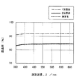
以下に、図3乃至図8に基づいて、本発明の光学式膜厚計について説明する。
なお、以下に示す測定若しくは計算例は、本発明に係る光学式膜計を取り付けた薄膜形成装置1における結果であるが、測定結果から導き出せる効果等はそのまま薄膜形成装置2にも適用できるものである。
Hereinafter, the optical film thickness meter of the present invention will be described with reference to FIGS.
In addition, although the measurement or calculation example shown below is a result in the thin
図3は、光軸に対する反射ミラー角度θと測定光強度の関係を示すグラフ図であり、反射ミラー角度が−6〜+6°までの測定結果である。
ここで、反射ミラー17の反射ミラー角度θは、反射ミラー17の反射面に対する垂線、測定光の光軸とのなす角度である。
図3で判明するように、反射ミラー17の角度θが0°において反射光の光量が最大値となる。なお、図3において、反射ミラー17の反射率は100%として換算したデータを示した。
FIG. 3 is a graph showing the relationship between the reflection mirror angle θ with respect to the optical axis and the measurement light intensity, and shows the measurement results when the reflection mirror angle is −6 to + 6 °.
Here, the reflection mirror angle θ of the
As can be seen from FIG. 3, when the angle θ of the
また、反射光の測定光強度は反射ミラー角度θが0°で最大となるものの、反射ミラー角度θが±1.0°において、反射ミラー角度θ=0°に比して、82〜87%以上の測定光強度を有しており、反射ミラー角度θが±0.6°の場合には、94〜96%以上の測定光強度を有している。なお、図3において、反射光の光量は、出射光L1の光量に対する、反射ミラー17において測定された光量(反射光L2の光量)の割合をパーセントで示した値である。 Further, the measurement light intensity of the reflected light becomes maximum when the reflection mirror angle θ is 0 °, but when the reflection mirror angle θ is ± 1.0 °, it is 82 to 87% compared to the reflection mirror angle θ = 0 °. When the reflection light angle θ is ± 0.6 °, the measurement light intensity is 94 to 96% or more. In FIG. 3, the amount of reflected light is a value indicating the ratio of the amount of light measured by the reflection mirror 17 (the amount of light of the reflected light L2) to the amount of emitted light L1 as a percentage.
また、許容できる反射ミラー17の反射ミラー角度θ(=−5.0〜+5.0°)は、反射ミラー17と球面アクロマティックレンズ15若しくは光ファイバ端部14との距離に応じ、上記範囲において変化する値である。すなわち、反射ミラー17と球面アクロマティックレンズ15若しくは光ファイバ端部14との距離が長くなれば、許容できる反射ミラー17の反射ミラー角度θは狭くなる。
なお、薄膜形成装置1においては、反射ミラー17と球面アクロマティックレンズ15との間の距離は、60〜350mm程度である。
Further, the allowable reflection mirror angle θ (= −5.0 to + 5.0 ° ) of the
In the thin
図4は、基板の傾きと測定光の割合変化を示す説明図であり、実基板Sの傾きと測定光(出射光及び反射光)の経路と光の割合変化を示すもので、図4(a)は、実基板Sの傾き角度α=0°の場合(傾いていない場合)、図4(b)は実基板Sの傾き角度αが所定の値を有する場合である。ここで、実基板Sの傾き角度αは、実基板Sの成膜面に対する垂線と、測定光の光軸とのなす角度である。
なお、図4中の光量は、実基板Sを取り付けない状態で測定した光量を100%とした模式図である。また、ここでは反射ミラー17の反射率は80%としている。
FIG. 4 is an explanatory diagram showing the inclination of the substrate and the change in the ratio of the measurement light, and shows the inclination of the actual substrate S, the path of the measurement light (emitted light and reflected light), and the change in the ratio of the light. FIG. 4A shows the case where the inclination angle α of the actual substrate S is 0 ° (when it is not inclined), and FIG. 4B shows the case where the inclination angle α of the actual substrate S has a predetermined value. Here, the inclination angle α of the actual substrate S is an angle formed between the perpendicular to the film formation surface of the actual substrate S and the optical axis of the measurement light.
In addition, the light quantity in FIG. 4 is a schematic diagram in which the light quantity measured without attaching the actual substrate S is 100%. Here, the reflectance of the
まず、図4(a)に示した、基板Sの傾き角度α=0°での測定光の経路と光の割合変化について説明する。
真空容器31の測定窓25から入射された光(出射光L1)は、実基板Sを透過する。このとき、入射された光(出射光L1)の全光量を「100」とすると、実基板Sの両側の表面で、透過せずにそれぞれ4.25%ずつ反射される(合計光量8.5)。この光量8.5の光は、反射光L2−1として測定窓25から出射される。したがって、実基板Sを透過する光量は91.5となる。この透過された光量91.5の光は、実基板Sの裏側に配設された反射ミラー17によって反射される。この折り返し反射光は、再度実基板Sを透過する事になり、同様に、合計8.5%の反射率を考慮し、残りの91.5%が実基板Sを透過する。即ち、光量83.7(1回目の透過光91.5×反射ミラー17からの折り返しによる2回目の透過率91.5%)がL2−2として測定窓25から出射される。このとき、反射ミラー17の反射率を無視するのは、実基板Sの測定前に、実基板Sが無い(反射ミラー17の反射のみ)の状態で100%ベースライン測定を行う為である。
折り返し反射光が実基板Sを透過する際、実基板Sで反射された光量7.78(91.5×8.5%)が再度反射ミラー17によって反射する場合、光量6.22(7.78×反射ミラー反射率80%)が再度実基板Sへ向かう。この光量6.22の再反射光も同様に実基板Sでそれぞれ4.25%ずつ合計8.5%が反射され、光量5.69(6.22×91.5%)がL2−3として測定窓25から出射される。
すなわち、測定窓25から出射される光は、L2−1〜3であり、実基板Sの反射光も混在してしまう。
First, the path of the measurement light and the change in the ratio of the light at the inclination angle α = 0 ° of the substrate S shown in FIG. 4A will be described.
Light (emitted light L1) incident from the
When the reflected light passes through the real substrate S, the light amount 7.78 (91.5 × 8.5%) reflected by the real substrate S is reflected by the
That is, the light emitted from the
つまり、測光窓25から入射される光(出射光L1)は、
(1)反射光L2−1・・・8.5(実基板Sによる両面反射光)
(2)反射光L2−2・・・83.7(反射ミラー17の反射により2回実基板Sを透過する光)
(3)反射光L2−3・・・5.69(再度反射ミラー17の反射により実基板Sを透過する光)
に大別される(反射光L2−4以上の多重反射光は微小な為、このモデルでは無視する)。
したがって、測定窓25から入射された光(出射光L1)のうち、97.89(8.5+83.7+5.69)程度の光量となり、反射光L2として真空容器31の測定窓25に向かう。実基板の傾き角度が0°であることから、反射された光線が全て同一経路を通るためである。
That is, the light (emitted light L1) incident from the
(1) Reflected light L2-1 ... 8.5 (double-sided reflected light by actual substrate S)
(2) Reflected light L2-2 ... 83.7 (light transmitted through the actual substrate S twice by reflection of the reflecting mirror 17)
(3) Reflected light L2-3... 5.69 (light transmitted through the actual substrate S again by the reflection of the reflection mirror 17)
(Multiple reflected light exceeding the reflected light L2-4 is very small and is ignored in this model).
Therefore, the amount of light incident from the measurement window 25 (outgoing light L1) is about 97.89 (8.5 + 83.7 + 5.69) and travels toward the
つまり、実基板Sの傾斜角度が0°の場合では、受光器19に入力される光(反射光L2)のうち14.19(8.5+5.69)程度が、実基板Sの反射光という事になる。従って、実基板Sの傾斜角度を0°とすると、受光器19に入射される反射光L2に所望の経路以外を通った光線を一割以上含むことになり、これが測定誤差を生じる原因になる。
That is, when the inclination angle of the actual substrate S is 0 °, about 14.19 (8.5 + 5.69) of the light (reflected light L2) input to the
次に、図4(b)に示した、基板の傾き角度が所定の値を有する場合の測定光の経路と光の割合変化について説明する。
前記図4(a)と同様に、出射光L1及び反射光L2の透過、反射が生じるが、実基板Sが所定角度傾いているため、実基板Sの表面で反射された8.5%の光は、実基板Sの傾きに応じた方向に反射される。従って、実基板Sの傾斜角度が所定値以上であれば、実基板Sの表面で反射された光線は受光器19には向かないことになる。
また、反射ミラー17で反射された反射光L2のうち、実基板Sで反射される光も、実基板Sの傾きに応じた方向に反射され受光器19には向かわないことになる。
つまり、実基板Sを所定角度傾けた場合には、実基板Sを2回透過した光線(光量83.7)のみが受光器19に入力されることになる。従って、誤差が生じる原因が少なく、測定の高精度化が期待できる。
Next, the measurement light path and the change in the ratio of the light when the tilt angle of the substrate has a predetermined value shown in FIG. 4B will be described.
As in FIG. 4A, the outgoing light L1 and the reflected light L2 are transmitted and reflected. However, since the actual substrate S is inclined by a predetermined angle, 8.5% of the light reflected by the surface of the actual substrate S is 8.5%. The light is reflected in a direction according to the inclination of the actual substrate S. Therefore, if the inclination angle of the actual substrate S is equal to or greater than a predetermined value, the light beam reflected by the surface of the actual substrate S is not suitable for the
Of the reflected light L2 reflected by the reflecting
That is, when the actual substrate S is tilted by a predetermined angle, only the light beam (light quantity 83.7) transmitted through the actual substrate S twice is input to the
図5は基板角度と測定光強度の関係を示すグラフ図であり、実基板Sの傾き角度αと反射光の光量の関係の測定結果で、図5(a)は傾き角度αが−6〜+6°までの測定結果、図5(b)は、図5(a)の結果を傾き角度α=+3〜+5.5°について拡大した図である。なお、図5中の光量は、実基板Sを取り付けていない状態で測定したデータを基準としている。 FIG. 5 is a graph showing the relationship between the substrate angle and the measurement light intensity. The measurement result shows the relationship between the inclination angle α of the actual substrate S and the amount of reflected light. FIG. FIG. 5B is a graph obtained by enlarging the result of FIG. 5A with respect to the inclination angle α = + 3 to + 5.5 °. In addition, the light quantity in FIG. 5 is based on data measured in a state where the actual substrate S is not attached.
図5(a)で判明するように、実基板Sの傾き角度がないα=0°において反射光の光量が最大値となる。これは、図4(a)に説明したように実基板Sの表裏面で反射した光線も含んでいるためである。 As can be seen from FIG. 5A, the amount of reflected light reaches a maximum value when α = 0 ° where the actual substrate S does not have an inclination angle. This is because light rays reflected on the front and back surfaces of the actual substrate S are included as described with reference to FIG.
実基板Sの角度を傾けていくと、実基板Sの表面で反射された光線は実基板Sの傾きに応じた方向に反射されるため、実基板Sの傾き角度とともに受光器19で測定される光量が減少していく。そして、およそ傾き角度4.5°以上の領域では、光量はほぼ一定の値を示すようになった。これは、図4(b)に説明したように、実基板Sの表裏面で反射した光を受光器19で取り込まないようになるためである。
When the angle of the actual substrate S is tilted, the light beam reflected by the surface of the actual substrate S is reflected in a direction corresponding to the tilt of the actual substrate S, and thus is measured by the
図5(b)により、およそ傾き角度4.5°以上で一定の値を示すようになることから、実基板Sの傾き角度は4.5°以上に設定すると好適である。ここで、実基板Sがいずれの方向に傾いても同様な効果が得られることから、傾き角度は、測定光Sの光軸に直行する面に対する角度の絶対値である。 As shown in FIG. 5B, a constant value is obtained at an inclination angle of about 4.5 ° or more. Therefore, the inclination angle of the actual substrate S is preferably set to 4.5 ° or more. Here, since the same effect can be obtained regardless of which direction the actual substrate S is tilted, the tilt angle is an absolute value of an angle with respect to a plane perpendicular to the optical axis of the measurement light S.
すなわち、実基板Sの傾き角度は、±4.5°以上に設定されることが望ましい。
また、実基板Sの傾き角度は、光量が一定の値を示す範囲内で最小であることが好ましい。ここで、図5(b)によれば、傾き角度4.5°程度では僅かに光量変化に傾きが認められるものの、傾き角度=5°程度以上で光量の変化が見られなくなる。
That is, it is desirable that the inclination angle of the actual substrate S is set to ± 4.5 ° or more.
Moreover, it is preferable that the inclination angle of the actual substrate S is the smallest within a range in which the light amount shows a constant value. Here, according to FIG. 5B, although a slight change in the light amount is recognized at an inclination angle of about 4.5 °, no change in the light amount can be seen at an inclination angle of about 5 ° or more.
また、実基板Sの傾き角度は、実基板Sと反射ミラー17、若しくは、実基板Sと球面アクロマティックレンズ15若しくは光ファイバ端部14との距離に応じて変化する値である。例えば、実基板Sと球面アクロマティックレンズ15若しくは光ファイバ端部14との距離が長くなれば、許容できる実基板Sの傾き角度は小さな値になる。
The inclination angle of the actual substrate S is a value that changes according to the distance between the actual substrate S and the
上述のように、薄膜形成装置1においては、反射ミラー17と球面アクロマティックレンズ15との間の距離は、60〜350mm程度である。
As described above, in the thin
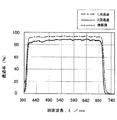
図6乃至図8は、本発明の光学式膜厚計による測定例であり、これらの図は、光学式膜厚計により実基板S(BK−7基板)や光学フィルタFを測定した結果であり、1回透過させて測定した結果と比較したものである。以下に説明するいずれの例においても、測定された実基板Sは傾き角度=5°として測定を行った。 6 to 8 are measurement examples using the optical film thickness meter of the present invention, and these figures are the results of measuring the actual substrate S (BK-7 substrate) and the optical filter F using the optical film thickness meter. Yes, and compared with the result measured once permeation. In any of the examples described below, the measured actual substrate S was measured with an inclination angle = 5 °.
(実施例1)
図6は、BK−7基板の透過率測定結果を示すグラフ図である。X軸は測定波長、Y軸は光量(透過率)である。図6では、本発明に係る光学式膜厚計による2回透過時の透過率測定結果と、分光光度計SolidSpec3700(島津製作所製)による1回透過時の透過率測定結果と、1回測定のデータを2回測定として換算した換算値を示している。
Example 1
FIG. 6 is a graph showing the transmittance measurement results of the BK-7 substrate. The X axis is the measurement wavelength, and the Y axis is the amount of light (transmittance). In FIG. 6, the transmittance measurement result at the time of two-time transmission by the optical film thickness meter according to the present invention, the transmittance measurement result at the time of one-time transmission by the spectrophotometer SolidSpec 3700 (manufactured by Shimadzu Corporation), and the one-time measurement The converted value obtained by converting the data as two measurements is shown.
図6から判明するように、BK−7基板は測定された全波長領域に渡りほぼフラットな透過率特性(光学特性)を有しており、2回透過の測定値と、1回透過を2回透過に換算した換算値とは、全波長域に渡りほぼ同じ値を示した。これは、本発明に係る光学式膜厚計は、真空容器31内に反射ミラー17を配置した簡単な構成でありながら、100%光量に対する変化量が大きい、すなわち、膜厚測定の制御精度を向上させることができる事を示している。
As can be seen from FIG. 6, the BK-7 substrate has almost flat transmittance characteristics (optical characteristics) over the entire measured wavelength range, and the measured value of the two-time transmission and the two-time transmission. The converted value converted to the double transmission showed almost the same value over the entire wavelength range. This is because the optical film thickness meter according to the present invention has a simple configuration in which the
(実施例2)
図7はIRカットフィルタの透過率測定結果を示すグラフ図である。IR(赤外線)カットフィルタは、BK−7基板上に、Nb 2 O 5 /SiO 2 を積層させた光学フィルタFである。図7においても、図6と同様に、X軸とY軸は、それぞれ測定波長と透過率を示しており、また、本発明に係る光学式膜厚計による測定結果(2回透過)と、分光光度計による測定(1回透過)と、1回透過のデータを2回透過に換算した(換算値)が示されている。
(Example 2)
FIG. 7 is a graph showing the transmittance measurement result of the IR cut filter. The IR (infrared) cut filter is an optical filter F in which Nb 2 O 5 / SiO 2 is laminated on a BK-7 substrate. In FIG. 7, as in FIG. 6, the X axis and the Y axis indicate the measurement wavelength and the transmittance, respectively, and the measurement result (double transmission) by the optical film thickness meter according to the present invention, A spectrophotometer measurement (one-time transmission) and a single-time transmission data converted into two-time transmission (converted value) are shown.
図7によれば、IRカットフィルタは、およそ700nm以上の赤外線波長域での透過率が0%近傍の値を示している。このIRカットフィルタの測定においても、2回透過の測定値と、1回透過を2回透過に換算した換算値とは、全波長域に渡りほぼ同じ値を示した。従って、IRカットフィルタの測定においても、本発明に係る光学式膜厚計は、従来の1回透過型の光学式膜厚計と少なくとも同等の測定精度を有していると言える。 According to FIG. 7, the IR cut filter has a value in the vicinity of 0% of transmittance in an infrared wavelength region of approximately 700 nm or more. Also in this IR cut filter measurement, the measured value of the two-time transmission and the converted value obtained by converting the one-time transmission into the two-time transmission showed substantially the same value over the entire wavelength range. Therefore, it can be said that the optical film thickness meter according to the present invention has at least the same measurement accuracy as the conventional single transmission optical film thickness meter in the measurement of the IR cut filter.
図8は、本発明の光学式膜厚計の特性を従来の測定法と比較したものであり、本発明に係る光学式膜厚計で計算した結果と、従来の1回透過で計算した結果とを比較した。計算(シミュレーション)には、市販の光学演算理論ソフトを用いた。 FIG. 8 compares the characteristics of the optical film thickness meter of the present invention with the conventional measurement method. The results calculated with the optical film thickness meter according to the present invention and the results calculated with the conventional one-time transmission are shown. And compared. For the calculation (simulation), commercially available optical calculation theory software was used.
(実施例3)
図8は、SiO 2 単層膜成膜時の、波長520nmにおける光学膜厚の時間経過による光量変化を示すグラフ図で、SiO 2 単層膜フィルタの光量変化計算結果であり、1回透過による計算結果と、本発明に係る光学式膜厚計によるSiO 2 単層膜フィルタの2回透過の計算結果と、を比較したものである。SiO 2 単層膜フィルタは、BK−7にSiO 2 単層膜を形成した光学フィルタFである。X軸は成膜時間(膜厚に比例)、Y軸は透過光量を示している。また、光量変化計算は、波長520nmの値である。
(Example 3)
8, when SiO 2 TansomakuNarumaku a graph illustrating a change of light intensity with time of the optical thickness at a wavelength of 520 nm, a light amount change calculation result of SiO 2 single-layer film filter, once transmission And the calculation result of the two-time transmission of the SiO 2 single layer film filter by the optical film thickness meter according to the present invention are compared. The SiO 2 single layer film filter is an optical filter F in which a SiO 2 single layer film is formed on BK-7. The X axis represents the film formation time (proportional to the film thickness), and the Y axis represents the amount of transmitted light. The light amount change calculation is a value at a wavelength of 520 nm.
図8で示すように、本発明に係る光学式膜厚計での2回透過の計算値(2回透過)と、1回透過の計算値(1回透過)とでは、本発明の2回透過の場合は、透過率及び透過光量ともに、変化量が大きくなっており、従来例に比して、この変化量が多い分だけ、測定精度が向上する。 As shown in FIG. 8, the calculated value of the two-time transmission (two-time transmission) and the calculated value of the one-time transmission (one-time transmission) in the optical film thickness meter according to the present invention are twice. In the case of transmission, the amount of change is large for both the transmittance and the amount of transmitted light, and the measurement accuracy is improved by the amount of the amount of change compared to the conventional example.
図8において、本発明に係る光学式膜厚計による測定値の計算結果と、1回透過による測定値の計算結果と、を比較すると、本発明の光学式膜厚計による測定の変化率の方が高いことがわかる。変化量の差はおよそ1.6乃至1.8倍であった。これは、実基板Sを2回透過することによる透過率の減少により変化量が大きくなるためである。測定値の変化量が大きいため、測定精度の向上を図ることができ、本発明に係る光学式膜厚計は、従来の1回透過型の光学式膜厚計よりも優れた測定精度を有していると言える。 In FIG. 8, when the calculation result of the measurement value by the optical film thickness meter according to the present invention is compared with the calculation result of the measurement value by single transmission, the change rate of the measurement by the optical film thickness meter of the present invention is You can see that it is higher. The difference in change amount was approximately 1.6 to 1.8 times. This is because the amount of change increases due to a decrease in the transmittance due to passing through the actual substrate S twice. Since the amount of change in the measured value is large, the measurement accuracy can be improved, and the optical film thickness meter according to the present invention has a measurement accuracy superior to that of the conventional single transmission type optical film thickness meter. I can say that.
S 実基板(測定基板)
F 光学フィルタ
L1 出射光
L2(L2−1,L2−2,L2−3) 反射光
1,2,3 薄膜形成装置
11 投光器
11a Ref回路
13 光ファイバ
13a 出射光側の光ファイバ
13b 反射光側の光ファイバ
14 光ファイバ端部
15 球面アクロマティックレンズ
17 反射ミラー
19 受光器
20 分光器
21 光源用安定化電源
23 コンピュータ(演算用PC)
25 測定窓
31,41,101 真空容器
33 回転ドラム式ホルダ
35 スパッタ手段
43,103 回転ホルダ
45 蒸着手段
47 補正板
105 ミラー
107 ミラーボックス
S Real board (measurement board)
F Optical filter L1 Emission light L2 (L2-1, L2-2, L2-3)
25
Claims (10)
前記実基板に向けて前記測定光としての出射光を出射する投光手段と、
前記実基板を介して前記投光手段と反対側の位置で、前記出射光を反射する反射ミラーと、
前記測定光を受光する受光手段と、
該受光手段により受光された前記測定光を検出する光検出手段と、を備え、
前記実基板の成膜面に対する垂線が前記測定光の光軸に対して所定角度を有して配設されることにより、前記受光手段は、前記実基板を透過し、且つ前記反射ミラーで反射して前記実基板を透過した前記測定光のみを受光することを特徴とする光学式膜厚計。 An optical film thickness meter that measures the optical film thickness by transmitting measurement light through an actual substrate,
Projection means for emitting outgoing light as the measurement light toward the actual substrate;
A reflecting mirror that reflects the emitted light at a position opposite to the light projecting means through the actual substrate ;
And a light-receiving means for receiving the pre-Symbol measuring light,
A light detecting means for detecting the measurement light received by the light receiving means,
The Rukoto normal to the film forming surface of the actual substrate is disposed with a predetermined angle with respect to the optical axis of the measurement light, the light receiving means is transmitted through the actual substrate, and reflected by the reflection mirror optical film thickness meter, characterized that you receive only the measurement light having passed through the actual substrate and.
蒸着材料を蒸発させる蒸着手段と前記基板ホルダとの間の位置に、前記真空容器側に固定されて配設される補正板と、
前記基板ホルダに前記実基板を取り付けた状態で、前記実基板に測定光を透過させて光学膜厚を測定する光学式膜厚計と、を備えた薄膜形成装置であって、
前記光学式膜厚計は、
請求項1乃至6のいずれか一項に記載の光学式膜厚計を用いたことを特徴とする光学式膜厚計を備えた薄膜形成装置。 A dome-shaped substrate holder that supports and rotates a real substrate in a vacuum vessel;
A correction plate disposed on the vacuum vessel side at a position between the vapor deposition means for evaporating the vapor deposition material and the substrate holder;
An optical film thickness meter for measuring an optical film thickness by transmitting measurement light to the actual substrate in a state where the actual substrate is attached to the substrate holder,
The optical film thickness meter is
A thin film forming apparatus comprising an optical film thickness meter, wherein the optical film thickness meter according to any one of claims 1 to 6 is used .
前記基板ホルダの外側に配設されたスパッタ手段と、
前記基板ホルダに前記実基板を取り付けた状態で、前記実基板に測定光を透過させて光学膜厚を測定する光学式膜厚計と、を備えた薄膜形成装置であって、
前記光学式膜厚計は、
請求項1乃至6のいずれか一項に記載の光学式膜厚計を用いたことを特徴とする光学式膜厚計を備えた薄膜形成装置。 A substantially cylindrical substrate holder that can rotate while supporting a real substrate in a vacuum vessel;
Sputtering means disposed outside the substrate holder;
An optical film thickness meter for measuring an optical film thickness by transmitting measurement light to the actual substrate in a state where the actual substrate is attached to the substrate holder,
The optical film thickness meter is
A thin film forming apparatus comprising an optical film thickness meter, wherein the optical film thickness meter according to any one of claims 1 to 6 is used .
Priority Applications (8)
| Application Number | Priority Date | Filing Date | Title |
|---|---|---|---|
| JP2009158798A JP4878632B2 (en) | 2009-07-03 | 2009-07-03 | Optical film thickness meter and thin film forming apparatus equipped with optical film thickness meter |
| EP10794137A EP2450662A1 (en) | 2009-07-03 | 2010-06-29 | Optical film thickness meter and thin film forming apparatus provided with optical film thickness meter |
| KR1020127002789A KR101317536B1 (en) | 2009-07-03 | 2010-06-29 | Optical film thickness meter and thin film forming apparatus provided with optical film thickness meter |
| US13/381,032 US8625111B2 (en) | 2009-07-03 | 2010-06-29 | Optical film thickness meter and thin film forming apparatus provided with optical film thickness meter |
| PCT/JP2010/061041 WO2011001968A1 (en) | 2009-07-03 | 2010-06-29 | Optical film thickness meter and thin film forming apparatus provided with optical film thickness meter |
| CN201080029355.3A CN102472611B (en) | 2009-07-03 | 2010-06-29 | Optical film thickness meter and thin film forming apparatus provided with optical film thickness meter |
| TW099121613A TWI404908B (en) | 2009-07-03 | 2010-07-01 | An optical film thickness gauge and a thin film forming apparatus having an optical film thickness gauge |
| HK12109090.6A HK1168417A1 (en) | 2009-07-03 | 2012-09-17 | Optical film thickness meter and thin film forming apparatus provided with optical film thickness meter |
Applications Claiming Priority (1)
| Application Number | Priority Date | Filing Date | Title |
|---|---|---|---|
| JP2009158798A JP4878632B2 (en) | 2009-07-03 | 2009-07-03 | Optical film thickness meter and thin film forming apparatus equipped with optical film thickness meter |
Publications (3)
| Publication Number | Publication Date |
|---|---|
| JP2011013145A JP2011013145A (en) | 2011-01-20 |
| JP2011013145A5 JP2011013145A5 (en) | 2011-04-28 |
| JP4878632B2 true JP4878632B2 (en) | 2012-02-15 |
Family
ID=43411040
Family Applications (1)
| Application Number | Title | Priority Date | Filing Date |
|---|---|---|---|
| JP2009158798A Active JP4878632B2 (en) | 2009-07-03 | 2009-07-03 | Optical film thickness meter and thin film forming apparatus equipped with optical film thickness meter |
Country Status (8)
| Country | Link |
|---|---|
| US (1) | US8625111B2 (en) |
| EP (1) | EP2450662A1 (en) |
| JP (1) | JP4878632B2 (en) |
| KR (1) | KR101317536B1 (en) |
| CN (1) | CN102472611B (en) |
| HK (1) | HK1168417A1 (en) |
| TW (1) | TWI404908B (en) |
| WO (1) | WO2011001968A1 (en) |
Families Citing this family (10)
| Publication number | Priority date | Publication date | Assignee | Title |
|---|---|---|---|---|
| EP2816317A4 (en) * | 2012-02-15 | 2015-10-14 | Shincron Co Ltd | Optical film thickness measurement apparatus and thin-film forming apparatus using optical film thickness measurement apparatus |
| JP5265050B1 (en) * | 2012-02-27 | 2013-08-14 | 株式会社シンクロン | LED light source device, film thickness measuring device, and thin film forming device |
| CN104395690B (en) * | 2012-06-13 | 2017-05-31 | 株式会社新柯隆 | Film thickness measurement device and film formation device |
| CN104350380B (en) * | 2012-09-10 | 2017-03-15 | 株式会社新柯隆 | Measurement apparatus and film formation device |
| CN105143500B (en) * | 2012-10-04 | 2017-10-10 | 康宁股份有限公司 | Optics painting method, equipment and product |
| KR101544968B1 (en) | 2013-07-05 | 2015-08-19 | 한국표준과학연구원 | Thickness Measuring Apparatus and Thickness Measuring Method |
| JP6800800B2 (en) * | 2017-04-06 | 2020-12-16 | 株式会社ニューフレアテクノロジー | Growth rate measuring device and growth rate detection method |
| JP6923344B2 (en) | 2017-04-13 | 2021-08-18 | 株式会社Screenホールディングス | Peripheral processing equipment and peripheral processing method |
| US11313670B2 (en) * | 2020-09-30 | 2022-04-26 | National Tsing Hua University | Inspection method for multilayer semiconductor device |
| CN115452337B (en) * | 2022-08-24 | 2023-04-07 | 东莞艾塔极新材料科技有限公司 | Size checkout stand that OCA optical film die-cutting processing was used |
Family Cites Families (13)
| Publication number | Priority date | Publication date | Assignee | Title |
|---|---|---|---|---|
| JPS5491263A (en) * | 1977-12-28 | 1979-07-19 | Ulvac Corp | Film thickness detector |
| JPS5644802A (en) * | 1979-09-20 | 1981-04-24 | Hideo Takada | System and method of measuring film thickness and coating varnish film thickness |
| JPS5972010A (en) | 1982-10-19 | 1984-04-23 | Ulvac Corp | Film thickness monitoring device of optical film forming device |
| JPH0611442A (en) * | 1992-06-29 | 1994-01-21 | Kurabo Ind Ltd | Infrared optical device |
| US7304744B1 (en) | 1998-12-24 | 2007-12-04 | Sharp Kabushiki Kaisha | Apparatus and method for measuring the thickness of a thin film via the intensity of reflected light |
| DE60233931D1 (en) * | 2001-02-07 | 2009-11-19 | Asahi Glass Co Ltd | METHOD FOR PRODUCING A SPUTTER FILM |
| JP3737409B2 (en) * | 2001-10-15 | 2006-01-18 | 日本電信電話株式会社 | Film thickness monitoring apparatus and method |
| JP2004219108A (en) * | 2003-01-09 | 2004-08-05 | Dainippon Printing Co Ltd | Method and apparatus for inspecting irregularities in film thickness of colored film |
| JP4547489B2 (en) * | 2003-05-01 | 2010-09-22 | 株式会社昭和真空 | Optical thin film forming apparatus equipped with film thickness measuring device and optical thin film forming method |
| JP2005301032A (en) * | 2004-04-14 | 2005-10-27 | Olympus Corp | Optical thin film forming apparatus, optical thin film forming method and optical element |
| TWI252301B (en) * | 2004-07-30 | 2006-04-01 | Delta Electronics Inc | Deposition system and film thickness monitoring device thereof |
| JP2006214935A (en) | 2005-02-04 | 2006-08-17 | Omron Corp | Inspection device of thin film, and inspection method of the thin film |
| JP4792242B2 (en) * | 2005-05-27 | 2011-10-12 | オリンパス株式会社 | Thin film forming apparatus and thin film forming method |
-
2009
- 2009-07-03 JP JP2009158798A patent/JP4878632B2/en active Active
-
2010
- 2010-06-29 WO PCT/JP2010/061041 patent/WO2011001968A1/en active Application Filing
- 2010-06-29 KR KR1020127002789A patent/KR101317536B1/en active IP Right Grant
- 2010-06-29 US US13/381,032 patent/US8625111B2/en active Active
- 2010-06-29 EP EP10794137A patent/EP2450662A1/en not_active Withdrawn
- 2010-06-29 CN CN201080029355.3A patent/CN102472611B/en active Active
- 2010-07-01 TW TW099121613A patent/TWI404908B/en active
-
2012
- 2012-09-17 HK HK12109090.6A patent/HK1168417A1/en not_active IP Right Cessation
Also Published As
| Publication number | Publication date |
|---|---|
| KR20120052270A (en) | 2012-05-23 |
| CN102472611B (en) | 2015-06-17 |
| HK1168417A1 (en) | 2012-12-28 |
| CN102472611A (en) | 2012-05-23 |
| EP2450662A1 (en) | 2012-05-09 |
| JP2011013145A (en) | 2011-01-20 |
| WO2011001968A1 (en) | 2011-01-06 |
| KR101317536B1 (en) | 2013-10-15 |
| TWI404908B (en) | 2013-08-11 |
| US8625111B2 (en) | 2014-01-07 |
| TW201109617A (en) | 2011-03-16 |
| US20120105872A1 (en) | 2012-05-03 |
Similar Documents
| Publication | Publication Date | Title |
|---|---|---|
| JP4878632B2 (en) | Optical film thickness meter and thin film forming apparatus equipped with optical film thickness meter | |
| US7345765B2 (en) | Optical monitoring of thin films using fiber optics | |
| JP2011013145A5 (en) | ||
| JP5319856B1 (en) | Film thickness measuring apparatus and film forming apparatus | |
| JPH11241162A (en) | Sputtering method capable of optically monitoring and device therefor | |
| JP5265050B1 (en) | LED light source device, film thickness measuring device, and thin film forming device | |
| WO2015004755A1 (en) | Optical film thickness measurement device, thin film forming device, and method for measuring film thickness | |
| JP4732569B2 (en) | Method for continuously determining the optical layer thickness of a coating | |
| JPH11162954A (en) | Method and equipment for measuring thin film by optical means and film formation equipment | |
| JP7240321B2 (en) | Methods of assembling optical systems and minimizing distortion due to retardance in optical assemblies | |
| JP4049458B2 (en) | Thin film thickness measuring apparatus and thin film thickness measuring method | |
| US7626169B1 (en) | Optical reference, and a method of using same | |
| Zoeller et al. | Direct optical monitoring enables high performance applications in mass production | |
| JP2006337303A (en) | Apparatus for measuring humidity in vacuum chamber | |
| JP2012219281A (en) | Film deposition apparatus | |
| JP2011074434A (en) | Film deposition method and film deposition system | |
| JPH09143743A (en) | Plasma cvd apparatus | |
| WO2016031360A1 (en) | Surface plasmon detection device and surface plasmon detection method | |
| JP2004052088A (en) | Physical vapor deposition film deposition apparatus | |
| JPH03206906A (en) | Optical film-thickness monitor |
Legal Events
| Date | Code | Title | Description |
|---|---|---|---|
| A521 | Request for written amendment filed |
Free format text: JAPANESE INTERMEDIATE CODE: A523 Effective date: 20110308 |
|
| A621 | Written request for application examination |
Free format text: JAPANESE INTERMEDIATE CODE: A621 Effective date: 20110308 |
|
| A871 | Explanation of circumstances concerning accelerated examination |
Free format text: JAPANESE INTERMEDIATE CODE: A871 Effective date: 20110308 |
|
| A975 | Report on accelerated examination |
Free format text: JAPANESE INTERMEDIATE CODE: A971005 Effective date: 20110330 |
|
| A131 | Notification of reasons for refusal |
Free format text: JAPANESE INTERMEDIATE CODE: A131 Effective date: 20110419 |
|
| A521 | Request for written amendment filed |
Free format text: JAPANESE INTERMEDIATE CODE: A523 Effective date: 20110617 |
|
| A131 | Notification of reasons for refusal |
Free format text: JAPANESE INTERMEDIATE CODE: A131 Effective date: 20110906 |
|
| A521 | Request for written amendment filed |
Free format text: JAPANESE INTERMEDIATE CODE: A523 Effective date: 20111004 |
|
| TRDD | Decision of grant or rejection written | ||
| A01 | Written decision to grant a patent or to grant a registration (utility model) |
Free format text: JAPANESE INTERMEDIATE CODE: A01 Effective date: 20111122 |
|
| A01 | Written decision to grant a patent or to grant a registration (utility model) |
Free format text: JAPANESE INTERMEDIATE CODE: A01 |
|
| A61 | First payment of annual fees (during grant procedure) |
Free format text: JAPANESE INTERMEDIATE CODE: A61 Effective date: 20111128 |
|
| R150 | Certificate of patent or registration of utility model |
Ref document number: 4878632 Country of ref document: JP Free format text: JAPANESE INTERMEDIATE CODE: R150 Free format text: JAPANESE INTERMEDIATE CODE: R150 |
|
| FPAY | Renewal fee payment (event date is renewal date of database) |
Free format text: PAYMENT UNTIL: 20141209 Year of fee payment: 3 |
|
| R250 | Receipt of annual fees |
Free format text: JAPANESE INTERMEDIATE CODE: R250 |
|
| R250 | Receipt of annual fees |
Free format text: JAPANESE INTERMEDIATE CODE: R250 |
|
| R250 | Receipt of annual fees |
Free format text: JAPANESE INTERMEDIATE CODE: R250 |
|
| R250 | Receipt of annual fees |
Free format text: JAPANESE INTERMEDIATE CODE: R250 |
|
| R250 | Receipt of annual fees |
Free format text: JAPANESE INTERMEDIATE CODE: R250 |
|
| R250 | Receipt of annual fees |
Free format text: JAPANESE INTERMEDIATE CODE: R250 |
|
| R250 | Receipt of annual fees |
Free format text: JAPANESE INTERMEDIATE CODE: R250 |
|
| R250 | Receipt of annual fees |
Free format text: JAPANESE INTERMEDIATE CODE: R250 |