JP4816553B2 - Printed circuit board mounting base - Google Patents
Printed circuit board mounting base Download PDFInfo
- Publication number
- JP4816553B2 JP4816553B2 JP2007104769A JP2007104769A JP4816553B2 JP 4816553 B2 JP4816553 B2 JP 4816553B2 JP 2007104769 A JP2007104769 A JP 2007104769A JP 2007104769 A JP2007104769 A JP 2007104769A JP 4816553 B2 JP4816553 B2 JP 4816553B2
- Authority
- JP
- Japan
- Prior art keywords
- printed wiring
- pin
- wiring board
- support pin
- magnet
- Prior art date
- Legal status (The legal status is an assumption and is not a legal conclusion. Google has not performed a legal analysis and makes no representation as to the accuracy of the status listed.)
- Active
Links
Images


Landscapes
- Electric Connection Of Electric Components To Printed Circuits (AREA)
Description
本発明は、プリント配線基板を熱処理する際に、プリント配線基板に反りが発生しないようにしたプリント配線基板取り付け台に関するものである。 The present invention relates to a printed wiring board mounting base that prevents the printed wiring board from warping when heat-treating the printed wiring board.
近年、電子部品をプリント配線基板に半田付けする際にリフロー半田付け装置が使用されている。リフロー半田付け装置は、プリント配線基板に予め半田ペーストを塗布し、その上に電子部品を載せてプリント配線基板を加熱することで、その半田を溶解させ半田付けを行う装置である。一般的にプリント配線基板材料として使用されるガラスエポキシ材の軟化温度は約120℃前後であるために、リフロー半田付け装置での加熱の際に、搭載された部品の自重等で反りが発生してしまう。さらに、昨今、無鉛半田が使用され、一般的な無鉛半田は、鉛入り半田に比べ、融点が高く、リフロー半田付け工程において、リフロー半田付け装置内のヒータ設定温度が高くなることにより、プリント配線基板の反りをより促進する傾向にある。 In recent years, a reflow soldering apparatus is used when an electronic component is soldered to a printed wiring board. The reflow soldering apparatus is an apparatus for applying solder paste to a printed wiring board in advance, placing an electronic component thereon, and heating the printed wiring board to melt the solder and perform soldering. Generally, the glass epoxy material used as a printed wiring board material has a softening temperature of about 120 ° C., so when heated by a reflow soldering device, warpage occurs due to the weight of the mounted components. End up. In addition, lead-free solder is used in recent years, and general lead-free solder has a higher melting point than lead-containing solder, and in the reflow soldering process, the heater set temperature in the reflow soldering device becomes higher. There is a tendency to further promote the warpage of the substrate.
以下に従来のリフロー半田付けの際のプリント配線基板の反り防止のためのプリント配線基板取り付け台について説明する。 A conventional printed wiring board mounting base for preventing warpage of the printed wiring board during reflow soldering will be described below.
従来、プリント配線基板の反り防止のためのプリント配線基板取り付け台は特許文献1に記載されたものが知られている。 2. Description of the Related Art Conventionally, a printed wiring board mounting base for preventing warpage of a printed wiring board is described in Patent Document 1.
従来のプリント配線基板取り付け台を図11に示す。 The printed circuit board mounting for traditional shown in FIG. 11.
1は熱処理するプリント配線基板であり、2はプリント配線基板1を固定するためのマグネットである。3はプリント配線基板1を載置し支持するための平板であり、4は平板3に複数のマグネット2を内蔵している反り防止用治具である。5は反り防止用治具4に内蔵されたマグネット2に対応した位置のプリント配線基板1上に載置され、プリント配線基板を固定するためのマグネットである。
Reference numeral 1 denotes a printed wiring board to be heat-treated, and 2 denotes a magnet for fixing the printed wiring board 1. 3 is a flat plate for mounting and supporting the printed wiring board 1, and 4 is a warpage prevention jig in which a plurality of
以上のように構成された従来のプリント配線基板取り付け台について、以下その動作について説明する。 The operation of the conventional printed wiring board mounting base configured as described above will be described below.
反り防止用治具4にプリント配線基板1を重ね合わせ、マグネット5を反り防止用治具に内蔵されたマグネット2に対応した位置のプリント配線基板1上に載置する。反り防止用治具4に埋め込まれたマグネット2とプリント配線基板1上のマグネット5との間の引力によってプリント配線基板1を反り防止用治具4に固定することで、プリント配線基板1に反りが発生するのを防止する。
しかしながら上記の従来の構成では、マグネット2とマグネット5が直接接触していないので、プリント配線基板を挟み込む力が弱いという問題点を有していた。
However, since the
また、マグネットと電子部品との間の距離が近いため、実装される電子部品が半田が溶融している状態ではマグネットの磁力に引き寄せられて実装位置がずれるという問題点を有していた。 Further, since the distance between the magnet and the electronic component is short, there is a problem that the mounting position is shifted due to the magnetic force of the magnet when the electronic component to be mounted is melted in the solder.
また、プリント配線基板の反り防止治具が平板であったため、両面実装ができないという問題点を有していた。 In addition, since the printed wiring board warpage prevention jig is a flat plate, it has a problem that it cannot be mounted on both sides.
本発明は上記従来の問題点を解決するもので、プリント配線基板を固定する力が強く、実装される電子部品がマグネットの磁気の影響を受けず、両面実装にも対応できるプリント配線基板の反りを防止するプリント配線基板取り付け台を提供することを目的とする。 The present invention is intended to solve the above problems, strong force of fixing the printed circuit board is, electronic components mounted is not subjected to magnetic influence of the magnet, the printed wiring board which can cope with double-sided mounting An object of the present invention is to provide a printed wiring board mounting base that prevents warping.
本発明は、高温の炉内で電子部品を半田付けするプリント配線基板を支持するプリント配線基板取り付け台であって、プリント配線基板に設けた基板穴と、筒部の先端から内部に設けた空洞の底部にマグネットを配置したサポートピンAと、磁性材料からなり、頭部とその頭部よりも小径のピン部からなる押えピンとを備え、前記サポートピンAの筒部の先端に前記プリント配線基板を載置した状態で、そのプリント配線基板の基板穴から前記押えピンのピン部を前記サポートピンAの空洞に挿入し、前記空洞の底部に配置されたマグネットに前記押えピンのピン部を接触させることによりその接触磁力でプリント配線基板をサポートピンAと押えピンにより取り付けるようにしたものであり、プリント配線基板を上下から接触磁力で固定し、熱処理時にプリント配線基板の反りの発生を防止することができるとともに、表裏両面に電子部品を実装する両面実装のプリント配線基板の取り付けにも適応できるという作用を有する。 The present invention is a printed wiring board mounting base for supporting a printed wiring board for soldering electronic components in a high-temperature furnace, and includes a board hole provided in the printed wiring board and a cavity provided inside from the tip of a cylindrical portion. A support pin A having a magnet disposed on the bottom of the printed circuit board, and a press pin made of a magnetic material and having a head and a pin having a smaller diameter than the head, and the printed wiring board at the tip of the cylindrical portion of the support pin A Is inserted into the cavity of the support pin A from the board hole of the printed wiring board, and the pin part of the presser pin is brought into contact with the magnet disposed at the bottom of the cavity. It is obtained by the printed circuit board with the contact force to attach the support pin a and the pressing pin by and fixed in a contact force of the printed circuit board from above and below It is possible to prevent the occurrence of warp of the printed wiring board during the heat treatment has the effect of say can be adapted to the mounting of the printed wiring board of double-sided mounting of mounting electronic components on both sides.
また、本発明は、サポートピンAと押えピンに加えて、プリント配線基板を載置するサポートピンBを備えたもので、熱処理時にプリント配線基板の反りの発生を防止するという作用を有する。 In addition to the support pin A and the presser pin, the present invention includes a support pin B on which the printed wiring board is placed, and has an effect of preventing the printed wiring board from warping during heat treatment.
また、本発明は、前記サポートピンAの筒部の空洞底部に配置したマグネット端部から空洞開口部まで距離は、前記サポートピンAの筒部の先端に載置したプリント配線基板に実装された電子部品に対してマグネットの磁力の影響が及ばない程度に保たれていることを特徴とするものであり、マグネットとプリント配線基板上の電子部品との間に距離をとることで、マグネットの電子部品に対する影響を抑制するという作用を有する。 Further, according to the present invention, the distance from the end of the magnet disposed at the bottom of the hollow portion of the cylindrical portion of the support pin A to the hollow opening is mounted on a printed wiring board placed at the tip of the cylindrical portion of the support pin A. and characterized in that the influence of the magnetic force of the magnet with respect to the electronic components is kept approximately beyond, by taking the distance between the magnet and the printed wiring electronic components on a substrate, the magnet of the electronic It has the effect of suppressing the influence on the parts.
さらに、本発明は、前記押えピンのピン部径は前記サポートピンAの筒部空洞の径より小さくして、前記押えピンのピン部を前記サポートピンAの筒部の空洞に挿入したときに前記押えピンのピン部と前記サポートピンAの筒部の空洞内壁との間に隙間を形成するようにしたものであり、プリント配線基板膨張時の固定の際にプリント配線基板の面方向にストレスを与えないという作用を有する。 Further, in the present invention, when the pin portion diameter of the pressing pin is smaller than the diameter of the cylindrical portion cavity of the support pin A, and the pin portion of the pressing pin is inserted into the hollow portion of the cylindrical portion of the support pin A wherein and the pin portion of the retaining pin that so as to form a gap between the cavity inner wall of the cylindrical portion of the support pin a, the stress in the surface direction of the printed wiring board during a fixed time of the printed wiring board expands Has the effect of not giving.
また、本発明は、前記プリント配線基板に設けられた基板穴の穴径に対して前記押えピンのピン部径を小さくし、前記基板穴と前記押えピンとの間に隙間が形成されるようにしたものであり、プリント配線基板膨張時の固定の際にプリント配線基板の面方向にストレスを与えないという作用を有する。 Further, the present invention, the printed circuit and with respect to the hole diameter of the substrate hole provided in the substrate reduce the pin portion diameter of the pressing pin, so that a gap is formed between the pressing pin and the substrate hole Thus, there is an effect that stress is not applied to the surface direction of the printed wiring board when fixing when the printed wiring board is expanded.
また、本発明は、前記押えピンと前記サポートピンAにより前記プリント配線基板を取り付けたときに、前記押えピンの頭部と前記サポートピンAの筒部開口部との間隔を前記プリント配線基板の厚みより大きくしたものであり、プリント配線基板膨張時にそのプリント配線基板の厚み方向にストレスを与えないという作用を有する。 Further, the present invention, when attaching the printed circuit board by the support pin A and the pressing pins, spacing the thickness of the printed wiring board of the cylindrical opening of the supporting pins A and the head of the pressing pin more is obtained by large, it has an effect of not stress the thickness direction of the printed wiring board when the printed wiring board expands.
また、本発明は、前記押えピンに係合して取り付け、ピン部の長さ、ピン部直径を変えることのできるアタッチメントと、前記押えピンのピン部の長さ、ピン部直径に対応して、前記サポートピンAに係合して取り付け可能なアタッチメントと、前記押えピンのピン部長さに対応して前記サポートピンBの長さを変更できる取り変え可能なアタッチメントとをそれぞれ備えることにより、コストを下げて、プリント配線基板とマグネットの関係を最適化できるという作用を有する。 Further, the present invention is mounted engages with the pressing pin, the length of the pin portion, and an attachment which can change the pin portion diameter, the length of the pin portions of the pressing pins, corresponding to the pin portion diameter An attachment that can be engaged with and attached to the support pin A, and a replaceable attachment that can change the length of the support pin B corresponding to the pin portion length of the presser pin , This has the effect of reducing the cost and optimizing the relationship between the printed wiring board and the magnet.
以上のように本発明は、より強い力で熱処理するプリント配線基板を固定できるとともに、プリント配線基板にストレスを与えないでプリント配線基板に発生する反りを抑制し、半田付けされる電子部品に影響を与えないという優れた効果が得られる。 As described above, the present invention can fix a printed wiring board that is heat-treated with a stronger force, suppresses warpage that occurs in the printed wiring board without applying stress to the printed wiring board, and affects electronic components to be soldered. An excellent effect of not giving the effect is obtained.
以下、本発明の実施の形態1について、図1から図4を用いて説明する。 Hereinafter, a first embodiment of the present invention will be described with reference to FIGS.
(実施の形態1)
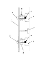
図1は本発明のプリント配線基板を支持するプリント配線基板取り付け台の一例を示す斜視図である。
(Embodiment 1)
Figure 1 is Ru perspective view showing a printed circuit an example of a substrate mounting table for supporting the print wiring board of the present invention.
図2は本発明の図1のサポートピンA上に熱処理されるプリント配線基板1を乗せた斜視図である。 Figure 2 is Ru perspective view der carrying the printed circuit board 1 to be heat-treated on a support pin A 1 of the present invention.
図3は本発明の図2における断面図である。 Figure 3 is Ru sectional view der in Figure 2 of the present invention.
図4は本発明の図3における要部拡大図である。 Figure 4 is Ru enlarged view der in Figure 3 of the present invention.
図1〜図4において、1は熱処理を行うプリント配線基板である。 1 to 4, reference numeral 1 denotes a printed wiring board that performs heat treatment.
6は柱状の空洞底部にマグネット9を配置し、プリント配線基板1を支持、固定を行うサポートピンAであり、台部13とこれよりも小径の筒部14からなる。マグネット9は筒部14の空洞底部に固定配置されており、そのマグネット9の端部から筒部14の空洞開口部までの距離はマグネット9の磁力の影響が実装部品に及ばない程度に保たれている。
7はプリント配線基板を支持するためのサポートピンBである。サポートピンA6,サポートピンB7としては、好ましくは金属または、樹脂により構成される。金属としては、例えばアルミニウム合金、鉄等が使用でき、特にアルミニウム合金は磁化しにくく、耐熱性がある点から好ましい。
8はプリント配線基板1に設けられた基板穴10を貫通させ、サポートピンA6に配置したマグネットとでプリント配線基板1を挟持し、固定するための磁性材料からなる押えピンで、好ましくはステンレススチール材(SS材)により形成される。押えピン8は頭部15と小径のピン部16からなる。また、プリント配線基板1の厚みに応じて押えピン8のピン部16の長さの異なる種類のものを複数用意されている。
8 is through the
9はサポートピンA6の空洞底部に配置され、押えピン8と共にプリント配線基板を挟み込んで固定を行うマグネットであり、例えば、コバルト磁石、フェライト磁石、アルニコ磁石等が用いられる。特に、コバルト磁石は保持力が強く、熱に強いという点から好ましい。プリント配線基板を固定する押えピン8の先端は、図3のように、マグネット9に接触される。
A
10はプリント配線基板1に押えピン8を貫通させるための基板穴である。容易に押えピン8が着脱できるように押えピン8のピン部16の径より大きめの穴であることが好ましい。
11は押えピン8とサポートピンA6の筒部14の空洞内壁との間にできる隙間である。12は押えピン8の頭部とプリント配線基板1との間にできる隙間である。
A
以上のように構成されたにプリント配線基板取り付け台ついて、図1から図4を用いてその動作を説明する。 The operation of the printed wiring board mounting base configured as described above will be described with reference to FIGS.
サポートピンA6,サポートピンB7でプリント配線基板1を支持し、サポートピンA6に内蔵されたマグネット9と押えピン8に発生する磁力によってプリント配線基板1を固定するものである。
The printed wiring board 1 is supported by the support pins A6 and the support pins B7, and the printed wiring board 1 is fixed by the magnetic force generated in the
プリント配線基板を高温の炉内で熱処理を行うと軟化して実装されている部品の重量で図では下方に反るように変形しようとするが、サポートピンB7によっても支持されているので下方の反りは抑制できる。 Suruga to deform so warped downward printed wiring board in FIG weight of components mounted softens with the heat treatment is performed in a high temperature furnace, since by the support pin B7 is supported downwards Can be suppressed.
また、マグネット9をサポートピンA6の筒部14の空洞底部に埋め込んで配置しており、プリント配線基板1とマグネット9の間に一定の距離を設けている。従来技術では半田がペースト状、または炉内で溶融状態のときには実装されるリードにニッケルメッキを施してある電子部品や、ペライト素材のような磁性材料を用いているコイル等の電子部品がマグネット9の磁力によって引き寄せられ、実装位置がずれてしまう不具合が発生していたが、本発明のプリント配線基板取り付け台ではプリント配線基板1とマグネット9の間に一定の距離を設けているのでこのような影響をなくすことができる。
Further, the
また、押えピン8のピン部16の長さの異なる種類のものが複数用意されているのでプリント配線基板1とマグネット9の間の距離は押えピン8のピン部16の長さを変えることで任意に設定できる。
Further, since a plurality of types having different lengths of the
従来技術ではプリント配線基板1下面を載置し支持するのは平板のため、実装部品を配置できなかったが、本発明のプリント配線基板取り付け台ではサポートピンA6,サポートピンB7によりプリント配線基板1を支持するようにしたため、サポートピンA6,サポートピンB7、押さえピン8がプリント配線基板1と当接する位置を除き両面に電子部品が実装されているプリント配線基板にも使用できる。
For to the prior art by placing the printed wiring board 1 the lower surface support is flat, could not be arranged mounted components, printed circuit support pin A6 denotes a substrate mounting base of the present invention, the printed wiring board 1 by the support pin B7 Since the support pins A6, the support pins B7, and the
また、プリント配線基板1に押えピン8を貫通させるための基板穴10を設けることにより、押えピン8を他の電子部品と同様にマウンタでサポートピンA6の空洞に挿入することができる。
Further, by providing the printed wiring board 1 with the
また、押えピン8のピン径はサポートピンA6の筒部14の空洞の径より小さくし、押えピン8のピン部16をサポートピンA6の筒部14の空洞に挿入したときに押えピン8のピン部16とサポートピンAの筒部14の空洞内壁との間に隙間11ができるように構成する。このように、押えピン8とサポートピンA6の筒部14の空洞内壁との間に隙間11を設けることで、面方向のプリント配線基板の膨張を逃がし、プリント配線基板1にストレスを与えないようにしている。この隙間11により反りを防止することができる。
Further, the pin diameter of the
同様の理由によりプリント配線基板1に設けられた基板穴10の穴径に対して押えピン8のピン部径を小さくし、基板穴10と押えピン8との間に隙間を形成する。
For the same reason, the pin portion diameter of the
また、押えピン8とサポートピンA6によりプリント配線基板1を挟持したときに、押えピン8の頭部とサポートピンA6の筒部14の空洞開口部端との間隔をプリント配線基板1の厚みより長くしている。これにより、押えピン8の頭部とプリント配線基板1との間に隙間12を形成することにより、プリント配線基板1の厚み方向の膨張を逃し、プリント配線基板1にストレスを与えないようにしている。この隙間12により反りを防止することができる。
Further, when sandwiching the printed wiring board 1 by the
以上のように本実施の形態によれば、サポートピンA6,サポートピンB7によるプリント配線基板の支持に加え、サポートピンA6に対向して、プリント配線基板1に設けた穴に磁性材料からなる押えピン8を挿入することにより、押えピン8とマグネット9を接触させることにより、強い力でプリント配線基板1を固定することができ、熱処理過程に発生するプリント配線基板1の熱変形を抑制することで、プリント配線基板1に発生する反りを防止することができる。
According to the present embodiment as described above, support pins A6, added by the support pin B7 to the support of the printed circuit board, opposite the support pin A6, consists magnetic material into a hole provided on the printed wiring board 1 by inserting the retainer pins 8, by contacting the
また、マグネット9をサポートピンA6の筒部14の空洞底部に配置することで、プリント配線基板1とマグネット9の間に一定の距離を設けることにより磁性材料を用いた電子部品がマグネット9の磁力によって引き寄せられ、実装位置がずれるというような影響をなくすことができる。
In addition, by disposing the
また、サポートピンA6,サポートピンB7によりプリント配線基板1を支持するために両面の電子部品実装が可能となる。 Further, since the printed wiring board 1 is supported by the support pins A6 and the support pins B7, both-side electronic components can be mounted.
また、隙間11、隙間12を設けることで、プリント配線基板1の面方向、厚み方向の膨張分を各隙間へ逃がし、プリント配線基板1の反りを防止することができる。
Further, by providing the
(実施の形態2)
以下、本発明の実施の形態2について、図5から図10を用いて説明する。
(Embodiment 2)
The second embodiment of the present invention will be described below with reference to FIGS.
図5は本発明のサポートピン上にプリント配線基板を載せた断面図である。 FIG. 5 is a cross-sectional view of a printed wiring board placed on the support pins of the present invention.
図6は本発明のサポートピンA6にサポートピンの長さを変えることができるアタッチメントCを装着させた図である。 FIG. 6 is a view in which an attachment C capable of changing the length of the support pin is attached to the support pin A6 of the present invention.
図5、図6において、1は熱処理を行うプリント配線基板、6はプリント配線基板1の支持、固定を行うマグネットを内蔵したサポートピンAで、7はプリント配線基板を支持するためのサポートピンBである。8はプリント配線基板1を固定するための磁性材料からなる押えピンで、9はプリント配線基板の固定を行うマグネットである。16はサポートピンの長さを変えるアタッチメントCである。
5 and 6, reference numeral 1 denotes a printed wiring board that performs heat treatment, 6 denotes a support pin A that incorporates a magnet that supports and fixes the printed
図7は本発明のサポートピンA6にサポートピンの穴径を小さくするアタッチメントDを装着させた図である。 FIG. 7 is a view in which an attachment D for reducing the hole diameter of the support pin is attached to the support pin A6 of the present invention.
図7において17はサポートピンA6の穴径を小さくできるアタッチメントDであり、好ましくは金属または、樹脂により構成される。金属としては、例えばアルミニウム合金、鉄等が使用でき、特に、アルミニウム合金は入手が容易で、加工し易く軽量で、さらに磁化しにくく、耐熱性がある点から好ましい。
In FIG. 7,
図8は本発明のサポートピンB7に長さを変えることのできるアタッチメントEを装着可能とした図である。 FIG. 8 is a view in which an attachment E whose length can be changed can be attached to the support pin B7 of the present invention.
図8において18はサポートピンB7の長さを変えることのできるアタッチメントEであり、好ましくは金属または、樹脂により構成される。金属としては、例えばアルミニウム合金、鉄等が使用でき、特に、アルミニウム合金は入手が容易で、加工し易く軽量で、さらに磁化しにくく、耐熱性がある点から好ましい。 In FIG. 8, 18 is an attachment E that can change the length of the support pin B7 , and is preferably made of metal or resin. As the metal, for example, an aluminum alloy, iron, or the like can be used. In particular, an aluminum alloy is preferable because it is easily available, easy to process, lightweight, hardly magnetized, and has heat resistance.
図9は本発明の押えピン8にアタッチメントF、F′を装着可能とした図である。
Figure 9 is a diagram in which can be mounted attachments F, F 'the
図9においてアタッチメントF、F′19を押えピン8の先に装着することで、押えピン8の長さを変えたり、先の径を変えることのできるアタッチメントであり、磁性材料からなり、好ましくはSS材により形成される。
In FIG. 9, the attachments F and F′19 are attached to the tip of the
図10は押えピンの他の例を示す図である。 FIG. 10 is a view showing another example of the presser pin.
図10において20は押えピンの頭で、21は押えピンの頭に差し込むことができる押えピンの足部である。押えピンの頭20は非磁性材料からなり、押えピンの足21は磁性材料からなる。
In FIG. 10, 20 is the head of the presser pin, and 21 is the foot of the presser pin that can be inserted into the head of the presser pin. The
図5は図3の構成と同様なものである。図3の構成と異なるのは図6、図7、図8、図9であり、サポートピンA6、サポートピンB7や押えピン8にアタッチメントC16、アタッチメントD17、アタッチメントE18、アタッチメントF、F′19を用意し、押えピンの頭20、押えピンの足部21からなる押えピンを装着することで、サポートピンA6、サポートピンB7や押えピン8の長さや太さの違うものを用意しなくても、アタッチメントを用意するだけで、ピンの長さや太さを変えられるようにしたことを示している。
FIG. 5 is similar to the configuration of FIG. 6, 7, 8, and 9 are different from the configuration of FIG. 3 in that attachment C16, attachment D17, attachment E18, and attachments F and F′19 are attached to the support pin A6, the support pin B7, and the
以上のように構成されたプリント配線基板取り付け台について、以下その動作を説明する。 The operation of the printed wiring board mounting base configured as described above will be described below.
サポートピンA6、サポートピンB7でプリント配線基板1を支持し、サポートピンA6に内蔵されたマグネット9と押えピン8に発生する磁力によってプリント配線基板1を固定するものである。
The printed wiring board 1 is supported by the support pins A6 and the support pins B7, and the printed wiring board 1 is fixed by the magnetic force generated in the
サポートピンA6、サポートピンB7はアタッチメントC16,アタッチメントD17,アタッチメントE18によってその長さや穴径を変更することができるものである。また押えピン8はアタッチメントF、F′19によってその長さや径を変更できるものである。また、押えピン8を頭部20に対して足部21を取り替え可能にすることでその長さや径を変更できるものである。
The support pin A6 and the support pin B7 can be changed in length and hole diameter by an attachment C16, an attachment D17, and an attachment E18. The
以上のように本実施の形態によれば、サポートピンA6、サポートピンB7や押えピン8に対して、アタッチメントC16,アタッチメントD17,アタッチメントE18及び、アタッチメントF、F′19を設けることや、押えピン8の頭部20に対して足部21を取り替え可能にすることにより、サポートピンA6、サポートピンB7や押えピン8の長さや径を変えることができ、複数のピンを用意する必要がなくなり、コスト削減を図ることができる。
As described above, according to the present embodiment, the attachment C16, the attachment D17, the attachment E18, and the attachments F and F′19 are provided for the support pin A6, the support pin B7, and the
なお、以上の説明では押えピンのアタッチメントF、F′19は磁性材料、サポートピンA6に内蔵されるのはマグネット9としたが、アタッチメントF、F′19はマグネットとし、サポートピンA6に内蔵されるものを磁性材料としてもよい。
In the above description, the presser pin attachments F and F'19 are made of magnetic material, and the support pin A6 is built with the
本発明にかかるプリント配線基板取り付け台は、より強い力で熱処理するプリント配線基板を固定できるとともに、プリント配線基板にストレスを与えないでプリント配線基板に発生する反りを抑制し、半田付けされる電子部品に影響を与えないという効果を有し、半田付けするプリント配線基板の反り防止に関したプリント配線基板取り付け台として有用である。 The printed wiring board mounting base according to the present invention can fix the printed wiring board to be heat-treated with a stronger force, suppress the warpage generated in the printed wiring board without applying stress to the printed wiring board, and can be electronically soldered. has the effect of not affecting the components, it is useful as a printed printed circuit board mounting stand wirings related to preventing warpage of the substrate to be soldered.
1 プリント配線基板
6 サポートピンA
7 サポートピンB
8 押えピン
9 マグネット
10 基板穴
13 サポートピンAの台部
14 サポートピンAの筒部
15 押えピンの頭部
16 押えピンのピン部
1 Printed
7 Support pin B
8
Claims (3)
プリント配線基板に設けた基板穴と、
筒部の先端から内部に設けた空洞の底部にマグネットを配置したサポートピンAと、
磁性材料からなり、頭部とその頭部よりも小径のピン部からなる押えピンと、を備え、
前記サポートピンAの筒部の先端に前記プリント配線基板を載置した状態で、そのプリント配線基板の基板穴から前記押えピンのピン部を前記サポートピンAの空洞に挿入し、前記空洞の底部に配置されたマグネットに前記押えピンのピン部を接触させることによりその接触磁力でプリント配線基板をサポートピンAと押えピンにより取り付けることを特徴とするプリント配線基板取り付け台。 A printed wiring board mounting base for supporting the printed circuit board for soldered electronic components in a high temperature furnace,
A board hole provided in the printed wiring board;
A support pin A in which a magnet is arranged at the bottom of a cavity provided inside from the tip of the cylindrical portion;
It is made of a magnetic material, and includes a head and a presser pin made of a pin portion having a smaller diameter than the head,
With the printed wiring board placed on the tip of the cylindrical portion of the support pin A, the pin portion of the holding pin is inserted into the cavity of the support pin A from the board hole of the printed wiring board, and the bottom of the cavity A printed wiring board mounting base characterized in that a printed wiring board is attached by a support pin A and a pressing pin by a contact magnetic force by bringing a pin portion of the pressing pin into contact with a magnet arranged on the magnet.
Priority Applications (1)
| Application Number | Priority Date | Filing Date | Title |
|---|---|---|---|
| JP2007104769A JP4816553B2 (en) | 2007-04-12 | 2007-04-12 | Printed circuit board mounting base |
Applications Claiming Priority (1)
| Application Number | Priority Date | Filing Date | Title |
|---|---|---|---|
| JP2007104769A JP4816553B2 (en) | 2007-04-12 | 2007-04-12 | Printed circuit board mounting base |
Publications (3)
| Publication Number | Publication Date |
|---|---|
| JP2008263065A JP2008263065A (en) | 2008-10-30 |
| JP2008263065A5 JP2008263065A5 (en) | 2010-05-06 |
| JP4816553B2 true JP4816553B2 (en) | 2011-11-16 |
Family
ID=39985320
Family Applications (1)
| Application Number | Title | Priority Date | Filing Date |
|---|---|---|---|
| JP2007104769A Active JP4816553B2 (en) | 2007-04-12 | 2007-04-12 | Printed circuit board mounting base |
Country Status (1)
| Country | Link |
|---|---|
| JP (1) | JP4816553B2 (en) |
Families Citing this family (5)
| Publication number | Priority date | Publication date | Assignee | Title |
|---|---|---|---|---|
| KR101457968B1 (en) * | 2013-06-26 | 2014-11-07 | 미크론정공 주식회사 | Method for manufacturing chase insert of semiconductor die using high temperature surface treatment |
| KR200471840Y1 (en) | 2013-09-09 | 2014-03-17 | (주)보은 | Magnetic structure for heat treatment apparatus of welded zone |
| CN107807318A (en) * | 2016-08-31 | 2018-03-16 | 科大国盾量子技术股份有限公司 | A kind of clamp for testing electronic device |
| CN110303220B (en) * | 2019-08-12 | 2024-04-26 | 无锡华测电子系统有限公司 | Novel double-channel TR assembly reflow soldering tool |
| CN114340151B (en) * | 2022-03-14 | 2022-05-06 | 潍坊学院 | Printed circuit board pad structure |
Family Cites Families (2)
| Publication number | Priority date | Publication date | Assignee | Title |
|---|---|---|---|---|
| JPH04262599A (en) * | 1991-02-18 | 1992-09-17 | Matsushita Electric Ind Co Ltd | Printed board corrector |
| JPH0722794A (en) * | 1993-06-30 | 1995-01-24 | Taiho Seiki Co Ltd | Supporting apparatus for sheetlike member |
-
2007
- 2007-04-12 JP JP2007104769A patent/JP4816553B2/en active Active
Also Published As
| Publication number | Publication date |
|---|---|
| JP2008263065A (en) | 2008-10-30 |
Similar Documents
| Publication | Publication Date | Title |
|---|---|---|
| JP4816553B2 (en) | Printed circuit board mounting base | |
| JP2010098320A (en) | Surface mounting process for flexible printed circuit board, and magnetic tool and steel mesh used in the same | |
| JP2008263065A5 (en) | ||
| CN210202353U (en) | Thin printed circuit board paster frock | |
| JPH1041606A (en) | Relay board, its manufacture, board with relay board, structure constituted of board, relay board and fixing board, its manufacture, and disassemlbing method of the structure | |
| JP5546778B2 (en) | Printed circuit board and printed circuit board manufacturing method | |
| JP2010205992A5 (en) | ||
| JP4545017B2 (en) | Electronic component fixing jig and electronic component processing method | |
| JP2011159664A (en) | Method of manufacturing printed board equipped with through hole connector | |
| JP4985497B2 (en) | Soldering method | |
| JP2006303354A (en) | Printed-wiring board and method for joining the same | |
| JP2009218358A5 (en) | ||
| JP2013025974A (en) | Current auxiliary member | |
| JP2021111753A (en) | Removal method of electronic component | |
| JP3709036B2 (en) | Mounting method for weak heat-resistant electronic components | |
| JP2014110331A (en) | Warpage prevention jig and method of manufacturing circuit board | |
| JP2007180255A (en) | Printed wiring board and substitutive pad | |
| CN218388168U (en) | Wave soldering jig for PCB | |
| JP2012238903A5 (en) | ||
| JP2010003818A (en) | Printed wiring board, mounting structure, and component inserting machine | |
| JP3170086U (en) | Reflow jig structure | |
| JP5397120B2 (en) | Soldering method and soldering apparatus | |
| JP2010258075A (en) | Method of manufacturing electronic component mounting substrate, and method of fixing wiring board | |
| JP2023093056A (en) | Electronic component removing jig | |
| JP2013137281A (en) | Probe device |
Legal Events
| Date | Code | Title | Description |
|---|---|---|---|
| A521 | Written amendment |
Free format text: JAPANESE INTERMEDIATE CODE: A523 Effective date: 20100317 |
|
| A621 | Written request for application examination |
Free format text: JAPANESE INTERMEDIATE CODE: A621 Effective date: 20100317 |
|
| RD01 | Notification of change of attorney |
Free format text: JAPANESE INTERMEDIATE CODE: A7421 Effective date: 20100413 |
|
| A977 | Report on retrieval |
Free format text: JAPANESE INTERMEDIATE CODE: A971007 Effective date: 20110524 |
|
| A131 | Notification of reasons for refusal |
Free format text: JAPANESE INTERMEDIATE CODE: A131 Effective date: 20110531 |
|
| A521 | Written amendment |
Free format text: JAPANESE INTERMEDIATE CODE: A523 Effective date: 20110706 |
|
| TRDD | Decision of grant or rejection written | ||
| A01 | Written decision to grant a patent or to grant a registration (utility model) |
Free format text: JAPANESE INTERMEDIATE CODE: A01 Effective date: 20110802 |
|
| A01 | Written decision to grant a patent or to grant a registration (utility model) |
Free format text: JAPANESE INTERMEDIATE CODE: A01 |
|
| A61 | First payment of annual fees (during grant procedure) |
Free format text: JAPANESE INTERMEDIATE CODE: A61 Effective date: 20110815 |
|
| FPAY | Renewal fee payment (event date is renewal date of database) |
Free format text: PAYMENT UNTIL: 20140909 Year of fee payment: 3 |
|
| R151 | Written notification of patent or utility model registration |
Ref document number: 4816553 Country of ref document: JP Free format text: JAPANESE INTERMEDIATE CODE: R151 |
|
| FPAY | Renewal fee payment (event date is renewal date of database) |
Free format text: PAYMENT UNTIL: 20140909 Year of fee payment: 3 |