JP4805141B2 - Electroplating equipment - Google Patents
Electroplating equipment Download PDFInfo
- Publication number
- JP4805141B2 JP4805141B2 JP2006507663A JP2006507663A JP4805141B2 JP 4805141 B2 JP4805141 B2 JP 4805141B2 JP 2006507663 A JP2006507663 A JP 2006507663A JP 2006507663 A JP2006507663 A JP 2006507663A JP 4805141 B2 JP4805141 B2 JP 4805141B2
- Authority
- JP
- Japan
- Prior art keywords
- plating
- plated
- substrate
- plating solution
- tank
- Prior art date
- Legal status (The legal status is an assumption and is not a legal conclusion. Google has not performed a legal analysis and makes no representation as to the accuracy of the status listed.)
- Expired - Fee Related
Links
- 238000009713 electroplating Methods 0.000 title claims description 49
- 238000007747 plating Methods 0.000 claims description 495
- 239000000243 solution Substances 0.000 claims description 215
- 238000003756 stirring Methods 0.000 claims description 149
- 239000000463 material Substances 0.000 claims description 72
- 239000007921 spray Substances 0.000 claims description 19
- 238000002347 injection Methods 0.000 claims description 18
- 239000007924 injection Substances 0.000 claims description 18
- 238000005192 partition Methods 0.000 claims description 10
- 239000012777 electrically insulating material Substances 0.000 claims description 4
- 239000000758 substrate Substances 0.000 description 251
- 230000007246 mechanism Effects 0.000 description 51
- 238000000034 method Methods 0.000 description 32
- XLYOFNOQVPJJNP-UHFFFAOYSA-N water Substances O XLYOFNOQVPJJNP-UHFFFAOYSA-N 0.000 description 25
- 238000012546 transfer Methods 0.000 description 17
- 238000009826 distribution Methods 0.000 description 15
- 239000002184 metal Substances 0.000 description 15
- 229910052751 metal Inorganic materials 0.000 description 15
- 230000033001 locomotion Effects 0.000 description 14
- 230000008569 process Effects 0.000 description 14
- 238000005406 washing Methods 0.000 description 14
- 238000012545 processing Methods 0.000 description 13
- 238000007772 electroless plating Methods 0.000 description 11
- 230000004913 activation Effects 0.000 description 10
- 239000004065 semiconductor Substances 0.000 description 9
- 238000004140 cleaning Methods 0.000 description 8
- 230000032258 transport Effects 0.000 description 8
- 238000001035 drying Methods 0.000 description 7
- 239000007788 liquid Substances 0.000 description 6
- VEXZGXHMUGYJMC-UHFFFAOYSA-N Hydrochloric acid Chemical compound Cl VEXZGXHMUGYJMC-UHFFFAOYSA-N 0.000 description 4
- 238000013019 agitation Methods 0.000 description 4
- 238000004090 dissolution Methods 0.000 description 4
- 230000002093 peripheral effect Effects 0.000 description 4
- 239000000126 substance Substances 0.000 description 4
- QAOWNCQODCNURD-UHFFFAOYSA-N sulfuric acid group Chemical group S(O)(O)(=O)=O QAOWNCQODCNURD-UHFFFAOYSA-N 0.000 description 4
- 230000008901 benefit Effects 0.000 description 3
- 230000015572 biosynthetic process Effects 0.000 description 3
- 230000008859 change Effects 0.000 description 3
- 150000002500 ions Chemical class 0.000 description 3
- 230000004048 modification Effects 0.000 description 3
- 238000012986 modification Methods 0.000 description 3
- 239000011347 resin Substances 0.000 description 3
- 229920005989 resin Polymers 0.000 description 3
- 238000005507 spraying Methods 0.000 description 3
- CSCPPACGZOOCGX-UHFFFAOYSA-N Acetone Chemical compound CC(C)=O CSCPPACGZOOCGX-UHFFFAOYSA-N 0.000 description 2
- PXHVJJICTQNCMI-UHFFFAOYSA-N Nickel Chemical compound [Ni] PXHVJJICTQNCMI-UHFFFAOYSA-N 0.000 description 2
- 239000004696 Poly ether ether ketone Substances 0.000 description 2
- JUPQTSLXMOCDHR-UHFFFAOYSA-N benzene-1,4-diol;bis(4-fluorophenyl)methanone Chemical compound OC1=CC=C(O)C=C1.C1=CC(F)=CC=C1C(=O)C1=CC=C(F)C=C1 JUPQTSLXMOCDHR-UHFFFAOYSA-N 0.000 description 2
- 230000007547 defect Effects 0.000 description 2
- 230000002542 deteriorative effect Effects 0.000 description 2
- 238000010586 diagram Methods 0.000 description 2
- 230000005684 electric field Effects 0.000 description 2
- 239000011261 inert gas Substances 0.000 description 2
- 230000002452 interceptive effect Effects 0.000 description 2
- WABPQHHGFIMREM-UHFFFAOYSA-N lead(0) Chemical compound [Pb] WABPQHHGFIMREM-UHFFFAOYSA-N 0.000 description 2
- 229910021645 metal ion Inorganic materials 0.000 description 2
- 229920002530 polyetherether ketone Polymers 0.000 description 2
- 239000004810 polytetrafluoroethylene Substances 0.000 description 2
- 229920001343 polytetrafluoroethylene Polymers 0.000 description 2
- 238000007781 pre-processing Methods 0.000 description 2
- 238000002203 pretreatment Methods 0.000 description 2
- 229910000679 solder Inorganic materials 0.000 description 2
- RYGMFSIKBFXOCR-UHFFFAOYSA-N Copper Chemical compound [Cu] RYGMFSIKBFXOCR-UHFFFAOYSA-N 0.000 description 1
- XUIMIQQOPSSXEZ-UHFFFAOYSA-N Silicon Chemical compound [Si] XUIMIQQOPSSXEZ-UHFFFAOYSA-N 0.000 description 1
- 238000007664 blowing Methods 0.000 description 1
- 230000003749 cleanliness Effects 0.000 description 1
- 229910052802 copper Inorganic materials 0.000 description 1
- 239000010949 copper Substances 0.000 description 1
- 230000000593 degrading effect Effects 0.000 description 1
- 238000007599 discharging Methods 0.000 description 1
- 230000000694 effects Effects 0.000 description 1
- 238000005516 engineering process Methods 0.000 description 1
- 238000005530 etching Methods 0.000 description 1
- PCHJSUWPFVWCPO-UHFFFAOYSA-N gold Chemical compound [Au] PCHJSUWPFVWCPO-UHFFFAOYSA-N 0.000 description 1
- 229910052737 gold Inorganic materials 0.000 description 1
- 239000010931 gold Substances 0.000 description 1
- 238000012423 maintenance Methods 0.000 description 1
- 238000007726 management method Methods 0.000 description 1
- 238000004519 manufacturing process Methods 0.000 description 1
- 229910052759 nickel Inorganic materials 0.000 description 1
- 238000002161 passivation Methods 0.000 description 1
- 238000007639 printing Methods 0.000 description 1
- 229910052710 silicon Inorganic materials 0.000 description 1
- 239000010703 silicon Substances 0.000 description 1
- 239000002904 solvent Substances 0.000 description 1
- 230000007480 spreading Effects 0.000 description 1
- 238000003892 spreading Methods 0.000 description 1
- 238000007740 vapor deposition Methods 0.000 description 1
Images


Classifications
-
- C—CHEMISTRY; METALLURGY
- C25—ELECTROLYTIC OR ELECTROPHORETIC PROCESSES; APPARATUS THEREFOR
- C25D—PROCESSES FOR THE ELECTROLYTIC OR ELECTROPHORETIC PRODUCTION OF COATINGS; ELECTROFORMING; APPARATUS THEREFOR
- C25D17/00—Constructional parts, or assemblies thereof, of cells for electrolytic coating
- C25D17/008—Current shielding devices
-
- C—CHEMISTRY; METALLURGY
- C23—COATING METALLIC MATERIAL; COATING MATERIAL WITH METALLIC MATERIAL; CHEMICAL SURFACE TREATMENT; DIFFUSION TREATMENT OF METALLIC MATERIAL; COATING BY VACUUM EVAPORATION, BY SPUTTERING, BY ION IMPLANTATION OR BY CHEMICAL VAPOUR DEPOSITION, IN GENERAL; INHIBITING CORROSION OF METALLIC MATERIAL OR INCRUSTATION IN GENERAL
- C23C—COATING METALLIC MATERIAL; COATING MATERIAL WITH METALLIC MATERIAL; SURFACE TREATMENT OF METALLIC MATERIAL BY DIFFUSION INTO THE SURFACE, BY CHEMICAL CONVERSION OR SUBSTITUTION; COATING BY VACUUM EVAPORATION, BY SPUTTERING, BY ION IMPLANTATION OR BY CHEMICAL VAPOUR DEPOSITION, IN GENERAL
- C23C18/00—Chemical coating by decomposition of either liquid compounds or solutions of the coating forming compounds, without leaving reaction products of surface material in the coating; Contact plating
- C23C18/16—Chemical coating by decomposition of either liquid compounds or solutions of the coating forming compounds, without leaving reaction products of surface material in the coating; Contact plating by reduction or substitution, e.g. electroless plating
- C23C18/1601—Process or apparatus
- C23C18/1619—Apparatus for electroless plating
- C23C18/1628—Specific elements or parts of the apparatus
-
- C—CHEMISTRY; METALLURGY
- C25—ELECTROLYTIC OR ELECTROPHORETIC PROCESSES; APPARATUS THEREFOR
- C25D—PROCESSES FOR THE ELECTROLYTIC OR ELECTROPHORETIC PRODUCTION OF COATINGS; ELECTROFORMING; APPARATUS THEREFOR
- C25D17/00—Constructional parts, or assemblies thereof, of cells for electrolytic coating
- C25D17/001—Apparatus specially adapted for electrolytic coating of wafers, e.g. semiconductors or solar cells
-
- C—CHEMISTRY; METALLURGY
- C25—ELECTROLYTIC OR ELECTROPHORETIC PROCESSES; APPARATUS THEREFOR
- C25D—PROCESSES FOR THE ELECTROLYTIC OR ELECTROPHORETIC PRODUCTION OF COATINGS; ELECTROFORMING; APPARATUS THEREFOR
- C25D21/00—Processes for servicing or operating cells for electrolytic coating
- C25D21/10—Agitating of electrolytes; Moving of racks
-
- C—CHEMISTRY; METALLURGY
- C25—ELECTROLYTIC OR ELECTROPHORETIC PROCESSES; APPARATUS THEREFOR
- C25D—PROCESSES FOR THE ELECTROLYTIC OR ELECTROPHORETIC PRODUCTION OF COATINGS; ELECTROFORMING; APPARATUS THEREFOR
- C25D5/00—Electroplating characterised by the process; Pretreatment or after-treatment of workpieces
- C25D5/08—Electroplating with moving electrolyte e.g. jet electroplating
-
- C—CHEMISTRY; METALLURGY
- C25—ELECTROLYTIC OR ELECTROPHORETIC PROCESSES; APPARATUS THEREFOR
- C25D—PROCESSES FOR THE ELECTROLYTIC OR ELECTROPHORETIC PRODUCTION OF COATINGS; ELECTROFORMING; APPARATUS THEREFOR
- C25D7/00—Electroplating characterised by the article coated
- C25D7/12—Semiconductors
- C25D7/123—Semiconductors first coated with a seed layer or a conductive layer
-
- H—ELECTRICITY
- H01—ELECTRIC ELEMENTS
- H01L—SEMICONDUCTOR DEVICES NOT COVERED BY CLASS H10
- H01L24/00—Arrangements for connecting or disconnecting semiconductor or solid-state bodies; Methods or apparatus related thereto
- H01L24/01—Means for bonding being attached to, or being formed on, the surface to be connected, e.g. chip-to-package, die-attach, "first-level" interconnects; Manufacturing methods related thereto
- H01L24/10—Bump connectors ; Manufacturing methods related thereto
- H01L24/11—Manufacturing methods
-
- H—ELECTRICITY
- H01—ELECTRIC ELEMENTS
- H01L—SEMICONDUCTOR DEVICES NOT COVERED BY CLASS H10
- H01L21/00—Processes or apparatus adapted for the manufacture or treatment of semiconductor or solid state devices or of parts thereof
- H01L21/02—Manufacture or treatment of semiconductor devices or of parts thereof
- H01L21/04—Manufacture or treatment of semiconductor devices or of parts thereof the devices having potential barriers, e.g. a PN junction, depletion layer or carrier concentration layer
- H01L21/18—Manufacture or treatment of semiconductor devices or of parts thereof the devices having potential barriers, e.g. a PN junction, depletion layer or carrier concentration layer the devices having semiconductor bodies comprising elements of Group IV of the Periodic Table or AIIIBV compounds with or without impurities, e.g. doping materials
- H01L21/28—Manufacture of electrodes on semiconductor bodies using processes or apparatus not provided for in groups H01L21/20 - H01L21/268
- H01L21/283—Deposition of conductive or insulating materials for electrodes conducting electric current
- H01L21/288—Deposition of conductive or insulating materials for electrodes conducting electric current from a liquid, e.g. electrolytic deposition
- H01L21/2885—Deposition of conductive or insulating materials for electrodes conducting electric current from a liquid, e.g. electrolytic deposition using an external electrical current, i.e. electro-deposition
-
- H—ELECTRICITY
- H01—ELECTRIC ELEMENTS
- H01L—SEMICONDUCTOR DEVICES NOT COVERED BY CLASS H10
- H01L2224/00—Indexing scheme for arrangements for connecting or disconnecting semiconductor or solid-state bodies and methods related thereto as covered by H01L24/00
- H01L2224/01—Means for bonding being attached to, or being formed on, the surface to be connected, e.g. chip-to-package, die-attach, "first-level" interconnects; Manufacturing methods related thereto
- H01L2224/02—Bonding areas; Manufacturing methods related thereto
- H01L2224/04—Structure, shape, material or disposition of the bonding areas prior to the connecting process
- H01L2224/05—Structure, shape, material or disposition of the bonding areas prior to the connecting process of an individual bonding area
- H01L2224/0554—External layer
- H01L2224/0556—Disposition
- H01L2224/05568—Disposition the whole external layer protruding from the surface
-
- H—ELECTRICITY
- H01—ELECTRIC ELEMENTS
- H01L—SEMICONDUCTOR DEVICES NOT COVERED BY CLASS H10
- H01L2224/00—Indexing scheme for arrangements for connecting or disconnecting semiconductor or solid-state bodies and methods related thereto as covered by H01L24/00
- H01L2224/01—Means for bonding being attached to, or being formed on, the surface to be connected, e.g. chip-to-package, die-attach, "first-level" interconnects; Manufacturing methods related thereto
- H01L2224/02—Bonding areas; Manufacturing methods related thereto
- H01L2224/04—Structure, shape, material or disposition of the bonding areas prior to the connecting process
- H01L2224/05—Structure, shape, material or disposition of the bonding areas prior to the connecting process of an individual bonding area
- H01L2224/0554—External layer
- H01L2224/05573—Single external layer
-
- H—ELECTRICITY
- H01—ELECTRIC ELEMENTS
- H01L—SEMICONDUCTOR DEVICES NOT COVERED BY CLASS H10
- H01L2224/00—Indexing scheme for arrangements for connecting or disconnecting semiconductor or solid-state bodies and methods related thereto as covered by H01L24/00
- H01L2224/01—Means for bonding being attached to, or being formed on, the surface to be connected, e.g. chip-to-package, die-attach, "first-level" interconnects; Manufacturing methods related thereto
- H01L2224/10—Bump connectors; Manufacturing methods related thereto
- H01L2224/11—Manufacturing methods
- H01L2224/1147—Manufacturing methods using a lift-off mask
-
- H—ELECTRICITY
- H01—ELECTRIC ELEMENTS
- H01L—SEMICONDUCTOR DEVICES NOT COVERED BY CLASS H10
- H01L2224/00—Indexing scheme for arrangements for connecting or disconnecting semiconductor or solid-state bodies and methods related thereto as covered by H01L24/00
- H01L2224/01—Means for bonding being attached to, or being formed on, the surface to be connected, e.g. chip-to-package, die-attach, "first-level" interconnects; Manufacturing methods related thereto
- H01L2224/10—Bump connectors; Manufacturing methods related thereto
- H01L2224/12—Structure, shape, material or disposition of the bump connectors prior to the connecting process
- H01L2224/13—Structure, shape, material or disposition of the bump connectors prior to the connecting process of an individual bump connector
- H01L2224/13001—Core members of the bump connector
- H01L2224/13099—Material
-
- H—ELECTRICITY
- H01—ELECTRIC ELEMENTS
- H01L—SEMICONDUCTOR DEVICES NOT COVERED BY CLASS H10
- H01L2924/00—Indexing scheme for arrangements or methods for connecting or disconnecting semiconductor or solid-state bodies as covered by H01L24/00
- H01L2924/01—Chemical elements
- H01L2924/01004—Beryllium [Be]
-
- H—ELECTRICITY
- H01—ELECTRIC ELEMENTS
- H01L—SEMICONDUCTOR DEVICES NOT COVERED BY CLASS H10
- H01L2924/00—Indexing scheme for arrangements or methods for connecting or disconnecting semiconductor or solid-state bodies as covered by H01L24/00
- H01L2924/01—Chemical elements
- H01L2924/01005—Boron [B]
-
- H—ELECTRICITY
- H01—ELECTRIC ELEMENTS
- H01L—SEMICONDUCTOR DEVICES NOT COVERED BY CLASS H10
- H01L2924/00—Indexing scheme for arrangements or methods for connecting or disconnecting semiconductor or solid-state bodies as covered by H01L24/00
- H01L2924/01—Chemical elements
- H01L2924/01006—Carbon [C]
-
- H—ELECTRICITY
- H01—ELECTRIC ELEMENTS
- H01L—SEMICONDUCTOR DEVICES NOT COVERED BY CLASS H10
- H01L2924/00—Indexing scheme for arrangements or methods for connecting or disconnecting semiconductor or solid-state bodies as covered by H01L24/00
- H01L2924/01—Chemical elements
- H01L2924/01015—Phosphorus [P]
-
- H—ELECTRICITY
- H01—ELECTRIC ELEMENTS
- H01L—SEMICONDUCTOR DEVICES NOT COVERED BY CLASS H10
- H01L2924/00—Indexing scheme for arrangements or methods for connecting or disconnecting semiconductor or solid-state bodies as covered by H01L24/00
- H01L2924/01—Chemical elements
- H01L2924/01023—Vanadium [V]
-
- H—ELECTRICITY
- H01—ELECTRIC ELEMENTS
- H01L—SEMICONDUCTOR DEVICES NOT COVERED BY CLASS H10
- H01L2924/00—Indexing scheme for arrangements or methods for connecting or disconnecting semiconductor or solid-state bodies as covered by H01L24/00
- H01L2924/01—Chemical elements
- H01L2924/01029—Copper [Cu]
-
- H—ELECTRICITY
- H01—ELECTRIC ELEMENTS
- H01L—SEMICONDUCTOR DEVICES NOT COVERED BY CLASS H10
- H01L2924/00—Indexing scheme for arrangements or methods for connecting or disconnecting semiconductor or solid-state bodies as covered by H01L24/00
- H01L2924/01—Chemical elements
- H01L2924/01033—Arsenic [As]
-
- H—ELECTRICITY
- H01—ELECTRIC ELEMENTS
- H01L—SEMICONDUCTOR DEVICES NOT COVERED BY CLASS H10
- H01L2924/00—Indexing scheme for arrangements or methods for connecting or disconnecting semiconductor or solid-state bodies as covered by H01L24/00
- H01L2924/01—Chemical elements
- H01L2924/01074—Tungsten [W]
-
- H—ELECTRICITY
- H01—ELECTRIC ELEMENTS
- H01L—SEMICONDUCTOR DEVICES NOT COVERED BY CLASS H10
- H01L2924/00—Indexing scheme for arrangements or methods for connecting or disconnecting semiconductor or solid-state bodies as covered by H01L24/00
- H01L2924/01—Chemical elements
- H01L2924/01076—Osmium [Os]
-
- H—ELECTRICITY
- H01—ELECTRIC ELEMENTS
- H01L—SEMICONDUCTOR DEVICES NOT COVERED BY CLASS H10
- H01L2924/00—Indexing scheme for arrangements or methods for connecting or disconnecting semiconductor or solid-state bodies as covered by H01L24/00
- H01L2924/01—Chemical elements
- H01L2924/01078—Platinum [Pt]
-
- H—ELECTRICITY
- H01—ELECTRIC ELEMENTS
- H01L—SEMICONDUCTOR DEVICES NOT COVERED BY CLASS H10
- H01L2924/00—Indexing scheme for arrangements or methods for connecting or disconnecting semiconductor or solid-state bodies as covered by H01L24/00
- H01L2924/01—Chemical elements
- H01L2924/01079—Gold [Au]
-
- H—ELECTRICITY
- H01—ELECTRIC ELEMENTS
- H01L—SEMICONDUCTOR DEVICES NOT COVERED BY CLASS H10
- H01L2924/00—Indexing scheme for arrangements or methods for connecting or disconnecting semiconductor or solid-state bodies as covered by H01L24/00
- H01L2924/01—Chemical elements
- H01L2924/01082—Lead [Pb]
-
- H—ELECTRICITY
- H01—ELECTRIC ELEMENTS
- H01L—SEMICONDUCTOR DEVICES NOT COVERED BY CLASS H10
- H01L2924/00—Indexing scheme for arrangements or methods for connecting or disconnecting semiconductor or solid-state bodies as covered by H01L24/00
- H01L2924/013—Alloys
- H01L2924/014—Solder alloys
-
- H—ELECTRICITY
- H01—ELECTRIC ELEMENTS
- H01L—SEMICONDUCTOR DEVICES NOT COVERED BY CLASS H10
- H01L2924/00—Indexing scheme for arrangements or methods for connecting or disconnecting semiconductor or solid-state bodies as covered by H01L24/00
- H01L2924/10—Details of semiconductor or other solid state devices to be connected
- H01L2924/11—Device type
- H01L2924/14—Integrated circuits
Landscapes
- Chemical & Material Sciences (AREA)
- Engineering & Computer Science (AREA)
- Chemical Kinetics & Catalysis (AREA)
- Materials Engineering (AREA)
- Metallurgy (AREA)
- Organic Chemistry (AREA)
- Electrochemistry (AREA)
- Mechanical Engineering (AREA)
- General Chemical & Material Sciences (AREA)
- Life Sciences & Earth Sciences (AREA)
- Sustainable Development (AREA)
- Manufacturing & Machinery (AREA)
- Computer Hardware Design (AREA)
- Microelectronics & Electronic Packaging (AREA)
- Power Engineering (AREA)
- Electroplating Methods And Accessories (AREA)
- Chemically Coating (AREA)
- Internal Circuitry In Semiconductor Integrated Circuit Devices (AREA)
Description
本発明は、基板等の表面(被めっき面)にめっきを施す電気めっき装置に係り、特にめっき技術を用いてLSI用の基板に金属膜付けや配線を形成したり、半導体ウェーハ等の表面に設けられた微細な配線用溝(トレンチ)やビヤホール、レジスト開口部にめっき膜を形成したり、半導体ウェーハの表面にパッケージの電極等と電気的に接続するバンプ(突起状電極)を形成したりするのに使用される電気めっき装置に関する。 The present invention relates to an electroplating apparatus for performing a plating on the surface (surface to be plated) of the substrate or the like, or a metal film is formed with or wiring board for LSI, especially using a plating technique, the surface of a semiconductor wafer Plating film is formed in the fine wiring trench (trench), via hole, and resist opening provided, and bumps (projection electrodes) are formed on the surface of the semiconductor wafer to be electrically connected to package electrodes, etc. It relates electroplating apparatus used to.
近年、半導体回路の配線やバンプを形成する方法として、めっき技術を用いてシリコンウエハまたは他の基板上に金属膜を形成する方法が採用されるようになってきている。 In recent years, a method of forming a metal film on a silicon wafer or another substrate using a plating technique has been adopted as a method of forming wiring and bumps of a semiconductor circuit.
例えば、TAB(Tape Automated Bonding)やFC(フリップチップ)においては、配線が形成された半導体チップの表面の所定箇所(電極)に金、銅、はんだ、或いは鉛フリーはんだやニッケル、更にはこれらを多層に積層した突起状接続電極(バンプ)を形成し、このバンプを介して配線をパッケージの電極やTAB電極に電気的に接続することが広く行われている。このバンプの形成方法としては、めっき法、蒸着法、印刷法、ボールバンプ法といった種々の手法がある。半導体チップのI/O数の増加、細ピッチ化に伴い、微細化が可能で性能が比較的安定しているめっき法が多く用いられるようになってきている。 For example, in TAB (Tape Automated Bonding) and FC (flip chip), gold, copper, solder, lead-free solder, nickel, and these are applied to a predetermined portion (electrode) on the surface of a semiconductor chip on which wiring is formed. It is widely practiced to form projecting connection electrodes (bumps) stacked in multiple layers and to electrically connect the wiring to the package electrode or TAB electrode via the bumps. As a method of forming the bump, there are various methods such as a plating method, a vapor deposition method, a printing method, and a ball bump method. As the number of I / Os of semiconductor chips increases and the pitch becomes finer, plating methods that can be miniaturized and have relatively stable performance are increasingly used.
特に、電気めっきによって得られる金属膜は、高純度で、膜形成速度が速く、膜厚制御方法が簡単であるという利点がある。一方、無電解めっきは、基板等の被めっき材上に通電のためのシード膜が不要であるため、配線やバンプ形成のための工程数が少なくてすむという利点がある。半導体基板上への膜形成においては、膜厚の均一性が厳しく要求されるため、双方のめっき方法においても、従来から多くの検討がなされてきた。 In particular, a metal film obtained by electroplating has advantages of high purity, a high film formation speed, and a simple film thickness control method. On the other hand, electroless plating does not require a seed film for energization on a material to be plated such as a substrate, and therefore has an advantage that the number of steps for wiring and bump formation can be reduced. In film formation on a semiconductor substrate, since uniformity of film thickness is strictly required, many studies have been made on both plating methods.
図27は、いわゆるフェースダウン方式を採用した従来の無電解めっき装置の一例を示す。この無電解めっき装置は、内部にめっき液(無電解めっき液)10を保持する上方に開口しためっき槽12と、被めっき材としての基板Wをその表面(被めっき面)を下向き(フェースダウン)にして着脱自在に保持する上下動自在な基板ホルダ14を有している。めっき槽12の上部の周囲には、オーバフロー槽16が設けられ、このオーバフロー槽16には、めっき液排出ライン18が連結されている。また、めっき槽12の底部には、めっき液供給ライン20に接続されためっき液供給ノズル22が備えられている。
FIG. 27 shows an example of a conventional electroless plating apparatus employing a so-called face-down method. This electroless plating apparatus has a plating
操作に際し、基板ホルダ14で水平に保持した基板Wを、めっき槽12の上端開口部を塞ぐ位置に配置する。この状態で、めっき液供給ノズル22からめっき槽12の内部にめっき液10を供給し、このめっき液10をめっき槽12の上部からオーバフローさせることで、めっき液10を基板ホルダ14で保持した基板Wの表面に沿って流し、めっき液排出ライン18を経て、循環槽(図示せず)に戻す。これにより、前処理を施された基板Wの表面にめっき液10が触れることにより金属が析出して金属膜が形成される。
In operation, the substrate W held horizontally by the
このめっき装置によれば、めっき液供給ノズル22からの供給されるめっき液10の供給速度等を調整したり、基板ホルダ14を回転したりすることにより、基板Wの表面に形成される金属膜の膜厚の均一性をある程度調節することができる。
According to this plating apparatus, the metal film formed on the surface of the substrate W by adjusting the supply rate of the
図28は、いわゆるディップ方式を採用した従来の電気めっき装置の一例を示す。この電気めっき装置は、内部にめっき液(電気めっき液)を保持するめっき槽12aと、基板Wをその周縁部を水密的にシールし表面(被めっき面)を露出させて着脱自在に保持する上下動自在な基板ホルダ14aを有している。めっき槽12aの内部には、アノード24がアノードホルダ26に保持されて垂直に配置されている。更に、基板ホルダ14aで保持した基板Wがアノード24と対向する位置に配置された時に、このアノード24と基板Wとの間に位置するように、中央孔28aを有する誘電体からなる調整板(レギュレーションプレート)28がめっき槽12a内に配置されている。
FIG. 28 shows an example of a conventional electroplating apparatus employing a so-called dip method. In this electroplating apparatus, a
操作に際し、アノード24、基板W及び調整板28をめっき槽12a内のめっき液中に浸漬させる。同時に、導線30aを介してアノード24をめっき電源32の陽極に、導線30bを介して基板Wをめっき電源32の陰極にそれぞれ接続する。これにより、基板Wとアノード24との電位差で、めっき液中の金属イオンが基板Wの表面より電子を受け取り、基板Wの表面に金属が析出して金属膜が形成される。
In operation, the
このめっき装置によれば、アノード24と該アノード24と対向する位置に配置される基板Wとの間に、中央孔28aを有する調整板28を配置し、この調整板28でめっき槽12a内の電位分布を調節することで、基板Wの表面に形成される金属膜の膜厚分布をある程度調節することができる。
According to this plating apparatus, the adjusting
図29は、いわゆるディップ方式を採用した従来の電気めっき装置の他の例を示す。この電気めっき装置の図28に示す電気めっき装置と異なる点は、調整板の代わりにリング状の擬似陰極(擬似電極)34を備え、基板Wの周囲に擬似陰極34を配置した状態で、基板Wを基板ホルダ14aで保持し、更に、めっき処理の際に、導線30cを介して、擬似陰極34をめっき電源32の陰極に接続するようにした点にある。
このめっき装置によれば、擬似陰極34の電位を調節することで、基板Wの表面に形成される金属膜の膜厚の均一性を改善することができる。
FIG. 29 shows another example of a conventional electroplating apparatus employing a so-called dip method. This electroplating apparatus differs from the electroplating apparatus shown in FIG. 28 in that a substrate is provided with a ring-like pseudo cathode (pseudo electrode) 34 instead of the adjustment plate, and the
According to this plating apparatus, the uniformity of the film thickness of the metal film formed on the surface of the substrate W can be improved by adjusting the potential of the
図30は、いわゆるディップ方式を採用した従来の電気めっき装置の更に他の例を示す。この電気めっき装置の図28に示す電気めっき装置と異なる点は、調整板を備えることなく、めっき槽12aの上方に位置して、基板ホルダ14aとアノード24との間にパドルシャフト(攪拌機構)36を平行に配置し、このパドルシャフト36の下面に複数の攪拌翼としてのパドル(掻き混ぜ棒)38をほぼ垂直に垂設して、めっき処理中に、パドルシャフト36を介してパドル38を基板Wと平行に往復動させてめっき槽12a内のめっき液を攪拌するようにした点にある。
FIG. 30 shows still another example of a conventional electroplating apparatus employing a so-called dip method. This electroplating apparatus is different from the electroplating apparatus shown in FIG. 28 in that a paddle shaft (stirring mechanism) is provided between the
このめっき装置によれば、パドルシャフト36を介してパドル38を基板Wと平行に往復動させることで、基板Wの表面に沿っためっき液の流れを、基板Wの表面の全面でより均等にして(めっき液の流れの方向性をなくして)、基板Wの全面に亘ってより均一な膜厚のめっき膜を形成することができる。
According to this plating apparatus, the flow of the plating solution along the surface of the substrate W is made more uniform over the entire surface of the substrate W by reciprocating the
例えば、半導体基板(ウェーハ)の表面に配線用やバンプなどの金属膜(めっき膜)を形成する際、基板の全面に亘って形成した金属膜の表面形状および膜厚の均一性が要求される。近年のSOC、WL−CSPなどの高密度実装技術においては、高精度の均一性が益々を要求されるようになってきたが、従来のめっき装置では、高精度の均一性に応えた金属膜を形成することは非常に困難であった。 For example, when forming a metal film (plating film) for wiring or bumps on the surface of a semiconductor substrate (wafer), the surface shape and film thickness uniformity of the metal film formed over the entire surface of the substrate are required. . In high-density mounting technologies such as SOC and WL-CSP in recent years, high precision uniformity has been increasingly required, but in conventional plating apparatuses, metal films that respond to high precision uniformity. It was very difficult to form.
つまり、従来の各めっき装置は、それぞれの構成特徴によりそれぞれのめっき膜の膜厚分布特性を示すが、これらを改善し、より良好な膜厚均一性を有するめっき膜を得ることが要求されている。均一な膜厚のめっき膜を得るためには、基板表面等の被めっき面近傍におけるめっき液の流れを均一にすることが有効な手段の一つである。めっき液の均一な流れを作り、基板表面等の被めっき面にめっき液を接触させる手法が要求されている。めっき装置自体が簡単な構造で、メンテナンスしやすい構造や機構も求められている。例えば、図29に示すめっき装置では、擬似電極の調整や擬似電極についためっき金属の除去という操作が必要になってくる。このように、操作や管理上の煩雑性問題が生じない、より取り扱いやすくて管理方法の簡便さがめっき装置に求められる。また、めっき時間を短縮するために、めっき速度を上げることが強く望まれている。めっき速度を上げるために、基板等の被めっき面にめっき液中の金属イオンを効率良く供給することが必要となる。 In other words, each conventional plating apparatus shows the film thickness distribution characteristics of each plating film depending on the respective structural characteristics, but it is required to improve these and obtain a plating film having better film thickness uniformity. Yes. In order to obtain a plating film having a uniform film thickness, it is one of effective means to make the flow of the plating solution near the surface to be plated such as the substrate surface. There is a demand for a method for making a uniform flow of a plating solution and bringing the plating solution into contact with a surface to be plated such as a substrate surface. There is also a demand for a structure and mechanism that allows the plating apparatus itself to have a simple structure and easy maintenance. For example, in the plating apparatus shown in FIG. 29 , operations for adjusting the pseudo electrode and removing the plating metal attached to the pseudo electrode are required. As described above, the plating apparatus is required to be easy to handle and easy to manage without causing any trouble in operation and management. Further, it is strongly desired to increase the plating rate in order to shorten the plating time. In order to increase the plating speed, it is necessary to efficiently supply metal ions in the plating solution to the surface to be plated such as a substrate.
電気めっきにあっては、電流密度を上げることでめっき速度を上げることができる。しかし、単に電流密度を上げると、めっきやけ、めっき欠陥、アノード表面の不動態化等が生じて、めっき不具合の原因となってしまう。 In electroplating, the plating rate can be increased by increasing the current density. However, simply increasing the current density causes plating burns, plating defects, passivation of the anode surface, and the like, causing plating defects.
本発明は上記事情に鑑みて為されたもので、比較的簡単な構成で、めっき速度を高め、しかもめっき槽内のめっき液の流れをより均一に調節して、めっき膜の膜厚の面内均一性をより高めることができるようにした電気めっき装置を提供することを目的とする。 The present invention has been made in view of the above circumstances, has a relatively simple configuration, increases the plating speed, and more uniformly adjusts the flow of the plating solution in the plating tank, thereby increasing the thickness of the plating film. and purpose thereof is to provide an electroplating apparatus which can be more enhanced internal uniformity.
上記目的を達成するため、本発明の電気めっき装置は、めっき液を保持するめっき槽と、前記めっき槽内のめっき液に浸漬させて配置されるアノードと、被めっき材を保持して、被めっき材の被めっき面が前記アノードに対面する位置に、該被めっき材をめっき液に浸漬させつつ前記めっき槽内に配置するホルダと、前記めっき槽の内部に該めっき槽内のめっき液に浸漬されるように配置され、前記ホルダで保持した被めっき材の被めっき面に向けてめっき液を噴射して前記めっき槽内にめっき液を供給する複数のめっき液噴射ノズルを有するリング状のノズル配管とを備え、前記ノズル配管は、被めっき材の外形に沿った形状に形成され、前記ノズル配管及び/または前記めっき液噴射ノズルは、電気絶縁材料で構成され、前記ホルダで保持されて前記めっき槽内に配置される被めっき材と前記ノズル配管との間に位置して、めっき槽内のめっき液を攪拌する攪拌翼が被めっき材と平行に移動自在に配置されている。 In order to achieve the above object, an electroplating apparatus of the present invention comprises a plating tank for holding a plating solution, an anode disposed by being immersed in the plating solution in the plating tank, a material to be plated, At a position where the surface to be plated of the plating material faces the anode, a holder placed in the plating tank while immersing the material to be plated in the plating solution, and a plating solution in the plating tank inside the plating tank Ring-shaped having a plurality of plating solution injection nozzles that are arranged to be immersed and inject plating solution toward the plating surface of the material to be plated held by the holder and supply the plating solution into the plating tank and a nozzle pipe, the nozzle pipe is formed in a shape along the outer shape of the material to be plated, the nozzle pipe and / or the plating solution injection nozzles is composed of an electrically insulating material, holding in the holder Positioned between the nozzle pipe and the material to be plated, which is disposed in the plating tank is, the stirring blade for stirring the plating solution in the plating tank is arranged movably in parallel with the material to be plated .
本発明によれば、リング状のノズル配管に設けためっき液噴射ノズルから、被めっき面に向けてめっき液を噴射してめっき液の強い噴流を当てることで、被めっき材上の電位分布の均一性を乱すことを抑えつつ、めっき液中のイオンを被めっき面に効率よく供給して、めっき膜質を劣化させることなく、めっき速度を高めることができる。更に、めっき液噴射ノズルから噴射させるめっき液の流量および方向を、被めっき面近傍におけるめっき液の流れがより均一となるように調整することで、めっき膜の膜厚の均一性を向上させることができる。 According to the present invention, from the plating solution spray nozzle provided in the ring-shaped nozzle pipe, the plating solution is sprayed toward the surface to be plated and a strong jet of the plating solution is applied, so that the potential distribution on the material to be plated is increased. It is possible to increase the plating rate without deteriorating the plating film quality by efficiently supplying ions in the plating solution to the surface to be plated while suppressing the disturbance of uniformity. Furthermore, the uniformity of the thickness of the plating film can be improved by adjusting the flow rate and direction of the plating solution sprayed from the plating solution spray nozzle so that the flow of the plating solution in the vicinity of the surface to be plated becomes more uniform. Can do.
内部に開口部を有し、前記めっき槽内を前記アノード側の区画と前記被めっき材側の区画に仕切るように該めっき槽内に配置される固定板を更に備え、前記ノズル配管は、前記めっき槽の内部に前記固定板に固定されて配置されていることが好ましい。
前記被めっき材は円形で、前記固定板の開口部の大きさは、前記ノズル配管の内径と同じか、小径に設定されていることが好ましい。
前記複数のめっき液噴射ノズルから噴射されるめっき液は、前記ホルダに保持されて前記めっき槽内に配置される被めっき材の被めっき面の中央乃至該被めっき面の中央の手前で合流することが好ましい。
There is an opening inside, and further includes a fixing plate arranged in the plating tank so as to partition the inside of the plating tank into a section on the anode side and a section on the material to be plated, It is preferable that it is fixed and disposed on the fixed plate inside the plating tank.
The material to be plated is circular, the size of the opening of the fixing plate, the inner diameter and the same one of the nozzle pipe, it is preferably set to a small diameter.
Plating solution ejected from the plurality of plating solution injection nozzles are in front of the center of the central or該被plating surface within the plated surface of the plated material to be disposed in the plating tank is held in the holder It is preferable to merge.
合流しためっき液の流れが被めっき面のほぼ中央に垂直に当たる流れとなり、その後、被めっき面に沿って外方に拡がる流れに方向を変えるようにすることで、めっき液の被めっき面に衝突した後の流れがめっき液の排出流れと干渉することを防止して、一定の連続した安定しためっき液の流れを形成することができる。 The flow of the combined plating solution becomes a flow that hits the center of the surface to be plated perpendicularly, and then changes direction to a flow that spreads outward along the surface to be plated, so that it collides with the surface to be plated. It is possible to prevent the subsequent flow from interfering with the discharge flow of the plating solution, and to form a constant and continuous flow of the plating solution.
前記アノードに向けてめっき液を噴射してめっき液をめっき槽内に供給するめっき液噴射ノズルを更に有することが好ましい。
アノードの溶解速度を促進させて、電気めっきにおけるめっき速度の高速化にアノードの溶解を追従させることができる。
It may further include a plating solution injection nozzle for supplying the plating solution by injecting the plating solution into the plating tank toward the front Symbol anode.
By accelerating the dissolution rate of the anode, the dissolution of the anode can follow the increase in the plating rate in electroplating.
前述のように、前記ノズル配管は、被めっき材の外形に沿った形状に形成されている。例えば、被めっき材の外形が円形である場合には、ノズル配管を円形リング状し、被めっき材の外形が矩形である場合には、ノズル配管を矩形リング状にする。
前記ホルダで保持されて前記めっき槽内に配置される被めっき材と前記ノズル配管との間に位置して、内部に中央孔を有する調整板が配置されていることが好ましい。
As described above, the nozzle pipe is formed in a shape along the outer shape of the material to be plated. For example, when the outer shape of the material to be plated is circular, the nozzle pipe is formed in a circular ring shape, and when the outer shape of the material to be plated is rectangular, the nozzle pipe is formed in a rectangular ring shape.
Wherein located between the holder and the material to be plated, which is disposed in the plating tank is held between the nozzle pipe, not preferable that the adjusting plate having a central hole therein is provided.
前記ノズル配管は、前記ホルダで保持した被めっき材に対して相対的に移動自在であることが好ましい。これにより、ノズル配管を、被めっき面に対して、前後、左右または上下、またはこれらを組合せた方向に移動させたり、被めっき面と平行な面に沿って円運動させたり、更には、首振り運動させたりして、めっき膜の膜厚均一性を更に向上させることができる。 The nozzle pipe is preferably movable relative to the material to be plated held by the holder. As a result, the nozzle pipe is moved in the front / rear, left / right or up / down direction or a combination of these with respect to the surface to be plated, or circularly moved along a plane parallel to the surface to be plated. The film thickness uniformity of the plating film can be further improved by swinging it.
前述のように、前記ノズル配管及び/または前記めっき液噴射ノズルは、電気絶縁材料で構成されている。電気絶縁材料で構成されたノズル配管及び/またはめっき液噴射ノズルは、それによって、めっき槽内の電界分布が乱されてしまうことを防止することができる。 As described above, the nozzle pipe and / or the plating solution injection nozzle, that consists of electrically insulating material. The nozzle pipe and / or the plating solution injection nozzle made of an electrically insulating material can thereby prevent the electric field distribution in the plating tank from being disturbed.
本発明の好ましい一様態のめっき装置は、めっき液を保持するめっき槽と、該めっき槽内のめっき液中に浸漬されて被めっき材の被めっき面と対向する位置に配置され、被めっき材の被めっき面と平行に往復運動してめっき液を攪拌する攪拌翼を備えた攪拌機構とを有し、前記攪拌翼の少なくとも1辺には凹凸が形成されている。 A plating apparatus according to a preferred embodiment of the present invention includes a plating bath that holds a plating solution, and a plating bath that is immersed in the plating solution in the plating bath and disposed at a position facing the plating surface of the plating material. A stirring mechanism provided with a stirring blade that reciprocates in parallel with the surface to be plated and stirs the plating solution, and at least one side of the stirring blade has an unevenness.
これにより、攪拌翼の少なくとも1辺に凹凸を形成することで、攪拌翼の往復運動によって、多くの渦流を均一に且つ全般的に発生させためっき液の流れを生じさせ、被めっき材の被めっき面に接するめっき液の流れを均一に且つ効果的に作用させることで、被めっき材の被めっき面上に膜厚の均一性が良好なめっき膜を形成できる。 As a result, by forming irregularities on at least one side of the stirring blade, the reciprocating motion of the stirring blade causes a flow of plating solution that uniformly and generally generates many vortex flows. By causing the flow of the plating solution in contact with the plating surface to act uniformly and effectively, a plating film with good film thickness uniformity can be formed on the surface to be plated of the material to be plated.
前記凹凸は、例えば三角形または矩形が連続する鋸歯状、または多数の細い溝を所定の間隔で形成した形状である。
凹凸を、三角形または矩形が連続する鋸歯状、または多数の細い溝を所定の間隔で形成した形状とすることにより、攪拌翼の往復運動によって、多くの渦流を均一に且つ全般的に発生させためっき液の流れを生じさせ、被めっき材の被めっき面に接するめっき液の流れを均一に且つ効果的に作用させることで、被めっき材の被めっき面上に膜厚の均一性が良好なめっき膜を形成できる。
The unevenness is, for example, a sawtooth shape in which triangles or rectangles are continuous, or a shape in which a large number of thin grooves are formed at predetermined intervals.
By making the irregularities into a sawtooth shape in which triangles or rectangles are continuous, or a shape in which a large number of thin grooves are formed at predetermined intervals, many vortex flows were generated uniformly and generally by the reciprocating motion of the stirring blades. Uniformity of film thickness on the plated surface of the material to be plated by causing the flow of the plating solution to uniformly and effectively act on the flow of the plating solution in contact with the surface to be plated of the material to be plated. A plating film can be formed.
前記攪拌翼の凹凸が形成された辺は、被めっき材の被めっき面に対向していることが好ましい。
攪拌翼の凹凸が形成された辺を、被めっき材の被めっき面に対向させることにより、攪拌翼の往復運動によって、多くの渦流を被めっき材の被めっき面近傍に均一に且つ全般的に発生させためっき液の流れを生じさせ、被めっき材の被めっき面に接するめっき液の流れを均一に且つ効果的に作用させて、被めっき材の被めっき面上により膜厚の均一性が良好なめっき膜を形成できる。
It is preferable that the side where the unevenness of the stirring blade is formed is opposed to the surface to be plated of the material to be plated.
By making the side of the stirrer blade unevenness facing the surface to be plated of the material to be plated, the reciprocating motion of the stirrer blade causes many eddy currents to be uniformly and generally near the surface to be plated of the material to be plated. The flow of the generated plating solution is generated, and the flow of the plating solution in contact with the plated surface of the material to be plated is uniformly and effectively operated, so that the uniformity of the film thickness on the surface of the plated material is increased. A good plating film can be formed.
前記攪拌機構は、複数の攪拌翼を有することが好ましい。
攪拌機構の攪拌翼を複数とすることにより、攪拌翼の往復運動によって、より多くの渦流を被めっき材の被めっき面近傍に均一に且つ全般的に発生させためっき液の流れを生じさせ、被めっき材の被めっき面に接するめっき液の流れを均一に且つ効果的に作用させることで、被めっき材の被めっき面上により膜厚の均一性が良好なめっき膜を形成できる。
The stirring mechanism preferably has a plurality of stirring blades.
By using a plurality of stirring blades of the stirring mechanism, a reciprocating motion of the stirring blades causes a flow of the plating solution in which more eddy currents are generated uniformly and generally near the surface to be plated of the material to be plated, By uniformly and effectively causing the flow of the plating solution in contact with the surface to be plated of the material to be plated, it is possible to form a plating film with better film thickness uniformity on the surface to be plated of the material to be plated.
本発明の好ましい一様態のめっき装置は、めっき液を保持するめっき槽と、該めっき槽内のめっき液中に浸漬されて該めっき液を攪拌する攪拌翼を備えた攪拌機構とを有し、前記攪拌機構は、それぞれ独立した駆動機構で駆動される複数の攪拌翼を有する。 A plating apparatus according to a preferred embodiment of the present invention includes a plating tank that holds a plating solution, and a stirring mechanism that includes a stirring blade that is immersed in the plating solution in the plating tank and stirs the plating solution. The agitation mechanism has a plurality of agitation blades driven by independent drive mechanisms.
上記構成によれば、それぞれ独立した駆動機構で駆動される複数の攪拌翼を有することにより、めっき液の攪拌分布状態を調整して、被めっき材の被めっき面上により膜厚の均一性が良好なめっき膜を形成できる。 According to the above configuration, by having a plurality of stirring blades driven by independent driving mechanisms, the stirring distribution state of the plating solution is adjusted, and the uniformity of the film thickness on the surface to be plated of the material to be plated is improved. A good plating film can be formed.
前記複数の攪拌翼は、その形状が互いに異なることが好ましい。
攪拌機構の各攪拌翼を異なる形状とすることにより、めっき液の攪拌分布状態を調整して、被めっき材の被めっき面上により膜厚の均一性が良好なめっき膜を形成できる。
The plurality of stirring blades preferably have different shapes.
By making each stirring blade of the stirring mechanism have a different shape, it is possible to adjust the stirring distribution state of the plating solution, and to form a plating film with better film thickness uniformity on the surface to be plated of the material to be plated.
前記複数の攪拌翼は、被めっき材の被めっき面と平行な方向に往復運動することが好ましい。
複数の攪拌翼を被めっき材の被めっき面に平行な方向に往復運動させることにより、めっき液の攪拌分布状態を調整して、被めっき材の被めっき面上により膜厚の均一性が良好なめっき膜を形成できる。
The plurality of stirring blades preferably reciprocate in a direction parallel to the surface to be plated of the material to be plated.
By reciprocating a plurality of stirring blades in a direction parallel to the surface to be plated of the material to be plated, the stirring distribution state of the plating solution is adjusted, and the film thickness uniformity is better on the surface to be plated of the material to be plated An appropriate plating film can be formed.
本発明の好ましい一様態のめっき装置は、めっき液を保持するめっき槽と、該めっき槽内のめっき液中に浸漬されて被めっき材の被めっき面と対向する位置に配置され、被めっき材の被めっき面と平行に往復運動してめっき液を攪拌する攪拌翼を備えた攪拌機構とを有し、前記攪拌翼は、往復運動によって運動方向が変化するのに合わせて該攪拌翼の被めっき材の被めっき面に対する角度を変化させる。 A plating apparatus according to a preferred embodiment of the present invention includes a plating bath that holds a plating solution, and a plating bath that is immersed in the plating solution in the plating bath and disposed at a position facing the plating surface of the plating material. A stirring mechanism having a stirring blade that reciprocates in parallel with the surface to be plated and stirs the plating solution, and the stirring blade covers the stirring blade as the direction of movement changes due to the reciprocating motion. The angle of the plating material with respect to the surface to be plated is changed.
上記構成によれば、攪拌翼の被めっき材の被めっき面に対する角度を運動方向の変化に合わせて変えて、めっき液の流れを均一に且つ全般的に発生させ、被めっき材の被めっき面に接するめっき液の流れをより均一に且つ効果的に作用させることで、被めっき材の被めっき面上により膜厚の均一性が良好なめっき膜を形成できる。 According to the above configuration, the angle of the stirring blade with respect to the plating surface of the material to be plated is changed in accordance with the change in the direction of movement, and the flow of the plating solution is generated uniformly and generally. By making the flow of the plating solution in contact with the plate more uniformly and effectively, a plating film having a good film thickness uniformity can be formed on the surface to be plated of the material to be plated.
前記攪拌機構は、複数の攪拌翼を有することが好ましい。
攪拌翼を複数とすることにより、攪拌翼の動きによって生じためっき液の流れを更に均一に且つ全般的に発生させ、被めっき材の被めっき面に接するめっき液の流れをより均一に且つ効果的に作用させて、被めっき材の被めっき面上により膜厚の均一性が良好なめっき膜を形成できる。
The stirring mechanism preferably has a plurality of stirring blades.
By using multiple agitation blades, the flow of the plating solution generated by the movement of the agitation blades can be generated more uniformly and generally, and the flow of the plating solution in contact with the surface to be plated can be made more uniform and effective. Thus, it is possible to form a plating film having a good film thickness uniformity on the surface to be plated of the material to be plated.
本発明の好ましい一様態のめっき装置は、めっき液を保持するめっき槽と、該めっき槽のめっき液に浸漬させて被めっき材の被めっき面と対向する位置に配置されるアノードと、前記めっき槽内のめっき液を攪拌する攪拌機構を有し、前記攪拌機構は、前記被めっき材の被めっき面の近傍に配置される第1の攪拌翼と、前記アノードの近傍に配置される第2の攪拌翼を有する。 A plating apparatus according to a preferred embodiment of the present invention includes a plating tank that holds a plating solution, an anode that is immersed in the plating solution of the plating tank and is disposed at a position facing a surface to be plated of the material to be plated, and the plating. A stirring mechanism for stirring the plating solution in the tank, wherein the stirring mechanism is a first stirring blade disposed in the vicinity of the surface to be plated of the material to be plated and a second in the vicinity of the anode; Of stirring blades.
上記構成によれば、被めっき材の被めっき面の近傍に配置される第1の攪拌翼と、前記アノードの近傍に配置される第2の攪拌翼を有する。第1及び第2の攪拌翼の動きによって、被めっき材の被めっき面及びアノードの近傍にめっき液の流れを生じさせる。このめっき液の流れをより均一に且つ効果的に被めっき材の被めっき面に作用させて、被めっき材の被めっき面上により膜厚の均一性が良好なめっき膜を形成できる。 According to the said structure, it has a 1st stirring blade arrange | positioned in the vicinity of the to-be-plated surface of a to-be-plated material, and a 2nd stirring blade arrange | positioned in the vicinity of the said anode. The movement of the first and second stirring blades causes a plating solution to flow on the surface of the material to be plated and in the vicinity of the anode. By causing the flow of the plating solution to more uniformly and effectively act on the plated surface of the material to be plated, it is possible to form a plated film with better film thickness uniformity on the plated surface of the material to be plated.
前記第1の攪拌翼は、前記被めっき材の被めっき面と平行に往復運動し、前記第2の攪拌翼は、前記アノードの前記被めっき面の対向面と平行に往復運動することが好ましい。 The first stirring blade preferably reciprocates in parallel with the surface to be plated of the material to be plated, and the second stirring blade reciprocates in parallel with the surface of the anode facing the surface to be plated. .
第1の攪拌翼を被めっき材の被めっき面と平行に往復運動させ、第2の攪拌翼をアノードの被めっき面の対向面と平行に往復運動させることで、被めっき材の被めっき面及びアノードの近傍にめっき液の流れを生じさせ、このめっき液の流れをより均一に且つ効果的に被めっき材の被めっき面に作用させて、被めっき材の被めっき面上により膜厚の均一性が良好なめっき膜を形成できる。 The first stirring blade is reciprocated in parallel with the surface to be plated of the material to be plated, and the second stirring blade is reciprocated in parallel with the opposite surface of the surface to be plated of the anode, thereby the surface to be plated of the material to be plated And a flow of plating solution in the vicinity of the anode, and this plating solution flow is applied more uniformly and effectively to the surface to be plated of the material to be plated. A plating film with good uniformity can be formed.
以下、本発明の実施の形態を図面を参照して説明する。以下の各実施の形態では、被めっき材として半導体ウェーハ等の基板を使用した例を示す。 Hereinafter, embodiments of the present invention will be described with reference to the drawings. In the following embodiments, examples in which a substrate such as a semiconductor wafer is used as a material to be plated will be shown.
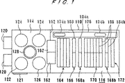
図1は、めっき装置を備えためっき設備の全体配置図を示す。このめっき設備は、基板の前処理、めっき及びめっきの後処理のめっき全工程を連続して自動的に行うようにしている。外装パネルを取付けた装置フレーム110の内部は、仕切板112によって、基板のめっき処理及びめっき液が付着した基板の処理を行うめっき空間116と、それ以外の処理、すなわちめっき液に直接には関わらない処理を行う清浄空間114に区分されている。めっき空間116と清浄空間114とを仕切る仕切板112で仕切られた仕切り部には、2つの基板ホルダ160(図2参照)を並列に配置して、この各基板ホルダ160との間で基板の脱着を行う、基板受渡し部としての基板脱着台162が備えられている。清浄空間114には、基板を収納した基板カセットを搭載するロード・アンロードポート120が接続されている。更に、装置フレーム110には、操作パネル121が備えられている。
Figure 1 shows an overall layout of a plating facility having a fit Kki device. This plating facility automatically performs all the steps of substrate pretreatment, plating, and post-plating plating continuously. The inside of the
清浄空間114の内部には、基板のオリエンテーションフラットやノッチなどの位置を所定方向に合わせるアライナ122と、めっき後の基板を洗浄し高速回転させてスピン乾燥させる2台の洗浄・乾燥装置124と、基板の前処理、この例では、基板の表面(被めっき面)に向けて純水を吹きかけることで、基板表面を純水で洗浄するとともに、純水で濡らして親水性を良くする水洗前処理を行う前処理装置126が、その四隅に位置して配置されている。更に、これらの各処理装置、つまりアライナ122、洗浄・乾燥装置124及び前処理装置126のほぼ中心に位置して、これらの各処理装置122,124,126、前記基板脱着台162及び前記ロード・アンロードポート120に搭載した基板カセットとの間で基板の搬送と受渡しを行う第1搬送ロボット128が配置されている。
Inside the
清浄空間114内に配置されたアライナ122、洗浄・乾燥装置124及び前処理装置126は、表面を上向きにした水平姿勢で基板を保持して処理するようになっている。搬送ロボット128は、表面を上向きにした水平姿勢で基板を保持して基板の搬送及び受渡しを行うようになっている。
The
めっき空間116内には、仕切板112側から順に、基板ホルダ160の保管及び一時仮置きを行うストッカ164、例えば基板の表面に形成したシード層表面の電気抵抗の大きい酸化膜を硫酸や塩酸などの薬液でエッチング除去する活性化処理装置166、基板の表面を純水で水洗する第1水洗装置168a、めっきを行うめっき装置170、第2水洗装置168b及びめっき後の基板の水切りを行うブロー装置172が順に配置されている。これらの装置の側方に位置して、2台の第2搬送ロボット174a,174bがレール176に沿って走行自在に配置されている。一方の第2搬送ロボット174aは、基板脱着台162とストッカ164との間で基板ホルダ160の搬送を行い、他方の第2搬送ロボット174bは、ストッカ164、活性化処理装置166、第1水洗装置168a、めっき装置170、第2水洗装置168b及びブロー装置172の間で基板ホルダ160の搬送を行う。
In the
各第2搬送ロボット174a,174bは、図2に示すように、鉛直方向に延びるボディ178と、このボディ178に沿って上下動自在でかつ軸心を中心に回転自在なアーム180を備えている。このアーム180に、基板ホルダ160を着脱自在に保持する基板ホルダ保持部182が2個並列に備えられている。基板ホルダ160は、表面を露出させ周縁部をシールした状態で基板Wを着脱自在に保持するように構成されている。
As shown in FIG. 2, each of the
ストッカ164、活性化処理装置166、水洗装置168a,168b及びめっき装置170は、基板ホルダ160の両端部に設けた外方に突出する突出部160aを引っ掛けて、基板ホルダ160を鉛直方向に吊り下げた状態で支持するようになっている。活性化処理装置166には、内部に薬液を保持する2個の活性化処理槽183が備えられている。図2に示すように、基板Wを装着した基板ホルダ160を鉛直状態で保持した第2搬送ロボット174bのアーム180を下降させ、必要に応じて、基板ホルダ160を活性化処理槽183の上端部に引っ掛けて吊下げ支持する。これにより、基板ホルダ160を基板Wごと活性化処理槽183内の薬液に浸漬させて活性化処理を行うように構成されている。
The
同様に、水洗装置168a,168bは、内部に純水を保持する各2個の水洗槽184a,184bをそれぞれ有し、めっき装置170には、内部にめっき液を保持する複数のめっき槽186を有している。水洗槽184a,184b及びめっき装置170は、前述と同様に、基板ホルダ160を基板Wごとこれらの水洗槽184a,184b内の純水またはめっき槽186内のめっき液に浸漬させることで、水洗処理やめっき処理が行われるように構成されている。基板Wを装着した基板ホルダ160を鉛直状態で保持した第2搬送ロボット174bのアーム180を下降させ、この基板ホルダ160に装着した基板Wにエアーや不活性ガスを吹きかけて、基板ホルダ160及び基板Wに付着した液体を吹き飛ばし、基板Wの水切り行う。このようにして、ブロー装置172は、ブロー処理を行うように構成されている。
Similarly, the rinsing
めっき装置170の各めっき槽186は、図3に示すように、内部にめっき液188を保持するように構成され、このめっき液188中に、基板ホルダ160で周縁部を水密的にシールし表面(被めっき面)を露出させて保持した基板Wを浸漬させる。
As shown in FIG. 3, each
めっき槽186の側方には、このめっき槽186の溢流堰200の上端をオーバフローしためっき液188を流すオーバフロー槽202が設けられている。オーバフロー槽202には、めっき液排出ライン204が連結されている。めっき液排出ライン204と下記のめっき液供給ライン218を結ぶめっき液循環ライン206に、循環ポンプ208、流量調節器210及びフィルタ212が設置されている。循環ポンプ208の駆動に伴ってめっき槽186内に供給されためっき液188は、めっき槽186の内部を満たし、しかる後、溢流堰200からオーバフローしてオーバフロー槽202内に流れ込み、循環ポンプ208に戻る。このようにして、めっき液は循環し、めっき液循環ライン206に沿って流れるめっき液188の流量は流量調節器210で調節される。
On the side of the
めっき槽186の内部には、基板Wの形状に沿った円板状のアノード214がアノードホルダ216に保持されて垂直に設置されている。このアノード214は、めっき槽186内にめっき液188を満たした時に、このめっき液188中に浸漬され、基板ホルダ160で保持してめっき槽186内の所定の位置に配置される基板Wと対面する。
Inside the
めっき槽186の内部には、アノード214とめっき槽186内の所定の位置に配置される基板ホルダ160との間に位置して、リング状のノズル配管220が配置されている。ノズル配管220は、めっき液供給ライン218に連結されている。ノズル配管220は、図4に示すように、基板Wの外形に沿った円形リング状に形成されており、このノズル配管220の円周方向に沿った所定の位置には、複数のめっき液噴射ノズル222が所定のピッチで設けられている。前述のようにして循環ポンプ208の駆動に伴って循環するめっき液188は、このめっき液噴射ノズル222から噴射されてめっき槽186内に供給される。
Inside the
この例では、ノズル配管220は、内部に開口部224aを有し、めっき槽186内をアノード側の区画と基板側の区画に仕切る矩形板状の固定板224に止め具226を介して固定されている。この開口部224aの大きさは、ノズル配管220の内径とほぼ同じか、やや小径に設定されている。ノズル配管220は、固定板224の基板側に位置して、開口部224aの周囲を囲むように配置されている。そして、めっき液噴射ノズル222は、このめっき液噴射ノズル222から噴射されるめっき液188が、基板ホルダ160で保持されてめっき槽186内の所定の位置に配置される基板Wのほぼ中央手前の合流点Pで合流する向きに配置されている。
In this example, the
リング状のノズル配管220に設けためっき液噴射ノズル222からめっき液188を噴射してめっき槽186内にめっき液188を供給して循環させる。この時に、めっき液噴射ノズル222から、基板Wの表面(被めっき面)に向けてめっき液188を噴射してめっき液188の強い噴流を当てることで、基板Wの表面全域における電位分布の均一性を乱すことを抑えつつ、めっき液188中のイオンを基板Wの表面に効率よく供給して、めっき膜質を劣化させることなく、めっき速度を高めることができる。しかも、めっき液噴射ノズル222から噴射させるめっき液188の流量および方向を、基板Wの表面近傍におけるめっき液188の流れがより均一となるように調整することで、基板Wの表面に形成されるめっき膜の膜厚の均一性を向上させることができる。
A
特に、めっき液噴射ノズル222から噴射されるめっき液188が、基板Wの表面のほぼ中央手前の合流点Pで合流するようにすることで、合流しためっき液188の流れは、基板Wの表面のほぼ中央に垂直に当たる流れとなり、その後、基板Wの表面に沿って外方に拡がる流れに方向を変える。これにより、めっき液188の基板Wの表面に衝突した後の流れがめっき液188の排出流れと干渉することを防止して、一定の連続した安定しためっき液188の流れを形成することができる。
In particular, the
ノズル配管220、めっき液噴射ノズル222及び固定板224は、例えば、PVC,PP,PEEK,PES,HT−PVC,PFA,PTFE,その他の樹脂系材料からなる誘電体から構成されている。これらの樹脂系材料は、めっき槽186内の電界分布が乱されてしまうことを防止するのに有効である。
めっき槽186の内部は、開口部224aを設けた固定板224で仕切られている。めっき液188は、この開口部224aを通過した後、オーバフロー槽202内に流入する。この結果、基板Wの全域に対する電位分布がより均一となる。
The inside of the
めっき装置170の操作は以下の通りである。先ず、めっき槽186の内部にめっき液188を満たしておく。そして、基板Wを保持した基板ホルダ160を下降させて、基板Wをめっき槽186内のめっき液188に浸漬させた所定の位置に配置する。この状態で、循環ポンプ208を駆動して、めっき液噴射ノズル222からめっき液188を基板Wの表面に向けて噴射してめっき槽186内に供給し、めっき液188を循環させる。同時に、導線228aを介してアノード214をめっき電源230の陽極に接続し、導線228bを介して基板Wをめっき電源230の陰極に接続し、これによって、基板Wの表面に金属を析出させて金属膜を形成する。
The operation of the
この時、前述のように、めっき液噴射ノズル222から、基板Wの表面(被めっき面)に向けてめっき液188を噴射してめっき液188の強い噴流を当てることで、めっき膜質を劣化させることなく、めっき速度を高めることができる。しかも、基板Wの表面近傍におけるめっき液188の流れがより均一となるように調整することで、基板Wの表面に形成されるめっき膜の膜厚の均一性を向上させることができる。
At this time, as described above, the plating film quality is deteriorated by spraying the plating liquid 188 from the plating
そして、めっき処理終了後、めっき電源230を基板W及びアノード214から切り離し、基板ホルダ160を基板Wごと上方に引き上げる。その後、基板Wの水洗及びリンス等の処理を行い、しかる後、めっき後の基板Wを次工程に搬送する。
Then, after the plating process is completed, the
このように構成しためっき設備による一連のバンプめっき処理を、図5A乃至5Eを参照して説明する。先ず、図5Aに示すように、基板Wの表面に給電層としてのシード層500を成膜し、このシード層500の全表面に、例えば高さHが20〜120μmのレジスト502を塗布する。その後、レジスト502の所定の位置に、例えば直径D1が20〜200μm程度の開口部502aを設ける。このようにして準備した基板Wを、その表面(被めっき面)を上にした状態で基板カセットに収容し、この基板カセットをロード・アンロードポート120に搭載する。
A series of bump plating processes by the plating equipment configured as described above will be described with reference to FIGS. 5A to 5E. First, as shown in FIG. 5A, a
このロード・アンロードポート120に搭載した基板カセットから、第1搬送ロボット128で基板Wを1枚取出し、アライナ122に載せてオリフラやノッチなどの位置を所定の方向に合わせる。このアライナ122で方向を合わせた基板Wを第1搬送ロボット128で前処理装置126に搬送する。この前処理装置126で、前処理液に純水を使用した前処理(水洗前処理)を施す。一方、ストッカ164内に鉛直姿勢で保管されていた基板ホルダ160を第2搬送ロボット174aで取出し、これを90゜回転させた水平状態にして基板脱着台162に2個並列に載置する。
One substrate W is taken out from the substrate cassette mounted on the load / unload
そして、前述の前処理(水洗前処理)を施した基板Wを、この基板脱着台162に載置された基板ホルダ160に周縁部をシールして装着する。そして、この基板Wを装着した基板ホルダ160を第2搬送ロボット174aで2基同時に把持し、上昇させた後、ストッカ164まで搬送する。基板ホルダ160を90゜回転させて垂直な状態となして下降させ、2基の基板ホルダ160をストッカ164に吊下げ保持(仮置き)する。この操作を順次繰返して、ストッカ164内に収容された基板ホルダ160に順次基板を装着し、ストッカ164の所定の位置に順次吊り下げ保持(仮置き)する。
Then, the substrate W that has been subjected to the above-mentioned pretreatment (pretreatment with water washing) is attached to the
一方、基板を装着しストッカ164に仮置きした基板ホルダ160を第2搬送ロボット174bで2基同時に把持し、上昇させた後、活性化処理装置166に搬送する。活性化処理槽183に入れた硫酸や塩酸などの薬液に基板を浸漬させてシード層表面の電気抵抗の大きい酸化膜をエッチングし、清浄な金属面を露出させる。基板を装着した基板ホルダ160を、前記と同様にして、第1水洗装置168aに搬送し、この水洗槽184aに入れた純水で基板の表面を水洗する。
On the other hand, two
水洗が終了した基板を装着した基板ホルダ160を、前記と同様にしてめっき装置170に搬送し、めっき槽186内のめっき液188に浸漬させた状態でめっき槽186に吊り下げ支持することで、基板Wの表面にめっきを施す。所定時間経過後、基板を装着した基板ホルダ160を第2搬送ロボット174bで再度保持してめっき槽186から引き上げ、これによって、めっき処理を終了する。
In the same manner as described above, the
そして、前述と同様にして、基板ホルダ160を第2水洗装置168bまで搬送し、この水洗槽184bに入れた純水に浸漬させて基板の表面を純水洗浄する。しかる後、この基板を装着した基板ホルダ160を、前記と同様にして、ブロー装置172に搬送する。ブロー装置172では、不活性ガスやエアーを基板に向けて吹き付けて、基板や基板ホルダ160に付着しためっき液や水滴を除去する。しかる後、この基板を装着した基板ホルダ160を、前記と同様にして、ストッカ164の所定の位置に戻して吊下げ保持する。
Then, in the same manner as described above, the
第2搬送ロボット174bは、上記作業を順次繰り返し、めっきが終了した基板を装着した基板ホルダ160を順次ストッカ164の所定の位置に戻して吊下げ保持する。
一方、めっき処理後の基板を装着しストッカ164に戻した基板ホルダ160を第2搬送ロボット174aで2基同時に把持し、前記と同様にして、基板脱着台162上に載置する。
The
On the other hand, the two
清浄空間114内に配置された第1搬送ロボット128は、この基板脱着台162上に載置された基板ホルダ160から基板を取出し、いずれかの洗浄・乾燥装置124に搬送する。そして、この洗浄・乾燥装置124で、表面を上向きにして水平に保持した基板を、純水等で洗浄し、高速回転させてスピン乾燥させる。しかる後、基板を第1搬送ロボット128でロード・アンロードポート120に搭載した基板カセットに戻して、一連のめっき処理を完了する。これにより、図5Bに示すように、レジスト502に設けた開口部502a内にめっき膜504を成長させた基板Wが得られる。
The
前述のようにしてスピン乾燥させた基板Wを、例えば温度が50〜60℃のアセトン等の溶剤に浸漬させて、図5Cに示すように、基板W上のレジスト502を剥離除去し、更に図5Dに示すように、めっき後の外部に露出する不要となったシード層500を除去する。次に、この基板Wに形成しためっき膜504をリフローさせることで、図5Eに示すように、表面張力で丸くなったバンプ506を形成する。更に、この基板Wを、例えば、100℃以上の温度でアニールして、バンプ506内の残留応力を除去する。
The substrate W spin-dried as described above is immersed in a solvent such as acetone having a temperature of 50 to 60 ° C., for example, and the resist 502 on the substrate W is peeled and removed as shown in FIG. 5C. As shown to 5D, the
この例によれば、めっき空間116内での基板の受渡しをめっき空間116内に配置した第2搬送ロボット174a,174bで、清浄空間114内での基板の受渡しを該清浄空間114内に配置した第1搬送ロボット128でそれぞれ行っている。従って、基板の前処理、めっき処理及びめっきの後処理の全めっき工程を連続して行うめっき処理装置の内部における基板周りの清浄度を向上させるとともに、めっき処理装置としてのスループットを向上させ、更にめっき処理装置の付帯設備の負荷を軽減して、めっき処理装置としてのより小型化を図ることができる。
According to this example, the
この例にあっては、めっき処理を行うめっき装置170として、フットプリントの小さいめっき槽186を有するものを使用している。従って、多数のめっき槽186を有するめっき装置170の更なる小型化を図り、工場付帯設備負荷をより軽減することができる。図1において2台設置されている洗浄・乾燥装置124の一方を、前処理装置に置き換えてもよい。
In this example, as the
図6は、他のめっき装置(電気めっき装置)を示す。図6に示すめっき装置の図3及び図4に示すめっき装置と異なる点は、基板Wを保持してめっき槽186の所定の位置に配置される基板ホルダ160とめっき液噴射ノズル222を備えたノズル配管220との間に、中央孔232aを有し、例えば肉厚が0.5〜10mm程度で、PVC,PP,PEEK,PES,HT−PVC,PFA,PTFE,その他の樹脂系材料からなる誘電体から構成される調整板(レギュレーションプレート)232を配置した点にある。図6に示すめっき装置の他の構成は、図3及び図4に示すめっき装置と同様である。
FIG. 6 shows another plating apparatus (electroplating apparatus). The plating apparatus shown in FIG. 6 differs from the plating apparatus shown in FIGS. 3 and 4 in that a
この例によれば、中央孔232aを有する調整板232を介して、めっき槽186内の電位分布を調節して、基板Wの周縁部に成膜されるめっき膜の膜厚が厚くなる防止することができる。
According to this example, the potential distribution in the
図7は、本発明の実施の形態のめっき装置(電気めっき装置)を示す。図7に示すめっき装置の図6に示すめっき装置と異なる点は、基板Wを保持してめっき槽186の所定の位置に配置される基板ホルダ160と調整板232との間に、下方に垂下する攪拌翼(パドル)234を備えた攪拌機構236を配置した点である。攪拌機構236は、攪拌翼234を基板ホルダ160で保持された基板Wと平行に往復動させてめっき液188を攪拌する。
Figure 7 shows the plating apparatus of implementation of the present invention (electroplating apparatus). The plating apparatus shown in FIG. 7 is different from the plating apparatus shown in FIG. 6 in that it hangs downward between the
この例によれば、めっき中に攪拌機構236を介して攪拌翼234を基板Wと平行に往復動させて、調整板232と基板Wとの間に位置するめっき液188を攪拌することで、基板Wの表面に沿っためっき液188の流れを、基板Wの表面の全面でより均等にして、基板Wの全面に亘ってより均一な膜厚のめっき膜を形成することができる。
According to this example, by reciprocating the
この例にあっては、攪拌翼234として、基板Wと対向する1辺に凹凸234aを形成したものを使用している。このように、攪拌翼234として、基板Wと対向する1辺に凹凸234aを形成したものを使用することで、下記の例のように、この攪拌翼234を往復運動させることにより、めっき液188中に多くの渦流を均一に且つ全般的に発生させることができる。これにより、基板Wの表面(被めっき面)に接するめっき液188の流れをより均一に且つ効果的に作用させて、基板Wの表面に膜厚の均一性がより良好な、即ちより均一な膜厚のめっき膜を形成することができる。
In this example, as the
図8は、本発明の他の実施の形態のめっき装置(電気めっき装置)を示す。図8に示すめっき装置の図7に示すめっき装置と異なる点は、ノズル配管220のアノード214と対面する側にもアノード214に向けてめっき液188を噴射する複数のめっき液噴射ノズル240を設け、このめっき液噴射ノズル240から噴射されるめっき液188の噴流がアノード214に当たるようにした点である。このように、アノード214にもめっき液188の噴流が当たるようにすることで、アノード214の溶解速度を促進させ、これによって、電気めっきにおけるめっき速度の高速化にアノード214の溶解を追従させることができる。
FIG. 8 shows a plating apparatus (electroplating apparatus) according to another embodiment of the present invention. The plating apparatus shown in FIG. 8 differs from the plating apparatus shown in FIG. 7 in that a plurality of plating
前述の各例は、固定板224を介してノズル配管220をめっき槽186の内部に固定して配置している。基板ホルダ160で保持した基板Wに対して、前後、左右または上下、またはこれらの組合せた方向にノズル配管を移動させてもよい。ノズル配管を基板の表面と平行な面に沿って円運動させたり、図9に示すように、ノズル配管220を首振り運動させたりしてもよい。これにより、めっき膜の膜厚均一性を更に向上させることができる。このことは、以下の各例においても同様である。
In each of the above-described examples, the
図10乃至図12は、更に他のめっき装置を示す。この例は、表面(被めっき面)を下向きにして保持した基板Wの該表面に無電解めっきを施すようにした無電解めっき装置である。 10 to 12, further showing the other plating apparatus. This example is an electroless plating apparatus in which electroless plating is performed on the surface of the substrate W held with the surface (surface to be plated) facing downward.
この無電解めっき装置は、内部にめっき液(無電解めっき液)300を保持する上方に開口しためっき槽302と、基板Wをその表面(被めっき面)を下向き(フェースダウン)にして着脱自在に水平に保持する上下動自在な基板ホルダ304を有している。めっき槽302の上部の周囲には、オーバフロー槽306が設けられ、このオーバフロー槽306には、めっき液排出ライン308が連結されている。めっき液供給ライン310に接続されたノズル配管312が、めっき槽302の内部の該めっき槽302に保持されるめっき液300に浸漬される位置に水平に配置されている。このノズル配管312の円周方向に沿った所定の位置には、めっき液噴射ノズル314が所定のピッチで設けられている。めっき液排出ライン308とめっき液供給ラインとがめっき液循環ラインで結ばれていることは、前述の例と同様である。
This electroless plating apparatus is detachable with a
このめっき液噴射ノズル314は、上方かつ内方(中央)に向けてめっき液300を噴射し、めっき液噴射ノズル314から噴射されためっき液300が基板Wの下面のほぼ中央手前で合流する向きに配置されている。
This plating
この例にあっては、基板ホルダ304で保持しめっき槽302の上端開口部を閉塞する位置に配置し、必要に応じて回転させた基板Wに向けてめっき液噴射ノズル314からめっき液300を噴射してめっき液300をめっき槽302内に供給し、めっき液300を循環させて無電解めっきを行う。この例は、めっき液噴射ノズル314から、基板Wの表面(被めっき面)に向けてめっき液300を噴射してめっき液300の強い噴流を当てることで、めっき膜質を劣化させることなく、めっき速度を高めることができ、しかも、基板Wの表面近傍におけるめっき液300の流れがより均一となるように調整することで、基板Wの表面に形成されるめっき膜の膜厚の均一性を向上させることができる。
In this example, the
図13に示すように、めっき液噴射ノズル314を有するセグメント316を、ジョイント318を介してリング状に連結して、ノズル配管312を構成するようにしてもよい。これにより、ノズル配管312の製作の便を図ることができる。このことは、前述の各例及び以下の例においても同様である。
As shown in FIG. 13, the
図14は、更に他のめっき装置を示す。この例は、表面(被めっき面)を下向きにして保持した基板Wの該表面に電気めっきを施すようにした電気めっき装置に適用したものである。図14に示すめっき装置の図10乃至図12に示すめっき装置と異なる点は、めっき液300として、電気めっき用のめっき液を使用するとともに、めっき槽302の底部におけるノズル配管312の下方位置に、平板状のアノード320を配置している。めっき液噴射ノズル314からめっき液300を基板Wの表面に向けて噴射しめっき槽302内に供給してめっき液を循環させる。同時に、導線322aを介してアノード320をめっき電源324の陽極に接続し、導線322bを介して基板Wをめっき電源324の陰極に接続し、これによって、めっき(電気めっき)を行う。
Figure 14 is a further show the other fit Kki device. This example is applied to an electroplating apparatus in which electroplating is performed on the surface of the substrate W held with the surface (surface to be plated) facing downward. The plating apparatus shown in FIG. 14 differs from the plating apparatus shown in FIGS. 10 to 12 in that a plating solution for electroplating is used as the
なお、前述の各例にあっては、被めっき材としての基板Wとして円形のものを使用し、ノズル配管220,312として、この基板Wの外形に沿った円形リング状のものを使用している。例えば、被めっき材として、矩形状の基板等を使用する場合には、図15に示すように、矩形リング状で、その四隅にめっき液噴射ノズル340を所定の向きに向けて設けたノズル配管342を使用するようにしてもよい。このノズル配管342は、矩形状の基板の全面により均一なめっき液の流れを形成することができる。
In each of the above-described examples, a circular substrate is used as the substrate W as the material to be plated, and circular nozzles along the outer shape of the substrate W are used as the
以上説明したように、本発明によれば、被めっき材上の電位分布の均一性を乱すことを抑えつつ、めっき液中のイオンを被めっき面に効率よく供給して、めっき膜質を劣化させることなく、めっき速度を高めることができる。しかも、めっき液噴射ノズルから噴射させるめっき液の流量および方向を、被めっき面近傍におけるめっき液の流れがより均一となるように調整することで、めっき膜の膜厚の均一性を向上させることができる。 As described above, according to the present invention, the ions in the plating solution are efficiently supplied to the surface to be plated while suppressing the uniformity of the potential distribution on the material to be plated, thereby degrading the quality of the plating film. Without increasing the plating rate. Furthermore, the uniformity of the thickness of the plating film can be improved by adjusting the flow rate and direction of the plating solution sprayed from the plating solution spray nozzle so that the flow of the plating solution in the vicinity of the surface to be plated becomes more uniform. Can do.
図16は、更に他のめっき装置(電気めっき装置)を示す。図16に示すように、めっき装置610は、内部にめっき液を保持するめっき槽611を有し、このめっき液中に、基板ホルダ612に保持された基板Wとアノードホルダ614に保持されたアノード615が垂直且つ平行に対向して配置される。基板Wは、導線616を通してめっき電源617の陰極に接続され、アノード615は、導線618を通してめっき電源617の陽極に接続される。
Figure 16 is a further show the other because Kki apparatus (electroplating apparatus). As shown in FIG. 16, the
基板Wとアノード615の間にめっき液を攪拌するための攪拌翼619を具備する攪拌機構620が設けられている。攪拌翼619は、めっき槽611の上部から底部に向かって略垂直に延びている。また、攪拌機構620は、攪拌翼619を基板Wに対して平行な方向に往復運動させる。攪拌翼619は、板状で、基板Wに対向する辺に三角形状の歯が連続する鋸歯状の凹凸619aが形成されている。めっき槽611には、この内部にめっき液を供給するめっき液供給口621と、内部のめっき液を排出するめっき液排出口622が設けられている。
A
この例によれば、基板Wに対向する1辺に凹凸619aが形成された攪拌翼619を、攪拌機構620により、基板Wに対して平行な方向に往復運動させることにより、めっき液中に多くの渦流が均一に且つ全般的に発生する。これにより、基板Wのめっき面に接するめっき液の流れが均一に且つ効果的に作用するため、基板Wの表面に膜厚の均一性が良好な、即ち均一な膜厚のめっき膜を形成することができる。
According to this example, the
上記例では、攪拌機構620の攪拌翼619の基板Wに対向する辺に、図17Aに示すように、三角形状の歯が連続する鋸歯状の凹凸619aを形成している。しかし、鋸歯状の凹凸は図17Aに示す例に限定されるものではなく、図17Bに示すように、矩形が連続する鋸歯状の凹凸619b、または図17Cに示すように、多数の細い溝が所定の間隔で形成されてなる凹凸619cでもよい。攪拌翼619の一辺に、三角形状の歯が連続する鋸歯状の凹凸619a、矩形が連続する鋸歯状の凹凸619b、或いは多数の細い溝が所定の間隔で形成されてなる凹凸619cを形成することにより、攪拌翼619の往復運動によって生じためっき液の流れは多くの渦流を均一に且つ全般的に発生させ、基板Wに接するめっき液の流れが均一に且つ効果的に作用するから、基板Wの表面により膜厚の均一性が良好なめっき膜を形成できる。
In the above example, sawtooth-shaped
図18は、更に他のめっき装置(電気めっき装置)を示す。図18に示すめっき装置において、図17と同一符号を付した部分は、図17と同一または相当部分を示す。このことは、他の図面においても同様である。図18に示すように、このめっき装置610の攪拌機構620は、鋸歯状の凹凸619aを形成した辺を基板Wに向けて配置した複数(図では2つ)の攪拌翼619を有している。攪拌機構620の攪拌翼619を基板Wに対して平行な方向に往復運動させることにより、めっき液中に多くの渦流がより均一に且つ全般的に発生して、基板Wに接するめっき液の流れが均一に且つ効果的に作用し、基板Wの表面(被めっき面)に膜厚の均一性が良好なめっき膜を形成できる。各攪拌翼619は、図17A乃至17Cに示す凹凸619a,619bまたは619cのいずれを有している。
Figure 18 is a further show the other because Kki apparatus (electroplating apparatus). In the plating apparatus shown in FIG. 18, the parts denoted by the same reference numerals as those in FIG. The same applies to other drawings. As shown in FIG. 18, the
図19Aは、他の攪拌機構の平面図で、図19Bは、他の攪拌機構の正面図である。図19A及び19Bに示すように、攪拌機構620は、複数(図19A及び19Bでは2個)の攪拌翼619,619を有し、各攪拌翼619,619は、夫々独立した駆動機構623,623で駆動される。各駆動機構623は、駆動モータ623−1、クランク623−2、案内部材623−3、駆動軸623−4及び軸受623−5を有している。攪拌翼619は、駆動軸623−4の先端部に取付けられている。各攪拌翼619,619は、図16に示すように、めっき槽611の上部から底部に向かって略垂直に延びる。
FIG. 19A is a plan view of another stirring mechanism, and FIG. 19B is a front view of the other stirring mechanism. As shown in FIGS. 19A and 19B, the
駆動モータ623−1を駆動して矢印Aに示すように回転させると、駆動モータ623−1の回転軸に一端を取付けられたクランク623−2の他端が案内部材623−3の案内溝623−3aに沿って往復運動する。クランク623−2の他端に連結された駆動軸623−4が軸受623−5に支持されて、矢印Bに示すように往復運動し、駆動軸623−4の先端部に取付けられた攪拌翼619が往復運動する。
When the drive motor 623-1 is driven and rotated as indicated by the arrow A, the other end of the crank 623-2 having one end attached to the rotation shaft of the drive motor 623-1 is the
上記のように、この例の攪拌機構620は、複数(図19A及び19Bでは2個)の攪拌翼619,619を具備し、各攪拌翼619,619は、夫々独立した駆動機構623,623で駆動される。複数の攪拌翼619,619を夫々独立した駆動機構623,623により駆動することにより、めっき液の攪拌分布状態を調整することができ、基板Wの表面(被めっき面)に均一性の良好な膜厚のめっき膜を形成できる。
As described above, the
図19A及び19Bに示す攪拌機構620の各駆動機構623に取付けられている攪拌翼619は同じ形状である。しかし、各攪拌翼の形状は、異なった形状でもよい。即ち、図20A及び20Bに示す攪拌機構では、ほぼ等しい長さの攪拌翼624,625を上下に配置し、各攪拌翼624,625をそれぞれ独立した駆動機構623,623で往復運動させるようにしている。各攪拌翼624,625の攪拌面が略一致するように、各攪拌翼624,625の1辺の先端624a,625aを一致させ、それぞれの攪拌翼624,625で上下の異なる領域のめっき液を攪拌できるようにしている。図21A及び21Bに示す攪拌機構では、長さの長い攪拌翼632と長さの短い攪拌翼634とを上下に配置して、各攪拌翼632,634をそれぞれ独立した駆動機構623で往復運動させるようにしている。そして各攪拌翼632,634の攪拌面が略一致するように、各攪拌翼632,634の1辺の先端632a,634aを一致させ、それぞれの攪拌翼632,634で上下の異なる領域のめっき液を攪拌できるようにしている。このように、異なった形状の攪拌翼を任意に選択して使用することにより、めっき液の攪拌分布状態を調整することができ、基板Wの表面に均一性の良好なめっき膜を形成できる。
The stirring
図22は、更に他の攪拌翼を示す。図22に示すように、攪拌翼626は、回動軸627に取付けられ、この回動軸627の回動により攪拌翼626の角度を変えることができる。このような攪拌翼626を、往復運動する駆動機構(例えば、図19A及び19Bに示す駆動機構623)に、例えば図23及び図24に示すように、複数個(図では3個)取付ける。図23に矢印Dで、図24に矢印Cでそれぞれ示すように、攪拌翼626を基板Wの表面(被めっき面)Waに対して平行に往復運動させ、攪拌翼626の運動方向の変化に合わせて回動軸627を回動させ、攪拌翼626の基板Wに対する角度を変化させる。
FIG. 22 shows still another stirring blade. As shown in FIG. 22, the
上記のように、攪拌機構の攪拌翼に図22に示す構成の攪拌翼626を用い、図23及び図24に示すように、攪拌翼626の運動方向の変化に合わせて攪拌翼626の基板Wに対する角度を変化させることにより、図23及び24に示すように、図23に矢印Fで、図24に矢印Eでそれぞれ示す流れがめっき液中に生じる。この攪拌翼626の動きによって生じるめっき液の流れを均一に且つ全般的に発生させ、めっき液が基板Wの被めっき面に、均一且つ効果的に作用させて、基板Wの表面に均一性の良好な膜厚のめっき膜を形成することができる。特に攪拌翼626を複数とすることにより、よりめっき液の流れが基板Wの表面Waの近傍に、均一に且つ全般的に発生するから、基板Wの表面Waに均一性の良好な膜厚のめっき膜を形成することができる。
As described above, the
図25は、更に他のめっき装置(電気めっき装置)を示す。図25に示すように、このめっき装置は、めっき槽611内に対向して配置された基板Wとアノード615の間に対向して配置された、攪拌翼628,628を具備する2個の攪拌機構629,630を有している。一方の攪拌機構629は基板Wに接近させて配置され、他方の攪拌機構630はアノード615に接近させて配置されている。基板W及びアノード615の双方に接するめっき液の流れを、一方の攪拌機構629の攪拌翼628(第1の攪拌翼)及び他方の攪拌機構630の攪拌翼628(第2の攪拌翼)を介して、より均一に且つ効果的に作用させることで、基板Wの表面に均一性の良好なめっき膜を形成できる。
Figure 25 is a further show the other because Kki apparatus (electroplating apparatus). As shown in FIG. 25, this plating apparatus includes two agitators each provided with agitating
図25に示す構成のめっき装置においては、攪拌機構629,630の攪拌翼628,628を、基板W及びアノード615に対向する辺に凹凸を設けていない攪拌翼628,628としている。しかし、図26に示すように、基板W及びアノード615に対向する辺に、図17Aに示すように、三角形状の歯が連続する鋸歯状の凹凸619aを形成した攪拌翼619を攪拌機構629,630に取付けてもよい。また、図17Bに示すように、矩形が連続する鋸歯状の凹凸619b、または図17Cに示すように、多数の細い溝が所定の間隔で形成されてなる凹凸619cを形成した攪拌翼619でもよい。
In the plating apparatus having the configuration shown in FIG. 25, the stirring
図25及び図26に示すめっき装置において、攪拌機構629,630は一体として矢印Gに示すように往復運動させても良いし、また、別々に往復運動させても良い。
In the plating apparatus shown in FIGS. 25 and 26, the stirring
以上本発明の実施の形態を説明したが、本発明は上記実の施形態に限定されるものではなく、特許請求の範囲、及び明細書と図面に記載された技術的思想の範囲内において種々の変形が可能である。明細書及び図面に直接記載がない何れの形状や構造や材質であっても、本願発明の作用・効果を奏する以上、本願発明の技術的思想の範囲内である。 Although the embodiments of the present invention have been described above, the present invention is not limited to the above-described embodiments, and various modifications can be made within the scope of the claims and the technical idea described in the specification and drawings. Can be modified. Any shape, structure, or material not directly described in the specification and drawings is within the scope of the technical idea of the present invention as long as the effects and advantages of the present invention are exhibited.
本発明は、基板の表面にめっきを施すめっき装置に係り、特に半導体ウェーハの表面に設けられたトレンチやビヤホール、レジスト開口部にめっき膜を形成したり、半導体ウェーハの表面にパッケージの電極と電気的に接続するバンプを形成したりするのに使用されるめっき装置に関する。 The present invention relates to a plating apparatus that performs plating on the surface of a substrate, and in particular, forms a plating film on a trench, a via hole, or a resist opening provided on the surface of a semiconductor wafer, The present invention relates to a plating apparatus used to form bumps to be connected to each other.
Claims (7)
前記めっき槽内のめっき液に浸漬させて配置されるアノードと、
被めっき材を保持して、被めっき材の被めっき面が前記アノードに対面する位置に、該被めっき材をめっき液に浸漬させつつ前記めっき槽内に配置するホルダと、
前記めっき槽の内部に該めっき槽内のめっき液に浸漬されるように配置され、前記ホルダで保持した被めっき材の被めっき面に向けてめっき液を噴射して前記めっき槽内にめっき液を供給する複数のめっき液噴射ノズルを有するリング状のノズル配管とを備え、
前記ノズル配管は、被めっき材の外形に沿った形状に形成され、
前記ノズル配管及び/または前記めっき液噴射ノズルは、電気絶縁材料で構成され、
前記ホルダで保持されて前記めっき槽内に配置される被めっき材と前記ノズル配管との間に位置して、めっき槽内のめっき液を攪拌する攪拌翼が被めっき材と平行に移動自在に配置されていることを特徴とする電気めっき装置。A plating tank for holding a plating solution;
An anode disposed by being immersed in a plating solution in the plating tank;
A holder for holding the material to be plated and placing the material to be plated in the plating tank while immersing the material to be plated in a plating solution at a position where the surface to be plated faces the anode,
The plating solution is disposed inside the plating tank so as to be immersed in the plating solution in the plating tank, and sprayed to the surface to be plated of the material to be plated held by the holder, and the plating solution is injected into the plating tank. A ring-shaped nozzle pipe having a plurality of plating solution injection nozzles for supplying
The nozzle pipe is formed in a shape along the outer shape of the material to be plated,
The nozzle pipe and / or the plating solution injection nozzle is made of an electrically insulating material ,
A stirring blade for agitating the plating solution in the plating tank, which is positioned between the material to be plated and held in the plating tank and held in the plating tank, is movable in parallel with the material to be plated. An electroplating apparatus characterized by being arranged .
Priority Applications (1)
| Application Number | Priority Date | Filing Date | Title |
|---|---|---|---|
| JP2006507663A JP4805141B2 (en) | 2003-03-11 | 2004-03-09 | Electroplating equipment |
Applications Claiming Priority (6)
| Application Number | Priority Date | Filing Date | Title |
|---|---|---|---|
| JP2003065476 | 2003-03-11 | ||
| JP2003065476 | 2003-03-11 | ||
| JP2003208315 | 2003-08-21 | ||
| JP2003208315 | 2003-08-21 | ||
| PCT/JP2004/003040 WO2004081261A2 (en) | 2003-03-11 | 2004-03-09 | Plating apparatus |
| JP2006507663A JP4805141B2 (en) | 2003-03-11 | 2004-03-09 | Electroplating equipment |
Related Child Applications (1)
| Application Number | Title | Priority Date | Filing Date |
|---|---|---|---|
| JP2010008438A Division JP5175871B2 (en) | 2003-03-11 | 2010-01-18 | Plating equipment |
Publications (3)
| Publication Number | Publication Date |
|---|---|
| JP2006519932A JP2006519932A (en) | 2006-08-31 |
| JP2006519932A5 JP2006519932A5 (en) | 2007-04-19 |
| JP4805141B2 true JP4805141B2 (en) | 2011-11-02 |
Family
ID=32992950
Family Applications (2)
| Application Number | Title | Priority Date | Filing Date |
|---|---|---|---|
| JP2006507663A Expired - Fee Related JP4805141B2 (en) | 2003-03-11 | 2004-03-09 | Electroplating equipment |
| JP2010008438A Expired - Fee Related JP5175871B2 (en) | 2003-03-11 | 2010-01-18 | Plating equipment |
Family Applications After (1)
| Application Number | Title | Priority Date | Filing Date |
|---|---|---|---|
| JP2010008438A Expired - Fee Related JP5175871B2 (en) | 2003-03-11 | 2010-01-18 | Plating equipment |
Country Status (7)
| Country | Link |
|---|---|
| US (2) | US7875158B2 (en) |
| EP (1) | EP1602127A2 (en) |
| JP (2) | JP4805141B2 (en) |
| KR (1) | KR101058917B1 (en) |
| CN (1) | CN101812711B (en) |
| TW (2) | TWI341875B (en) |
| WO (1) | WO2004081261A2 (en) |
Families Citing this family (48)
| Publication number | Priority date | Publication date | Assignee | Title |
|---|---|---|---|---|
| KR101186240B1 (en) | 2003-10-02 | 2012-09-27 | 가부시키가이샤 에바라 세이사꾸쇼 | Plating method and apparatus |
| KR101146525B1 (en) * | 2005-06-30 | 2012-05-25 | 엘지디스플레이 주식회사 | Jig for fixing display plate and Method thereof |
| NL1032540C2 (en) * | 2006-09-19 | 2008-03-20 | Meco Equip Eng | Device for the electrolytic deposition of material on a plate-shaped substrate. |
| JP4684979B2 (en) * | 2006-10-19 | 2011-05-18 | 本田技研工業株式会社 | Plating equipment |
| JP2008121062A (en) * | 2006-11-10 | 2008-05-29 | Ebara Corp | Plating device and plating method |
| DE102007026635B4 (en) * | 2007-06-06 | 2010-07-29 | Atotech Deutschland Gmbh | Apparatus for wet-chemical treatment of goods, use of a flow organ, method for installing a flow organ in the device and method for producing a wet-chemical treated goods |
| DE102007026633B4 (en) * | 2007-06-06 | 2009-04-02 | Atotech Deutschland Gmbh | Apparatus and method for the electrolytic treatment of plate-shaped goods |
| JP4942580B2 (en) * | 2007-08-20 | 2012-05-30 | 株式会社荏原製作所 | Current carrying belt for anode holder and anode holder |
| US8784636B2 (en) * | 2007-12-04 | 2014-07-22 | Ebara Corporation | Plating apparatus and plating method |
| US8177944B2 (en) | 2007-12-04 | 2012-05-15 | Ebara Corporation | Plating apparatus and plating method |
| JP4547016B2 (en) * | 2008-04-04 | 2010-09-22 | 東京エレクトロン株式会社 | Semiconductor manufacturing apparatus and semiconductor manufacturing method |
| JP5155755B2 (en) * | 2008-07-10 | 2013-03-06 | 株式会社荏原製作所 | Magnetic film plating apparatus and plating equipment |
| CN102803152B (en) * | 2009-05-29 | 2014-10-15 | H·布卢姆 | Apparatus and device for treating ballast water with acrolein |
| WO2011103214A1 (en) * | 2010-02-16 | 2011-08-25 | Cypress Semiconductor Corporation | Integrated shielding for wafer plating |
| US20110284385A1 (en) * | 2010-05-21 | 2011-11-24 | Pioneer Metal Finishing | Method and Apparatus For Anodizing Objects |
| KR101693217B1 (en) * | 2010-07-20 | 2017-01-05 | 주식회사 케이엠더블유 | Electroplating apparatus |
| US9222194B2 (en) * | 2010-08-19 | 2015-12-29 | International Business Machines Corporation | Rinsing and drying for electrochemical processing |
| KR101153537B1 (en) * | 2010-09-10 | 2012-06-11 | 삼성전기주식회사 | A plating device for printed circuit board a plating device for printed circuit board |
| JP6092653B2 (en) * | 2012-02-27 | 2017-03-08 | 株式会社荏原製作所 | Substrate cleaning apparatus and cleaning method |
| JP5788349B2 (en) * | 2012-03-19 | 2015-09-30 | 東京エレクトロン株式会社 | Plating processing apparatus, plating processing method, and storage medium |
| CN102660764B (en) * | 2012-05-25 | 2014-07-16 | 深圳顺络电子股份有限公司 | Inner cathode of electroplating basket |
| US8920616B2 (en) * | 2012-06-18 | 2014-12-30 | Headway Technologies, Inc. | Paddle for electroplating for selectively depositing greater thickness |
| JP5699253B2 (en) | 2012-07-02 | 2015-04-08 | 新日鐵住金株式会社 | Electroplating equipment |
| EP3117028B1 (en) * | 2014-03-11 | 2019-11-20 | Qualital Servizi S.r.l. | Plant and process for the anodizing treatment of products made of aluminium or its alloys |
| EP3144417B1 (en) | 2014-05-12 | 2019-09-18 | Yamamoto-ms Co., Ltd. | Plating apparatus and container bath |
| JP6411943B2 (en) * | 2014-05-26 | 2018-10-24 | 株式会社荏原製作所 | Substrate electrolytic treatment apparatus and paddle used for the substrate electrolytic treatment apparatus |
| GB2564894B (en) | 2017-07-27 | 2021-11-24 | Semsysco Gmbh | System for chemical and/or electrolytic surface treatment |
| JP6995544B2 (en) | 2017-09-20 | 2022-01-14 | 上村工業株式会社 | Surface treatment equipment and surface treatment method |
| KR20200073239A (en) * | 2017-10-20 | 2020-06-23 | 아루멕쿠스 피이 가부시키가이샤 | Surface treatment device |
| JP6966958B2 (en) * | 2018-03-01 | 2021-11-17 | 株式会社荏原製作所 | Plating equipment with paddles and paddles used to stir the plating solution |
| JP6790016B2 (en) * | 2018-04-10 | 2020-11-25 | 上村工業株式会社 | Surface treatment equipment, surface treatment method and paddle |
| JP6895927B2 (en) * | 2018-05-28 | 2021-06-30 | 三菱電機株式会社 | Semiconductor device manufacturing equipment and semiconductor device manufacturing method |
| KR102159043B1 (en) * | 2018-07-05 | 2020-09-23 | 주식회사 테토스 | wafer plating system |
| US11136688B1 (en) * | 2018-08-08 | 2021-10-05 | University Of Louisville Research Foundation, Inc. | Use of electropolishing for uniform surface treatment of metal components with complex external geometries |
| CN110888305A (en) * | 2018-09-07 | 2020-03-17 | 王彦智 | High-order negative photoresist stripping groove |
| JP7034880B2 (en) * | 2018-10-05 | 2022-03-14 | 株式会社荏原製作所 | Cleaning equipment, plating equipment equipped with this, and cleaning method |
| US10865496B2 (en) * | 2018-10-30 | 2020-12-15 | Taiwan Semiconductor Manufacturing Company, Ltd. | Plating apparatus and plating method |
| CN110735174B (en) * | 2019-03-22 | 2022-08-02 | Pyxis Cf私人有限公司 | Electroplating apparatus and method of operating the same |
| JP7169939B2 (en) * | 2019-05-27 | 2022-11-11 | 株式会社荏原製作所 | Wet substrate processing equipment |
| JP7383441B2 (en) * | 2019-10-07 | 2023-11-20 | 上村工業株式会社 | Surface treatment equipment, surface treatment method and paddle |
| CN211479988U (en) * | 2019-10-14 | 2020-09-11 | Pyxis Cf私人有限公司 | Wet processing equipment |
| CN112442725B (en) * | 2020-11-27 | 2024-05-24 | 京东方科技集团股份有限公司 | Electrochemical deposition apparatus set and electrochemical deposition method |
| KR102528900B1 (en) * | 2020-11-30 | 2023-05-04 | 주식회사 호진플라텍 | Plating apparatus including hybrid paddle that simultaneously circulates and stirs plating solution and removes air bubbles |
| JP2022111687A (en) * | 2021-01-20 | 2022-08-01 | 株式会社荏原製作所 | Short circuit detection method in plating apparatus, control method of plating apparatus, and plating apparatus |
| TWI784691B (en) * | 2021-08-27 | 2022-11-21 | 台灣先進系統股份有限公司 | Horizontal electroplating system |
| CN113798247B (en) * | 2021-09-28 | 2023-05-12 | 京东方科技集团股份有限公司 | Post-plating cleaning and air-drying mechanism, system, method and electrochemical deposition equipment |
| TWI813129B (en) * | 2022-01-06 | 2023-08-21 | 日月光半導體製造股份有限公司 | Chemical plating tank, chemical plating system and chemical plating method |
| CN116497302B (en) * | 2023-06-21 | 2023-11-24 | 山东华辉通信科技有限公司 | Galvanized equipment for rust prevention in communication iron tower processing |
Citations (8)
| Publication number | Priority date | Publication date | Assignee | Title |
|---|---|---|---|---|
| JPS5642976U (en) * | 1979-09-05 | 1981-04-18 | ||
| JPS59208092A (en) * | 1983-05-11 | 1984-11-26 | Hitachi Ltd | Plating method of noble metal |
| JPS61270889A (en) * | 1985-05-25 | 1986-12-01 | 三菱電機株式会社 | Plating apparatus |
| JPH10317199A (en) * | 1997-05-20 | 1998-12-02 | Hitachi Metals Ltd | Plating method and plating apparatus |
| JPH11181590A (en) * | 1997-12-17 | 1999-07-06 | Hitachi Ltd | Electroplating method and apparatus therefor |
| JP2002129381A (en) * | 2000-10-26 | 2002-05-09 | Hideyuki Kobayashi | Nozzle system for spouting plating solution capable of adjusting flow in plating equipment |
| JP2002173793A (en) * | 2000-12-01 | 2002-06-21 | Marunaka Kogyo Kk | Plating liquid spouting nozzle device for plating equipment |
| JP2002367998A (en) * | 2001-06-11 | 2002-12-20 | Ebara Corp | Semiconductor device and manufacturing method therefor |
Family Cites Families (18)
| Publication number | Priority date | Publication date | Assignee | Title |
|---|---|---|---|---|
| JPS53119227A (en) * | 1977-03-28 | 1978-10-18 | Sankuesuto Kk | Plating method |
| JPH05331679A (en) * | 1992-06-01 | 1993-12-14 | Sumitomo Metal Ind Ltd | Plating device |
| JPH0754189A (en) * | 1993-08-12 | 1995-02-28 | Matsushita Electric Ind Co Ltd | Electroplating device |
| US5421987A (en) | 1993-08-30 | 1995-06-06 | Tzanavaras; George | Precision high rate electroplating cell and method |
| JPH07210823A (en) | 1994-01-10 | 1995-08-11 | Fuji Elelctrochem Co Ltd | Forming method of magnetic pole of thin film magnetic head |
| US5683564A (en) | 1996-10-15 | 1997-11-04 | Reynolds Tech Fabricators Inc. | Plating cell and plating method with fluid wiper |
| US6071388A (en) | 1998-05-29 | 2000-06-06 | International Business Machines Corporation | Electroplating workpiece fixture having liquid gap spacer |
| US6395152B1 (en) * | 1998-07-09 | 2002-05-28 | Acm Research, Inc. | Methods and apparatus for electropolishing metal interconnections on semiconductor devices |
| KR100773165B1 (en) | 1999-12-24 | 2007-11-02 | 가부시키가이샤 에바라 세이사꾸쇼 | Semiconductor wafer processing apparatus and processing method |
| US6547937B1 (en) * | 2000-01-03 | 2003-04-15 | Semitool, Inc. | Microelectronic workpiece processing tool including a processing reactor having a paddle assembly for agitation of a processing fluid proximate to the workpiece |
| CN2405647Y (en) * | 2000-01-21 | 2000-11-15 | 华东师范大学 | Liquid agitating apparatus |
| US20020027080A1 (en) | 2000-03-17 | 2002-03-07 | Junichiro Yoshioka | Plating apparatus and method |
| KR100800531B1 (en) * | 2000-06-30 | 2008-02-04 | 가부시키가이샤 에바라 세이사꾸쇼 | Copper-plating liquid, plating method and plating apparatus |
| JP2002115096A (en) * | 2000-10-10 | 2002-04-19 | Applied Materials Inc | Plating apparatus |
| CN2471797Y (en) * | 2001-01-15 | 2002-01-16 | 太原风华高新技术有限公司 | Cyclic filtering agitator for electrolysis |
| US20030155185A1 (en) * | 2001-03-08 | 2003-08-21 | Masami Nomura | Elevator |
| US6875333B2 (en) * | 2002-02-14 | 2005-04-05 | Electroplating Engineers Of Japan Limited | Plating apparatus for wafer |
| US7390382B2 (en) * | 2003-07-01 | 2008-06-24 | Semitool, Inc. | Reactors having multiple electrodes and/or enclosed reciprocating paddles, and associated methods |
-
2004
- 2004-03-09 US US10/538,507 patent/US7875158B2/en not_active Expired - Fee Related
- 2004-03-09 EP EP04718745A patent/EP1602127A2/en not_active Withdrawn
- 2004-03-09 WO PCT/JP2004/003040 patent/WO2004081261A2/en active Application Filing
- 2004-03-09 JP JP2006507663A patent/JP4805141B2/en not_active Expired - Fee Related
- 2004-03-09 CN CN2010101447137A patent/CN101812711B/en not_active Expired - Fee Related
- 2004-03-09 KR KR1020057016780A patent/KR101058917B1/en active IP Right Grant
- 2004-03-10 TW TW093106296A patent/TWI341875B/en not_active IP Right Cessation
- 2004-03-10 TW TW100102767A patent/TWI498451B/en not_active IP Right Cessation
-
2010
- 2010-01-18 JP JP2010008438A patent/JP5175871B2/en not_active Expired - Fee Related
- 2010-12-13 US US12/966,297 patent/US8252167B2/en not_active Expired - Lifetime
Patent Citations (8)
| Publication number | Priority date | Publication date | Assignee | Title |
|---|---|---|---|---|
| JPS5642976U (en) * | 1979-09-05 | 1981-04-18 | ||
| JPS59208092A (en) * | 1983-05-11 | 1984-11-26 | Hitachi Ltd | Plating method of noble metal |
| JPS61270889A (en) * | 1985-05-25 | 1986-12-01 | 三菱電機株式会社 | Plating apparatus |
| JPH10317199A (en) * | 1997-05-20 | 1998-12-02 | Hitachi Metals Ltd | Plating method and plating apparatus |
| JPH11181590A (en) * | 1997-12-17 | 1999-07-06 | Hitachi Ltd | Electroplating method and apparatus therefor |
| JP2002129381A (en) * | 2000-10-26 | 2002-05-09 | Hideyuki Kobayashi | Nozzle system for spouting plating solution capable of adjusting flow in plating equipment |
| JP2002173793A (en) * | 2000-12-01 | 2002-06-21 | Marunaka Kogyo Kk | Plating liquid spouting nozzle device for plating equipment |
| JP2002367998A (en) * | 2001-06-11 | 2002-12-20 | Ebara Corp | Semiconductor device and manufacturing method therefor |
Also Published As
| Publication number | Publication date |
|---|---|
| CN101812711B (en) | 2011-11-16 |
| JP5175871B2 (en) | 2013-04-03 |
| EP1602127A2 (en) | 2005-12-07 |
| JP2006519932A (en) | 2006-08-31 |
| TWI341875B (en) | 2011-05-11 |
| TW200422429A (en) | 2004-11-01 |
| US8252167B2 (en) | 2012-08-28 |
| KR20050114226A (en) | 2005-12-05 |
| JP2010106369A (en) | 2010-05-13 |
| TW201131012A (en) | 2011-09-16 |
| WO2004081261A2 (en) | 2004-09-23 |
| CN101812711A (en) | 2010-08-25 |
| US20110073482A1 (en) | 2011-03-31 |
| WO2004081261B1 (en) | 2005-07-14 |
| US7875158B2 (en) | 2011-01-25 |
| WO2004081261A3 (en) | 2005-05-26 |
| KR101058917B1 (en) | 2011-08-23 |
| US20060113185A1 (en) | 2006-06-01 |
| TWI498451B (en) | 2015-09-01 |
Similar Documents
| Publication | Publication Date | Title |
|---|---|---|
| JP4805141B2 (en) | Electroplating equipment | |
| JP4434948B2 (en) | Plating apparatus and plating method | |
| JP4624738B2 (en) | Plating equipment | |
| US20060081478A1 (en) | Plating apparatus and plating method | |
| JP4365143B2 (en) | Method for stirring plating treatment liquid and plating treatment apparatus | |
| JP5281831B2 (en) | Method for forming conductive material structure | |
| JP5232844B2 (en) | Plating equipment | |
| CN101369533B (en) | Plating apparatus | |
| TWI518213B (en) | Method for forming conductive structure | |
| JP2004300462A (en) | Plating method and plating apparatus | |
| TWI726080B (en) | Manufacturing method of substrate and substrate | |
| US20060163058A1 (en) | Apparatus for plating a semiconductor wafer and plating solution bath used therein | |
| JP2006117966A (en) | Plating apparatus and plating method | |
| JP2004162129A (en) | Plating apparatus and plating method | |
| WO2023032191A1 (en) | Plating method and plating apparatus | |
| JP2013168679A (en) | Conductive material structure formation method | |
| JP2005226119A (en) | Substrate treatment method, plating method and plating apparatus | |
| JP2005281720A (en) | Wet treatment method and apparatus therefor | |
| JPH1192997A (en) | Method for filling liquid into minute hole, straight low melting point solder bump plating method and device therefor |
Legal Events
| Date | Code | Title | Description |
|---|---|---|---|
| A521 | Request for written amendment filed |
Free format text: JAPANESE INTERMEDIATE CODE: A523 Effective date: 20070305 |
|
| A621 | Written request for application examination |
Free format text: JAPANESE INTERMEDIATE CODE: A621 Effective date: 20070305 |
|
| A131 | Notification of reasons for refusal |
Free format text: JAPANESE INTERMEDIATE CODE: A131 Effective date: 20091117 |
|
| A521 | Request for written amendment filed |
Free format text: JAPANESE INTERMEDIATE CODE: A523 Effective date: 20100118 |
|
| A131 | Notification of reasons for refusal |
Free format text: JAPANESE INTERMEDIATE CODE: A131 Effective date: 20100525 |
|
| A521 | Request for written amendment filed |
Free format text: JAPANESE INTERMEDIATE CODE: A523 Effective date: 20100721 |
|
| A131 | Notification of reasons for refusal |
Free format text: JAPANESE INTERMEDIATE CODE: A131 Effective date: 20110426 |
|
| A521 | Request for written amendment filed |
Free format text: JAPANESE INTERMEDIATE CODE: A523 Effective date: 20110622 |
|
| TRDD | Decision of grant or rejection written | ||
| A01 | Written decision to grant a patent or to grant a registration (utility model) |
Free format text: JAPANESE INTERMEDIATE CODE: A01 Effective date: 20110719 |
|
| A01 | Written decision to grant a patent or to grant a registration (utility model) |
Free format text: JAPANESE INTERMEDIATE CODE: A01 |
|
| A61 | First payment of annual fees (during grant procedure) |
Free format text: JAPANESE INTERMEDIATE CODE: A61 Effective date: 20110810 |
|
| R150 | Certificate of patent or registration of utility model |
Free format text: JAPANESE INTERMEDIATE CODE: R150 Ref document number: 4805141 Country of ref document: JP Free format text: JAPANESE INTERMEDIATE CODE: R150 |
|
| FPAY | Renewal fee payment (event date is renewal date of database) |
Free format text: PAYMENT UNTIL: 20140819 Year of fee payment: 3 |
|
| R250 | Receipt of annual fees |
Free format text: JAPANESE INTERMEDIATE CODE: R250 |
|
| R250 | Receipt of annual fees |
Free format text: JAPANESE INTERMEDIATE CODE: R250 |
|
| R250 | Receipt of annual fees |
Free format text: JAPANESE INTERMEDIATE CODE: R250 |
|
| R250 | Receipt of annual fees |
Free format text: JAPANESE INTERMEDIATE CODE: R250 |
|
| R250 | Receipt of annual fees |
Free format text: JAPANESE INTERMEDIATE CODE: R250 |
|
| R250 | Receipt of annual fees |
Free format text: JAPANESE INTERMEDIATE CODE: R250 |
|
| R250 | Receipt of annual fees |
Free format text: JAPANESE INTERMEDIATE CODE: R250 |
|
| LAPS | Cancellation because of no payment of annual fees |