JP4775475B2 - Power converter - Google Patents
Power converter Download PDFInfo
- Publication number
- JP4775475B2 JP4775475B2 JP2009097559A JP2009097559A JP4775475B2 JP 4775475 B2 JP4775475 B2 JP 4775475B2 JP 2009097559 A JP2009097559 A JP 2009097559A JP 2009097559 A JP2009097559 A JP 2009097559A JP 4775475 B2 JP4775475 B2 JP 4775475B2
- Authority
- JP
- Japan
- Prior art keywords
- capacitor
- cooler
- semiconductor module
- terminal
- thermal contact
- Prior art date
- Legal status (The legal status is an assumption and is not a legal conclusion. Google has not performed a legal analysis and makes no representation as to the accuracy of the status listed.)
- Active
Links
Images


Classifications
-
- H—ELECTRICITY
- H05—ELECTRIC TECHNIQUES NOT OTHERWISE PROVIDED FOR
- H05K—PRINTED CIRCUITS; CASINGS OR CONSTRUCTIONAL DETAILS OF ELECTRIC APPARATUS; MANUFACTURE OF ASSEMBLAGES OF ELECTRICAL COMPONENTS
- H05K7/00—Constructional details common to different types of electric apparatus
- H05K7/20—Modifications to facilitate cooling, ventilating, or heating
- H05K7/2089—Modifications to facilitate cooling, ventilating, or heating for power electronics, e.g. for inverters for controlling motor
- H05K7/20927—Liquid coolant without phase change
-
- H—ELECTRICITY
- H05—ELECTRIC TECHNIQUES NOT OTHERWISE PROVIDED FOR
- H05K—PRINTED CIRCUITS; CASINGS OR CONSTRUCTIONAL DETAILS OF ELECTRIC APPARATUS; MANUFACTURE OF ASSEMBLAGES OF ELECTRICAL COMPONENTS
- H05K7/00—Constructional details common to different types of electric apparatus
- H05K7/20—Modifications to facilitate cooling, ventilating, or heating
- H05K7/2089—Modifications to facilitate cooling, ventilating, or heating for power electronics, e.g. for inverters for controlling motor
- H05K7/209—Heat transfer by conduction from internal heat source to heat radiating structure
-
- H—ELECTRICITY
- H05—ELECTRIC TECHNIQUES NOT OTHERWISE PROVIDED FOR
- H05K—PRINTED CIRCUITS; CASINGS OR CONSTRUCTIONAL DETAILS OF ELECTRIC APPARATUS; MANUFACTURE OF ASSEMBLAGES OF ELECTRICAL COMPONENTS
- H05K7/00—Constructional details common to different types of electric apparatus
- H05K7/14—Mounting supporting structure in casing or on frame or rack
- H05K7/1422—Printed circuit boards receptacles, e.g. stacked structures, electronic circuit modules or box like frames
- H05K7/1427—Housings
- H05K7/1432—Housings specially adapted for power drive units or power converters
- H05K7/14329—Housings specially adapted for power drive units or power converters specially adapted for the configuration of power bus bars
Landscapes
- Engineering & Computer Science (AREA)
- Microelectronics & Electronic Packaging (AREA)
- Physics & Mathematics (AREA)
- Thermal Sciences (AREA)
- Inverter Devices (AREA)
- Dc-Dc Converters (AREA)
Description
本発明は、半導体素子を内蔵した半導体モジュールと該半導体モジュールに接続されたコンデンサとを有する電力変換装置に関する。 The present invention relates to a power conversion device having a semiconductor module containing a semiconductor element and a capacitor connected to the semiconductor module.
インバータやコンバータ等の電力変換装置は、複数の半導体素子のスイッチング動作によって電力の変換を行っている。かかる電力変換装置において、例えば、直流電源から半導体モジュールへ供給される電流を平滑化するコンデンサが、半導体モジュールに電気的に接続されている。特許文献1には、このコンデンサと半導体モジュールとがバスバーを介して接続された電力変換装置が開示されている。
Power conversion devices such as inverters and converters convert power by switching operations of a plurality of semiconductor elements. In such a power conversion device, for example, a capacitor that smoothes a current supplied from a DC power supply to the semiconductor module is electrically connected to the semiconductor module.
しかしながら、上記従来の電力変換装置においては、半導体モジュールにおいて発熱した熱が接続部及びバスバーを通じてコンデンサへ伝わる。これにより、コンデンサが高温となり、劣化してしまうおそれがある。特に、高出力密度化に伴う電力変換装置の被制御電流の大電流化に伴い、半導体モジュールの発熱が大きくなる傾向にある。また、半導体素子の高耐熱化に伴い、より高温で半導体素子を使用する傾向にある。かかる状況の下、半導体モジュールの耐熱性が充分に確保されても、コンデンサの耐熱性が充分に確保されていないのが現状である。そのため、半導体モジュールからのコンデンサの受熱による劣化が電力変換装置における近年の重要課題となっている。 However, in the conventional power converter, the heat generated in the semiconductor module is transmitted to the capacitor through the connection portion and the bus bar. This may cause the capacitor to become hot and deteriorate. In particular, as the controlled current of the power converter increases with increasing output density, the heat generated by the semiconductor module tends to increase. In addition, with the increase in heat resistance of semiconductor elements, semiconductor elements tend to be used at higher temperatures. Under such circumstances, even if the heat resistance of the semiconductor module is sufficiently ensured, the heat resistance of the capacitor is not sufficiently ensured at present. Therefore, deterioration due to heat reception of the capacitor from the semiconductor module has become an important issue in recent years in the power converter.
本発明は、かかる従来の問題点に鑑みてなされたもので、コンデンサの温度上昇を低減した電力変換装置を提供しようとするものである。 The present invention has been made in view of such conventional problems, and an object of the present invention is to provide a power conversion device in which a rise in the temperature of a capacitor is reduced.
本発明は、半導体素子を内蔵する半導体モジュール又はリアクトルに電気的に接続されたコンデンサと、
上記半導体モジュール又は上記リアクトルに熱的に接触している冷却器とを有し、
上記コンデンサに設けられた複数のコンデンサ端子のうちの少なくとも一つは、上記冷却器と上記コンデンサとの間に配置された状態で上記冷却器に熱的に接触しており、
上記冷却器に熱的に接触した上記コンデンサ端子は、上記半導体モジュール又は上記リアクトルに接続される端子であると共に、上記半導体モジュール及び上記リアクトルとは異なる電子部品に接続される端子でもあり、
上記コンデンサ端子は、上記コンデンサに設けられた一対の電極にそれぞれ接続されており、
上記コンデンサ端子の少なくとも一つは、上記半導体モジュール又は上記リアクトルに接続される部位と、上記電極に接続される部位との間において、上記冷却器と上記コンデンサとの間に配置された状態で上記冷却器に熱的に接触していることを特徴とする電力変換装置にある(請求項1)。
The present invention includes a semiconductor module containing a semiconductor element or a capacitor electrically connected to a reactor;
A cooler in thermal contact with the semiconductor module or the reactor,
At least one of a plurality of capacitor terminals provided on the capacitor is in thermal contact with the cooler in a state of being disposed between the cooler and the capacitor ,
The capacitor terminal in thermal contact with the cooler is a terminal connected to the semiconductor module or the reactor, and is also a terminal connected to an electronic component different from the semiconductor module and the reactor,
The capacitor terminal is connected to a pair of electrodes provided on the capacitor,
At least one of the capacitor terminals is disposed between the cooler and the capacitor between the portion connected to the semiconductor module or the reactor and the portion connected to the electrode. The power converter is in thermal contact with the cooler (Claim 1).
本発明においては、上記冷却器が上記コンデンサ端子に熱的に接触している。これにより、コンデンサ端子の発熱を抑制すると共に、半導体モジュール又はリアクトルからコンデンサへの伝熱を抑制し、コンデンサの温度上昇を低減することができる。コンデンサ端子は、半導体モジュール又はリアクトルと直接あるいは接続導体等を介して接続されている。そして、コンデンサは、半導体モジュール又はリアクトルの熱を両者の接続部を介して受熱して温度上昇するため、この受熱経路あるいはこれと熱的に接続される部分の少なくとも一部であるコンデンサ端子を冷却器に熱的に接触させることにより、コンデンサが受熱する前に半導体モジュール又はリアクトルの熱を冷却器へ放熱することができる。そのため、コンデンサの受熱を抑制し、コンデンサの温度上昇を低減することができる。 In the present invention , the cooler is in thermal contact with the capacitor terminal. Thereby, while suppressing heat_generation | fever of a capacitor | condenser terminal, the heat transfer from a semiconductor module or a reactor to a capacitor | condenser can be suppressed, and the temperature rise of a capacitor | condenser can be reduced. Capacitor terminal, walk semiconductor module or reactor directly is connected via a connection conductor or the like. And since a capacitor | condenser receives the heat | fever of a semiconductor module or a reactor via both connection part and temperature rises, the capacitor | condenser terminal which is at least one part of this heat-receiving path | route or a part thermally connected with this is cooled. By bringing the capacitor into thermal contact, the heat of the semiconductor module or the reactor can be radiated to the cooler before the capacitor receives heat. Therefore, the heat reception of the capacitor can be suppressed, and the temperature rise of the capacitor can be reduced.
また、コンデンサ端子自身もそこを流れる電流によって発熱するが、上記冷却器が上記コンデンサ端子に熱的に接触していることにより、コンデンサ端子の温度上昇も抑制することができる。その結果、このコンデンサ端子の発熱による熱をコンデンサが受熱して温度上昇してしまうことも抑制ことができる。 In addition, the capacitor terminal itself generates heat due to the current flowing therethrough, but since the cooler is in thermal contact with the capacitor terminal, an increase in the temperature of the capacitor terminal can be suppressed. As a result, it is possible to prevent the capacitor from receiving heat due to the heat generated by the capacitor terminal and increasing the temperature.
また、上記冷却器に熱的に接触した上記コンデンサ端子は、上記冷却器と上記コンデンサとの間に配置されている。The capacitor terminal that is in thermal contact with the cooler is disposed between the cooler and the capacitor.
これにより、上記コンデンサ端子を大きな面積で上記冷却器に熱的に接触させることができるとともに、電力変換装置の小型化を容易に図ることができる。 Thereby, the capacitor terminal can be brought into thermal contact with the cooler with a large area, and the power converter can be easily downsized.
また、上記冷却器は、上記半導体モジュール又は上記リアクトルに熱的に接触している。The cooler is in thermal contact with the semiconductor module or the reactor.
これにより、一つの冷却器によって、上記半導体モジュール又は上記リアクトルと上記コンデンサ端子とを冷却することができるため、電力変換装置の小型化を容易に図ることができる。 Thereby, since the said semiconductor module or the said reactor, and the said capacitor | condenser terminal can be cooled with one cooler, size reduction of a power converter device can be achieved easily.
以上のごとく、本発明によれば、コンデンサの温度上昇を低減した電力変換装置を提供することができる。 As described above, according to the present invention, it is possible to provide a power conversion device in which the temperature rise of the capacitor is reduced.
本発明において、「熱的に接触」とは、上記半導体端子及び上記コンデンサ端子と、冷却器との間で熱交換可能な状態にあることを意味し、間に熱伝導性を有する絶縁材を介在させる場合なども含まれる。 In the present invention, “thermal contact” means that heat exchange is possible between the semiconductor terminal and the capacitor terminal and the cooler, and an insulating material having thermal conductivity is provided between them. The case where it interposes is also included.
また、上記コンデンサ端子の一部は、コンデンサ素子と共にポッティング材によって封止されており、該ポッティング材を介して上記冷却器に熱的に接触していてもよい(請求項3)。
この場合には、電力変換装置の小型化を容易に図ることができる。
A part of the capacitor terminals is sealed by potting material together with the capacitor element may be in thermal contact with the condenser through the potting material (claim 3).
In this case, the power converter can be easily downsized.
また、一対の上記コンデンサ端子は、少なくともその一部を互いに近接させていることが好ましい(請求項4)。
この場合には、半導体モジュールとコンデンサとの間に形成される回路におけるインダクタンスを低減することができる。これにより、半導体素子のスイッチング動作に起因するサージ電圧を低減することができる。
A pair of the capacitor terminals is preferably in close proximity to each other at least partially (claims 4).
In this case, the inductance in the circuit formed between the semiconductor module and the capacitor can be reduced. Thereby, the surge voltage resulting from the switching operation of the semiconductor element can be reduced.
また、上記冷却器は、内部に冷却媒体を流通させる冷媒流路を有することが好ましい(請求項5)。
この場合には、効果的にコンデンサの温度上昇を抑制することができる。
Moreover, it is preferable that the said cooler has a refrigerant | coolant flow path which distribute | circulates a cooling medium inside (Claim 5 ).
In this case, the temperature rise of the capacitor can be effectively suppressed.
また、上記冷却器は、上記冷媒流路を有する冷却管と、該冷却管に密着配置されるとともに内部に冷却媒体を流通させないヒートシンクとからなることが好ましい(請求項6)。
この場合には、上記冷却器の設計自由度が向上し、電力変換装置を構成する各部品の組み付け性を向上させることができる。
Further, the cooler, a cooling tube having the coolant channel is preferably made from a heat sink that does not flow through the cooling medium therein while being arranged close to the cooling tube (claim 6).
In this case, the design freedom of the cooler is improved, and the assembling property of each part constituting the power conversion device can be improved.
また、上記半導体モジュールは上記冷却管に熱的に接触し、上記コンデンサ端子の少なくとも一つは上記ヒートシンクに熱的に接触していることが好ましい(請求項7)。
この場合には、組み付け性に優れた電力変換装置を得ることができる。
Further, the semiconductor module is in thermal contact with the cooling tube, it is preferable that at least one of the capacitor terminals is in thermal contact with the heat sink (claim 7).
In this case, it is possible to obtain a power conversion device that is excellent in assemblability.
また、上記コンデンサ端子の一部は、コンデンサ素子と共にポッティング材によって封止されており、また、上記ヒートシンクは、上記ポッティング材にその一部が埋設されており、上記コンデンサ端子の一部は、上記ポッティング材を介して上記ヒートシンクに熱的に接触していることが好ましい(請求項8)。
この場合には、電力変換装置の小型化を容易に図ることができる。また、ポッティング材とコンデンサ端子、或いはポッティング材とヒートシンクとの間に隙間が形成され難く、放熱効率を向上させることができる。
Further, a part of the capacitor terminal is sealed together with a capacitor element by a potting material, and a part of the heat sink is embedded in the potting material, and a part of the capacitor terminal is it is preferable that through the potting material is in thermal contact with the heat sink (claim 8).
In this case, the power converter can be easily downsized. Further, it is difficult to form a gap between the potting material and the capacitor terminal or between the potting material and the heat sink, so that the heat radiation efficiency can be improved.
また、上記冷却器に熱的に接触した上記コンデンサ端子は、上記半導体端子又は上記リアクトルに接続される端子である。
これにより、半導体モジュール又はリアクトルからコンデンサへの受熱経路において、コンデンサ端子が冷却器に熱的に接触することとなるため、より効果的に、コンデンサが受熱する前に、半導体モジュール又はリアクトルの熱を冷却器へ放熱することができる。そのため、コンデンサの受熱をより効果的に抑制し、コンデンサの温度上昇を低減することができる。また、コンデンサ端子の発熱も抑制することができる。
Further, the capacitor terminals in thermal contact with the cooler, Ru Ah at terminal connected to the semiconductor terminal or the reactor.
As a result , in the heat receiving path from the semiconductor module or the reactor to the capacitor, the capacitor terminal is in thermal contact with the cooler. Therefore, the heat of the semiconductor module or the reactor is more effectively reduced before the capacitor receives heat. Heat can be dissipated to the cooler. Therefore, the heat receiving of the capacitor can be more effectively suppressed, and the temperature rise of the capacitor can be reduced. Further, heat generation at the capacitor terminal can be suppressed.
また、上記冷却器に熱的に接触した上記コンデンサ端子は、上記半導体モジュール及び上記リアクトルとは異なる電子部品に接続される端子でもある。
これにより、半導体モジュール又はリアクトルからのコンデンサの受熱経路に熱的に連続した部分を冷却器に熱的に接触させることとなるため、充分にコンデンサの温度上昇を抑制することができる。また、半導体モジュール又はリアクトルに接続するためのコンデンサ端子とは異なるコンデンサ端子を冷却器に熱的に接触させればよいため、設計自由度を向上させることができる。
Further, the capacitor terminals in thermal contact with the cooler More Ru in terminal connected to a different electronic component and the semiconductor module and the reactor.
Thereby , since the part thermally connected to the heat receiving path of the capacitor from the semiconductor module or the reactor is brought into thermal contact with the cooler, the temperature rise of the capacitor can be sufficiently suppressed. Moreover, since the capacitor terminal different from the capacitor terminal for connecting to the semiconductor module or the reactor may be brought into thermal contact with the cooler, the degree of freedom in design can be improved.
また、上記冷却器は、上記半導体モジュール及び上記リアクトルに熱的に接触していることが好ましい(請求項2)。
この場合には、一つの冷却器によって、上記半導体モジュール及び上記リアクトルと上記コンデンサ端子とを冷却することができるため、電力変換装置の小型化を容易に図ることができる。
Further, the cooler is preferably in thermal contact with the semiconductor module and the reactor (claim 2).
In this case, since the semiconductor module, the reactor, and the capacitor terminal can be cooled by a single cooler, the power converter can be easily downsized.
(参考例1)
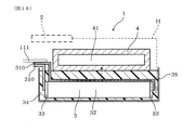
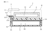
本発明の参考例にかかる電力変換装置につき、図1〜図3を用いて説明する。
本例の電力変換装置1は、図1、図2に示すごとく、半導体素子を内蔵すると共に少なくとも一対の半導体端子21を備えた半導体モジュール2と、該半導体モジュール2に電気的に接続されたコンデンサ3と、該コンデンサ3に設けられた複数のコンデンサ端子31のうちの少なくとも一つに熱的に接触する冷却器4とを有する。
( Reference Example 1 )
A power converter according to a reference example of the present invention will be described with reference to FIGS.
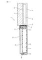
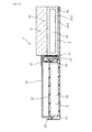
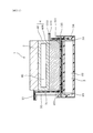
As shown in FIGS. 1 and 2, the
図1に示すごとく、冷却器4に熱的に接触したコンデンサ端子31は、冷却器4とコンデンサ3との間に配置されている。冷却器4は、半導体モジュール2にも熱的に接触している。冷却器4に熱的に接触したコンデンサ端子31は、半導体端子21に接続される端子である。
As shown in FIG. 1, the
コンデンサ3は、コンデンサ素子32と、該コンデンサ素子32の両端に形成されたメタリコン部からなる一対の電極33と、該一対の電極33に接続された一対のコンデンサ端子31と、コンデンサ素子32を封止するポッティング材34と、該ポッティング材34及びコンデンサ素子32を内部に収容する筐体35とからなる。一対のコンデンサ端子31は、その一部をポッティング材34から外部へ露出してなり、先端部において、半導体モジュール2の半導体端子21と接続されている。
一方のコンデンサ端子31は、ポッティング材34から露出した部分の一部を、コンデンサ3と冷却器4との間に配置し、冷却器4の主面42と熱的に面接触している。冷却器4とコンデンサ端子31との間には、熱伝導性に優れた絶縁材が介在している(図示略)。
上記ポッティング材34としては、例えばエポキシ樹脂等の熱伝導性に優れた熱硬化性樹脂を用いることができる。
One
As the
また、一対のコンデンサ端子31は、それぞれの一部(図1、図2の符号Bの領域)を互いに近接させている。各コンデンサ端子31は、平板状を呈しており、その主面同士を所定の間隔をもって対向配置させている。この所定の間隔は例えば0.6〜3mmとすることができる。また、対向、近接配置された一対のコンデンサ端子31の間には、絶縁紙等を介在させることもできる。
The pair of
半導体モジュール2は、冷却器4におけるコンデンサ3が配置された側と反対側の主面42に配置されている。すなわち、半導体モジュール2における放熱板を設けた面を冷却器4の主面42に熱的に接触配置する。このとき、必要に応じて、半導体モジュール2と冷却器4との間に、セラミック板、放熱グリスなどの熱伝導性に優れた絶縁材を配置する。
The
冷却器4は、アルミニウム又はその合金等の熱伝導性に優れた金属又は合金からなり、内部に冷却媒体を流通させる冷媒流路41を設けてなる。冷却媒体としては、例えば、水やアンモニア等の自然冷媒、エチレングリコール系の不凍液を混入した水、フロリナート等のフッ化炭素系冷媒、HCFC123、HFC134a等のフロン系冷媒、メタノール、アルコール等のアルコール系冷媒、アセトン等のケトン系冷媒等がある。
The
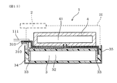
なお、本発明の電力変換装置1は、図3に示す回路構造を有するものとすることができる。すなわち、電力変換装置1は、直流電源52と三相交流の回転電機51との間において、直流電力を交流電力へ或いは交流電力を直流電力へ変換するインバータ部12と、直流電源51とインバータ部12との間において直流電圧を昇圧又は降圧する昇降圧コンバータ11とを有する。インバータ部12と昇降圧コンバータ11との間には、インバータ部へ供給される電流を平滑化するためのコンデンサ3が配置されている。また、インバータ部12は、複数の半導体モジュール2からなる。
In addition, the
この半導体モジュール2及びコンデンサ3の電力変換装置1における配置状態が、上述した配置状態(図1、図2)となっている。
なお、本例の電力変換装置1は、例えば、電気自動車やハイブリッド車等の動力源における電力変換に用いられる。
The arrangement state of the
In addition, the
次に、本例の作用効果につき説明する。
上記電力変換装置1においては、冷却器4がコンデンサ端子31に熱的に接触している。これにより、コンデンサ端子31の発熱を抑制すると共に、半導体モジュール2からコンデンサ3への伝熱を抑制し、コンデンサ3の温度上昇を低減することができる。コンデンサ端子31は、半導体モジュール2の半導体端子21と直接接続されている。そして、コンデンサ3は、半導体モジュール2の熱を両者の接続部を介して受熱して温度上昇するため、この受熱経路あるいはこれと熱的に接続される部分の少なくとも一部であるコンデンサ端子31を冷却器4に熱的に接触させることにより、コンデンサ3が受熱する前に半導体モジュール2の熱を冷却器4へ放熱することができる。そのため、コンデンサ3の受熱を抑制し、コンデンサ3の温度上昇を低減することができる。なお、半導体モジュール2からコンデンサ端子31を通じて冷却器4へ放熱される熱の移動を、図1における破線矢印Hにて表す。他の図においても同様に破線矢印Hにて熱の移動を表す。
Next, the function and effect of this example will be described.
In the
また、冷却器4がコンデンサ端子31に熱的に接触している。これにより、半導体モジュール2からコンデンサ3への伝熱を抑制し、コンデンサ3の温度上昇を低減することができる。コンデンサ端子31は、半導体モジュール2の半導体端子21と直接接続されている。そして、コンデンサ3は、半導体モジュール2の熱を両者の接続部を介して受熱して温度上昇するため、この受熱経路あるいはこれと熱的に接続される部分の少なくとも一部であるコンデンサ端子31を冷却器4に熱的に接触させることにより、コンデンサ3が受熱する前に半導体モジュール2の熱を冷却器4へ放熱することができる。そのため、コンデンサ3の受熱を抑制し、コンデンサ3の温度上昇を低減することができる。
The
また、コンデンサ端子31自身もそこを流れる電流によって発熱するが、冷却器4がコンデンサ端子31に熱的に接触していることにより、コンデンサ端子31の温度上昇も抑制することができる。その結果、このコンデンサ端子31の発熱による熱をコンデンサ3が受熱して温度上昇してしまうことも抑制ことができる。
Further, although the
また、一対のコンデンサ端子31は、その一部を互いに近接させているため、半導体モジュール2とコンデンサ3との間に形成される回路におけるインダクタンスを低減することができる。これにより、半導体素子のスイッチング動作に起因するサージ電圧を低減することができる。
また、冷却器4は、内部に冷却媒体を流通させる冷媒流路41を有するため、効果的にコンデンサ3の温度上昇を抑制することができる。
In addition, since a part of the pair of
Moreover, since the
以上のごとく、本例によれば、コンデンサの温度上昇を低減した電力変換装置を提供することができる。 As described above, according to this example, it is possible to provide a power conversion device in which the temperature rise of the capacitor is reduced.
(参考例2)
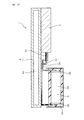
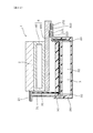
本例は、図4に示すごとく、一対のコンデンサ端子31の双方が冷却器4に熱的に接触した電力変換装置1の例である。
本例においては、一方のコンデンサ端子31は、参考例1と同様に、コンデンサ素子32との接続部と半導体モジュール2の半導体端子21との接続部との間の部分において、冷却器4に対して絶縁材を介して接触するとともにコンデンサ3と冷却器4との間に配置される。そして、他方のコンデンサ端子31は、コンデンサ素子32との接続部と半導体端子21との接続部との間の部分から分岐部311を設け、この分岐部311を冷却器4に対して絶縁材を介して接触させるとともにコンデンサ3と冷却器4との間に配置する。
その他は、参考例1と同様である。
( Reference Example 2 )
This example is an example of the
In this example, one
Others are the same as in Reference Example 1 .
なお、図4においては、一方のコンデンサ端子31と他方のコンデンサ端子31の分岐部311とが図面の奥行き方向に完全に重ならないように描かれているが、これは便宜上の記載方法であり、実際には一方のコンデンサ端子31と他方のコンデンサ端子31の分岐部311とは奥行き方向に重なっており、両者とも同様に冷却器4の主面42に絶縁材を介して接触している。他の図においても、これに準じた記載方法を採用している。
In FIG. 4, one
本例の場合には、上記他方のコンデンサ端子31からも半導体モジュール2の熱が冷却器4へ放熱され、コンデンサ3の受熱を低減することができる。そのため、より効果的に、コンデンサ端子31の発熱を抑制するとともに、コンデンサ3の受熱を低減して、コンデンサ3の温度上昇を抑制することができる。
その他、参考例1と同様の作用効果を有する。
In the case of this example, the heat of the
In addition, the same effects as those of Reference Example 1 are obtained.
(参考例3)
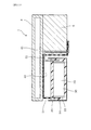
本例は、図5、図6に示すごとく、コンデンサ端子31をコンデンサ3のポッティング材34を介して冷却器4に熱的に接触させた電力変換装置1の例である。
コンデンサ端子31の一部は、コンデンサ素子32と共にポッティング材34によって封止されており、該ポッティング材34を介して冷却器4に熱的に接触している。
( Reference Example 3 )
This example is an example of the
A part of the
図5に示す電力変換装置1は、参考例1と同様に一方のコンデンサ端子31のみを冷却器4に熱的に接触させたものであり、図6に示す電力変換装置1は、参考例2と同様に一対のコンデンサ端子31の双方を冷却器4に熱的に接触させたものである。
その他は、参考例1と同様である。
Others are the same as in Reference Example 1 .
本例の場合には、電力変換装置1の小型化を容易に図ることができる。
その他、参考例1と同様の作用効果を有する。
In the case of this example, the
In addition, the same effects as those of Reference Example 1 are obtained.
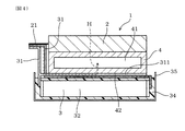
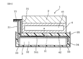
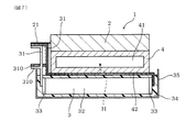
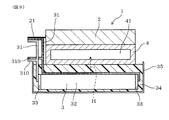
(実施例1)
本例は、図7〜図10に示すごとく、コンデンサ端子31、310を4本設けたコンデンサ3を用いた電力変換装置1の例である。
本例におけるコンデンサ3は、半導体モジュール2の半導体端子21に接続するための一対のコンデンサ端子31の他に、昇降圧コンデンサ11(図3参照)と接続するための一対のコンデンサ端子310を有する。このコンデンサ端子310は、コンデンサ素子32の一対の電極33にそれぞれ接続されている。すなわち、このコンデンサ端子310は、半導体モジュール2と接続するためのコンデンサ端子31と電気的に直接接続されている。
このような、4本のコンデンサ端子31、310を設けたコンデンサ3を用いた電力変換装置1においても、参考例1〜3と同様に本発明を適用することができる。
( Example 1 )
This example is an example of the
The
In the
図7、図9に示す電力変換装置1は、4本のコンデンサ端子31、310が同じ方向に突き出しており、一つのコンデンサ端子31が冷却器4に熱的に接触したものである。
図8、図10に示す電力変換装置1は、一対のコンデンサ端子31と他の一対のコンデンサ端子310とが互いに反対方向に突き出しており、2本のコンデンサ端子31が冷却器4に熱的に接触した例である。
また、図9、図10に示す電力変換装置1は、参考例3と同様に、コンデンサ端子31をコンデンサ3のポッティング材34を介して冷却器4に熱的に接触させた例である。
その他は、参考例1と同様である。
In the
In the
9 and 10 is an example in which the
Others are the same as in Reference Example 1 .
本例の場合にも、コンデンサの温度上昇を低減した電力変換装置を提供することができる。
すなわち、半導体モジュール2に直接接続されないコンデンサ端子310を新たに設けた場合にも、このコンデンサ端子310は直接半導体モジュール2に接続されたコンデンサ端子31と接続される。そのため、これらのコンデンサ端子31、310の何れの部分において冷却器4によって冷却しても、半導体モジュール2からコンデンサ3への伝熱を低減して、コンデンサ3の温度上昇を抑制することができる。
その他、参考例1と同様の作用効果を有する。
Also in the case of this example, the power converter device which reduced the temperature rise of the capacitor can be provided.
That is, when a
In addition, the same effects as those of Reference Example 1 are obtained.
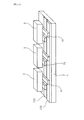
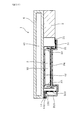
(参考例4)
本例は、図11、図12に示すごとく、コンデンサ3を冷却器4の主面42とは異なる端面43の方向に配置し、一対のコンデンサ端子31を冷却器4の端面43に熱的に接触させた電力変換装置1の例である。
また、一対のコンデンサ端子31は、コンデンサ3と冷却器4との間に配置される。
( Reference Example 4 )
In this example, as shown in FIGS. 11 and 12, the
Further, the pair of
図12に示すごとく、冷却器4の端面43に熱的に接触させたコンデンサ端子31を屈曲させるとともに延長した延設部312を設け、該延設部312において半導体モジュール2とは反対側の冷却器41の主面42にも熱的に接触させることもできる。
その他は、参考例1と同様である。
As shown in FIG. 12, an
Others are the same as in Reference Example 1 .
本例の場合にも、半導体モジュール2からコンデンサ3への伝熱を低減して、コンデンサ3の温度上昇を抑制することができる。
その他、参考例1と同様の作用効果を有する。
Also in the case of this example, the heat transfer from the
In addition, the same effects as those of Reference Example 1 are obtained.
(参考例5)
本例は、図13に示すごとく、半導体モジュール2を配置した冷却器4の主面42と同じ面にコンデンサ3を配置した電力変換装置1の例である。
一対のコンデンサ端子31は、半導体モジュール2を熱的に接触配置した冷却器4の主面42に、熱的に接触している。
その他は、参考例1と同様である。
本例の場合にも、参考例1と同様の作用効果を有する。
( Reference Example 5 )
This example is an example of the
The pair of
Others are the same as in Reference Example 1 .
Also in this example, it has the same effect as Reference Example 1 .
(参考例6)
本例は、図14〜図17に示すごとく、コンデンサ素子32の一対の電極33に、それぞれ、コンデンサ端子310の他に、半導体モジュール2の端子に接続されたバスバー(図示略)を直接接続した例である。
また、コンデンサ端子310を、冷却器4に熱的に接触させるとともにコンデンサ3と冷却器4との間に配置し、その他端を、例えば昇降圧コンバータ11(図3参照)の端子111と接続する。
図14〜図17においては、半導体モジュール2の具体的配置及び半導体端子21については省略してあるが、何らかの形で半導体端子21は、コンデンサ端子310と電気的及び熱的に接続されている。
( Reference Example 6 )
In this example, as shown in FIGS. 14 to 17, a bus bar (not shown) connected to the terminal of the
Further, the
14 to 17, the specific arrangement of the
なお、図14、図16に示す電力変換装置1は、一つのコンデンサ端子310が冷却器4に熱的に接触したものである。
図15、図17に示す電力変換装置1は、2本のコンデンサ端子310が冷却器4に熱的に接触したものである。
また、図16、図17に示す電力変換装置1は、参考例3と同様に、コンデンサ端子310をコンデンサ3のポッティング材34を介して冷却器4に熱的に接触させたものである。
In the
In the
Moreover, the
本例においては、半導体モジュール2の熱が、半導体モジュール2とコンデンサ3の電極33とを繋ぐバスバー(図示略)、電極33(メタリコン部)、コンデンサ端子310を介して、冷却器4に放熱されることとなる。
その他は、参考例1と同様である。
本例の場合にも、参考例1と同様の作用効果を有する。
In this example, the heat of the
Others are the same as in Reference Example 1 .
Also in this example, it has the same effect as Reference Example 1 .
なお、本例において、コンデンサ端子310は、昇降圧コンバータ11の端子111に限らず、インバータ部12の端子に接続されていてもよい。また、上記半導体モジュール2以外の発熱部品に接続されたバスバーをコンデンサ素子32の一対の電極33に直接接続した形態としてもよい。
In this example, the
(実施例2)
本例は、図18、図19に示すごとく、一対のコンデンサ端子310を、昇降圧コンバータ11に接続される入力バスバー131、132にそれぞれ接続し、入力バスバー131、132を冷却器4に熱的に接触させた電力変換装置1の例である。
入力バスバー131、132には、複数のコンデンサ3が並列接続される。また、これらのコンデンサ3には、それぞれ半導体モジュール2が接続される。
( Example 2 )
In this example, as shown in FIGS. 18 and 19, a pair of
A plurality of
コンデンサ3は、半導体モジュール2と反対側における冷却器4の主面42側に配置され、その主面42に入力バスバー131、132が、絶縁材14を介して固定されている。
その他は、参考例1と同様である。
本例の場合にも、参考例1と同様の作用効果を有する。
The
Others are the same as in Reference Example 1 .
Also in this example, it has the same effect as Reference Example 1 .
(参考例7)
本例は、図20に示すごとく、コンデンサ3を半導体モジュール2と同じ側における冷却器4の主面42に配置した例である。
本例においては、コンデンサ3の本体部も冷却器4に熱的に接触させている。
その他は、実施例2と同様である。
本例の場合にも、参考例1と同様の作用効果を有する。
( Reference Example 7 )
In this example, as shown in FIG. 20, the
In this example, the main body of the
Others are the same as in the second embodiment .
Also in this example, it has the same effect as Reference Example 1 .
(実施例3)
本例は、図21、図22に示すごとく、冷媒流路41を有する冷却管40と、該冷却管40に密着配置されるとともに内部に冷却媒体を流通させないヒートシンク400とからなる冷却器4を用いた電力変換装置1の例である。
半導体モジュール2は冷却管40に熱的に接触し、コンデンサ端子31はヒートシンク400に熱的に接触している。
ヒートシンク400は、アルミニウム又はその合金等、熱伝導性に優れた金属を用いて構成することができる。ヒートシンク400と冷却管40との間には、放熱グリスを介在させてもよい。
( Example 3 )
In this example, as shown in FIG. 21 and FIG. 22, a
The
The
図21に示す電力変換装置1は、コンデンサ端子31をポッティング材34を介してヒートシンク400に熱的に接触させたものである。コンデンサ端子31の一部は、コンデンサ素子32と共にポッティング材34によって封止されており、また、ヒートシンク400は、ポッティング材34にその一部が埋設されている。なお、この電力変換装置1においては、コンデンサ3の筐体35に、ヒートシンク400を支持するための支持部351を設けてある。これにより、ポッティング材34によってヒートシンク400の一部を埋設するにあたり、ヒートシンク400の位置決めを容易かつ正確に行うことができる。
In the
図22に示す電力変換装置1は、一対のコンデンサ端子31を、昇降圧コンバータ11に接続される入力バスバー131、132にそれぞれ接続し、入力バスバー131、132をヒートシンク400に熱的に接触させたものである。入力バスバー131、132は、絶縁材14を介してヒートシンク400に固定されている。
その他は、参考例1と同様である。
In the
Others are the same as in Reference Example 1 .
本例の場合には、冷却器4の設計自由度が向上し、電力変換装置1を構成する各部品の組み付け性を向上させることができる。
また、図21に示す電力変換装置1においては、予めコンデンサ3と一体化しておいたヒートシンク400を組み付け時に冷却管40と密着させることもできる。
その他、参考例1と同様の作用効果を有する。
In the case of this example, the design freedom of the
Moreover, in the
In addition, the same effects as those of Reference Example 1 are obtained.
(参考例8)
本例は、図23に示すごとく、リアクトル6と接続されるコンデンサ30において、そのコンデンサ端子31を冷却器4に熱的に接続した電力変換装置1の例である。
図3に示すごとく、電力変換装置1においては、直流電源52と昇降圧コンバータ11との間に、直流電源52のリプルを吸収するためのコンデンサ30が設けてある。このコンデンサ30の一方の端子は、昇降圧コンバータ11を構成するリアクトル6に接続されている。リアクトル6も発熱部品であって、リアクトル6からコンデンサ30が受熱するおそれがある。
( Reference Example 8 )
This example is an example of the
As shown in FIG. 3, in the
そこで、図23に示すごとく、リアクトル6と接続されるコンデンサ端子31を、冷却器4に熱的に接触させることにより、コンデンサ端子31の発熱を抑制するとともに、リアクトル6からのコンデンサ30の受熱を抑制し、コンデンサ30の温度上昇を低減することができる。
Therefore, as shown in FIG. 23, the
図23に示したような配置に限らず、参考例1〜7、実施例1〜3における半導体モジュール2をリアクトル6に置き換えたような種々の形態をとることができる。
また、半導体モジュール2もリアクトル6と共に同じ冷却器4に接触配置することもできる。
The present invention is not limited to the arrangement as shown in FIG. 23, but can take various forms in which the
Further, the
1 電力変換装置
2 半導体モジュール
21 半導体端子
3、30 コンデンサ
31 コンデンサ端子
4 冷却器
DESCRIPTION OF
Claims (8)
上記半導体モジュール又は上記リアクトルに熱的に接触している冷却器とを有し、
上記コンデンサに設けられた複数のコンデンサ端子のうちの少なくとも一つは、上記冷却器と上記コンデンサとの間に配置された状態で上記冷却器に熱的に接触しており、
上記冷却器に熱的に接触した上記コンデンサ端子は、上記半導体モジュール又は上記リアクトルに接続される端子であると共に、上記半導体モジュール及び上記リアクトルとは異なる電子部品に接続される端子でもあり、
上記コンデンサ端子は、上記コンデンサに設けられた一対の電極にそれぞれ接続されており、
上記コンデンサ端子の少なくとも一つは、上記半導体モジュール又は上記リアクトルに接続される部位と、上記電極に接続される部位との間において、上記冷却器と上記コンデンサとの間に配置された状態で上記冷却器に熱的に接触していることを特徴とする電力変換装置。 A semiconductor module containing a semiconductor element or a capacitor electrically connected to a reactor;
A cooler in thermal contact with the semiconductor module or the reactor,
At least one of a plurality of capacitor terminals provided on the capacitor is in thermal contact with the cooler in a state of being disposed between the cooler and the capacitor ,
The capacitor terminal in thermal contact with the cooler is a terminal connected to the semiconductor module or the reactor, and is also a terminal connected to an electronic component different from the semiconductor module and the reactor,
The capacitor terminal is connected to a pair of electrodes provided on the capacitor,
At least one of the capacitor terminals is disposed between the cooler and the capacitor between the portion connected to the semiconductor module or the reactor and the portion connected to the electrode. A power converter characterized by being in thermal contact with a cooler .
Priority Applications (2)
| Application Number | Priority Date | Filing Date | Title |
|---|---|---|---|
| JP2009097559A JP4775475B2 (en) | 2009-04-14 | 2009-04-14 | Power converter |
| US12/759,971 US8355244B2 (en) | 2009-04-14 | 2010-04-14 | Electric power converter |
Applications Claiming Priority (1)
| Application Number | Priority Date | Filing Date | Title |
|---|---|---|---|
| JP2009097559A JP4775475B2 (en) | 2009-04-14 | 2009-04-14 | Power converter |
Publications (2)
| Publication Number | Publication Date |
|---|---|
| JP2010252461A JP2010252461A (en) | 2010-11-04 |
| JP4775475B2 true JP4775475B2 (en) | 2011-09-21 |
Family
ID=42934212
Family Applications (1)
| Application Number | Title | Priority Date | Filing Date |
|---|---|---|---|
| JP2009097559A Active JP4775475B2 (en) | 2009-04-14 | 2009-04-14 | Power converter |
Country Status (2)
| Country | Link |
|---|---|
| US (1) | US8355244B2 (en) |
| JP (1) | JP4775475B2 (en) |
Families Citing this family (62)
| Publication number | Priority date | Publication date | Assignee | Title |
|---|---|---|---|---|
| JP4434181B2 (en) | 2006-07-21 | 2010-03-17 | 株式会社日立製作所 | Power converter |
| JP5702988B2 (en) * | 2010-01-29 | 2015-04-15 | 株式会社 日立パワーデバイス | SEMICONDUCTOR POWER MODULE, POWER CONVERSION DEVICE MOUNTED WITH THE SEMICONDUCTOR POWER MODULE, AND METHOD FOR MANUFACTURING SEMICONDUCTOR POWER MODULE WATER CHANNEL FORMING BODY |
| JP2012118516A (en) | 2010-11-11 | 2012-06-21 | Konica Minolta Business Technologies Inc | Method for forming hologram image, toner for electrostatic charge image development and hologram image forming apparatus |
| JP5351907B2 (en) * | 2011-01-13 | 2013-11-27 | アイシン・エィ・ダブリュ株式会社 | Semiconductor device |
| CN103354971B (en) | 2011-02-10 | 2016-01-20 | 三菱电机株式会社 | Power conversion device |
| JP5510432B2 (en) * | 2011-02-28 | 2014-06-04 | 株式会社豊田自動織機 | Semiconductor device |
| JP5644643B2 (en) * | 2011-04-08 | 2014-12-24 | 株式会社デンソー | Load drive device |
| US9516789B2 (en) * | 2011-05-05 | 2016-12-06 | Clean Wave Technologies, Inc. | Systems and methods for cooling of power electronic devices |
| FR2976762B1 (en) * | 2011-06-16 | 2016-12-09 | Valeo Systemes De Controle Moteur | ELECTRONIC POWER MODULE WITH INTEGRATED CAPACITY |
| JP5488540B2 (en) * | 2011-07-04 | 2014-05-14 | トヨタ自動車株式会社 | Semiconductor module |
| US20130019891A1 (en) * | 2011-07-21 | 2013-01-24 | Maggie Cheung | Device and method for heating hair curlers |
| JP5724811B2 (en) * | 2011-10-06 | 2015-05-27 | 株式会社デンソー | Power converter |
| JP5725367B2 (en) * | 2011-12-16 | 2015-05-27 | 株式会社デンソー | Discharge and noise reduction device for power converter |
| JP5733234B2 (en) * | 2012-02-15 | 2015-06-10 | 株式会社デンソー | Power converter |
| EP2637489B1 (en) * | 2012-03-06 | 2018-01-24 | ABB Schweiz AG | Electrical power circuit assembly |
| JP2013192367A (en) * | 2012-03-14 | 2013-09-26 | Hitachi Automotive Systems Ltd | Electric power conversion apparatus |
| CN103368359B (en) * | 2012-04-11 | 2016-04-13 | 台达电子工业股份有限公司 | Converter power unit and its busbar |
| DE102012206271A1 (en) * | 2012-04-17 | 2013-10-17 | Semikron Elektronik Gmbh & Co. Kg | Liquid-cooled arrangement with storable power semiconductor modules and at least one capacitor device and power semiconductor module for this purpose |
| JP5699995B2 (en) * | 2012-07-02 | 2015-04-15 | 株式会社デンソー | Power converter |
| KR101614669B1 (en) * | 2012-08-27 | 2016-04-21 | 미쓰비시덴키 가부시키가이샤 | Electric power semiconductor device |
| JP5738817B2 (en) | 2012-09-14 | 2015-06-24 | 日立オートモティブシステムズ株式会社 | Power converter |
| JP6039356B2 (en) * | 2012-10-22 | 2016-12-07 | 日立オートモティブシステムズ株式会社 | Power converter |
| JP5932605B2 (en) * | 2012-10-30 | 2016-06-08 | 日立オートモティブシステムズ株式会社 | Power converter |
| JP5734364B2 (en) * | 2012-11-22 | 2015-06-17 | 株式会社デンソー | Power converter |
| US9445532B2 (en) * | 2013-05-09 | 2016-09-13 | Ford Global Technologies, Llc | Integrated electrical and thermal solution for inverter DC-link capacitor packaging |
| JP2014229782A (en) * | 2013-05-23 | 2014-12-08 | 株式会社豊田自動織機 | Semiconductor device and manufacturing method of the same |
| JP6075227B2 (en) * | 2013-06-27 | 2017-02-08 | 株式会社デンソー | Power converter |
| JP6180857B2 (en) * | 2013-09-06 | 2017-08-16 | 日立オートモティブシステムズ株式会社 | Power converter |
| KR101545410B1 (en) * | 2013-12-31 | 2015-08-21 | 현대모비스 주식회사 | Capacitor module, Method for manufacturing the same, and Inverter for vehicle having the same |
| WO2015107870A1 (en) * | 2014-01-16 | 2015-07-23 | パナソニックIpマネジメント株式会社 | Semiconductor device |
| JP6443211B2 (en) * | 2014-10-31 | 2018-12-26 | 株式会社デンソー | Power converter |
| JP5925863B2 (en) * | 2014-11-07 | 2016-05-25 | 日立オートモティブシステムズ株式会社 | Power converter |
| JP6435905B2 (en) | 2015-02-13 | 2018-12-12 | 株式会社デンソー | Power converter |
| JP6435906B2 (en) * | 2015-02-13 | 2018-12-12 | 株式会社デンソー | Power converter |
| JP6500512B2 (en) * | 2015-03-06 | 2019-04-17 | 日産自動車株式会社 | Power converter |
| US9584061B1 (en) | 2015-09-17 | 2017-02-28 | Toyota Motor Engineering & Manufacturing North America, Inc. | Electric drive systems including smoothing capacitor cooling devices and systems |
| DE102015219643A1 (en) * | 2015-10-09 | 2017-04-27 | Conti Temic Microelectronic Gmbh | Electric motor-inverter |
| EP3370255A4 (en) * | 2015-10-28 | 2019-06-26 | Mitsubishi Electric Corporation | POWER CONVERSION DEVICE |
| FR3046904B1 (en) * | 2016-01-20 | 2018-03-02 | Valeo Systemes De Controle Moteur | ELECTRICAL EQUIPMENT, IN PARTICULAR FOR MOTOR VEHICLE |
| JP6214710B2 (en) * | 2016-04-05 | 2017-10-18 | 三菱電機株式会社 | Power converter |
| KR102131684B1 (en) * | 2016-04-28 | 2020-07-08 | 닛산 지도우샤 가부시키가이샤 | Vehicle-mounted power converter |
| DE102016216237A1 (en) * | 2016-08-29 | 2018-03-01 | Bayerische Motoren Werke Aktiengesellschaft | Capacitor assembly |
| JP6631463B2 (en) * | 2016-10-17 | 2020-01-15 | 株式会社デンソー | Power converter |
| US10811989B2 (en) * | 2017-03-30 | 2020-10-20 | Aisin Aw Co., Ltd. | Inverter unit |
| JP6897311B2 (en) * | 2017-05-23 | 2021-06-30 | 富士電機株式会社 | Power converter |
| JP6992327B2 (en) * | 2017-08-29 | 2022-01-13 | 富士電機株式会社 | Inverter device |
| US10850623B2 (en) * | 2017-10-30 | 2020-12-01 | Sf Motors, Inc. | Stacked electric vehicle inverter cells |
| JP7218828B2 (en) * | 2018-03-16 | 2023-02-07 | 富士電機株式会社 | power converter |
| JP7052447B2 (en) * | 2018-03-16 | 2022-04-12 | 富士電機株式会社 | Power converter |
| DE102018111630A1 (en) * | 2018-05-15 | 2019-11-21 | Valeo Siemens Eautomotive Germany Gmbh | Power conversion device for a vehicle and vehicle |
| WO2019234467A1 (en) * | 2018-06-08 | 2019-12-12 | 日産自動車株式会社 | Power converter |
| JP6915633B2 (en) * | 2018-07-25 | 2021-08-04 | 株式会社デンソー | Power converter |
| FR3085577B1 (en) | 2018-09-04 | 2020-10-02 | Valeo Siemens Eautomotive France Sas | CAPACITIVE BLOCK INCLUDING A THERMAL SINK |
| FR3091141B1 (en) * | 2018-12-21 | 2021-06-25 | Valeo Siemens Eautomotive France Sas | Electrical assembly of an electrical connection bar and a cooling module |
| US11282640B2 (en) * | 2019-04-12 | 2022-03-22 | Karma Automotive Llc | DC link capacitor cooling system |
| JP7243582B2 (en) * | 2019-11-08 | 2023-03-22 | 株式会社デンソー | power converter |
| US11527357B2 (en) | 2020-04-10 | 2022-12-13 | Hamilton Sundstrand Corporation | Busbar with tailored perforation sizes to provide thermal path |
| JP7628845B2 (en) * | 2021-03-16 | 2025-02-12 | 株式会社デンソー | Power Conversion Equipment |
| US12556106B2 (en) * | 2021-08-31 | 2026-02-17 | Hitachi Astemo, Ltd. | Electric power conversion device |
| DE102022123893A1 (en) | 2022-09-19 | 2024-03-21 | Dr. Ing. H.C. F. Porsche Aktiengesellschaft | Pulse inverter and method for cooling a pulse inverter |
| JP7343026B1 (en) | 2022-10-17 | 2023-09-12 | 富士電機株式会社 | power converter |
| JP2024073276A (en) * | 2022-11-17 | 2024-05-29 | 株式会社デンソー | Capacitor Device |
Family Cites Families (18)
| Publication number | Priority date | Publication date | Assignee | Title |
|---|---|---|---|---|
| JP3849838B2 (en) | 2000-02-17 | 2006-11-22 | 富士電機システムズ株式会社 | Winding foil electrode capacitor |
| JP4055042B2 (en) * | 2000-06-29 | 2008-03-05 | 株式会社デンソー | Inverter device |
| JP3646049B2 (en) | 2000-07-18 | 2005-05-11 | 東芝三菱電機産業システム株式会社 | Power converter |
| JP2004296958A (en) * | 2003-03-28 | 2004-10-21 | Hitachi Ltd | Capacitor and power conversion device using the same |
| JP2005332863A (en) * | 2004-05-18 | 2005-12-02 | Denso Corp | Power stack |
| US7210304B2 (en) * | 2005-02-09 | 2007-05-01 | General Motors Corporation | Cooling arrangements for integrated electric motor-inverters |
| JP2006332597A (en) * | 2005-04-28 | 2006-12-07 | Denso Corp | Semiconductor cooling unit |
| JP4453026B2 (en) * | 2005-09-20 | 2010-04-21 | アイシン・エィ・ダブリュ株式会社 | Inverter device |
| US20070165376A1 (en) * | 2006-01-17 | 2007-07-19 | Norbert Bones | Three phase inverter power stage and assembly |
| JP4857017B2 (en) * | 2006-04-27 | 2012-01-18 | 日立オートモティブシステムズ株式会社 | Power converter |
| JP2008061282A (en) * | 2006-08-29 | 2008-03-13 | Hitachi Ltd | Power converter |
| JP4973125B2 (en) * | 2006-10-31 | 2012-07-11 | 株式会社明電舎 | Inverter snubber capacitor and cooling structure of snubber circuit |
| JP4751810B2 (en) * | 2006-11-02 | 2011-08-17 | 日立オートモティブシステムズ株式会社 | Power converter |
| JP2008148530A (en) * | 2006-12-13 | 2008-06-26 | Toshiba Corp | Inverter device |
| JP4683003B2 (en) * | 2007-03-30 | 2011-05-11 | 株式会社デンソー | Power module and power converter using the same |
| JP4819071B2 (en) * | 2008-02-06 | 2011-11-16 | 本田技研工業株式会社 | Electric vehicle and cooling method for DC / DC converter for vehicle |
| JP4580997B2 (en) * | 2008-03-11 | 2010-11-17 | 日立オートモティブシステムズ株式会社 | Power converter |
| US20100244585A1 (en) * | 2009-03-26 | 2010-09-30 | General Electric Company | High-temperature capacitors and methods of making the same |
-
2009
- 2009-04-14 JP JP2009097559A patent/JP4775475B2/en active Active
-
2010
- 2010-04-14 US US12/759,971 patent/US8355244B2/en not_active Expired - Fee Related
Also Published As
| Publication number | Publication date |
|---|---|
| US20100259898A1 (en) | 2010-10-14 |
| US8355244B2 (en) | 2013-01-15 |
| JP2010252461A (en) | 2010-11-04 |
Similar Documents
| Publication | Publication Date | Title |
|---|---|---|
| JP4775475B2 (en) | Power converter | |
| JP5120221B2 (en) | Power converter | |
| JP5714077B2 (en) | Cooling device for connecting conductor and power conversion device using the same | |
| JP6932225B1 (en) | Power converter | |
| JP6457895B2 (en) | Capacitor module | |
| JPWO2013140502A1 (en) | Power converter | |
| JP6500756B2 (en) | Power converter | |
| JP6180857B2 (en) | Power converter | |
| EP3641121A1 (en) | Cooling structure of power conversion device | |
| JP2013146179A (en) | Electric power conversion apparatus | |
| JP5712750B2 (en) | Power converter | |
| JP6158051B2 (en) | Power converter | |
| CN111279601A (en) | Power conversion device | |
| JP5326646B2 (en) | Power converter | |
| JP7319945B2 (en) | power converter | |
| WO2019244502A1 (en) | Electric power converter | |
| JP6144600B2 (en) | Power converter | |
| JP2004274959A (en) | Power converter | |
| JP5447191B2 (en) | Power converter | |
| JP6440779B1 (en) | Power converter | |
| JP2016165179A (en) | Power converter | |
| JP7134305B1 (en) | power converter | |
| JP2011250607A (en) | Power conversion equipment | |
| CN223110359U (en) | Inverter with cooling device | |
| KR102877586B1 (en) | Power Conversion System |
Legal Events
| Date | Code | Title | Description |
|---|---|---|---|
| A521 | Request for written amendment filed |
Free format text: JAPANESE INTERMEDIATE CODE: A523 Effective date: 20100111 |
|
| A621 | Written request for application examination |
Free format text: JAPANESE INTERMEDIATE CODE: A621 Effective date: 20100903 |
|
| A977 | Report on retrieval |
Free format text: JAPANESE INTERMEDIATE CODE: A971007 Effective date: 20110214 |
|
| A131 | Notification of reasons for refusal |
Free format text: JAPANESE INTERMEDIATE CODE: A131 Effective date: 20110222 |
|
| A521 | Request for written amendment filed |
Free format text: JAPANESE INTERMEDIATE CODE: A523 Effective date: 20110419 |
|
| TRDD | Decision of grant or rejection written | ||
| A01 | Written decision to grant a patent or to grant a registration (utility model) |
Free format text: JAPANESE INTERMEDIATE CODE: A01 Effective date: 20110531 |
|
| A01 | Written decision to grant a patent or to grant a registration (utility model) |
Free format text: JAPANESE INTERMEDIATE CODE: A01 |
|
| A61 | First payment of annual fees (during grant procedure) |
Free format text: JAPANESE INTERMEDIATE CODE: A61 Effective date: 20110613 |
|
| R151 | Written notification of patent or utility model registration |
Ref document number: 4775475 Country of ref document: JP Free format text: JAPANESE INTERMEDIATE CODE: R151 |
|
| FPAY | Renewal fee payment (event date is renewal date of database) |
Free format text: PAYMENT UNTIL: 20140708 Year of fee payment: 3 |
|
| R250 | Receipt of annual fees |
Free format text: JAPANESE INTERMEDIATE CODE: R250 |
|
| R250 | Receipt of annual fees |
Free format text: JAPANESE INTERMEDIATE CODE: R250 |
|
| R250 | Receipt of annual fees |
Free format text: JAPANESE INTERMEDIATE CODE: R250 |
|
| R250 | Receipt of annual fees |
Free format text: JAPANESE INTERMEDIATE CODE: R250 |
|
| R250 | Receipt of annual fees |
Free format text: JAPANESE INTERMEDIATE CODE: R250 |
|
| R250 | Receipt of annual fees |
Free format text: JAPANESE INTERMEDIATE CODE: R250 |
|
| R250 | Receipt of annual fees |
Free format text: JAPANESE INTERMEDIATE CODE: R250 |
|
| R250 | Receipt of annual fees |
Free format text: JAPANESE INTERMEDIATE CODE: R250 |
|
| R250 | Receipt of annual fees |
Free format text: JAPANESE INTERMEDIATE CODE: R250 |
|
| R250 | Receipt of annual fees |
Free format text: JAPANESE INTERMEDIATE CODE: R250 |
|
| R250 | Receipt of annual fees |
Free format text: JAPANESE INTERMEDIATE CODE: R250 |
|
| R250 | Receipt of annual fees |
Free format text: JAPANESE INTERMEDIATE CODE: R250 |