JP4733967B2 - 液晶表示パネル及びこれを有する液晶表示装置。 - Google Patents
液晶表示パネル及びこれを有する液晶表示装置。 Download PDFInfo
- Publication number
- JP4733967B2 JP4733967B2 JP2004338725A JP2004338725A JP4733967B2 JP 4733967 B2 JP4733967 B2 JP 4733967B2 JP 2004338725 A JP2004338725 A JP 2004338725A JP 2004338725 A JP2004338725 A JP 2004338725A JP 4733967 B2 JP4733967 B2 JP 4733967B2
- Authority
- JP
- Japan
- Prior art keywords
- liquid crystal
- crystal display
- display device
- retardation film
- substrate
- Prior art date
- Legal status (The legal status is an assumption and is not a legal conclusion. Google has not performed a legal analysis and makes no representation as to the accuracy of the status listed.)
- Expired - Fee Related
Links
Images


Classifications
-
- G—PHYSICS
- G02—OPTICS
- G02F—OPTICAL DEVICES OR ARRANGEMENTS FOR THE CONTROL OF LIGHT BY MODIFICATION OF THE OPTICAL PROPERTIES OF THE MEDIA OF THE ELEMENTS INVOLVED THEREIN; NON-LINEAR OPTICS; FREQUENCY-CHANGING OF LIGHT; OPTICAL LOGIC ELEMENTS; OPTICAL ANALOGUE/DIGITAL CONVERTERS
- G02F1/00—Devices or arrangements for the control of the intensity, colour, phase, polarisation or direction of light arriving from an independent light source, e.g. switching, gating or modulating; Non-linear optics
- G02F1/01—Devices or arrangements for the control of the intensity, colour, phase, polarisation or direction of light arriving from an independent light source, e.g. switching, gating or modulating; Non-linear optics for the control of the intensity, phase, polarisation or colour
- G02F1/13—Devices or arrangements for the control of the intensity, colour, phase, polarisation or direction of light arriving from an independent light source, e.g. switching, gating or modulating; Non-linear optics for the control of the intensity, phase, polarisation or colour based on liquid crystals, e.g. single liquid crystal display cells
- G02F1/133—Constructional arrangements; Operation of liquid crystal cells; Circuit arrangements
- G02F1/1333—Constructional arrangements; Manufacturing methods
- G02F1/1335—Structural association of cells with optical devices, e.g. polarisers or reflectors
- G02F1/133553—Reflecting elements
- G02F1/133555—Transflectors
-
- G—PHYSICS
- G02—OPTICS
- G02F—OPTICAL DEVICES OR ARRANGEMENTS FOR THE CONTROL OF LIGHT BY MODIFICATION OF THE OPTICAL PROPERTIES OF THE MEDIA OF THE ELEMENTS INVOLVED THEREIN; NON-LINEAR OPTICS; FREQUENCY-CHANGING OF LIGHT; OPTICAL LOGIC ELEMENTS; OPTICAL ANALOGUE/DIGITAL CONVERTERS
- G02F1/00—Devices or arrangements for the control of the intensity, colour, phase, polarisation or direction of light arriving from an independent light source, e.g. switching, gating or modulating; Non-linear optics
- G02F1/01—Devices or arrangements for the control of the intensity, colour, phase, polarisation or direction of light arriving from an independent light source, e.g. switching, gating or modulating; Non-linear optics for the control of the intensity, phase, polarisation or colour
- G02F1/13—Devices or arrangements for the control of the intensity, colour, phase, polarisation or direction of light arriving from an independent light source, e.g. switching, gating or modulating; Non-linear optics for the control of the intensity, phase, polarisation or colour based on liquid crystals, e.g. single liquid crystal display cells
- G02F1/133—Constructional arrangements; Operation of liquid crystal cells; Circuit arrangements
- G02F1/1333—Constructional arrangements; Manufacturing methods
- G02F1/133371—Cells with varying thickness of the liquid crystal layer
-
- G—PHYSICS
- G02—OPTICS
- G02F—OPTICAL DEVICES OR ARRANGEMENTS FOR THE CONTROL OF LIGHT BY MODIFICATION OF THE OPTICAL PROPERTIES OF THE MEDIA OF THE ELEMENTS INVOLVED THEREIN; NON-LINEAR OPTICS; FREQUENCY-CHANGING OF LIGHT; OPTICAL LOGIC ELEMENTS; OPTICAL ANALOGUE/DIGITAL CONVERTERS
- G02F1/00—Devices or arrangements for the control of the intensity, colour, phase, polarisation or direction of light arriving from an independent light source, e.g. switching, gating or modulating; Non-linear optics
- G02F1/01—Devices or arrangements for the control of the intensity, colour, phase, polarisation or direction of light arriving from an independent light source, e.g. switching, gating or modulating; Non-linear optics for the control of the intensity, phase, polarisation or colour
- G02F1/13—Devices or arrangements for the control of the intensity, colour, phase, polarisation or direction of light arriving from an independent light source, e.g. switching, gating or modulating; Non-linear optics for the control of the intensity, phase, polarisation or colour based on liquid crystals, e.g. single liquid crystal display cells
- G02F1/137—Devices or arrangements for the control of the intensity, colour, phase, polarisation or direction of light arriving from an independent light source, e.g. switching, gating or modulating; Non-linear optics for the control of the intensity, phase, polarisation or colour based on liquid crystals, e.g. single liquid crystal display cells characterised by the electro-optical or magneto-optical effect, e.g. field-induced phase transition, orientation effect, guest-host interaction or dynamic scattering
- G02F1/139—Devices or arrangements for the control of the intensity, colour, phase, polarisation or direction of light arriving from an independent light source, e.g. switching, gating or modulating; Non-linear optics for the control of the intensity, phase, polarisation or colour based on liquid crystals, e.g. single liquid crystal display cells characterised by the electro-optical or magneto-optical effect, e.g. field-induced phase transition, orientation effect, guest-host interaction or dynamic scattering based on orientation effects in which the liquid crystal remains transparent
- G02F1/1393—Devices or arrangements for the control of the intensity, colour, phase, polarisation or direction of light arriving from an independent light source, e.g. switching, gating or modulating; Non-linear optics for the control of the intensity, phase, polarisation or colour based on liquid crystals, e.g. single liquid crystal display cells characterised by the electro-optical or magneto-optical effect, e.g. field-induced phase transition, orientation effect, guest-host interaction or dynamic scattering based on orientation effects in which the liquid crystal remains transparent the birefringence of the liquid crystal being electrically controlled, e.g. ECB-, DAP-, HAN-, PI-LC cells
Description
発明3は、発明1において、前記第2セルギャップは3.8μmであることを特徴とする。
発明4は、発明1において、前記しきい電圧は1.7Vであることを特徴とする。
発明6は、発明1において、前記第1偏光板の吸収軸は前記第2偏光板の吸収軸と垂直であることを特徴とする。
発明7は、発明1において、前記第1光学フィルムアセンブリは、前記第1(λ/2)位相差フィルム上に配置される第1偏光板を更に含むことを特徴とする。
発明9は、発明1において、前記(λ/4)位相差フィルムのスロー軸は前記第2偏光板の前記吸収軸を基準として反時計方向に15°傾斜することを特徴とする。
発明10は、発明1において、前記第2(λ/2)位相差フィルムのスロー軸は前記第2偏光板の前記吸収軸を基準として反時計方向に75°傾斜することを特徴とする。
発明12は、発明13において、前記第1(λ/4)位相差フィルムのスロー軸は前記第2(λ/4)位相差フィルムの前記スロー軸と垂直であることを特徴とする。
実験例1
本実験例での数値解釈はドイツのオトロニック−メルチャス社(Autronic−MELCHERSGmbH)のダイモスシミュレーション(Dimos Simulation)プログラムを利用し、本実験例の液晶表示装置は本発明の第1実施例による液晶表示装置である。本実施例において、実施例1と同一の構成要素の重複された部分に対しては詳細な説明を省略する。

表1に示すように、‘白色(%)’は前記液晶表示装置が白色を表示する場合の反射率を示し、‘黒色(%)’は前記液晶表示装置が黒色を表示する場合の反射率を示す。前記コントラスト比は前記‘白色(%)’を前記‘黒色(%)’で割り算した値である。前記‘白色(%)’が増加し前記‘黒色(%)’が減少するほど前記コントラスト比が増加する。前記本発明の第1実施例による液晶表示装置のコントラスト比は48.3であり、前記従来の液晶表示装置のコントラスト比は33.7である。従って、前記本発明の第1実施例による液晶表示装置のコントラスト比が前記従来の液晶表示装置のコントラスト比に比べて43.3%増加した。
表2に示すように‘白色(Cd/m2)’は前記液晶表示装置が白色を表示する場合の透過光の強度を示し、‘黒色(Cd/m2)’は前記液晶表示装置が黒色を表示する場合の透過光の強度率を示す。前記コントラスト比は前記‘白色(Cd/m2)’を前記‘黒色(Cd/m2)’で割り算した値である。前記本発明の第1実施例による液晶表示装置のコントラスト比は482であり、前記従来の液晶表示装置のコントラスト比は198である。従って、前記本発明の第1実施例による液晶表示装置のコントラスト比が前記従来の液晶表示装置のコントラスト比に比べて143%増加した。
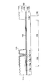
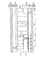
102 ブラックマトリックス
104 カラーフィルター
106 共通電極
108 液晶層
110 スペーサ
112 透過電極
113 反射電極
114 有機膜
116 パッシベーション膜
118a ソース電極
118a’ ソースライン
118b ゲート電極
118b’ ゲートライン
118c ドレーン電極
119 薄膜トランジスタ
130 下部基板
150 透過領域
160 反射領域
170 第1基板
180 第2基板
210 上部λ/4位相差フィルム
212 上部λ/2位相差フィルム
214 上部偏光板
216 Cプレート
220 下部λ/4位相差フィルム
222 下部λ/2位相差フィルム
224 下部偏光板
230 上部光学フィルムアセンブリ
240 下部光学フィルムアセンブリ
Claims (18)
- 上面及び下面を含む第1基板と、
上面及び下面を含み、前記第1基板と向かい合う第2基板と、
前記第1基板の前記上面及び前記第2基板の前記下面の間に形成され、複数個のセルギャップを有するセルと、
前記セル内に配置され、反射領域の第1セルギャップが1.8μm乃至2.2μmで、透過領域の第2セルギャップが3.6μm乃至4.0μmである垂直配向液晶層と、
前記第1基板の前記下面上に配置され、第1偏光板、前記第1基板の前記下面上に配置される第1(λ/4)位相差フィルム、及び前記第1(λ/4)位相差フィルム上に配置される第1(λ/2)位相差フィルムを含む第1光学フィルムアセンブリと、
前記第2基板の前記上面上に配置され、第2偏光板、前記第2基板の前記上面上に配置される第2(λ/4)位相差フィルム、及び前記第2(λ/4)位相差フィルム上に配置される第2(λ/2)位相差フィルムを含む第2光学フィルムアセンブリと、を含むが、
前記第2(λ/4)及び第2(λ/2)位相差フィルムのスロー軸は前記第2偏光板の吸収軸から反時計方向に15°及び75°のうちいずれの一つの角度を有し、前記第1(λ/2)位相差フィルムのスロー軸は前記第2(λ/2)位相差フィルムの前記スロー軸と80°乃至100°の角度をなし、しきい電圧は2.0V以下で、飽和電圧は4.4V以下である液晶表示装置。 - 前記第1セルギャップは2.0μmであることを特徴とする請求項1記載の液晶表示装置。
- 前記第2セルギャップは3.8μmであることを特徴とする請求項1記載の液晶表示装置。
- 前記しきい電圧は1.7Vであることを特徴とする請求項1記載の液晶表示装置。
- 前記飽和電圧は4.0Vであることを特徴とする請求項1記載の液晶表示装置。
- 前記第1偏光板の吸収軸は前記第2偏光板の吸収軸と垂直であることを特徴とする請求項1記載の液晶表示装置。
- 前記第1光学フィルムアセンブリは、前記第1(λ/2)位相差フィルム上に配置される第1偏光板を更に含むことを特徴とする請求項1記載の液晶表示装置。
- 前記第2光学フィルムアセンブリは前記第2(λ/2)位相差フィルム上に配置される第2偏光板を更に含むことを特徴とする請求項1記載の液晶表示装置。
- 前記第2(λ/4)位相差フィルムのスロー軸は前記第2偏光板の前記吸収軸を基準として反時計方向に15°傾斜することを特徴とする請求項1記載の液晶表示装置。
- 前記第2(λ/2)位相差フィルムのスロー軸は前記第2偏光板の前記吸収軸を基準として反時計方向に75°傾斜することを特徴とする請求項1記載の液晶表示装置。
- 前記第1(λ/4)位相差フィルムのスロー軸は前記第2(λ/4)位相差フィルムの前記スロー軸と80°乃至100°の範囲を有することを特徴とする請求項1記載の液晶表示装置。
- 前記第1(λ/4)位相差フィルムのスロー軸は前記第2(λ/4)位相差フィルムの前記スロー軸と垂直であることを特徴とする請求項11記載の液晶表示装置。
- 前記第1(λ/2)位相差フィルムのスロー軸は前記第2(λ/2)位相差フィルムの前記スロー軸と80°乃至100°の範囲を有することを特徴とする請求項1記載の液晶表示装置。
- 前記第1(λ/2)位相差フィルムのスロー軸は前記第2(λ/2)位相差フィルムの前記スロー軸と垂直であることを特徴とする請求項13記載の液晶表示装置。
- 前記第2光学フィルムアセンブリは、前記第2基板と前記第2(λ/4)位相差フィルムとの間に配置される補償フィルムを更に含むことを特徴とする請求項1記載の液晶表示装置。
- 前記補償フィルムはA−プレート又はC−プレートを含むことを特徴とする請求項15記載の液晶表示装置。
- 前記垂直配向液晶層のプリチルト角は45°以上であることを 特徴とする請求項1記載の液晶表示装置。
- 前記第1基板の前記下面上に配置されたバックライトアセンブリを更に含むことを特徴とする請求項1記載の液晶表示装置。
Applications Claiming Priority (2)
| Application Number | Priority Date | Filing Date | Title |
|---|---|---|---|
| KR2003-085174 | 2003-11-27 | ||
| KR1020030085174A KR20050051400A (ko) | 2003-11-27 | 2003-11-27 | 액정 표시 패널 및 이를 갖는 액정 표시 장치 |
Publications (3)
| Publication Number | Publication Date |
|---|---|
| JP2005157373A JP2005157373A (ja) | 2005-06-16 |
| JP2005157373A5 JP2005157373A5 (ja) | 2008-01-17 |
| JP4733967B2 true JP4733967B2 (ja) | 2011-07-27 |
Family
ID=34675692
Family Applications (1)
| Application Number | Title | Priority Date | Filing Date |
|---|---|---|---|
| JP2004338725A Expired - Fee Related JP4733967B2 (ja) | 2003-11-27 | 2004-11-24 | 液晶表示パネル及びこれを有する液晶表示装置。 |
Country Status (5)
| Country | Link |
|---|---|
| US (1) | US7528914B2 (ja) |
| JP (1) | JP4733967B2 (ja) |
| KR (1) | KR20050051400A (ja) |
| CN (1) | CN100465705C (ja) |
| TW (1) | TWI364589B (ja) |
Families Citing this family (9)
| Publication number | Priority date | Publication date | Assignee | Title |
|---|---|---|---|---|
| TWI294981B (ja) * | 2002-09-12 | 2008-03-21 | Au Optronics Corp | |
| JP3901172B2 (ja) * | 2004-05-28 | 2007-04-04 | セイコーエプソン株式会社 | 液晶表示装置および電子機器 |
| KR101293564B1 (ko) * | 2005-07-27 | 2013-08-06 | 삼성디스플레이 주식회사 | 액정표시장치 |
| US20080049176A1 (en) * | 2006-08-25 | 2008-02-28 | Samsung Electronics Co., Ltd. | Thin film transistor-array substrate, transflective liquid crystal display device with the same, and method for manufacturing the same |
| KR20090050795A (ko) * | 2007-11-16 | 2009-05-20 | 삼성전자주식회사 | 표시 장치와 이의 제조 방법 |
| CN102830532B (zh) * | 2012-08-20 | 2015-12-09 | 北京京东方光电科技有限公司 | 液晶显示面板、液晶显示装置及制造方法 |
| JP6439685B2 (ja) * | 2013-05-16 | 2018-12-19 | 日本ゼオン株式会社 | 静電容量式タッチパネル付き表示装置 |
| CN105223741A (zh) * | 2015-11-09 | 2016-01-06 | 信利半导体有限公司 | 一种半透半反液晶显示面板及其制造方法 |
| KR101941458B1 (ko) * | 2017-09-20 | 2019-01-23 | 엘지디스플레이 주식회사 | 접안 렌즈를 포함하는 디스플레이 장치 |
Citations (3)
| Publication number | Priority date | Publication date | Assignee | Title |
|---|---|---|---|---|
| JP2000035570A (ja) * | 1998-07-16 | 2000-02-02 | Sharp Corp | 液晶表示装置 |
| JP2003084313A (ja) * | 1998-10-15 | 2003-03-19 | Sharp Corp | 液晶表示装置 |
| JP2003207782A (ja) * | 2002-01-11 | 2003-07-25 | Stanley Electric Co Ltd | 垂直配向型液晶表示装置 |
Family Cites Families (9)
| Publication number | Priority date | Publication date | Assignee | Title |
|---|---|---|---|---|
| TW340911B (en) | 1993-05-14 | 1998-09-21 | Tektronix Inc | Low electro-optic threshold liquid crystal cell and method of fabricating the same |
| US5557434A (en) * | 1994-09-30 | 1996-09-17 | Rockwell International | Optical compensator including an o-plate for super-twist nematic liquid crystal display |
| JP3406242B2 (ja) * | 1998-10-15 | 2003-05-12 | シャープ株式会社 | 液晶表示装置 |
| JP4032568B2 (ja) * | 1999-06-30 | 2008-01-16 | カシオ計算機株式会社 | 液晶表示装置 |
| JP2003114325A (ja) * | 2001-10-03 | 2003-04-18 | Nitto Denko Corp | 積層1/4波長板、円偏光板及びこれを用いた液晶表示装置、ならびにその製造方法 |
| JP3827587B2 (ja) * | 2002-02-07 | 2006-09-27 | Nec液晶テクノロジー株式会社 | 反射型又は半透過型液晶表示装置 |
| DE60326217D1 (de) | 2002-04-02 | 2009-04-02 | Verizon Business Global Llc | Nachrichtenantwortsystem |
| KR20030079513A (ko) * | 2002-04-04 | 2003-10-10 | 삼성전자주식회사 | 보상 필름을 이용한 액정 표시 장치 |
| JP2003330022A (ja) * | 2002-05-10 | 2003-11-19 | Advanced Display Inc | 液晶表示装置 |
-
2003
- 2003-11-27 KR KR1020030085174A patent/KR20050051400A/ko not_active Application Discontinuation
-
2004
- 2004-11-24 JP JP2004338725A patent/JP4733967B2/ja not_active Expired - Fee Related
- 2004-11-24 US US10/995,474 patent/US7528914B2/en not_active Expired - Fee Related
- 2004-11-26 TW TW093136573A patent/TWI364589B/zh not_active IP Right Cessation
- 2004-11-29 CN CNB2004100471947A patent/CN100465705C/zh not_active Expired - Fee Related
Patent Citations (3)
| Publication number | Priority date | Publication date | Assignee | Title |
|---|---|---|---|---|
| JP2000035570A (ja) * | 1998-07-16 | 2000-02-02 | Sharp Corp | 液晶表示装置 |
| JP2003084313A (ja) * | 1998-10-15 | 2003-03-19 | Sharp Corp | 液晶表示装置 |
| JP2003207782A (ja) * | 2002-01-11 | 2003-07-25 | Stanley Electric Co Ltd | 垂直配向型液晶表示装置 |
Also Published As
| Publication number | Publication date |
|---|---|
| CN1629684A (zh) | 2005-06-22 |
| US7528914B2 (en) | 2009-05-05 |
| TWI364589B (en) | 2012-05-21 |
| KR20050051400A (ko) | 2005-06-01 |
| TW200530700A (en) | 2005-09-16 |
| US20050134771A1 (en) | 2005-06-23 |
| CN100465705C (zh) | 2009-03-04 |
| JP2005157373A (ja) | 2005-06-16 |
Similar Documents
| Publication | Publication Date | Title |
|---|---|---|
| US7486351B2 (en) | Liquid crystal display apparatus | |
| US6950158B2 (en) | Transflective liquid crystal display device and fabrication method thereof | |
| US8035784B2 (en) | Semi-transmissive liquid crystal display device and manufacturing method of the same | |
| JPH11242226A (ja) | 液晶表示装置 | |
| JP3538149B2 (ja) | 反射型液晶表示装置及びその製造方法 | |
| JP2828073B2 (ja) | アクティブマトリクス液晶表示装置 | |
| JP4733967B2 (ja) | 液晶表示パネル及びこれを有する液晶表示装置。 | |
| US7973889B2 (en) | Liquid crystal display having interval adjustment layer between substrates and method of producing the same | |
| JP2005157373A5 (ja) | ||
| US6882395B2 (en) | Wide viewing angle fringe field multi-domain aligned LCD with electrically conductive grids and method for fabricating | |
| JP3046730B2 (ja) | 反射拡散板および反射型液晶表示装置 | |
| US7889299B2 (en) | Liquid crystal display device and method of fabricating the same | |
| JP2002372710A (ja) | 液晶表示装置 | |
| JP2005128233A (ja) | 液晶表示装置および電子機器 | |
| JP3344557B2 (ja) | 液晶表示装置 | |
| JP2002333624A (ja) | 液晶表示装置 | |
| JP2006091930A (ja) | 液晶表示装置 | |
| JP2001147427A (ja) | 液晶表示装置 | |
| JP3795178B2 (ja) | 液晶表示装置 | |
| JPH11119215A (ja) | 反射型液晶表示素子 | |
| KR20020017048A (ko) | 반사형 및 반투과형 액정표시장치 | |
| JP2006065235A (ja) | 液晶表示装置 | |
| JP3946746B2 (ja) | 液晶表示装置 | |
| JP3946742B2 (ja) | 液晶表示装置 | |
| JP3946744B2 (ja) | 液晶表示装置 |
Legal Events
| Date | Code | Title | Description |
|---|---|---|---|
| A521 | Written amendment |
Free format text: JAPANESE INTERMEDIATE CODE: A523 Effective date: 20071126 |
|
| A621 | Written request for application examination |
Free format text: JAPANESE INTERMEDIATE CODE: A621 Effective date: 20071126 |
|
| A977 | Report on retrieval |
Free format text: JAPANESE INTERMEDIATE CODE: A971007 Effective date: 20101109 |
|
| A131 | Notification of reasons for refusal |
Free format text: JAPANESE INTERMEDIATE CODE: A131 Effective date: 20101116 |
|
| A521 | Written amendment |
Free format text: JAPANESE INTERMEDIATE CODE: A523 Effective date: 20110216 |
|
| RD02 | Notification of acceptance of power of attorney |
Free format text: JAPANESE INTERMEDIATE CODE: A7422 Effective date: 20110216 |
|
| A01 | Written decision to grant a patent or to grant a registration (utility model) |
Free format text: JAPANESE INTERMEDIATE CODE: A01 Effective date: 20110329 |
|
| A61 | First payment of annual fees (during grant procedure) |
Free format text: JAPANESE INTERMEDIATE CODE: A61 Effective date: 20110425 |
|
| FPAY | Renewal fee payment (event date is renewal date of database) |
Free format text: PAYMENT UNTIL: 20140428 Year of fee payment: 3 |
|
| R150 | Certificate of patent or registration of utility model |
Free format text: JAPANESE INTERMEDIATE CODE: R150 |
|
| FPAY | Renewal fee payment (event date is renewal date of database) |
Free format text: PAYMENT UNTIL: 20140428 Year of fee payment: 3 |
|
| S111 | Request for change of ownership or part of ownership |
Free format text: JAPANESE INTERMEDIATE CODE: R313111 |
|
| FPAY | Renewal fee payment (event date is renewal date of database) |
Free format text: PAYMENT UNTIL: 20140428 Year of fee payment: 3 |
|
| R371 | Transfer withdrawn |
Free format text: JAPANESE INTERMEDIATE CODE: R371 |
|
| S111 | Request for change of ownership or part of ownership |
Free format text: JAPANESE INTERMEDIATE CODE: R313111 |
|
| R350 | Written notification of registration of transfer |
Free format text: JAPANESE INTERMEDIATE CODE: R350 |
|
| R250 | Receipt of annual fees |
Free format text: JAPANESE INTERMEDIATE CODE: R250 |
|
| R250 | Receipt of annual fees |
Free format text: JAPANESE INTERMEDIATE CODE: R250 |
|
| R250 | Receipt of annual fees |
Free format text: JAPANESE INTERMEDIATE CODE: R250 |
|
| LAPS | Cancellation because of no payment of annual fees |