JP4733967B2 - Liquid crystal display panel and liquid crystal display device having the same. - Google Patents
Liquid crystal display panel and liquid crystal display device having the same. Download PDFInfo
- Publication number
- JP4733967B2 JP4733967B2 JP2004338725A JP2004338725A JP4733967B2 JP 4733967 B2 JP4733967 B2 JP 4733967B2 JP 2004338725 A JP2004338725 A JP 2004338725A JP 2004338725 A JP2004338725 A JP 2004338725A JP 4733967 B2 JP4733967 B2 JP 4733967B2
- Authority
- JP
- Japan
- Prior art keywords
- liquid crystal
- crystal display
- display device
- retardation film
- substrate
- Prior art date
- Legal status (The legal status is an assumption and is not a legal conclusion. Google has not performed a legal analysis and makes no representation as to the accuracy of the status listed.)
- Expired - Fee Related
Links
Images


Classifications
-
- G—PHYSICS
- G02—OPTICS
- G02F—OPTICAL DEVICES OR ARRANGEMENTS FOR THE CONTROL OF LIGHT BY MODIFICATION OF THE OPTICAL PROPERTIES OF THE MEDIA OF THE ELEMENTS INVOLVED THEREIN; NON-LINEAR OPTICS; FREQUENCY-CHANGING OF LIGHT; OPTICAL LOGIC ELEMENTS; OPTICAL ANALOGUE/DIGITAL CONVERTERS
- G02F1/00—Devices or arrangements for the control of the intensity, colour, phase, polarisation or direction of light arriving from an independent light source, e.g. switching, gating or modulating; Non-linear optics
- G02F1/01—Devices or arrangements for the control of the intensity, colour, phase, polarisation or direction of light arriving from an independent light source, e.g. switching, gating or modulating; Non-linear optics for the control of the intensity, phase, polarisation or colour
- G02F1/13—Devices or arrangements for the control of the intensity, colour, phase, polarisation or direction of light arriving from an independent light source, e.g. switching, gating or modulating; Non-linear optics for the control of the intensity, phase, polarisation or colour based on liquid crystals, e.g. single liquid crystal display cells
- G02F1/133—Constructional arrangements; Operation of liquid crystal cells; Circuit arrangements
- G02F1/1333—Constructional arrangements; Manufacturing methods
- G02F1/1335—Structural association of cells with optical devices, e.g. polarisers or reflectors
- G02F1/133553—Reflecting elements
- G02F1/133555—Transflectors
-
- G—PHYSICS
- G02—OPTICS
- G02F—OPTICAL DEVICES OR ARRANGEMENTS FOR THE CONTROL OF LIGHT BY MODIFICATION OF THE OPTICAL PROPERTIES OF THE MEDIA OF THE ELEMENTS INVOLVED THEREIN; NON-LINEAR OPTICS; FREQUENCY-CHANGING OF LIGHT; OPTICAL LOGIC ELEMENTS; OPTICAL ANALOGUE/DIGITAL CONVERTERS
- G02F1/00—Devices or arrangements for the control of the intensity, colour, phase, polarisation or direction of light arriving from an independent light source, e.g. switching, gating or modulating; Non-linear optics
- G02F1/01—Devices or arrangements for the control of the intensity, colour, phase, polarisation or direction of light arriving from an independent light source, e.g. switching, gating or modulating; Non-linear optics for the control of the intensity, phase, polarisation or colour
- G02F1/13—Devices or arrangements for the control of the intensity, colour, phase, polarisation or direction of light arriving from an independent light source, e.g. switching, gating or modulating; Non-linear optics for the control of the intensity, phase, polarisation or colour based on liquid crystals, e.g. single liquid crystal display cells
- G02F1/133—Constructional arrangements; Operation of liquid crystal cells; Circuit arrangements
- G02F1/1333—Constructional arrangements; Manufacturing methods
- G02F1/133371—Cells with varying thickness of the liquid crystal layer
-
- G—PHYSICS
- G02—OPTICS
- G02F—OPTICAL DEVICES OR ARRANGEMENTS FOR THE CONTROL OF LIGHT BY MODIFICATION OF THE OPTICAL PROPERTIES OF THE MEDIA OF THE ELEMENTS INVOLVED THEREIN; NON-LINEAR OPTICS; FREQUENCY-CHANGING OF LIGHT; OPTICAL LOGIC ELEMENTS; OPTICAL ANALOGUE/DIGITAL CONVERTERS
- G02F1/00—Devices or arrangements for the control of the intensity, colour, phase, polarisation or direction of light arriving from an independent light source, e.g. switching, gating or modulating; Non-linear optics
- G02F1/01—Devices or arrangements for the control of the intensity, colour, phase, polarisation or direction of light arriving from an independent light source, e.g. switching, gating or modulating; Non-linear optics for the control of the intensity, phase, polarisation or colour
- G02F1/13—Devices or arrangements for the control of the intensity, colour, phase, polarisation or direction of light arriving from an independent light source, e.g. switching, gating or modulating; Non-linear optics for the control of the intensity, phase, polarisation or colour based on liquid crystals, e.g. single liquid crystal display cells
- G02F1/137—Devices or arrangements for the control of the intensity, colour, phase, polarisation or direction of light arriving from an independent light source, e.g. switching, gating or modulating; Non-linear optics for the control of the intensity, phase, polarisation or colour based on liquid crystals, e.g. single liquid crystal display cells characterised by the electro-optical or magneto-optical effect, e.g. field-induced phase transition, orientation effect, guest-host interaction or dynamic scattering
- G02F1/139—Devices or arrangements for the control of the intensity, colour, phase, polarisation or direction of light arriving from an independent light source, e.g. switching, gating or modulating; Non-linear optics for the control of the intensity, phase, polarisation or colour based on liquid crystals, e.g. single liquid crystal display cells characterised by the electro-optical or magneto-optical effect, e.g. field-induced phase transition, orientation effect, guest-host interaction or dynamic scattering based on orientation effects in which the liquid crystal remains transparent
- G02F1/1393—Devices or arrangements for the control of the intensity, colour, phase, polarisation or direction of light arriving from an independent light source, e.g. switching, gating or modulating; Non-linear optics for the control of the intensity, phase, polarisation or colour based on liquid crystals, e.g. single liquid crystal display cells characterised by the electro-optical or magneto-optical effect, e.g. field-induced phase transition, orientation effect, guest-host interaction or dynamic scattering based on orientation effects in which the liquid crystal remains transparent the birefringence of the liquid crystal being electrically controlled, e.g. ECB-, DAP-, HAN-, PI-LC cells
Landscapes
- Physics & Mathematics (AREA)
- Nonlinear Science (AREA)
- Chemical & Material Sciences (AREA)
- Crystallography & Structural Chemistry (AREA)
- General Physics & Mathematics (AREA)
- Optics & Photonics (AREA)
- Mathematical Physics (AREA)
- Liquid Crystal (AREA)
- Polarising Elements (AREA)
Description
本発明は液晶表示パネル及びこれを有する液晶表示装置に関し、より詳細には垂直配向された液晶に対してセルギャップを最適化して透過率、コントラスト比及び数率が増加され設計が容易である液晶表示パネル及びこれを有して光学条件が最適化された液晶表示装置に関する。 The present invention relates to a liquid crystal display panel and a liquid crystal display device having the same, and more specifically, a liquid crystal that is easy to design by optimizing a cell gap and increasing transmittance, contrast ratio, and number ratio for vertically aligned liquid crystal. The present invention relates to a display panel and a liquid crystal display device having the display panel and having optimized optical conditions.
液晶表示装置は薄膜トランジスタが形成されたアレイ基板とカラーフィルター基板との間に注入されている異方性誘電率を有する液晶物質に電界を印加し、この電界の強度を調節して基板に透過される光の量を調節することで所望する映像信号を得る表示装置である。 In the liquid crystal display device, an electric field is applied to a liquid crystal substance having an anisotropic dielectric constant injected between an array substrate on which a thin film transistor is formed and a color filter substrate, and the intensity of the electric field is adjusted and transmitted through the substrate. It is a display device that obtains a desired video signal by adjusting the amount of light to be transmitted.
一般に、液晶は直接光を発生しないので、内部光源または外部から提供された光を用いて映像を表示する。内部光源のみを用いて映像を表示する場合、光を発生させるためのバッテリーの大きさが増加して液晶表示装置の大きさが増加するという短所がある。また、外部光のみを用いて映像を表示する場合、暗い環境では映像の輝度が減少される短所がある。しかし、外部光を反射する反射領域及び光源から発生された光が透過する透過領域を含む反射−透過型液晶表示装置を用いる場合、液晶表示装置の大きさが減少され暗い環境でも映像の輝度を保持することができる。 In general, the liquid crystal does not generate light directly, so that an image is displayed using an internal light source or light provided from the outside. When displaying an image using only an internal light source, there is a disadvantage in that the size of a liquid crystal display device increases due to an increase in the size of a battery for generating light. In addition, when displaying an image using only external light, there is a disadvantage that the luminance of the image is reduced in a dark environment. However, when a reflection-transmission type liquid crystal display device including a reflection region that reflects external light and a transmission region that transmits light generated from a light source is used, the size of the liquid crystal display device is reduced, and the luminance of an image can be reduced even in a dark environment. Can be held.
一般的に反射−透過型液晶表示装置は、液晶表示パネル及び光学フィルムを含む。前記液晶表示パネルは、第1基板、第2基板及び液晶層を含む。前記第1基板はカラーフィルター及び共通電極を含み、前記第2基板は薄膜トランジスタ、反射電極及び透明電極を含む。前記液晶層は前記第1基板と前記第2基板との間に介在される。前記光学フィルムは偏光板を含む。 In general, a reflection-transmission type liquid crystal display device includes a liquid crystal display panel and an optical film. The liquid crystal display panel includes a first substrate, a second substrate, and a liquid crystal layer. The first substrate includes a color filter and a common electrode, and the second substrate includes a thin film transistor, a reflective electrode, and a transparent electrode. The liquid crystal layer is interposed between the first substrate and the second substrate. The optical film includes a polarizing plate.
一般の反射−反射透過型液晶表示装置は、MTNモードの液晶を採用する。前記MTNモードの液晶は90°以下の角度を有するツイスト構造に配向されている。 A general reflection-reflection transmission type liquid crystal display employs MTN mode liquid crystal. The MTN mode liquid crystal is aligned in a twist structure having an angle of 90 ° or less.
しかし、液晶がツイスト構造に配向された場合、光の偏光特性によって光の損失が発生されて透過率が低下される。前記MTNモードの液晶を採用する液晶表示装置は光学条件が反射モードを中心にして設計されるので、透過モードに対してブラックを基本とする。前記透過モードに対してブラックを基本とする場合、光の偏光によりホワイト状態で一部の光のみが利用される、理論的に透過率が既存の透過型液晶表示装置に比べて50%程度に落ちる。従って、液晶表示装置の輝度及びコントラスト比が減少されるという問題点が発生する。 However, when the liquid crystal is aligned in a twisted structure, light loss is generated due to the polarization characteristics of light, and the transmittance is reduced. Since the liquid crystal display device employing the MTN mode liquid crystal is designed with the optical condition centered on the reflection mode, black is basically used for the transmission mode. When black is basically used for the transmission mode, only a part of the light is used in the white state due to the polarization of the light. Theoretically, the transmittance is about 50% compared to the existing transmission type liquid crystal display device. drop down. Accordingly, there arises a problem that the luminance and contrast ratio of the liquid crystal display device are reduced.
前記のような問題点を解決するための本発明の第1目的は、垂直配向された液晶に対してセルギャップを最適化して、コントラスト比及び数率が増加され設計が容易である液晶表示パネルを提供することにある。 SUMMARY OF THE INVENTION A first object of the present invention to solve the above-mentioned problems is to optimize a cell gap for vertically aligned liquid crystal and increase the contrast ratio and the number ratio, thereby simplifying the design. Is to provide.
本発明の第2目的は、前記液晶表示パネルを有し光学条件が最適化された液晶表示装置を提供することにある。 A second object of the present invention is to provide a liquid crystal display device having the liquid crystal display panel and having optimized optical conditions.
上記課題を解決するために、発明1は、上面及び下面を含む第1基板と、上面及び下面を含み、前記第1基板と向かい合う第2基板と、前記第1基板の前記上面及び前記第2基板の前記下面の間に形成され、複数個のセルギャップを有するセルと、前記セル内に配置され、反射領域の第1セルギャップが1.8μm乃至2.2μmで、透過領域の第2セルギャップが3.6μm乃至4.0μmである垂直配向液晶層と、前記第1基板の前記下面上に配置され、第1偏光板、前記第1基板の前記下面上に配置される第1(λ/4)位相差フィルム、及び前記第1(λ/4)位相差フィルム上に配置される第1(λ/2)位相差フィルムを含む第1光学フィルムアセンブリと、前記第2基板の前記上面上に配置され、第2偏光板、前記第2基板の前記上面上に配置される第2(λ/4)位相差フィルム、及び前記第2(λ/4)位相差フィルム上に配置される(λ/2)位相差フィルムを含む第2光学フィルムアセンブリと、を含むが、前記第2(λ/4)及び(λ/2)位相差フィルムのスロー軸は前記第2偏光板の吸収軸を基準として同じ四分面内に配置され、前記第1(λ/2)位相差フィルムのスロー軸は前記第2(λ/2)位相差フィルムの前記スロー軸と80°乃至100°の角度をなし、しきい電圧は2.0V以下で、飽和電圧は4.4V以下である液晶表示装置を提供する。垂直配向された液晶に対してセルギャップを最適化することで、コントラスト比及び数率が増加され設計が容易である液晶表示パネルを得ることができる。 In order to solve the above problems, the first aspect of the invention includes a first substrate including an upper surface and a lower surface, a second substrate including the upper surface and the lower surface and facing the first substrate, the upper surface of the first substrate, and the second substrate. A cell formed between the lower surfaces of the substrate and having a plurality of cell gaps, and a first cell gap of the reflective region disposed between the cells and having a first cell gap of 1.8 μm to 2.2 μm, and a second cell of the transmissive region A vertically aligned liquid crystal layer having a gap of 3.6 μm to 4.0 μm, a first polarizing plate disposed on the lower surface of the first substrate, and a first polarizing plate disposed on the lower surface of the first substrate (λ / 4) a phase difference film, a first optical film assembly including a first (λ / 2) phase difference film disposed on the first (λ / 4) phase difference film, and the upper surface of the second substrate Arranged on the second polarizing plate, the second substrate A second (λ / 4) retardation film disposed on the surface, and a second optical film assembly including the (λ / 2) retardation film disposed on the second (λ / 4) retardation film; The slow axes of the second (λ / 4) and (λ / 2) retardation films are arranged in the same quadrant with respect to the absorption axis of the second polarizing plate, and the first ( λ / 2) The slow axis of the retardation film forms an angle of 80 ° to 100 ° with the slow axis of the second (λ / 2) retardation film, the threshold voltage is 2.0 V or less, and the saturation voltage is A liquid crystal display device having a voltage of 4.4 V or lower is provided. By optimizing the cell gap with respect to the vertically aligned liquid crystal, a liquid crystal display panel can be obtained that has an increased contrast ratio and number ratio and is easy to design.
発明2は、発明1において、前記第1セルギャップは2.0μmであることを特徴とする。
発明3は、発明1において、前記第2セルギャップは3.8μmであることを特徴とする。 An invention 3 is the invention 1, wherein the second cell gap is 3.8 μm.
発明4は、発明1において、前記しきい電圧は1.7Vであることを特徴とする。 An
発明5は、発明1において、前記飽和電圧は4.0Vであることを特徴とする。 An invention 5 is the invention 1 characterized in that the saturation voltage is 4.0V.
発明6は、発明1において、前記第1偏光板の吸収軸は前記第2偏光板の吸収軸と垂直であることを特徴とする。 A sixth aspect of the invention is characterized in that in the first aspect, the absorption axis of the first polarizing plate is perpendicular to the absorption axis of the second polarizing plate.
発明7は、発明1において、前記第1光学フィルムアセンブリは、前記第1(λ/2)位相差フィルム上に配置される第1偏光板を更に含むことを特徴とする。 The invention 7 is the invention 1, wherein the first optical film assembly further includes a first polarizing plate disposed on the first (λ / 2) retardation film.
発明8は、発明1において、前記第2光学フィルムアセンブリは前記第2(λ/2)位相差フィルム上に配置される第2偏光板を更に含むことを特徴とする。 The invention 8 is the invention 1, wherein the second optical film assembly further includes a second polarizing plate disposed on the second (λ / 2) retardation film.
発明9は、発明1において、前記(λ/4)位相差フィルムのスロー軸は前記第2偏光板の前記吸収軸を基準として反時計方向に15°傾斜することを特徴とする。 A ninth aspect of the invention is characterized in that, in the first aspect, the slow axis of the (λ / 4) retardation film is inclined 15 ° counterclockwise with respect to the absorption axis of the second polarizing plate.
発明10は、発明1において、前記第2(λ/2)位相差フィルムのスロー軸は前記第2偏光板の前記吸収軸を基準として反時計方向に75°傾斜することを特徴とする。 Invention 10 is characterized in that, in Invention 1, the slow axis of the second (λ / 2) retardation film is inclined by 75 ° counterclockwise with respect to the absorption axis of the second polarizing plate.
発明11は、発明1において、前記第1(λ/4)位相差フィルムのスロー軸は前記第2(λ/4)位相差フィルムの前記スロー軸と80°乃至100°の範囲を有することを特徴とする。 Invention 11 is the invention 1, wherein the slow axis of the first (λ / 4) retardation film has a range of 80 ° to 100 ° with the slow axis of the second (λ / 4) retardation film. Features.
発明12は、発明13において、前記第1(λ/4)位相差フィルムのスロー軸は前記第2(λ/4)位相差フィルムの前記スロー軸と垂直であることを特徴とする。 Invention 12 is characterized in that, in Invention 13, a slow axis of the first (λ / 4) retardation film is perpendicular to the slow axis of the second (λ / 4) retardation film.
発明13は、発明1において、前記第1(λ/2)位相差フィルムのスロー軸は前記第2(λ/2)位相差フィルムの前記スロー軸と80°乃至100°の範囲を有することを特徴とする。 Invention 13 is the invention 1, wherein the slow axis of the first (λ / 2) retardation film has a range of 80 ° to 100 ° with the slow axis of the second (λ / 2) retardation film. Features.
発明14は、発明13において、前記第1(λ/2)位相差フィルムのスロー軸は前記第2(λ/2)位相差フィルムの前記スロー軸と垂直であることを特徴とする。 A fourteenth aspect of the invention is characterized in that, in the thirteenth aspect, a slow axis of the first (λ / 2) retardation film is perpendicular to the slow axis of the second (λ / 2) retardation film.
発明15は、発明1において、前記第2光学フィルムアセンブリは、前記第2基板と前記第2(λ/4)位相差フィルムとの間に配置される補償フィルムを更に含むことを特徴とする。 A fifteenth aspect of the invention is the invention according to the first aspect, wherein the second optical film assembly further includes a compensation film disposed between the second substrate and the second (λ / 4) retardation film.
発明16は、発明15において、前記補償フィルムはA−プレート又はC−プレートを含むことを特徴とする。 The invention 16 is the invention 15, wherein the compensation film includes an A-plate or a C-plate.
発明17は、発明1において、前記垂直配向液晶層のプリチルト角は45°以上であることを特徴とする。 Invention 17 is characterized in that, in Invention 1, a pretilt angle of the vertically aligned liquid crystal layer is 45 ° or more.
発明18は、発明1において、前記第1基板の前記下面上に配置されたバックライトアセンブリを更に含むことを特徴とする。 A eighteenth aspect of the invention is characterized in that, in the first aspect of the invention, the apparatus further includes a backlight assembly disposed on the lower surface of the first substrate.
発明19は、上面及び下面を含む第1基板と、上面及び下面を含み、前記第1基板と向かい合う第2基板と、前記第1基板の前記上面及び前記第2基板の前記下面間に形成され、複数個のセルギャップを有するセルと、前記セル内に配置され、反射領域の第1セルギャップが1.8μm乃至2.2μmで、透過領域の第2セルギャップが3.6μm乃至4.0μmである垂直配向液晶層と、前記第2基板の前記上面上に配置され、偏光反、前記第2基板の前記上面上に配置される(λ/4)位相差フィルム、及び前記第2基板と前記(λ/4)位相差フィルムとの間に配置される補償フィルムを含む光学フィルムアセンブリと、を含むが、しきい電圧は2.0V以下で、飽和電圧は4.4V以下である液晶表示装置を提供する。 The invention 19 is formed between a first substrate including an upper surface and a lower surface, a second substrate including the upper surface and the lower surface and facing the first substrate, the upper surface of the first substrate and the lower surface of the second substrate. A cell having a plurality of cell gaps, and a first cell gap in the reflective region is 1.8 μm to 2.2 μm and a second cell gap in the transmissive region is 3.6 μm to 4.0 μm. A vertically aligned liquid crystal layer, an anti-polarization film, a (λ / 4) retardation film disposed on the upper surface of the second substrate, and the second substrate. An optical film assembly including a compensation film disposed between the (λ / 4) retardation film, a liquid crystal display having a threshold voltage of 2.0 V or less and a saturation voltage of 4.4 V or less Providing equipment.
発明20は、上面及び下面を含む第1基板と、上面及び下面を含み、前記第1基板と向かい合う第2基板と、前記第1基板の前記上面及び前記第2基板の前記下面間に形成され、複数個のセルギャップを有するセルと、前記セル内に配置され、反射領域の第1セルギャップが1.8μm乃至2.2μmで、透過領域の第2セルギャップが3.6μm乃至4.0μmである垂直配向液晶層と、前記第1基板の前記下面上に配置され、第1偏光反、前記第1基板の前記下面上に配置される第1(λ/4)位相差フィルム、及び前記第1(λ/4)位相差フィルム上に配置される第1(λ/2)位相差フィルムを含む第1光学フィルムアセンブリと、記第2基板の前記上面上に配置され、第2偏光反、前記第2基板の前記上面上に配置される第2(λ/4)位相差フィルム、及び前記第2(λ/4)位相差フィルム上に配置される(λ/2)位相差フィルムを含む第2光学フィルムアセンブリと、を含むが、前記第1(λ/4)位相差フィルムのスロー軸は前記第2(λ/4)位相差フィルムのスロー軸と80°乃至100°の角度をなし、しきい電圧は2.0V以下で、飽和電圧は4.4V以下である液晶表示装置を提供する。 The invention 20 is formed between the first substrate including the upper surface and the lower surface, the second substrate including the upper surface and the lower surface and facing the first substrate, the upper surface of the first substrate and the lower surface of the second substrate. A cell having a plurality of cell gaps, and a first cell gap in the reflective region is 1.8 μm to 2.2 μm and a second cell gap in the transmissive region is 3.6 μm to 4.0 μm. A vertically aligned liquid crystal layer, a first polarization antireflection film disposed on the lower surface of the first substrate, a first (λ / 4) retardation film disposed on the lower surface of the first substrate, and A first optical film assembly including a first (λ / 2) retardation film disposed on the first (λ / 4) retardation film; and a second polarization antireflection film disposed on the upper surface of the second substrate. , Second (λ / 4) disposed on the upper surface of the second substrate. A retardation film, and a second optical film assembly including a (λ / 2) retardation film disposed on the second (λ / 4) retardation film, wherein the first (λ / 4) ) The slow axis of the retardation film forms an angle of 80 ° to 100 ° with the slow axis of the second (λ / 4) retardation film, the threshold voltage is 2.0V or less, and the saturation voltage is 4.4V or less. A liquid crystal display device is provided.
前記位相差フィルムはファスト軸(Fast Axis)及びスロー軸を含む。前記ファスト軸は前記位相差フィルムを進行する光の速度が速くなる方向であり、前記スロー軸は前記ファスト軸と90°の角度を有して進行する光の速度が遅くなる方向である。前記偏光板は前記吸収軸と同一の方向に振動する光を遮断する。 The retardation film includes a fast axis and a slow axis. The fast axis is a direction in which the speed of light traveling through the retardation film is increased, and the slow axis is a direction in which the speed of light traveling at an angle of 90 ° with the fast axis is decreased. The polarizing plate blocks light that vibrates in the same direction as the absorption axis.
望ましくは、前記光学フィルムアセンブリはλ/4位相差フィルム、λ/2位相差フィルム及び偏光板を含む。 Preferably, the optical film assembly includes a λ / 4 retardation film, a λ / 2 retardation film, and a polarizing plate.
偏光成分を有する光の速度が前記2つの方向で差異が発生すると、一つの偏光成分の位相が他の一つの偏光成分の位相より遅延されて前記光の偏光状態が変化される。 When a difference occurs in the speed of light having a polarization component in the two directions, the phase of one polarization component is delayed from the phase of the other polarization component, and the polarization state of the light is changed.
望ましくは、前記液晶表示装置は前記光学フィルムアセンブリと互いに向き合う追加的光学フィルムアセンブリを含む。前記追加的光学フィルムアセンブリは追加的λ/4位相差フィルム、追加的λ/2位相差フィルム及び追加的偏光板を含む。より、望ましくは、前記追加的λ/4位相差フィルムのスロー軸は前記λ/4位相差フィルムと90°の角度を有し、前記追加的λ/2位相差フィルムのスロー軸は前記λ/2位相差フィルムと90°の角度を有する。また、前記追加的偏光板の吸収軸は前記偏光板と90°の角度を有する。 Preferably, the liquid crystal display includes an additional optical film assembly facing the optical film assembly. The additional optical film assembly includes an additional λ / 4 retardation film, an additional λ / 2 retardation film, and an additional polarizing plate. More preferably, the slow axis of the additional λ / 4 retardation film has an angle of 90 ° with the λ / 4 retardation film, and the slow axis of the additional λ / 2 retardation film is the λ / Has an angle of 90 ° with the two retardation film. The absorption axis of the additional polarizing plate has an angle of 90 ° with the polarizing plate.
前記λ/4位相差フィルムは上部λ/4位相差フィルムを含み、前記λ/2位相差フィルムは上部λ/2位相差フィルムを含む。前記偏光板は上部偏光板を含む。前記追加的λ/4位相差フィルムは下部λ/4位相差フィルムを含み、前記追加的λ/2位相差フィルムは下部λ/2位相差フィルムを含む。前記追加的偏光板は下部偏光板を含む。前記λは前記位相差フィルムにより位相差が発生する光の波長を示す。 The λ / 4 retardation film includes an upper λ / 4 retardation film, and the λ / 2 retardation film includes an upper λ / 2 retardation film. The polarizing plate includes an upper polarizing plate. The additional λ / 4 retardation film includes a lower λ / 4 retardation film, and the additional λ / 2 retardation film includes a lower λ / 2 retardation film. The additional polarizing plate includes a lower polarizing plate. The λ represents the wavelength of light at which a retardation is generated by the retardation film.
従って、前記垂直配向された液晶層を含む液晶表示装置の光学フィルムの条件、前記反射領域に対応するセルギャップ及び前記透過領域に対応するセルギャップを最適化して透過率及びコントラスト比が向上される。 Accordingly, the transmittance and contrast ratio are improved by optimizing the conditions of the optical film of the liquid crystal display device including the vertically aligned liquid crystal layer, the cell gap corresponding to the reflection region, and the cell gap corresponding to the transmission region. .
また、前記λ/4位相差フィルムのスロー軸、前記λ/2位相差フィルムのスロー軸及び前記偏光板の吸収軸がそれぞれ前記追加的λ/4位相差フィルムのスロー軸、前記追加的λ/2位相差フィルムのスロー軸及び前記追加的偏光板の吸収軸と90°の角度を有して光学フィルムアセンブリの設計が容易である。 Further, the slow axis of the λ / 4 retardation film, the slow axis of the λ / 2 retardation film, and the absorption axis of the polarizing plate are the slow axis of the additional λ / 4 retardation film, and the additional λ / The 90 ° angle between the slow axis of the two retardation film and the absorption axis of the additional polarizing plate makes it easy to design the optical film assembly.
また、ホモジニアス配向された液晶を含む液晶表示装置の場合、反射領域のセルギャップが1.6μm程度に非常に小さい値であるのでパーティクルによる短絡が発生することができて数率が減少されたが、前記本発明の液晶表示装置は反射領域のセルギャップを増加させてパーティクルによる短絡が減少する。 In the case of a liquid crystal display device including homogeneously aligned liquid crystal, the cell gap of the reflection region is a very small value of about 1.6 μm, so that a short circuit due to particles can occur and the number rate is reduced. In the liquid crystal display device of the present invention, the cell gap in the reflective region is increased and the short circuit due to particles is reduced.
前記のような本発明によると、垂直配向された液晶層を含む液晶表示装置の光学フィルム条件、反射領域に対応するセルギャップ及び透過領域に対応するセルギャップを最適化して透過率及びコントラスト比が向上される。 According to the present invention as described above, the optical film condition of the liquid crystal display device including the vertically aligned liquid crystal layer, the cell gap corresponding to the reflective region, and the cell gap corresponding to the transmissive region are optimized so that the transmittance and the contrast ratio are increased. Be improved.
また、上部λ/4位相差フィルムのスロー軸、上部λ/2位相差フィルムのスロー軸及び上部偏光板の吸収軸がそれぞれ下部λ/4位相差フィルムのスロー軸、下部λ/4位相差フィルムのスロー軸及び下部偏光板の吸収軸と90°の角度を有して光学フィルムアセンブリの設計が容易である。 The slow axis of the upper λ / 4 retardation film, the slow axis of the upper λ / 2 retardation film, and the absorption axis of the upper polarizing plate are the slow axis of the lower λ / 4 retardation film and the lower λ / 4 retardation film, respectively. The angle of 90 ° with the slow axis and the absorption axis of the lower polarizer makes it easy to design an optical film assembly.
また、ホモジニアス配向された液晶を含む液晶表示装置の場合反射領域のセルギャップが1.6μm程度に非常に小さい値なのでパーティクルによる短絡が発生することができ数率が減少されるが、前記本発明の液晶表示装置は反射領域のセルギャップが1.8μm乃至2.2μmに増加されてパーティクルによる短絡が減少する。 Further, in the case of a liquid crystal display device including homogeneously aligned liquid crystal, the cell gap in the reflection region is a very small value of about 1.6 μm, so that a short circuit due to particles can occur and the number rate is reduced. In the liquid crystal display device, the cell gap of the reflection region is increased to 1.8 μm to 2.2 μm, and short circuit due to particles is reduced.
以下、図面を参照して本発明の望ましい一実施例をより詳細に説明する。 Hereinafter, a preferred embodiment of the present invention will be described in detail with reference to the drawings.
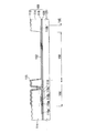
図1は本発明の第1実施例による液晶表示装置を示す分解斜視図であり、図2は本発明の第1実施例による液晶表示装置を示す断面図である。 FIG. 1 is an exploded perspective view illustrating a liquid crystal display device according to a first embodiment of the present invention, and FIG. 2 is a cross-sectional view illustrating the liquid crystal display device according to the first embodiment of the present invention.
前記液晶表示装置は液晶表示パネル200、上部光学フィルムアセンブリ230及び下部光学フィルムアセンブリ240を含む。
The liquid crystal display device includes a liquid
前記液晶表示パネル200は上部基板170、下部基板180及び液晶層108を含む。前記第1基板170は上部基板100、ブラックマトリックス102、カラーフィルター104、共通電極106及びスペーサ110を含む。前記第2基板180は下部基板120、薄膜トランジスタ119、ゲート絶縁膜126、パッシベーション膜116、有機膜114、透明電極112及び反射電極113を含む。前記第2基板180は透過領域150及び反射領域160を含む。
The liquid
前記透過領域150は下部のバックライト(図示せず)から発生された光が透過される領域であり、前記反射領域160は外部で前記液晶表示パネル200に入射される光が反射される領域である。前記透明電極112の一部は前記透過領域150内に配置され、前記薄膜トランジスタ119及び前記反射電極113は前記反射領域160内に配置される。
The
前記上部基板100及び前記下部基板120は光を通過させることができる透明な材質のガラスを使用する。前記ガラスは無アルカリ特性である。前記ガラスがアルカリ特性である場合、前記ガラスでアルカリイオンが液晶セル中に溶出されると液晶比抵抗が低下され表示特性が変化され、前記シールとガラスとの付着力を低下させ、スイッチング素子の動作に悪影響を与える。
The
前記ブラックマトリックス102は前記反射領域160に対応する前記上部基板100の一部に形成されて光を遮断する。前記ブラックマトリックス102は液晶を制御することができない領域を通過する光を遮断して画質を向上させる。前記ブラックマトリックス102は不透明の物質を蒸着しエッチングして形成される。
The
前記カラーフィルター104は前記ブラックマトリックス102が形成された前記上部基板上に形成され所定の波長分だけ光のみを選択的に透過させる。このとき、前記カラーフィルター104が前記上部基板120上に配置されることができる。
The
前記共通電極106は前記ブラックマトリックス102及び前記カラーフィルター104が形成された前記上部基板100の全面に形成される。前記共通電極106はITO、IZOまたはZOのような透明で導電性を有する物質を含む。このとき、前記共通電極106が前記下部基板120上に前記透明電極112及び前記反射電極113と並んで配置されることができる。
The
前記スペーサ110は前記ブラックマトリックス102、前記カラーフィルター104及び前記共通電極106が形成された前記上部基板100上に形成される。前記スペーサ110によって前記第1基板170と第2基板180との間の間隔が一定に保持される。望ましくは、前記スペーサ110は前記ブラックマトリックス102に対応して配置される。前記スペーサ110はカラムスペーサ(Column Spacer)、ボールスペーサ(Ball Spacer)または前記カラムスペーサと前記ボールスペーサとが混合されたスペーサを含む。このとき、前記スペーサ110は前記薄膜トランジスタ119に対応して配置されることもできる。
The
前記薄膜トランジスタ119は前記下部基板120の前記反射領域160内に形成され、ソース電極118a、ゲート電極118b、ドレイン電極118c及び半導体層パターンを含む。駆動回路(図示せず)はデータ電圧を出力してソースライン118a’を通じて前記ソース電極118aに伝達し、選択信号を出力してゲートランプ118b’を通じて前記ゲート電極118bに伝達する。
The
前記ストレージキャパシタ(図示せず)は前記下部基板120上に形成されて前記共通電極106と前記反射電極113との間または前記共通電極106と前記透過電極112との間に電位差を保持する。前記ストレージキャパシタ(図示せず)はアンドゲート方式または独立配線方式である。
The storage capacitor (not shown) is formed on the
前記ゲート絶縁膜126は前記ゲート電極118bが形成された前記下部基板120の全面に配置されて前記ゲート電極118bを前記ソース電極118a及び前記ドレイン電極118cと電気的に絶縁する。このとき、前記光の透過率を高めるために前記透過領域150内に配置された前記ゲート絶縁膜126を除去することができる。前記ゲート絶縁膜126はシリコン窒化物SiNxを含む。
The
前記パッシベーション膜116は前記薄膜トランジスタ119が形成された前記下部基板120上の全面に配置され、前記ドレイン電極118cの一部を露出する開口部を含む。このとき、前記光の透過率を高めるために前記透過領域150内に配置された前記パッシベーション膜116を取り除くことができる。前記パッシベーション膜126はシリコン窒化物を含む。
The
前記有機膜114は前記薄膜トランジスタ119及び前記パッシベーション膜126が形成された前記下部基板120上に配置されて前記薄膜トランジスタ119を前記透明電極112または前記反射電極113と絶縁する。
The
前記有機膜114により前記液晶層108の厚さが調節されて前記反射領域160及び前記透過領域150で互いに異なるセルギャップを有する液晶層108が形成される。前記透過領域150のセルギャップG2は3.6μm乃至4μmであり、前記反射領域160のセルギャップG1は1.8μm乃至2.2μmである。望ましくは、前記透過領域150のセルギャップG2は3.8μmであり、前記反射領域160のセルギャップG1は2.0μmである。また、前記透過領域150のセルギャップと前記反射領域160のセルギャップとの比は1.9:1であることが望ましい。
The thickness of the
前記液晶層108内の液晶のΔn値は0.09乃至0.11である。望ましくは、前記液晶のΔn値が0.1である。ここで、Δnは液晶の複屈折率である.液晶層に電界が加わると、液晶分子は電界方向に傾き、入射光に対する複屈折率Δnが変化する。
The Δn value of the liquid crystal in the
前記有機膜114は前記薄膜トランジスタ119、前記ソースライン118a’、前記ゲートライン118b’などが配置されて互いに異なる高さを有する前記下部基板120の表面を平坦化する役割もする。このとき、前記透過窓129内に薄い厚さの有機膜114が残留することもできる。
The
望ましくは、前記有機膜114の上部表面は凹部及び凸部を有する。前記凹部及び凸部は前記反射電極113の反射効率を増加させる。このとき、前記有機膜114の上部表面は凹部及び凸部がない平坦な面であることもできる。
Preferably, the upper surface of the
前記透明電極112は前記パッシベーション膜116上の前記透過領域150、前記有機膜114上の前記反射領域160の一部及び前記ドレイン電極118cの一部を露出する開口部の内面上に形成されて前記ドレイン電極118cと電気的に連結される。前記透明電極112は前記共通電極106との間に印加された電圧により前記液晶層108内の液晶を制御して光の透過を調節する。前記透明電極112は透明で導電性を有するインジウムすず酸化物質ITO、インジウム亜鉛酸化物質IZO、亜鉛酸化物質ZOなどを含む。このとき、前記透明電極112の一部が前記反射領域160内の前記有機膜114上に配置されることもできる。
The
前記反射電極113は前記反射領域160内の前記有機膜114上に配置されて外部光を反射させる。望ましくは、前記反射電極113は前記有機膜114の上部表面上に形成された凹部及び凸部の形状に沿って配置されて外部光を一定の方向に反射させる。前記反射電極113は導電性物質を含んで前記透明電極112を通じて前記ドレイン電極118cと電気的に連結される。
The
前記駆動回路(図示せず)は前記薄膜トランジスタ119を通じて前記透明電極112及び前記反射電極113にデータ電圧を提供して前記共通電極106と前記透明電極112との間及び前記共通電極106と前記反射電極113との間に電界を形成する。望ましくは、前記電極106、112、113の間のしきい電圧は2V以下であり、前記電極106、112、114の間の飽和電圧は4.4Vである。さらに望ましくは、前記しきい電圧は1.7Vであり、前記飽和電圧は4Vである。前記しきい電圧は液晶が駆動されるための最小限の電圧を示す。前記飽和電圧以上の電圧が加えられると前記液晶駆動の効果は次のようである。
The driving circuit (not shown) provides a data voltage to the
前記液晶を配向するために、前記第1基板170及び前記第2基板180の表面に配向膜(図示せず)を配置し、前記配向膜(図示せず)の表面を一定の方向にラビングする。前記ラビングによって前記液晶が一定の方向に配向される。前記上部基板上に配置された配向膜(図示せず)のラビング方向は前記下部基板上に配置された配向膜(図示せず)のラビング方向と互いに反対の方向である。
In order to align the liquid crystal, an alignment layer (not shown) is disposed on the surfaces of the
前記液晶層108は前記第1基板170と前記第2基板180との間に配置されてシール(図示せず)により密封される。前記液晶層108内の液晶は前記配向膜(図示せず)により前記第1基板170または前記第2基板180の面に垂直する方向に配向される。望ましくは、前記液晶は所定の角度でプリーティルト(Pre‐tilted)されてある。
The
前記上部光学フィルムアセンブリ230は上部λ/4位相差フィルム210、上部λ/2位相差フィルム212及び上部偏光板214を含み、前記下部光学フィルムアセンブリ240は下部λ/4位相差フィルム220、下部λ/2位相差フィルム222及び下部偏光板224を含む。
The upper
前記上部光学フィルムアセンブリ230と前記下部光学フィルムアセンブリ240は互いに向き合う位置に配置され、前記上部偏光板214と前記下部偏光板224の吸収軸は互いに90°の角度を有する。前記上部偏光板214と前記下部偏光板224の吸収軸が互いに90°の角度を有し前記液晶が垂直配向される場合、ノーマリブラックモード(Normally Black Mode)を具現して画質が向上される。即ち、前記電極106、112、113に電圧が印加されない場合、前記ノーマリブラックモードでは光が遮断されて光漏れ現象が減少して画質が向上される。
The upper
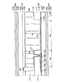
図3は本発明の第1実施例による液晶表示装置の上部光学フィルムアセンブリを示す分解斜視図である。 FIG. 3 is an exploded perspective view showing an upper optical film assembly of the liquid crystal display device according to the first embodiment of the present invention.
図3に示すように、前記上部λ/4位相差フィルム210は前記上部基板100の上部表面上に配置され、前記上部λ/4位相差フィルム210のスロー軸(slow axis)は前記上部偏光板214の吸収軸から反時計方向に15°の角度を有する。前記上部λ/2位相差フィルム212は前記上部λ/4位相差フィルム210上に配置され、前記上部λ/2位相差フィルム212のスロー軸は前記上部偏光板214の吸収軸から反時計方向に75°の角度を有する。前記位相差フィルムはファスト軸(Fast Axis)及びスロー軸を含む。前記ファスト軸は前記位相差フィルムを進行する光の速度が速くなる方向であり、前記スロー軸は前記ファスト軸と90°の角度を有して進行する光の速度が遅くなる方向である。前記偏光板は前記吸収軸と同一の方向に振動する光を遮断する。偏光成分を有する光の速度が前記2つの方向で差異が発生すると、一つの偏光成分の位相が他の一つの偏光成分の位相より遅延されて前記光の偏光状態が変化される。
As shown in FIG. 3, the upper λ / 4
前記上部λ/4位相差フィルム210のΔnd(リタデーション)は130nm乃至150nmであり、前記上部λ/2位相差フィルム212のΔndは265nm乃至285nmである。望ましくは、前記上部λ/4位相差フィルム210のΔndは140nmであり、前記上部λ/2位相差フィルム212のΔndは275nmである。さらに望ましくは、前記Δndは550nmの波長を有する光を基準にして決定される。前記Δndは550nmの波長を有する光を基準とする。
Δnd (retardation) of the upper λ / 4
図4は本発明の第1実施例による液晶表示装置の下部光学フィルムアセンブリを示す分解斜視図である。 FIG. 4 is an exploded perspective view showing a lower optical film assembly of the liquid crystal display device according to the first embodiment of the present invention.
図4に示すように前記下部λ/4位相差フィルム220は前記上部基板120の下部表面上に配置され、前記下部λ/4位相差フィルム220と前記上部λ/4位相差フィルム210のスロー軸は互いに80°乃至100°の角度を有する。前記下部λ/2位相差フィルム222は前記下部λ/4位相差フィルム220上に配置され、前記下部λ/4位相差フィルム222と前記上部λ/2位相差フィルム212のスロー軸は互いに80°乃至100°の角度を有する。
As shown in FIG. 4, the lower λ / 4
望ましくは、前記下部λ/4位相差フィルム220と前記上部λ/4位相差フィルム210のスロー軸は互いに90°の角度を有し、前記下部λ/2位相差フィルム222と前記上部λ/2位相差フィルム212のスロー軸は互いに90°の角度を有する。
Preferably, the slow axes of the lower λ / 4
前記下部λ/4のΔndは130nm乃至150nmであり。前記下部λ/2のΔndは265nm乃至285nmである。望ましくは、前記下部λ/4のΔndは140nmであり、前記下部λ/2のΔndは275nmである。さらに望ましくは。前記Δndは550nmの波長を有する光を基準にして決定される。 Δnd of the lower λ / 4 is 130 nm to 150 nm. Δnd of the lower λ / 2 is 265 nm to 285 nm. Preferably, Δnd of the lower λ / 4 is 140 nm, and Δnd of the lower λ / 2 is 275 nm. More desirable. The Δnd is determined with reference to light having a wavelength of 550 nm.
図5乃至図11は本発明の第1実施例による液晶表示装置の製造方法を示す断面図である。 5 to 11 are cross-sectional views illustrating a method of manufacturing a liquid crystal display according to the first embodiment of the present invention.
図5に示すように、まず、前記下部基板120に前記バックライトアセンブリ(図示せず)から発生された前記光を透過させる透過領域150及び前記外部光を反射させる前記反射領域160を定義する。
As shown in FIG. 5, first, a
図6に示すように、続いて前記下部基板120上に導電性物質を蒸着する。続いて、前記導電性物質の一部を除去して前記ゲート電極118b及び前記ゲートライン118b’を形成する。以後、前記ゲート電極118b及び前記ゲートライン118b’が形成された下部基板120の全面に前記ゲート絶縁膜126を蒸着する。前記ゲート絶縁膜126は透明な絶縁物質を含む。望ましくは、前記ゲート絶縁膜126はシリコン窒化膜SiNxを含む。
Next, as shown in FIG. 6, a conductive material is deposited on the
続いて、アモルファスシリコン及びN+アモルファスシリコンを蒸着しエッチングして前記ゲート電極118bに対応する前記ゲート絶縁膜126上に前記半導体層を形成する。続いて、前記半導体層が形成された前記ゲート絶縁膜126上に導電性物質を蒸着する。以後、前記導電性物質の一部をエッチングして前記ソース電極118a、前記ソースライン118a’及び前記ドレイン電極118cを形成する。従って、前記ソース電極118a、前記ゲート電極118b、前記ドレイン電極118c及び前記半導体層を含む前記薄膜トランジスタ119が形成される。
Subsequently, amorphous silicon and N + amorphous silicon are deposited and etched to form the semiconductor layer on the
続いて、前記薄膜トランジスタ119が形成された前記下部基板120上に透明な絶縁物質を蒸着してパッシベーション膜を形成する。望ましくは、前記透明な絶縁物質はシリコン窒化物質を含む。
Subsequently, a transparent insulating material is deposited on the
図7に示すように、続いて前記パッシベーション膜116上に有機物質を塗布して有機膜を形成する。望ましくは、前記有機物質をフォトレジスト成分を含む。
As shown in FIG. 7, an organic material is subsequently formed on the
以後、前記有機膜を露光及び現象して前記ドレイン電極118cの一部及び前記透過領域150を露出し上部表面に前記凹部と前記凸部を有する有機膜114を形成する。前記露光及び現象工程は一つのマスクを用いた一度の工程または複数のマスクを有する複数回の工程を含む。
Thereafter, the organic film is exposed to light, and a part of the
前記有機膜114の厚さは前記透過領域150及び前記反射領域160のセルギャップを調節する。前記透過領域150のセルギャップG2は3.6μm乃至4μmであり、前記反射領域160のセルギャップG1は1.8μm乃至2.2μmである。望ましくは、前記透過領域150のセルギャップG2と前記反射領域160のセルギャップG1との比は1.9:1である。さらに望ましくは、前記液晶層内の液晶のΔn値は0.1009であり、前記透過領域150に対応するセルギャップG2は3.8であり、前記反射領域160に対応するセルギャップG1は2μmである。
The thickness of the
続いて、前記有機膜114及び前記パッシベーション膜116上に透明で導電性を有する物質を蒸着する。続いて、前記透明で導電性物質の一部をエッチングして透明電極112を形成する。
Subsequently, a transparent and conductive material is deposited on the
以後、前記有機膜114及び前記透明電極112上に反射率が高い導電体を蒸着する。望ましくは、前記反射率が高い導電体はアルミニウム及びネオジムNdを含む。続いて、前記反射率が高い導電体の一部をエッチングして前記反射領域160内に前記反射電極113を形成する。
Thereafter, a highly reflective conductor is deposited on the
このとき、前記反射電極113は多層構造を有することができる。前記反射電極が多層構造を有する場合、望ましくは、前記反射電極113はモリブデンMo−ダングステンW合金層及び前記モリブデンMo−ダングステンW合金層に形成されたアルミニウムAl−ネオジムNd合金層を含む。
At this time, the
続いて、前記反射電極113が形成された下部基板180上に配向膜(図示せず)を形成する。前記配向膜(図示せず)は所定の方向にラビングされている。
Subsequently, an alignment film (not shown) is formed on the
従って、前記下部基板120、前記スイッチング素子119、前記ソースライン118a’、前記ゲートライン118b’、前記有機膜114、前記透明電極112、前記反射電極113及び前記配向膜(図示せず)を含む前記第2基板180が形成される。
Accordingly, the
図8に示すように、続いて前記上部基板100上に不透明の物質を蒸着する。続いて、前記不透明な物質の一部を除去して前記ブラックマトリックス102を形成する。
As shown in FIG. 8, an opaque material is subsequently deposited on the
以後、前記ブラックマトリックス102が形成された前記上部基板100上にカラーフィルター104を形成する。前記カラーフィルター104は特定の光のみを選択的に透過させる。このとき、前記カラーフィルター104が前記上部基板100ではなく前記下部基板120上に形成されることもできる。前記カラーフィルター104が前記下部基板120上に形成される場合前記カラーフィルターは前記有機膜214を形成する前に形成することが望ましい。
Thereafter, a
続いて、前記カラーフィルター104及び前記ブラックマトリックス102が形成された上部基板100上に透明で導電性物質を蒸着して共通電極106を形成する。
Subsequently, a
続いて、前記共通電極106上に有機物を塗布する。望ましくは、前記有機物はフォトレジスト成分を含む。以後、前記有機物を露光及び現象して前記ブラックマトリックス102に対応する前記共通電極106の一部上にスペーサ110を形成する。このとき、前記共通電極106上にスペーサ110を形成しないで前記ボールスペーサを配置することもできる。
Subsequently, an organic material is applied on the
以後、前記スペーサ110が形成された前記上部基板170上に前記下部基板120上の前記配向膜(図示せず)の配向方向と反対方向にラビングされた配向膜(図示せず)を形成する。
Thereafter, an alignment film (not shown) rubbed in a direction opposite to the alignment direction of the alignment film (not shown) on the
従って、前記上部基板100、前記ブラックマトリックス102、前記カラーフィルター104、前記共通電極106、前記スペーサ110及び前記配向膜(図示せず)を含む第1基板170が形成される。
Accordingly, the
図9に示すように、続いて前記第1基板170と前記第2基板180を対向して結合する。続いて、前記第1基板170及び前記第2基板180との間に液晶層108を注入して後シール(図示せず)により密封される。このとき、前記シール(図示せず)が形成された前記第1基板170または前記第2基板180上に液晶を滴下した後前記第1基板170及び第2基板180を対向して結合し前記液晶層108を形成することもできる。
As shown in FIG. 9, the
図10に示すように、以後前記上部基板100の上部表面上に前記上部λ/4位相差フィルム210を形成する。
As shown in FIG. 10, the upper λ / 4
続いて、前記上部λ/4位相差フィルム210上に前記上部λ/2位相差フィルム212を形成する。このとき、前記上部λ/2位相差フィルム212のスロー軸は前記上部λ/4位相差フィルム210のスロー軸から反時計方向に60°の角度を有する。
Subsequently, the upper λ / 2
以後、前記上部λ/2位相差フィルム212上に上部偏光板214を形成する。このとき、上部偏光板214の吸収軸は前記上部λ/4位相差フィルム210のスロー軸から時計方向に15°の角度を有する。
Thereafter, an upper
従って、前記上部λ/4位相差フィルム210、前記上部λ/2位相差フィルム212及び前記上部偏光板214を含む前記上部光学フィルムアセンブリが前記第1基板230の上部表面上に形成される。
Accordingly, the upper optical film assembly including the upper λ / 4
図11に示すように、以後前記下部基板120の上部表面上に前記下部λ/4位相差フィルム220を形成する。このとき、前記下部λ/4位相差フィルム220のスロー軸は前記上部λ/4位相差フィルム210と90°の角度を有する。
Referring to FIG. 11, the lower λ / 4
続いて、前記下部λ/4位相差フィルム220上に前記下部λ/2位相差フィルム222を形成する。このとき、前記下部λ/2位相差フィルム222のスロー軸は前記下部λ/4のスロー軸と90°の角度を有する。
Subsequently, the lower λ / 2
以後、前記下部λ/2位相差フィルム222上に前記下部偏光板224を形成する。このとき、前記下部偏光板224の吸収軸は前記上部偏光板214と90°の角度を有する。
Thereafter, the lower
従って、前記下部λ/4位相差フィルム220、前記下部λ/2位相差フィルム222及び前記下部偏光板224を含む前記下部光学フィルムアセンブリが前記第2基板180の下部表面上に形成される。
Accordingly, the lower optical film assembly including the lower λ / 4
従って、前記所定のセルギャップの比を有する複数のセルギャップを有し垂直方向に配向された前記液晶層108、前記上部光学フィルムアセンブリ230及び前記上部光学フィルムアセンブリ230と向き合う前記下部光学フィルムアセンブリ240を用いて輝度及びコントラスト比が向上される。
Accordingly, the
図12は本発明の第2実施例による液晶表示装置を示す分解斜視図であり、図13は本発明の第2実施例による液晶表示装置を示す断面図であり、図13は本発明の第2実施例による液晶表示装置を示す断面図である。本実施例で視野角を増加させる補償フィルムを除いては残りの構成要素は実施例1と同一であるので重複された部分に対しては詳細な説明を省略する。 FIG. 12 is an exploded perspective view showing a liquid crystal display device according to a second embodiment of the present invention, FIG. 13 is a cross-sectional view showing a liquid crystal display device according to the second embodiment of the present invention, and FIG. It is sectional drawing which shows the liquid crystal display device by 2 Example. Except for the compensation film that increases the viewing angle in the present embodiment, the remaining components are the same as those in the first embodiment, and therefore, detailed description of the overlapped portions is omitted.
液晶表示装置は液晶の異方性に起因して光が透過する方向によって画質に差異が発生して一定の視野角の範囲内のみで良質の映像を得ることができる。一般に、視野角はコントラスト比が10:1以上である映像を得ることができる角度を示す。コントラスト比は画面で明るいところと暗いところとの明るさの差異を示す。前記コントラスト比は液晶表示装置がより暗い状態を具現することができるか、より均一な輝度を有する場合増加する。前記本発明の前記光学フィルムアセンブリ230、240はノーマリブラックモードで動作するので暗い状態を示すことが可能である。
The liquid crystal display device can obtain a good quality image only within a certain viewing angle range due to a difference in image quality depending on the direction of light transmission due to the anisotropy of the liquid crystal. Generally, the viewing angle indicates an angle at which an image with a contrast ratio of 10: 1 or more can be obtained. The contrast ratio indicates the difference in brightness between a bright place and a dark place on the screen. The contrast ratio increases when the liquid crystal display device can realize a darker state or has a more uniform luminance. Since the
前記液晶表示装置は輝度を均一にするために、前記視野角を増加させる補償フィルムを含む。前記補償フィルムはA−プレートまたはC−プレート216を含む。前記A−プレート及び前記C−プレート216は一軸性フィルムである。
The liquid crystal display device includes a compensation film for increasing the viewing angle in order to make the luminance uniform. The compensation film includes an A-plate or a C-
前記A−プレートのx方向の屈折率nxとy方向の屈折率nyは同一であり、z方向の屈折率nzは前記x方向の屈折率nxまたは前記y方向の屈折率nyより大きい。前記C−プレート216のx方向の屈折率nxとy方向の屈折率nyは同一であり、z方向の屈折率nzは前記x方向の屈折率nxまたは前記y方向の屈折率nyより小さい。
The refractive index nx in the x direction and the refractive index ny in the y direction of the A-plate are the same, and the refractive index nz in the z direction is greater than the refractive index nx in the x direction or the refractive index ny in the y direction. The refractive index nx in the x direction and the refractive index ny in the y direction of the C-
望ましくは、前記補償フィルムは前記C−プレート216である。前記C―プレート216は前記上部基板100と前記λ/4位相差フィルム210との間に配置される。前記C−プレート216により前記液晶表示装置の輝度が均一になって、視野角特性が向上される。従って、正面ではない方向でも良質の映像を得ることができる。
Preferably, the compensation film is the C-
前記C−プレート216を含む液晶表示装置を製造するためには、まず、前記液晶表示パネル200を形成する。
In order to manufacture a liquid crystal display device including the C-
続いて、前記液晶表示パネル200の上部表面上の所定厚さにコレステリック液晶をコーティングし配向させた後非偏光紫外線を照射して前記コレステリック液晶の配向状態を固定させて一軸性フィルムを形成する。望ましくは、前記一軸性フィルムは前記C−フィルム216である。
Subsequently, the cholesteric liquid crystal is coated and oriented to a predetermined thickness on the upper surface of the liquid
続いて、前記C−プレート216上に前記上部光学フィルムアセンブリ230を形成する。最後に、前記液晶表示パネル200の下部表面上に前記下部光学フィルムアセンブリ240を形成する。
Subsequently, the upper
従って、前記液晶表示装置が前記C−プレート216を含んで輝度が均一になり視野角が増加される。
実験例1
本実験例での数値解釈はドイツのオトロニック−メルチャス社(Autronic−MELCHERSGmbH)のダイモスシミュレーション(Dimos Simulation)プログラムを利用し、本実験例の液晶表示装置は本発明の第1実施例による液晶表示装置である。本実施例において、実施例1と同一の構成要素の重複された部分に対しては詳細な説明を省略する。
Accordingly, the liquid crystal display device includes the C-
Experimental example 1
The numerical interpretation in this experimental example uses the Dimos Simulation program of Autotronic-MELCHERSGmbH of Germany, and the liquid crystal display device of this experimental example is a liquid crystal display according to the first embodiment of the present invention. Device. In the present embodiment, detailed description of the same components as those in the first embodiment is omitted.
図14は反射領域に対応するセルギャップの変化による反射率を示すグラフであり、図15は反射領域に対応するセルギャップの変化によるコントラスト比を示すグラフである。図14の横軸は前記電極106、112、113の間に加えられた電圧を示し、縦軸は液晶表示装置の反射率を示す。図15の横軸は前記反射セルギャップを示し、縦軸は液晶表示装置のコントラスト比を示す。
FIG. 14 is a graph showing the reflectivity due to the change in the cell gap corresponding to the reflection region, and FIG. 15 is a graph showing the contrast ratio due to the change in the cell gap corresponding to the reflection region. The horizontal axis in FIG. 14 indicates the voltage applied between the
前記多様な反射セルギャップを有する液晶表示装置は本発明の第1実施例による前記上部光学フィルムアセンブリ230と、前記下部光学フィルムアセンブリ240と、前記垂直配向された液晶層108を有する液晶表示パネル200を含む。
The liquid crystal display device having various reflective cell gaps includes a liquid
図14に示すように、反射セルギャップ1.8μm以上の場合高い反射率を示した。前記電圧が3.8V以下の場合、反射セルギャップが増加するほど反射率が増加した。前記電圧が3.82V以上の場合、前記電圧及び前記反射セルギャップによって反射率が互いに異なる値を有する。前記電圧が4Vであり、前記反射セルギャップが2μmである場合、反射率が最も大きかった。 As shown in FIG. 14, when the reflective cell gap was 1.8 μm or more, a high reflectance was shown. When the voltage was 3.8 V or less, the reflectance increased as the reflective cell gap increased. When the voltage is equal to or higher than 3.82 V, the reflectivity varies depending on the voltage and the reflective cell gap. When the voltage was 4V and the reflection cell gap was 2 μm, the reflectivity was the largest.
図15に示すように、前記液晶表示装置のコントラスト比は前記反射セルギャップの変化に対して複数のピーク(Peak)を示す。前記反射セルギャップが1.65μmの場合、コントラスト比が603で最も大きい。前記反射セルギャップが2μmの場合、コントラスト比が527である。 As shown in FIG. 15, the contrast ratio of the liquid crystal display device shows a plurality of peaks with respect to the change of the reflection cell gap. When the reflection cell gap is 1.65 μm, the contrast ratio is 603, which is the largest. When the reflection cell gap is 2 μm, the contrast ratio is 527.
図16は透過領域に対応するセルギャップの変化による透過率を示すグラフであり、図17は透過領域に対応するセルギャップの変化によるコントラスト比を示すグラフである。図16の横軸は前記電極106、112、113の間に加えられた電圧を示し、縦軸は液晶表示装置の透過率を示す。図17の横軸は前記透過セルギャップを示し、縦軸は液晶表示装置のコントラスト比を示す。
FIG. 16 is a graph showing the transmittance due to the change in the cell gap corresponding to the transmissive region, and FIG. 17 is a graph showing the contrast ratio due to the change in the cell gap corresponding to the transmissive region. The horizontal axis in FIG. 16 indicates the voltage applied between the
前記多様な透過セルギャップを有する液晶表示装置は本発明の第1実施例による前記液晶表示パネル、前記上部光学フィルムアセンブリ230と、前記下部光学フィルムアセンブリ240を含み、垂直配向された液晶層108の反射セルギャップは2μmであった。
The liquid crystal display device having various transmissive cell gaps includes the liquid crystal display panel, the upper
図16に示すように、透過セルギャップが3.6μm以上の場合高い透過率を示す。前記電圧が3.7V以下の場合、反射セルギャップが増加するほど透過率が増加する。前記電圧が3.7V以上の場合、前記電圧及び前記反射セルギャップによって透過率が互いに異なる値を有する。前記電圧が4Vであり、前記反射セルギャップが3.8μmの場合、透過率が最も大きい。 As shown in FIG. 16, high transmittance is exhibited when the transmission cell gap is 3.6 μm or more. When the voltage is 3.7 V or less, the transmittance increases as the reflection cell gap increases. When the voltage is 3.7 V or higher, the transmittances have different values depending on the voltage and the reflection cell gap. When the voltage is 4V and the reflection cell gap is 3.8 μm, the transmittance is the largest.
図17に示すように、前記液晶表示装置のコントラスト比は前記透過セルギャップが3.8μmのとき10720で最も大きい。 As shown in FIG. 17, the contrast ratio of the liquid crystal display device is the largest at 10720 when the transmission cell gap is 3.8 μm.
以下、水平方向でホモジニアス配向された液晶を含む液晶表示装置と本発明の第1実施例による液晶表示装置とを比較した。 Hereinafter, the liquid crystal display device including the liquid crystal homogeneously aligned in the horizontal direction and the liquid crystal display device according to the first embodiment of the present invention were compared.
前記本発明の第1実施例による液晶表示装置は垂直配向モードの液晶を含み、前記透過領域に対応するセルギャップ及び前記反射領域に対応するセルギャップがそれぞれ3,8μm及び2μmである。しかし、前記垂直配向でホモジニアス配向された液晶を含む液晶表示装置は前記透過領域に対応するセルギャップ及び前記反射領域に対応するセルギャップがそれぞれ3.3μm及び1.6μmである。 The liquid crystal display according to the first embodiment of the present invention includes a vertical alignment mode liquid crystal, and the cell gap corresponding to the transmission region and the cell gap corresponding to the reflection region are 3, 8 μm and 2 μm, respectively. However, in the liquid crystal display device including liquid crystal that is homogeneously aligned in the vertical alignment, the cell gap corresponding to the transmission region and the cell gap corresponding to the reflection region are 3.3 μm and 1.6 μm, respectively.
表1は本発明の第1実施例による液晶表示装置及び水平方向にホモジニアス配向された液晶を含む液晶表示装置の反射モードでの光特性を示す。前記水平方向にホモジニアス配向された液晶を含む液晶表示装置は反射領域に対応するセルギャップ1.6μmである。 Table 1 shows optical characteristics in the reflection mode of the liquid crystal display device according to the first embodiment of the present invention and the liquid crystal display device including the liquid crystal homogeneously aligned in the horizontal direction. The liquid crystal display device including liquid crystals that are homogeneously aligned in the horizontal direction has a cell gap of 1.6 μm corresponding to the reflective region.

表1に示すように、‘白色(%)’は前記液晶表示装置が白色を表示する場合の反射率を示し、‘黒色(%)’は前記液晶表示装置が黒色を表示する場合の反射率を示す。前記コントラスト比は前記‘白色(%)’を前記‘黒色(%)’で割り算した値である。前記‘白色(%)’が増加し前記‘黒色(%)’が減少するほど前記コントラスト比が増加する。前記本発明の第1実施例による液晶表示装置のコントラスト比は48.3であり、前記従来の液晶表示装置のコントラスト比は33.7である。従って、前記本発明の第1実施例による液晶表示装置のコントラスト比が前記従来の液晶表示装置のコントラスト比に比べて43.3%増加した。
As shown in Table 1, “white (%)” indicates the reflectance when the liquid crystal display device displays white, and “black (%)” indicates the reflectance when the liquid crystal display device displays black. Indicates. The contrast ratio is a value obtained by dividing the “white (%)” by the “black (%)”. The contrast ratio increases as the “white (%)” increases and the “black (%)” decreases. The contrast ratio of the liquid crystal display device according to the first embodiment of the present invention is 48.3, and the contrast ratio of the conventional liquid crystal display device is 33.7. Accordingly, the contrast ratio of the liquid crystal display device according to the first embodiment of the present invention is increased by 43.3% compared to the contrast ratio of the conventional liquid crystal display device.
図18は反射モード及び透過モードで表示される白色の色座標を示すグラフである。 FIG. 18 is a graph showing white color coordinates displayed in the reflection mode and the transmission mode.
図18に示すように、前記‘白色の色座標’は前記液晶表示装置により表示された白色の位置を示す、白色の光を色温度に従って分類する場合、太陽光D65は6500Kに該当する。前記6500Kの色温度に当る色座標値はxが0.31でyは0.392である。前記本発明の第1実施例による液晶表示装置において白色の色座標R1のx及びyが0.3161と0.3502であり、前記従来の液晶表示装置での白色の色座標R2のx及びyが0.3286と0.3625である。従って、前記本発明の液晶表示装置が表示する白色が前記太陽光とさらに類似する。 As shown in FIG. 18, the “white color coordinate” indicates a white position displayed by the liquid crystal display device. When white light is classified according to color temperature, sunlight D65 corresponds to 6500K. The color coordinate value corresponding to the color temperature of 6500K is 0.31 for x and 0.392 for y. In the liquid crystal display device according to the first embodiment of the present invention, x and y of the white color coordinate R1 are 0.3161 and 0.3502, and x and y of the white color coordinate R2 in the conventional liquid crystal display device. Are 0.3286 and 0.3625. Therefore, the white color displayed by the liquid crystal display device of the present invention is more similar to the sunlight.
表2は本発明の第1実施例による液晶表示装置及び水平方向にホモジニアス配向された液晶を含む液晶表示装置の透過モードでの光特定を示す。前記水平方向にホモジニアス配向された液晶を含む液晶表示装置は透過領域に対応するセルギャップが3.3μmである。 Table 2 shows the light specification in the transmission mode of the liquid crystal display device according to the first embodiment of the present invention and the liquid crystal display device including the liquid crystal homogeneously aligned in the horizontal direction. The liquid crystal display device including liquid crystals that are homogeneously aligned in the horizontal direction has a cell gap of 3.3 μm corresponding to the transmission region.
表2に示すように‘白色(Cd/m2)’は前記液晶表示装置が白色を表示する場合の透過光の強度を示し、‘黒色(Cd/m2)’は前記液晶表示装置が黒色を表示する場合の透過光の強度率を示す。前記コントラスト比は前記‘白色(Cd/m2)’を前記‘黒色(Cd/m2)’で割り算した値である。前記本発明の第1実施例による液晶表示装置のコントラスト比は482であり、前記従来の液晶表示装置のコントラスト比は198である。従って、前記本発明の第1実施例による液晶表示装置のコントラスト比が前記従来の液晶表示装置のコントラスト比に比べて143%増加した。
As shown in Table 2, “white (Cd / m 2)” indicates the intensity of transmitted light when the liquid crystal display device displays white, and “black (Cd / m 2)” indicates that the liquid crystal display device displays black. In this case, the intensity ratio of transmitted light is shown. The contrast ratio is a value obtained by dividing the “white (Cd / m 2)” by the “black (Cd / m 2)”. The contrast ratio of the liquid crystal display according to the first embodiment of the present invention is 482, and the contrast ratio of the conventional liquid crystal display is 198. Accordingly, the contrast ratio of the liquid crystal display device according to the first embodiment of the present invention is increased by 143% compared to the contrast ratio of the conventional liquid crystal display device.
図18に示すように、前記本発明の第1実施例による液晶表示装置で白色の色座標T1のx及びyが0.3113と0.3331であり、前記従来の液晶表示装置で白色の色座標T2のx及びyが0.3112と0.3289である。前記白色の色座標の場合前記本発明の第1実施例による液晶表示装置と前記従来の液晶表示装置との間で大きい差異がない。 As shown in FIG. 18, in the liquid crystal display device according to the first embodiment of the present invention, the x and y of the white color coordinate T1 are 0.3113 and 0.3331, and the white color in the conventional liquid crystal display device. The x and y of the coordinate T2 are 0.3112 and 0.3289. In the case of the white color coordinates, there is no significant difference between the liquid crystal display device according to the first embodiment of the present invention and the conventional liquid crystal display device.
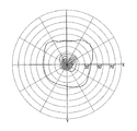
図19は数値解釈によって得られた視野角による透過コントラスト比を示すグラフであり、図20は本発明の第1実施例による液晶表示装置の視野角によるコントラスト比を示すグラフである。図19及び図20の同心円の中心からの距離である半径軸(Radial Axis)は前記液晶表示装置の視野角を示し、前記同心円の中心からの方向である角度軸は前記液晶表示パネルを基準にした前記視野角の方向を示す。それぞれの同心円は10間隔を有するコントラスト比を示す。図19及び図20に示すように、コントラスト比が10:1である閉曲線は約80°の視野角である。 FIG. 19 is a graph showing the transmission contrast ratio depending on the viewing angle obtained by numerical interpretation, and FIG. 20 is a graph showing the contrast ratio depending on the viewing angle of the liquid crystal display device according to the first embodiment of the present invention. 19 and 20, a radial axis that is a distance from the center of the concentric circle indicates a viewing angle of the liquid crystal display device, and an angle axis that is a direction from the center of the concentric circle is based on the liquid crystal display panel. The direction of the viewing angle is shown. Each concentric circle represents a contrast ratio having 10 intervals. As shown in FIGS. 19 and 20, a closed curve with a contrast ratio of 10: 1 has a viewing angle of about 80 °.
以上、本発明の実施例によって詳細に説明したが、本発明はこれに限定されず、本発明が属する技術分野において通常の知識を有する者であれば、本発明の思想と精神を離れることなく、本発明を修正または変更できる。 As described above, the embodiments of the present invention have been described in detail. However, the present invention is not limited thereto, and those who have ordinary knowledge in the technical field to which the present invention belongs can be used without departing from the spirit and spirit of the present invention. The present invention can be modified or changed.
100 上部基板
102 ブラックマトリックス
104 カラーフィルター
106 共通電極
108 液晶層
110 スペーサ
112 透過電極
113 反射電極
114 有機膜
116 パッシベーション膜
118a ソース電極
118a’ ソースライン
118b ゲート電極
118b’ ゲートライン
118c ドレーン電極
119 薄膜トランジスタ
130 下部基板
150 透過領域
160 反射領域
170 第1基板
180 第2基板
210 上部λ/4位相差フィルム
212 上部λ/2位相差フィルム
214 上部偏光板
216 Cプレート
220 下部λ/4位相差フィルム
222 下部λ/2位相差フィルム
224 下部偏光板
230 上部光学フィルムアセンブリ
240 下部光学フィルムアセンブリ
100
Claims (18)
上面及び下面を含み、前記第1基板と向かい合う第2基板と、
前記第1基板の前記上面及び前記第2基板の前記下面の間に形成され、複数個のセルギャップを有するセルと、
前記セル内に配置され、反射領域の第1セルギャップが1.8μm乃至2.2μmで、透過領域の第2セルギャップが3.6μm乃至4.0μmである垂直配向液晶層と、
前記第1基板の前記下面上に配置され、第1偏光板、前記第1基板の前記下面上に配置される第1(λ/4)位相差フィルム、及び前記第1(λ/4)位相差フィルム上に配置される第1(λ/2)位相差フィルムを含む第1光学フィルムアセンブリと、
前記第2基板の前記上面上に配置され、第2偏光板、前記第2基板の前記上面上に配置される第2(λ/4)位相差フィルム、及び前記第2(λ/4)位相差フィルム上に配置される第2(λ/2)位相差フィルムを含む第2光学フィルムアセンブリと、を含むが、
前記第2(λ/4)及び第2(λ/2)位相差フィルムのスロー軸は前記第2偏光板の吸収軸から反時計方向に15°及び75°のうちいずれの一つの角度を有し、前記第1(λ/2)位相差フィルムのスロー軸は前記第2(λ/2)位相差フィルムの前記スロー軸と80°乃至100°の角度をなし、しきい電圧は2.0V以下で、飽和電圧は4.4V以下である液晶表示装置。 A first substrate including an upper surface and a lower surface;
A second substrate including an upper surface and a lower surface and facing the first substrate;
A cell formed between the upper surface of the first substrate and the lower surface of the second substrate and having a plurality of cell gaps;
A vertically aligned liquid crystal layer disposed in the cell and having a first cell gap of a reflective region of 1.8 μm to 2.2 μm and a second cell gap of a transmissive region of 3.6 μm to 4.0 μm;
A first polarizing plate disposed on the lower surface of the first substrate, a first (λ / 4) retardation film disposed on the lower surface of the first substrate, and the first (λ / 4) position A first optical film assembly including a first (λ / 2) retardation film disposed on the retardation film;
A second polarizing plate disposed on the upper surface of the second substrate; a second (λ / 4) retardation film disposed on the upper surface of the second substrate; and the second (λ / 4) position. A second optical film assembly including a second (λ / 2) retardation film disposed on the retardation film,
The slow axes of the second (λ / 4) and second (λ / 2) retardation films have an angle of either 15 ° or 75 ° counterclockwise from the absorption axis of the second polarizing plate. and the slow axis of the 1 (λ / 2) retardation film without the angle of the slow axis 80 ° to 100 ° of the first 2 (λ / 2) retardation film, the threshold voltage is 2.0V A liquid crystal display device having a saturation voltage of 4.4 V or less below.
The liquid crystal display device according to claim 1, further comprising a backlight assembly disposed on the lower surface of the first substrate.
Applications Claiming Priority (2)
| Application Number | Priority Date | Filing Date | Title |
|---|---|---|---|
| KR2003-085174 | 2003-11-27 | ||
| KR1020030085174A KR20050051400A (en) | 2003-11-27 | 2003-11-27 | Liquid crystal display panel and liquid crystal display apparatus having the same |
Publications (3)
| Publication Number | Publication Date |
|---|---|
| JP2005157373A JP2005157373A (en) | 2005-06-16 |
| JP2005157373A5 JP2005157373A5 (en) | 2008-01-17 |
| JP4733967B2 true JP4733967B2 (en) | 2011-07-27 |
Family
ID=34675692
Family Applications (1)
| Application Number | Title | Priority Date | Filing Date |
|---|---|---|---|
| JP2004338725A Expired - Fee Related JP4733967B2 (en) | 2003-11-27 | 2004-11-24 | Liquid crystal display panel and liquid crystal display device having the same. |
Country Status (5)
| Country | Link |
|---|---|
| US (1) | US7528914B2 (en) |
| JP (1) | JP4733967B2 (en) |
| KR (1) | KR20050051400A (en) |
| CN (1) | CN100465705C (en) |
| TW (1) | TWI364589B (en) |
Families Citing this family (9)
| Publication number | Priority date | Publication date | Assignee | Title |
|---|---|---|---|---|
| TWI294981B (en) * | 2002-09-12 | 2008-03-21 | Au Optronics Corp | |
| JP3901172B2 (en) * | 2004-05-28 | 2007-04-04 | セイコーエプソン株式会社 | Liquid crystal display device and electronic device |
| KR101293564B1 (en) * | 2005-07-27 | 2013-08-06 | 삼성디스플레이 주식회사 | Liquid crystal display device |
| US20080049176A1 (en) * | 2006-08-25 | 2008-02-28 | Samsung Electronics Co., Ltd. | Thin film transistor-array substrate, transflective liquid crystal display device with the same, and method for manufacturing the same |
| KR20090050795A (en) * | 2007-11-16 | 2009-05-20 | 삼성전자주식회사 | Display device and method thereof |
| CN102830532B (en) * | 2012-08-20 | 2015-12-09 | 北京京东方光电科技有限公司 | Display panels, liquid crystal indicator and manufacture method |
| WO2014185000A1 (en) * | 2013-05-16 | 2014-11-20 | 日本ゼオン株式会社 | Display device with capacitive touch panel |
| CN105223741A (en) * | 2015-11-09 | 2016-01-06 | 信利半导体有限公司 | A kind of semitransparent semi-inverse liquid crystal display panel and manufacture method thereof |
| KR101941458B1 (en) * | 2017-09-20 | 2019-01-23 | 엘지디스플레이 주식회사 | Display device having an eyepiece |
Citations (3)
| Publication number | Priority date | Publication date | Assignee | Title |
|---|---|---|---|---|
| JP2000035570A (en) * | 1998-07-16 | 2000-02-02 | Sharp Corp | Liquid crystal display device |
| JP2003084313A (en) * | 1998-10-15 | 2003-03-19 | Sharp Corp | Liquid crystal display device |
| JP2003207782A (en) * | 2002-01-11 | 2003-07-25 | Stanley Electric Co Ltd | Vertically aligned liquid crystal display device |
Family Cites Families (9)
| Publication number | Priority date | Publication date | Assignee | Title |
|---|---|---|---|---|
| TW340911B (en) | 1993-05-14 | 1998-09-21 | Tektronix Inc | Low electro-optic threshold liquid crystal cell and method of fabricating the same |
| US5557434A (en) * | 1994-09-30 | 1996-09-17 | Rockwell International | Optical compensator including an o-plate for super-twist nematic liquid crystal display |
| JP3406242B2 (en) | 1998-10-15 | 2003-05-12 | シャープ株式会社 | Liquid crystal display |
| JP4032568B2 (en) * | 1999-06-30 | 2008-01-16 | カシオ計算機株式会社 | Liquid crystal display |
| JP2003114325A (en) * | 2001-10-03 | 2003-04-18 | Nitto Denko Corp | Laminated quarter-wave plate, circularly polarizing plate and liquid crystal display device using the same, and method for manufacturing the same |
| JP3827587B2 (en) * | 2002-02-07 | 2006-09-27 | Nec液晶テクノロジー株式会社 | Reflective or transflective liquid crystal display device |
| US7382868B2 (en) | 2002-04-02 | 2008-06-03 | Verizon Business Global Llc | Telephony services system with instant communications enhancements |
| KR20030079513A (en) * | 2002-04-04 | 2003-10-10 | 삼성전자주식회사 | Liquid crystal display using compensation film |
| JP2003330022A (en) * | 2002-05-10 | 2003-11-19 | Advanced Display Inc | Liquid crystal display |
-
2003
- 2003-11-27 KR KR1020030085174A patent/KR20050051400A/en not_active Application Discontinuation
-
2004
- 2004-11-24 JP JP2004338725A patent/JP4733967B2/en not_active Expired - Fee Related
- 2004-11-24 US US10/995,474 patent/US7528914B2/en not_active Expired - Fee Related
- 2004-11-26 TW TW093136573A patent/TWI364589B/en not_active IP Right Cessation
- 2004-11-29 CN CNB2004100471947A patent/CN100465705C/en not_active Expired - Fee Related
Patent Citations (3)
| Publication number | Priority date | Publication date | Assignee | Title |
|---|---|---|---|---|
| JP2000035570A (en) * | 1998-07-16 | 2000-02-02 | Sharp Corp | Liquid crystal display device |
| JP2003084313A (en) * | 1998-10-15 | 2003-03-19 | Sharp Corp | Liquid crystal display device |
| JP2003207782A (en) * | 2002-01-11 | 2003-07-25 | Stanley Electric Co Ltd | Vertically aligned liquid crystal display device |
Also Published As
| Publication number | Publication date |
|---|---|
| US7528914B2 (en) | 2009-05-05 |
| US20050134771A1 (en) | 2005-06-23 |
| CN100465705C (en) | 2009-03-04 |
| JP2005157373A (en) | 2005-06-16 |
| KR20050051400A (en) | 2005-06-01 |
| TWI364589B (en) | 2012-05-21 |
| CN1629684A (en) | 2005-06-22 |
| TW200530700A (en) | 2005-09-16 |
Similar Documents
| Publication | Publication Date | Title |
|---|---|---|
| US7486351B2 (en) | Liquid crystal display apparatus | |
| US6950158B2 (en) | Transflective liquid crystal display device and fabrication method thereof | |
| US8035784B2 (en) | Semi-transmissive liquid crystal display device and manufacturing method of the same | |
| JPH11242226A (en) | Liquid crystal display device | |
| JP3538149B2 (en) | Reflection type liquid crystal display device and manufacturing method thereof | |
| JP2828073B2 (en) | Active matrix liquid crystal display | |
| JP4733967B2 (en) | Liquid crystal display panel and liquid crystal display device having the same. | |
| US7973889B2 (en) | Liquid crystal display having interval adjustment layer between substrates and method of producing the same | |
| JP2005157373A5 (en) | ||
| US6882395B2 (en) | Wide viewing angle fringe field multi-domain aligned LCD with electrically conductive grids and method for fabricating | |
| JP3046730B2 (en) | Reflective diffuser and reflective liquid crystal display | |
| US7889299B2 (en) | Liquid crystal display device and method of fabricating the same | |
| JP2002372710A (en) | Liquid crystal display device | |
| JP2005128233A (en) | Liquid crystal display device and electronic appliance | |
| JP3344557B2 (en) | Liquid crystal display | |
| JP2002333624A (en) | Liquid crystal display device | |
| JP2006091930A (en) | Liquid crystal display | |
| JP2001147427A (en) | Liquid crystal display device | |
| JP3795178B2 (en) | Liquid crystal display | |
| JPH11119215A (en) | Reflection type liquid crystal display device | |
| KR20020017048A (en) | Reflective and Transflective Liquid Crystal Display Device | |
| JP2006065235A (en) | Liquid crystal display device | |
| JP3946746B2 (en) | Liquid crystal display | |
| JP3946742B2 (en) | Liquid crystal display | |
| JP3946744B2 (en) | Liquid crystal display |
Legal Events
| Date | Code | Title | Description |
|---|---|---|---|
| A521 | Written amendment |
Free format text: JAPANESE INTERMEDIATE CODE: A523 Effective date: 20071126 |
|
| A621 | Written request for application examination |
Free format text: JAPANESE INTERMEDIATE CODE: A621 Effective date: 20071126 |
|
| A977 | Report on retrieval |
Free format text: JAPANESE INTERMEDIATE CODE: A971007 Effective date: 20101109 |
|
| A131 | Notification of reasons for refusal |
Free format text: JAPANESE INTERMEDIATE CODE: A131 Effective date: 20101116 |
|
| A521 | Written amendment |
Free format text: JAPANESE INTERMEDIATE CODE: A523 Effective date: 20110216 |
|
| RD02 | Notification of acceptance of power of attorney |
Free format text: JAPANESE INTERMEDIATE CODE: A7422 Effective date: 20110216 |
|
| A01 | Written decision to grant a patent or to grant a registration (utility model) |
Free format text: JAPANESE INTERMEDIATE CODE: A01 Effective date: 20110329 |
|
| A61 | First payment of annual fees (during grant procedure) |
Free format text: JAPANESE INTERMEDIATE CODE: A61 Effective date: 20110425 |
|
| FPAY | Renewal fee payment (event date is renewal date of database) |
Free format text: PAYMENT UNTIL: 20140428 Year of fee payment: 3 |
|
| R150 | Certificate of patent or registration of utility model |
Free format text: JAPANESE INTERMEDIATE CODE: R150 |
|
| FPAY | Renewal fee payment (event date is renewal date of database) |
Free format text: PAYMENT UNTIL: 20140428 Year of fee payment: 3 |
|
| S111 | Request for change of ownership or part of ownership |
Free format text: JAPANESE INTERMEDIATE CODE: R313111 |
|
| FPAY | Renewal fee payment (event date is renewal date of database) |
Free format text: PAYMENT UNTIL: 20140428 Year of fee payment: 3 |
|
| R371 | Transfer withdrawn |
Free format text: JAPANESE INTERMEDIATE CODE: R371 |
|
| S111 | Request for change of ownership or part of ownership |
Free format text: JAPANESE INTERMEDIATE CODE: R313111 |
|
| R350 | Written notification of registration of transfer |
Free format text: JAPANESE INTERMEDIATE CODE: R350 |
|
| R250 | Receipt of annual fees |
Free format text: JAPANESE INTERMEDIATE CODE: R250 |
|
| R250 | Receipt of annual fees |
Free format text: JAPANESE INTERMEDIATE CODE: R250 |
|
| R250 | Receipt of annual fees |
Free format text: JAPANESE INTERMEDIATE CODE: R250 |
|
| LAPS | Cancellation because of no payment of annual fees |