JP4733752B2 - Solderable elastic electrical contact terminals - Google Patents
Solderable elastic electrical contact terminals Download PDFInfo
- Publication number
- JP4733752B2 JP4733752B2 JP2009045556A JP2009045556A JP4733752B2 JP 4733752 B2 JP4733752 B2 JP 4733752B2 JP 2009045556 A JP2009045556 A JP 2009045556A JP 2009045556 A JP2009045556 A JP 2009045556A JP 4733752 B2 JP4733752 B2 JP 4733752B2
- Authority
- JP
- Japan
- Prior art keywords
- contact terminal
- insulating
- electrical contact
- heat
- coating layer
- Prior art date
- Legal status (The legal status is an assumption and is not a legal conclusion. Google has not performed a legal analysis and makes no representation as to the accuracy of the status listed.)
- Active
Links
- 229910052751 metal Inorganic materials 0.000 claims abstract description 57
- 239000002184 metal Substances 0.000 claims abstract description 57
- 239000010410 layer Substances 0.000 claims abstract description 55
- 229920006254 polymer film Polymers 0.000 claims abstract description 54
- 239000011247 coating layer Substances 0.000 claims abstract description 52
- 238000010073 coating (rubber) Methods 0.000 claims abstract description 48
- 229920001821 foam rubber Polymers 0.000 claims abstract 6
- 229910000679 solder Inorganic materials 0.000 claims description 23
- 239000006071 cream Substances 0.000 claims description 22
- 239000000463 material Substances 0.000 claims description 12
- 239000007788 liquid Substances 0.000 claims description 10
- 238000003825 pressing Methods 0.000 claims description 8
- 229920001721 polyimide Polymers 0.000 claims description 7
- 239000002390 adhesive tape Substances 0.000 claims description 6
- 239000004642 Polyimide Substances 0.000 claims description 5
- ATJFFYVFTNAWJD-UHFFFAOYSA-N Tin Chemical compound [Sn] ATJFFYVFTNAWJD-UHFFFAOYSA-N 0.000 claims description 4
- 238000005187 foaming Methods 0.000 claims description 4
- 229910052718 tin Inorganic materials 0.000 claims description 4
- 238000005530 etching Methods 0.000 claims description 3
- 239000000843 powder Substances 0.000 claims description 3
- 229920001971 elastomer Polymers 0.000 claims description 2
- PCHJSUWPFVWCPO-UHFFFAOYSA-N gold Chemical compound [Au] PCHJSUWPFVWCPO-UHFFFAOYSA-N 0.000 claims description 2
- 229910052737 gold Inorganic materials 0.000 claims description 2
- 239000010931 gold Substances 0.000 claims description 2
- 229910052709 silver Inorganic materials 0.000 claims description 2
- 239000004332 silver Substances 0.000 claims description 2
- 238000005476 soldering Methods 0.000 description 37
- 229920002379 silicone rubber Polymers 0.000 description 21
- 239000000853 adhesive Substances 0.000 description 16
- 230000001070 adhesive effect Effects 0.000 description 16
- 238000004519 manufacturing process Methods 0.000 description 11
- 239000004944 Liquid Silicone Rubber Substances 0.000 description 9
- 238000000034 method Methods 0.000 description 7
- 230000008569 process Effects 0.000 description 5
- RYGMFSIKBFXOCR-UHFFFAOYSA-N Copper Chemical compound [Cu] RYGMFSIKBFXOCR-UHFFFAOYSA-N 0.000 description 4
- 230000006835 compression Effects 0.000 description 4
- 238000007906 compression Methods 0.000 description 4
- 238000012669 compression test Methods 0.000 description 4
- 229910052802 copper Inorganic materials 0.000 description 4
- 239000010949 copper Substances 0.000 description 4
- 238000007747 plating Methods 0.000 description 3
- 238000011084 recovery Methods 0.000 description 3
- 239000004945 silicone rubber Substances 0.000 description 3
- 239000011135 tin Substances 0.000 description 3
- IJGRMHOSHXDMSA-UHFFFAOYSA-N Atomic nitrogen Chemical compound N#N IJGRMHOSHXDMSA-UHFFFAOYSA-N 0.000 description 2
- 230000008901 benefit Effects 0.000 description 2
- DMFGNRRURHSENX-UHFFFAOYSA-N beryllium copper Chemical compound [Be].[Cu] DMFGNRRURHSENX-UHFFFAOYSA-N 0.000 description 2
- 239000007769 metal material Substances 0.000 description 2
- 238000012986 modification Methods 0.000 description 2
- 230000004048 modification Effects 0.000 description 2
- 230000002787 reinforcement Effects 0.000 description 2
- 230000003014 reinforcing effect Effects 0.000 description 2
- 230000000630 rising effect Effects 0.000 description 2
- 239000007787 solid Substances 0.000 description 2
- 238000004544 sputter deposition Methods 0.000 description 2
- 229920001187 thermosetting polymer Polymers 0.000 description 2
- BQCADISMDOOEFD-UHFFFAOYSA-N Silver Chemical compound [Ag] BQCADISMDOOEFD-UHFFFAOYSA-N 0.000 description 1
- 238000005452 bending Methods 0.000 description 1
- 230000015572 biosynthetic process Effects 0.000 description 1
- 238000005266 casting Methods 0.000 description 1
- 238000007796 conventional method Methods 0.000 description 1
- 238000003851 corona treatment Methods 0.000 description 1
- 238000005536 corrosion prevention Methods 0.000 description 1
- 230000002950 deficient Effects 0.000 description 1
- 230000000994 depressogenic effect Effects 0.000 description 1
- 238000009713 electroplating Methods 0.000 description 1
- 239000003623 enhancer Substances 0.000 description 1
- 230000004907 flux Effects 0.000 description 1
- 238000010438 heat treatment Methods 0.000 description 1
- 238000009413 insulation Methods 0.000 description 1
- 239000006247 magnetic powder Substances 0.000 description 1
- 238000002156 mixing Methods 0.000 description 1
- 239000000203 mixture Substances 0.000 description 1
- 229910052757 nitrogen Inorganic materials 0.000 description 1
- 239000003960 organic solvent Substances 0.000 description 1
- 238000004806 packaging method and process Methods 0.000 description 1
- 230000000149 penetrating effect Effects 0.000 description 1
- 230000002093 peripheral effect Effects 0.000 description 1
- 230000000704 physical effect Effects 0.000 description 1
- 230000009467 reduction Effects 0.000 description 1
- 230000001105 regulatory effect Effects 0.000 description 1
- 239000004447 silicone coating Substances 0.000 description 1
- 238000004381 surface treatment Methods 0.000 description 1
- 229910000859 α-Fe Inorganic materials 0.000 description 1
Images


Classifications
-
- H—ELECTRICITY
- H05—ELECTRIC TECHNIQUES NOT OTHERWISE PROVIDED FOR
- H05K—PRINTED CIRCUITS; CASINGS OR CONSTRUCTIONAL DETAILS OF ELECTRIC APPARATUS; MANUFACTURE OF ASSEMBLAGES OF ELECTRICAL COMPONENTS
- H05K3/00—Apparatus or processes for manufacturing printed circuits
- H05K3/40—Forming printed elements for providing electric connections to or between printed circuits
- H05K3/4007—Surface contacts, e.g. bumps
- H05K3/4015—Surface contacts, e.g. bumps using auxiliary conductive elements, e.g. pieces of metal foil, metallic spheres
-
- H—ELECTRICITY
- H01—ELECTRIC ELEMENTS
- H01R—ELECTRICALLY-CONDUCTIVE CONNECTIONS; STRUCTURAL ASSOCIATIONS OF A PLURALITY OF MUTUALLY-INSULATED ELECTRICAL CONNECTING ELEMENTS; COUPLING DEVICES; CURRENT COLLECTORS
- H01R12/00—Structural associations of a plurality of mutually-insulated electrical connecting elements, specially adapted for printed circuits, e.g. printed circuit boards [PCB], flat or ribbon cables, or like generally planar structures, e.g. terminal strips, terminal blocks; Coupling devices specially adapted for printed circuits, flat or ribbon cables, or like generally planar structures; Terminals specially adapted for contact with, or insertion into, printed circuits, flat or ribbon cables, or like generally planar structures
- H01R12/50—Fixed connections
- H01R12/51—Fixed connections for rigid printed circuits or like structures
- H01R12/55—Fixed connections for rigid printed circuits or like structures characterised by the terminals
- H01R12/57—Fixed connections for rigid printed circuits or like structures characterised by the terminals surface mounting terminals
-
- H—ELECTRICITY
- H01—ELECTRIC ELEMENTS
- H01R—ELECTRICALLY-CONDUCTIVE CONNECTIONS; STRUCTURAL ASSOCIATIONS OF A PLURALITY OF MUTUALLY-INSULATED ELECTRICAL CONNECTING ELEMENTS; COUPLING DEVICES; CURRENT COLLECTORS
- H01R12/00—Structural associations of a plurality of mutually-insulated electrical connecting elements, specially adapted for printed circuits, e.g. printed circuit boards [PCB], flat or ribbon cables, or like generally planar structures, e.g. terminal strips, terminal blocks; Coupling devices specially adapted for printed circuits, flat or ribbon cables, or like generally planar structures; Terminals specially adapted for contact with, or insertion into, printed circuits, flat or ribbon cables, or like generally planar structures
- H01R12/70—Coupling devices
- H01R12/71—Coupling devices for rigid printing circuits or like structures
- H01R12/712—Coupling devices for rigid printing circuits or like structures co-operating with the surface of the printed circuit or with a coupling device exclusively provided on the surface of the printed circuit
- H01R12/714—Coupling devices for rigid printing circuits or like structures co-operating with the surface of the printed circuit or with a coupling device exclusively provided on the surface of the printed circuit with contacts abutting directly the printed circuit; Button contacts therefore provided on the printed circuit
-
- H—ELECTRICITY
- H01—ELECTRIC ELEMENTS
- H01R—ELECTRICALLY-CONDUCTIVE CONNECTIONS; STRUCTURAL ASSOCIATIONS OF A PLURALITY OF MUTUALLY-INSULATED ELECTRICAL CONNECTING ELEMENTS; COUPLING DEVICES; CURRENT COLLECTORS
- H01R13/00—Details of coupling devices of the kinds covered by groups H01R12/70 or H01R24/00 - H01R33/00
- H01R13/02—Contact members
- H01R13/22—Contacts for co-operating by abutting
- H01R13/24—Contacts for co-operating by abutting resilient; resiliently-mounted
-
- H—ELECTRICITY
- H05—ELECTRIC TECHNIQUES NOT OTHERWISE PROVIDED FOR
- H05K—PRINTED CIRCUITS; CASINGS OR CONSTRUCTIONAL DETAILS OF ELECTRIC APPARATUS; MANUFACTURE OF ASSEMBLAGES OF ELECTRICAL COMPONENTS
- H05K2201/00—Indexing scheme relating to printed circuits covered by H05K1/00
- H05K2201/01—Dielectrics
- H05K2201/0104—Properties and characteristics in general
- H05K2201/0133—Elastomeric or compliant polymer
-
- H—ELECTRICITY
- H05—ELECTRIC TECHNIQUES NOT OTHERWISE PROVIDED FOR
- H05K—PRINTED CIRCUITS; CASINGS OR CONSTRUCTIONAL DETAILS OF ELECTRIC APPARATUS; MANUFACTURE OF ASSEMBLAGES OF ELECTRICAL COMPONENTS
- H05K2201/00—Indexing scheme relating to printed circuits covered by H05K1/00
- H05K2201/01—Dielectrics
- H05K2201/0137—Materials
- H05K2201/0154—Polyimide
-
- H—ELECTRICITY
- H05—ELECTRIC TECHNIQUES NOT OTHERWISE PROVIDED FOR
- H05K—PRINTED CIRCUITS; CASINGS OR CONSTRUCTIONAL DETAILS OF ELECTRIC APPARATUS; MANUFACTURE OF ASSEMBLAGES OF ELECTRICAL COMPONENTS
- H05K2201/00—Indexing scheme relating to printed circuits covered by H05K1/00
- H05K2201/08—Magnetic details
- H05K2201/083—Magnetic materials
-
- H—ELECTRICITY
- H05—ELECTRIC TECHNIQUES NOT OTHERWISE PROVIDED FOR
- H05K—PRINTED CIRCUITS; CASINGS OR CONSTRUCTIONAL DETAILS OF ELECTRIC APPARATUS; MANUFACTURE OF ASSEMBLAGES OF ELECTRICAL COMPONENTS
- H05K3/00—Apparatus or processes for manufacturing printed circuits
- H05K3/22—Secondary treatment of printed circuits
- H05K3/222—Completing of printed circuits by adding non-printed jumper connections
-
- H—ELECTRICITY
- H05—ELECTRIC TECHNIQUES NOT OTHERWISE PROVIDED FOR
- H05K—PRINTED CIRCUITS; CASINGS OR CONSTRUCTIONAL DETAILS OF ELECTRIC APPARATUS; MANUFACTURE OF ASSEMBLAGES OF ELECTRICAL COMPONENTS
- H05K3/00—Apparatus or processes for manufacturing printed circuits
- H05K3/30—Assembling printed circuits with electric components, e.g. with resistor
- H05K3/32—Assembling printed circuits with electric components, e.g. with resistor electrically connecting electric components or wires to printed circuits
- H05K3/325—Assembling printed circuits with electric components, e.g. with resistor electrically connecting electric components or wires to printed circuits by abutting or pinching, i.e. without alloying process; mechanical auxiliary parts therefor
-
- H—ELECTRICITY
- H05—ELECTRIC TECHNIQUES NOT OTHERWISE PROVIDED FOR
- H05K—PRINTED CIRCUITS; CASINGS OR CONSTRUCTIONAL DETAILS OF ELECTRIC APPARATUS; MANUFACTURE OF ASSEMBLAGES OF ELECTRICAL COMPONENTS
- H05K3/00—Apparatus or processes for manufacturing printed circuits
- H05K3/30—Assembling printed circuits with electric components, e.g. with resistor
- H05K3/32—Assembling printed circuits with electric components, e.g. with resistor electrically connecting electric components or wires to printed circuits
- H05K3/34—Assembling printed circuits with electric components, e.g. with resistor electrically connecting electric components or wires to printed circuits by soldering
- H05K3/341—Surface mounted components
Abstract
Description
本発明は、電気接触端子に関し、特に、対象物と印刷回路基板を電気的及び機構的に連結しながら半田付け可能な弾性電気接触端子に関する。特に、本発明は、表面実装によるリフロー半田付け(Reflow soldering)可能な弾性電気接触端子に関する。 The present invention relates to an electrical contact terminal, and more particularly to an elastic electrical contact terminal that can be soldered while electrically and mechanically connecting an object and a printed circuit board. In particular, the present invention relates to an elastic electrical contact terminal capable of reflow soldering by surface mounting.
一般に、半田付け(soldering)可能な弾性電気接触端子は、電気伝導度が良く、弾性回復力が優れ、半田付け温度に耐えられるべきである。 In general, a solderable elastic electrical contact terminal should have good electrical conductivity, good resiliency, and withstand the soldering temperature.
従来では、リフロー半田付け可能な電気接触端子として金属材質を主に使用した。特に、金属材質の中で、ベリリウム銅(Beryllium Copper)は、弾性回復力がよく、電気伝導度が優れ、電気接触端子として広く使用された。例えば、0.3mm以下の厚さと一定幅を有するベリリウム銅シートをプレス金型により一定形状に打ち抜いた後、熱処理工程を経て弾性回復力を向上させた電気接触端子を作製した。 Conventionally, metal materials are mainly used as electrical contact terminals that can be reflow soldered. In particular, among metal materials, beryllium copper has good elastic recovery and excellent electrical conductivity, and has been widely used as an electrical contact terminal. For example, after a beryllium copper sheet having a thickness of 0.3 mm or less and a certain width was punched out into a certain shape by a press die, an electrical contact terminal with improved elastic recovery force was produced through a heat treatment step.
このように、金属シートからなる電気接触端子は、金属の特性上または構造上、一定高さ以下では、優れた弾性を提供できないという欠点がある。即ち、弾性を有するためには、一定形状に折曲げるべきであり、この折曲げ高さにより電気接触端子の高さのほとんどが決定されるため、一定高さ以下では、弾性を提供するのが不可能である。また、1つのプレス金型では、1形状の製品のみを作製できるため、他の形状の製品を製作しようとすると、更に高価のプレス金型が必要となる問題がある。更に、金属シートからなり、重さが軽くて表面実装(Surface Mounting)時に供給される風により動くことがあり、不良になりやすいという欠点がある。 As described above, the electrical contact terminal made of a metal sheet has a drawback that it cannot provide excellent elasticity at a certain height or less due to the characteristics or structure of the metal. That is, in order to have elasticity, it should be bent into a certain shape, and most of the height of the electric contact terminal is determined by this bending height, so that it provides elasticity below a certain height. Impossible. In addition, since one press mold can produce only one shape product, there is a problem that an expensive press die is required to produce another shape product. Furthermore, it is made of a metal sheet, has a disadvantage that it is light in weight and may move due to the wind supplied during surface mounting, which tends to be defective.
更に他の従来技術としては、米国ゴア(Gore)社の特許文献1がある。本特許によると、電気伝導性ガスケット材料と半田付け可能な保持層を固定する手段、即ち、別途の接着剤が必要であるという欠点がある。更に、接触手段により電気抵抗が大きくなるという欠点がある。 As another prior art, there is Patent Document 1 of Gore, USA. According to this patent, there is a disadvantage that a means for fixing the electrically conductive gasket material and the solderable holding layer, ie a separate adhesive, is required. Furthermore, there is a drawback that the electrical resistance is increased by the contact means.
更に他の従来技術としては、米国ゴア社の特許文献2がある。本特許によると、圧縮穴が形成された電気伝導性ガスケット材料の圧縮穴と、電気伝導性ガスケット材料の底面にクリンプ(crimp)工程を有する電気伝導性保持層が形成され、EMIガスケットアセンブリを生産する時、生産性が劣るという欠点がある。即ち、電気伝導性ガスケット材料を製造した後、別に製造された電気伝導性保持層を電気伝導性ガスケット材料の圧縮穴に挿入した後、押さえるという煩わしさがある。また、前記圧縮穴の寸法は、EMIガスケットアセンブリの寸法より小さいので、ここに形成された電気伝導性保持層の寸法もこれに限定され、電気伝導性ガスケット材料と電気伝導性保持層との接着力が十分ではないという欠点がある。即ち、EMIガスケットアセンブリを上側方向に引っ張る時、電気伝導性ガスケット材料と電気伝導性保持層が分離しやすいという欠点がある。 Still another conventional technique is US Pat. According to this patent, the compression hole of the electrically conductive gasket material in which the compression hole is formed, and the electrically conductive holding layer having a crimp process on the bottom surface of the electrically conductive gasket material are formed to produce the EMI gasket assembly There is a disadvantage that productivity is inferior. That is, after manufacturing the electrically conductive gasket material, there is an inconvenience of pressing after the separately manufactured electrically conductive holding layer is inserted into the compression hole of the electrically conductive gasket material. Further, since the size of the compression hole is smaller than the size of the EMI gasket assembly, the size of the electrically conductive holding layer formed here is also limited to this, and the adhesion between the electrically conductive gasket material and the electrically conductive holding layer is limited. There is a disadvantage that power is not enough. That is, when the EMI gasket assembly is pulled upward, there is a drawback that the electrically conductive gasket material and the electrically conductive holding layer are easily separated.
本発明の目的は、弾性及び電気伝導度の良い電気接触端子を提供することである。
本発明の他の目的は、半田付け可能な弾性接触端子を提供することである。
本発明の他の目的は、製造コストが低く、生産効率の優れた弾性電気接触端子を提供することである。
本発明の他の目的は、真空ピックアップによる表面実装とリフロー半田付けが容易な弾性電気接触端子を提供することである。
本発明の他の目的は、絶縁非発泡ゴムコーティング層の漏出物を受容し、半田付けに妨害にならないようにした弾性電気接触端子を提供することである。
本発明の他の目的は、半田付け後、電気接触端子の左右半田付け強度が同程度の弾性電気接触端子を提供することである。
本発明の他の目的は、別途の識別表示がなくても上面と下面の区別が容易な弾性電気接触端子を提供することである。
An object of the present invention is to provide an electrical contact terminal having good elasticity and electrical conductivity.
Another object of the present invention is to provide a solderable elastic contact terminal.
Another object of the present invention is to provide an elastic electrical contact terminal with low production cost and excellent production efficiency.
Another object of the present invention is to provide an elastic electric contact terminal that can be easily surface-mounted by a vacuum pickup and reflow soldered.
Another object of the present invention is to provide an elastic electrical contact terminal which can receive leakage of an insulating non-foamed rubber coating layer and prevent it from becoming an obstacle to soldering.
Another object of the present invention is to provide an elastic electrical contact terminal having the same left and right soldering strength of the electrical contact terminal after soldering.
Another object of the present invention is to provide an elastic electrical contact terminal that can easily distinguish between an upper surface and a lower surface without a separate identification display.
本発明の他の目的は、電気接触端子両側面への半田立ち上がり現象を向上させ、信頼性ある半田付け強度を有する弾性電気接触端子を提供することである。
本発明の他の目的は、電気接触端子の重量中心が下部に形成されることにより、リール(reel)包装時、振動による上下面の整列が可能であり、リフロー半田付けの時、動きの少ない弾性電気接触端子を提供することである。
本発明の他の目的は、電気接触端子が最大に押圧される範囲を規制した弾性電気接触端子を提供することである。
本発明の他の目的は、電気接触端子の上面が、信頼性よく平面を維持できる弾性電気接触端子を提供することである。
Another object of the present invention is to provide an elastic electrical contact terminal having improved soldering phenomenon on both sides of the electrical contact terminal and having a reliable soldering strength.
Another object of the present invention is that the center of weight of the electrical contact terminal is formed in the lower part, so that it is possible to align the upper and lower surfaces by vibration during reel packaging, and less movement during reflow soldering. It is to provide an elastic electrical contact terminal.
Another object of the present invention is to provide an elastic electrical contact terminal in which the range in which the electrical contact terminal is pressed to the maximum is regulated.
Another object of the present invention is to provide an elastic electrical contact terminal in which the upper surface of the electrical contact terminal can maintain a flat surface with high reliability.
上記の目的は、チューブ状の絶縁弾性コアと、前記絶縁弾性コアを囲んで接着される絶縁非発泡ゴムコーティング層と、一面は前記絶縁非発泡ゴムコーティング層を囲むように前記絶縁非発泡ゴムコーティング層に接着され、他面は金属層が一体に形成された耐熱ポリマーフィルムを含む、半田付け可能な弾性電気接触端子により達成される。 The object is to provide a tubular insulating elastic core, an insulating non-foamed rubber coating layer bonded around the insulating elastic core, and the insulating non-foaming rubber coating so that one surface surrounds the insulating non-foamed rubber coating layer. The other side is achieved by a solderable elastic electrical contact terminal comprising a heat resistant polymer film integrally formed with a metal layer, bonded to the layer.
また、上記の目的は、内部に長手方向に貫通穴が形成された絶縁弾性コアと、前記絶縁弾性コアを囲んで接着される絶縁非発泡ゴムコーティング層と、一面は前記絶縁非発泡ゴムコーティング層を囲むように前記絶縁非発泡ゴムコーティング層に接着され、他面は金属層が一体に形成された耐熱ポリマーフィルムを含み、
前記耐熱ポリマーフィルムは、両端が離隔されるように、前記絶縁非発泡ゴムコーティング層に接着され、前記絶縁非発泡ゴムコーティング層に前記耐熱ポリマーフィルムが接着時、前記耐熱ポリマーフィルムの両端からはみ出す前記絶縁非発泡ゴムコーティング層の漏出物が、前記離隔された耐熱ポリマーフィルムの両端により形成された受容空間に受容される、半田付け可能な弾性電気接触端子により達成される。
In addition, the object is to provide an insulating elastic core having a through-hole formed in the longitudinal direction therein, an insulating non-foamed rubber coating layer bonded around the insulating elastic core, and one surface of the insulating non-foamed rubber coating layer. A heat-resistant polymer film that is bonded to the insulating non-foamed rubber coating layer so as to surround, and the other surface is integrally formed with a metal layer,
The heat-resistant polymer film is bonded to the insulating non-foamed rubber coating layer so that both ends are separated from each other, and the heat-resistant polymer film protrudes from both ends of the heat-resistant polymer film when the heat-resistant polymer film is bonded to the insulating non-foamed rubber coating layer. Leakage of the insulating non-foamed rubber coating layer is achieved by solderable elastic electrical contact terminals that are received in receiving spaces formed by the ends of the spaced heat resistant polymer film.
上記本発明の弾性電気接触端子によれば、チューブ状の弾性コアを用いることにより、製造コストが低く、チューブの貫通穴の大きさを調節して弾性及び押圧される力を調節でき、また、小サイズの製品の製造も困難ではない。
また、絶縁非発泡コーティング層を用いることにより、半田付け前後で接着力と弾性が維持され、繰り返される圧縮試験でも接着力と弾性が維持される。
また、金属層が形成された耐熱ポリマーフィルムを用いることによって、半田付け条件を満たし、柔軟性が良く、圧縮試験でも弾性を維持し、金属層により半田クリームによる半田付けが可能である。
According to the elastic electric contact terminal of the present invention, by using a tube-shaped elastic core, the manufacturing cost is low, the size of the through hole of the tube can be adjusted, and the elastic and pressed force can be adjusted, Manufacturing small products is not difficult.
Further, by using an insulating non-foamed coating layer, the adhesive force and elasticity are maintained before and after soldering, and the adhesive force and elasticity are maintained even in repeated compression tests.
Further, by using a heat-resistant polymer film on which a metal layer is formed, soldering conditions are satisfied, flexibility is good, elasticity is maintained even in a compression test, and soldering with a solder cream is possible with the metal layer.
以下、添付の図面を参照して本発明の実施形態を詳しく説明する。
・ 第1実施形態
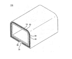
図1は、本発明の第1実施形態に係る電気接触端子100を示す。
図1を参照すると、弾性電気接触端子100は、チューブ状の絶縁弾性コア(core:10)、絶縁非発泡ゴムコーティング層20及び一面に金属層40が形成された耐熱ポリマーフィルム30が順次積層されてなる。
Hereinafter, embodiments of the present invention will be described in detail with reference to the accompanying drawings.
-1st Embodiment FIG. 1: shows the
Referring to FIG. 1, an elastic
このような構造によると、圧出で製造されたチューブ状の弾性コアを適用することにより、製造コストが低くなり、チューブの貫通穴の大きさを調節して弾性及び押圧される力を調節でき、また、小さいサイズの製品の製造も困難ではない。また、絶縁非発泡コーティング層を適用することにより、半田付け前後に接着力と弾性が維持され、繰り返される圧縮試験でも接着力と弾性が維持される。また、金属層が形成された耐熱ポリマーフィルムを適用することによって、耐熱ポリマーフィルムにて半田付け条件を満たし、柔軟性が良く、圧縮試験でも弾性を維持し、金属層により半田クリームによる半田付けが可能である。 According to such a structure, by applying a tube-shaped elastic core manufactured by extruding, the manufacturing cost is reduced, and the size of the through hole of the tube can be adjusted to adjust the elasticity and the pressing force. In addition, it is not difficult to manufacture a small size product. Further, by applying the insulating non-foaming coating layer, the adhesive force and elasticity are maintained before and after soldering, and the adhesive force and elasticity are maintained even in repeated compression tests. Also, by applying a heat-resistant polymer film with a metal layer formed, the heat-resistant polymer film satisfies the soldering conditions, has good flexibility, maintains elasticity even in a compression test, and the metal layer can be soldered with a solder cream. Is possible.
・ 1 絶縁弾性コア10
図1を参照すると、最内部に位置する絶縁弾性コア10は、チューブまたはチューブ状であって、この実施形態では、端面が四角形をなす。しかしながら、これに限定されず、絶縁弾性コア10の端面は、様々な形状をなすように圧出できる。好ましくは、絶縁弾性コア10の端面において、両側壁の厚さは、上下壁の厚さより薄く形成することにより弾性を良くし、押圧される力を少なくすることができる。
・ 1 Insulating
Referring to FIG. 1, the insulating
絶縁弾性コア10の材質は、リフロー半田付け及び弾性条件を満たすために、非発泡耐熱弾性ゴム、例えば、シリコンゴムであることが好ましい。
The material of the insulating
また、絶縁弾性コア10材料の硬度は、適当な機械的強度及び弾性のため、Shore A 40〜70が好ましい。
Further, the hardness of the insulating
また、絶縁弾性コア10の上面両側周縁部は、各々ラウンド状(丸みを帯びた形成)で形成できる。このような構造によると、取り扱いが容易であるだけではなく、完成された電気接触端子100が印刷回路基板などに半田付けされた後、対向する対象物と組み合わされる過程において、両側面におけるひっかかりを防止できる。
Further, the peripheral edge portions on both sides of the upper surface of the insulating
また、絶縁弾性コア10の色合いは、金属層40の色合いと異なるのが好ましい。
Further, the color of the insulating
1.2 絶縁非発泡ゴムコーティング層20
絶縁非発泡ゴムコーティング層20は、弾性コア10と耐熱ポリマーフィルム30表面間に位置し、弾性コア10と耐熱ポリマーフィルム30を信頼性良く接着する。更に、絶縁非発泡ゴムコーティング層20は、半田付け前後にも接着力を維持し、常に弾性を維持しなければならない。好ましくは、柔軟性及び弾性のため、完全に硬化された絶縁非発泡ゴムコーティング層20の硬度は、Shore A 20〜60であり、厚さは、約0.02〜0.2mmである。
1.2 Insulating non-foamed
The insulating non-foamed
絶縁非発泡ゴムコーティング層20は、液状シリコンゴムを硬化することにより形成でき、その種類としては、熱により硬化されるシリコンゴムまたは湿気により硬化されるシリコンゴムなどから選択されて使用される。好ましくは、作業速度を高めるため、熱により完全に硬化するタイプを使用できる。
The insulating non-foamed
前記の液状シリコンゴムは、硬化しながら対向する対象物と接着を有し、硬化後、固状の絶縁非発泡ゴムコーティング層20で形成され、一度硬化された後は弾性を維持し、再び熱が加わっても接着力を維持する。好ましくは、信頼性ある接着力を得るため、液状のシリコンゴムに接着力強化剤を添加するか、または接着しようとする対象物、即ち、弾性コア10または耐熱ポリマーフィルム30の表面にコロナ処理などの表面処理を行う。
The liquid silicone rubber has an adhesion to an opposing object while being cured, and is formed by a solid insulating non-foamed
好ましくは、液状のシリコンゴムにフェライトなどの磁性パウダーや圧電パウダーを混ぜて硬化後、絶縁非発泡ゴムコーティング層20が磁性または圧電特性を有するようにできる。この場合、金属層40に流れる電流のノイズを除去できる。
Preferably, the insulating non-foamed
1.3 耐熱ポリマーフィルム30
耐熱ポリマーフィルム30は、例えば、耐熱性の良いポリイミド(PI)フィルムやその他の耐熱ポリマーフィルムであり、その厚さは、柔軟性及び機構的強度を考え、例えば、0.01〜0.05mm間で形成されるのが好ましい。
1.3 Heat
The heat-
また、耐熱ポリマーフィルム30の裏面には、金属層40が一体に形成される。この時、金属層40の一定部位をエッチング作業により除去することにより、耐熱ポリマーフィルム30の柔軟性を向上するか、またはエッチングにより金属層40を電気的に絶縁された多数の部分に分割し、弾性電気接触端子が半田付けされる接地パターンを多数の部分それぞれに対応するように絶縁間隙を有する多数の接地パターンに分割することにより、1つの電気接触端子100を多数の電気接触端子として使用できる。
A
好ましくは、金属層40は、多数の金属層でなり、好ましくは、金属層40は、耐熱ポリマーフィルム30上に金属をスパッタリングした後、その上に、金属を鍍金したものである。好ましくは、金属層40の一層は、銅鍍金により形成され、全体的な金属層40の主成分は、銅である。金属層40の最外郭表面は、腐食防止及び半田クリームによる半田付けが良くなるように、すず、銀または金の何れかを含む。好ましくは、金属層40が耐熱ポリマーフィルムとの強い接着力、優れた電気伝導度及び強い半田付け強度を有するため、耐熱ポリマーフィルム上に金属をスパッタリングコーティングした後、その上に銅鍍金を行い、その上に、すずを鍍金する。金属層40の厚さは、柔軟性や半田付け性及び半田付け強度などを考え、例えば、0.002〜0.01mm間で形成できる。
Preferably, the
一方、金属層40が形成された耐熱ポリマーフィルム30は、一例として端面軟性積層金属板(FCCL)である。
On the other hand, the heat
・ 4 電気接触端子100の製造方法
以下、前記の電気接触端子100の製造方法に対して説明する。
4. Method for Manufacturing
裏面に金属層40が形成された一定幅を有する耐熱ポリマーフィルム30の絶縁された表面上に熱により硬化される液状シリコンゴムをキャスティング(Casting)機械で厚さ0.02mm〜0.2mmにキャスティングし、液状シリコンゴムコーティング層を形成しながら、このコーティング層上に圧出工程によりロール(roll)形態で製造された弾性コア10を載せ、一定形状のジグにより囲む。
A liquid silicon rubber cured by heat is cast to a thickness of 0.02 mm to 0.2 mm by a casting machine on the insulated surface of the heat-
ここで、液状シリコンゴムのコーティング層の厚さが薄すぎると、弾性コア10と耐熱ポリマーフィルム30との間の接着力が悪くなり、コーティング層の厚さが厚すぎると、液状のシリコンゴムが硬化するのに時間がかかるという欠点がある。もし、湿気により硬化される液状シリコンゴムでコーティング層を形成する場合は、窒素もしくは真空雰囲気でコーティングするのが好ましい。
Here, if the coating layer of the liquid silicone rubber is too thin, the adhesive force between the
以後、弾性コア10を囲む耐熱ポリマーフィルム30を弾性コア10の寸法と類似の寸法を有する金型に位置させ、弾性コア10と耐熱ポリマーフィルム30の間に介在された液状のシリコンゴムコーティング層を熱により硬化させると、液状のシリコンゴム層は、硬化されながら絶縁非発泡ゴムコーティング層20に変化する。この時、絶縁非発泡ゴムコーティング層20は、弾性コア10と耐熱ポリマーフィルム30を接着する役割をする。即ち、液状のシリコンコーティング層は、一定寸法の高温の金型内部及び外部で熱硬化後、弾性コア10と耐熱ポリマーフィルム30を接着させる接着剤の役割をしながら弾性を有する絶縁非発泡ゴムコーティング層20になる。
Thereafter, the heat-
液状のシリコンゴムは、一度硬化されると、熱により再度溶融されないため、電気接触端子100を半田付けする時にも、元の接着性能を維持する。この時、金型内部に位置した液状シリコンゴムの硬化速度を速くするため、金型の温度を約180℃程度に維持し、周辺の湿度を60%程度に維持する。
Once the liquid silicone rubber is cured, it is not melted again by heat, so that the original adhesive performance is maintained even when the
更に、電気接触端子100は、裏面に金属層40が形成された耐熱ポリマーフィルム30を使用して製造するため、長さの長い製品は、しわむなどの問題があり、通常1m以下の長さで製造した後、最終的に必要とする長さである3mm〜30mm長さで切断して使用する。また、湿気と熱により同時に硬化される液状シリコンゴムを使用すると、硬化時間を短縮できる。
Furthermore, since the
このように作製された電気接触端子100の外部表面は、金属層40でなり、電気伝導度が0.01Ω以下で非常に良く、半田付けが良くなり、半田付け強度が良い。この実施形態において、金属層40は、スパッタリング及び電解鍍金により形成されたものを使用し、金属層40は、すずで鍍金された銅が主成分であり、耐熱ポリマーフィルム30は、ポリイミド(PI)を使用し、弾性コア10と絶縁非発泡ゴムコーティング層20は、シリコンゴムを使用したため、半田付け前後において元の固有性能を維持する。また、半田付け前後において電気伝導度が良く、弾性回復力が優れる。
The external surface of the
好ましくは、耐熱ポリマーフィルム30の底面は、印刷回路基板と半田付けが良くなる構造を有し、上面の一部は、水平をなすようにすることによって、真空ピックアップによる表面実装によるリフロー半田付けが可能となる。
Preferably, the bottom surface of the heat-
・ 第2実施形態
図2は、本発明の第2実施形態に係る電気接触端子110を示す。
Second Embodiment FIG. 2 shows an
図2を参照すると、絶縁弾性コア10の下面は、幅方向に、両端から中間部分に向けて凹んだ形状となるように傾けて形成する。傾き角度θは、シリコンゴムの物性値(例えば、熱膨張率)及び寸法によって変わり、例えば、1°〜10°の角度範囲内で形成されるのが好ましい。
Referring to FIG. 2, the lower surface of the insulating
このような構造によると、絶縁弾性コア10の下面が両端から中間部分に向けて凹んだ形状をするため、印刷回路基板に表面実装される時、接地パターン上に塗布した半田クリームが凹んだ部分を満たすことになり、絶縁弾性コア10の下面両端が浮き上がることなく半田クリームと信頼性良く装着される。また、これにより、金属層40の両側面から半田立ち上がり現象が増大され、半田付け強度が更に向上され、一方に浮き上がることなどを防止できる。
According to such a structure, since the bottom surface of the insulating
・ 第3実施形態
図3は、本発明の第3実施形態に係る電気接触端子120を示す。
Third Embodiment FIG. 3 shows an
図3を参照すると、耐熱ポリマーフィルム30の両端は、一定間隔で離隔されて受容空間32を形成し、絶縁非発泡ゴムコーティング層20に接着される。このような構造によると、液状の絶縁非発泡ゴムコーティング層20が形成された耐熱ポリマーフィルム30が金型(図示せず)を通過しながら圧着され、熱硬化により接着される場合、金型による外部圧力により耐熱ポリマーフィルム30の両端からはみ出す液状の絶縁非発泡ゴムコーティング層20の漏出物21が、離隔された耐熱ポリマーフィルム30の両端により形成される受容空間32に受容される。
Referring to FIG. 3, both ends of the heat-
よって、硬化後、金属層40外側にはみ出した固状の絶縁非発泡ゴムコーティング層20の漏出物21により金属層40の半田付けが妨害されるのが防止される。また、半田付けされない漏出物21が受容空間32に受容され、電気接触端子120がPCB上で半田付けされる時、浮き上がる現象などが防止され、半田付け強度を増加させる。
Therefore, the soldering of the
好ましくは、このような受容空間32は、絶縁弾性コア10の下面中央を基準に左右対称に形成され、リフロー半田付け後、電気接触端子120の左右側面の半田付け強度が同程度となるようにする。また、これら受容空間32により電気接触端子100の上面と下面が区別できる。好ましくは、受容空間32の幅は、電気接触端子120の幅により異なることもあるが、0.1mm以上である。このように受容空間32部位には、高価の金属層が形成されたポリマーフィルム30が付着されていないため、コスト低減に役に立つ。
Preferably, the receiving
更に、半田クリームは、金属層40にのみ半田付けされるので、受容空間32に存在する半田クリームは、半田付け中に金属層40の両側面に移動されるため、半田付け強度が強くなるという利点もある。
Further, since the solder cream is soldered only to the
特に、前記の第2実施形態のように、絶縁弾性コア10の下面を幅方向に両端から中間部分に向けて凹んだ形状となるように傾けて形成し、ここに受容空間32を形成する場合、実質的に絶縁非発泡ゴムコーティング層20の漏出物21を受容できる空間を更に増加できる。
In particular, as in the second embodiment, the lower surface of the insulating
また、このような構造によると、受容空間32により電気接触端子120の上面と下面が明確に区別でき、真空ピックアップによるリール舗装の時、便利である。
Moreover, according to such a structure, the upper surface and the lower surface of the
・ 第4実施形態
図4は、本発明の第4実施形態に係る電気接触端子130を示す。
-4th Embodiment FIG. 4: shows the
図4を参照すると、弾性コア10の底面に金属補強台50を位置させた後、弾性コア10と金属補強台50を含む全体を絶縁非発泡ゴムコーティング層20を介在して裏面に金属層40が形成された耐熱ポリマーフィルム30で囲む。この時、耐熱ポリマーフィルム30の両端を互いに離隔させ、隙間34を形成する。
Referring to FIG. 4, after the
この実施形態によると、印刷回路基板に表面実装の時、半田クリームが間隙34により金属補強台50と接触し、半田付けした後、強い接着力を有するという利点がある。また、間隙34により電気接触端子130の上部と下部の区別が容易であり、軽い製品の場合、金属補強台50の自重により真空ピックアップによる表面実装時に供給される風によっても容易に動かないという利点がある。
According to this embodiment, when the surface mounting is performed on the printed circuit board, the solder cream comes into contact with the
・ 第5実施形態
図5は、本発明の第5実施形態に係る電気接触端子140を示す。
-5th Embodiment FIG. 5: shows the
絶縁弾性コア10は、内部に貫通穴15が形成されたチューブ状であって、端面は、略四角形や円形で形成できるが、これに限定されなく、多様な形状をなすように圧出工程により提供される。
The insulating
上記のように、絶縁弾性コア10材料の硬度は、適当な機械的強度及び弾性のため、Shore A40〜70が好ましく、絶縁弾性コア10の上面の押圧力は、内部に形成された貫通穴15の大きさ及び形状により決定される。
As described above, the hardness of the material of the insulating
絶縁弾性コア10の内部に形成される貫通穴15は、絶縁弾性コア10の重量中心が下部に形成できるように、絶縁弾性コア10の上部に偏って形成されるのが好ましい。即ち、図5を参照すると、絶縁弾性コア10の下部部分11は、他の部分12、13に比べずっと厚く形成することにより、結果的に貫通穴15は上部に偏る。このような構造によると、絶縁弾性コア10の重量中心が下部に形成されることにより、リール舗装の時、振動により上下面の整列が可能であり、リフロー半田付けのときに動きが少ない。更に、絶縁弾性コア10の下部部分11の厚い厚さは、自体重量を増大させ、また、外部の圧力により一定水準にまで押圧される役割をし、対向する対象物と接触の時、上部部分12が可能な限り水平をなすようにする。好ましくは、絶縁弾性コア10の厚さは、下部部分11が最も厚く、押圧力を少なくするため、且つ、上部部分12が平行をなすように、両側部分13が最も薄い。
The through
絶縁弾性コア10の内部を貫通する貫通穴15は、四角形または多角形であるが、円形または楕円形でも形成できる、好ましくは、四角形で形成する。
The through
貫通穴15が四角形をなす場合、貫通穴15の両側部分13は、上部側にいくほど狭くなる形状で、対称をなして傾き、これに対応して絶縁弾性コア10の外側面も同一に傾くように形成できる。このような構造によると、絶縁弾性コア10の上面に接触する対象物から加わる圧力が絶縁弾性コア10の両側面外部に分散され、貫通穴15が形成された絶縁弾性コア10の上部が一方に傾くことなどを防止できる。
When the through
また、貫通穴15の上部部分12と下部部分11は、各々その中間にそれぞれ上部及び下部突出部16、17が形成されるように傾く。このような構造によると、上部突出部16により絶縁弾性コア10の上部部分12が補強されながら上面に加わる圧力により上部部分12の中心部が陥没されず平面を維持できる。また、下部突出部17は、絶縁弾性コア10の下部部分11に重さが集中できるようにし、上部突出部16と接して貫通穴15が変形される高さを制限する役割をする。
Further, the
好ましくは、絶縁弾性コア10の貫通穴15の両側部分13の厚さを上部及び下部部分11、12の厚さより薄く形成することによって、上部からの押圧弾性をよくすることができる。
Preferably, by forming the thickness of both
・ 第6実施形態
図6は、本発明の第6実施形態に係る電気接触端子を示し、図7は、図6の電気接触端子の実際使用例を示す。
-6th Embodiment FIG. 6: shows the electrical contact terminal which concerns on 6th Embodiment of this invention, and FIG. 7 shows the actual usage example of the electrical contact terminal of FIG.
図6を参照すると、絶縁弾性コア10の下面に長手方向に形成され、耐熱ポリマーフィルム30の両端間に位置した受容溝24が形成される。このような受容溝24は、上記の受容空間32と共に更に多い量の絶縁非発泡ゴムコーティング層20の漏出物を受容でき、半田付け強度を増大し、絶縁非発泡ゴムコーティング層20が多量で使用される大きいサイズの製品に適切に使用できる。
Referring to FIG. 6, a receiving
このような受容溝24は、絶縁弾性コア10を製造する圧出工程において、金型ダイ(Die)により形成されるため、絶縁弾性コア10下面が左右対称をなすように中央部位に形成できる。
Since the receiving
よって、弾性コア10の中央に位置した受容溝24により耐熱ポリマーフィルム30の両端にて形成された受容空間32が絶縁弾性コア10の下面中央に位置することを助け、半田付けの時、一方に浮き上がる現象が減少する。好ましくは、受容溝24の幅は、0.2mm〜2mmであり、最大幅は、0.2mm〜2mmであり、V状またはU状をなす。好ましくは、受容空間32の幅は、上記のように、0.1mm以上である。
Therefore, the receiving
図8は、前記の電気接触端子100が印刷回路基板1に表面実装される一例を示す。この例は、上記のように、弾性電気接触端子100が半田付される接地パターン及び半田クリームを、絶縁間隙を有する多数の接地パターン及び半田クリームに分割することにより、1つの電気接触端子100が多数の接地パターン上に半田付けされる。
FIG. 8 shows an example in which the
電気接触端子100の金属層40は、接地パターン2、2a上に半田クリーム3、3aを介在して付着される。この時、印刷回路基板1上に形成される接地パターン2、2aと半田クリーム3、3aは、電気接触端子100が浮き上がる現象と傾く現象を防止するために、一定間隔で分割形成される。例えば、図8では、電気接触端子100の長手方向に2等分されたが、電気接触端子100の幅方向に分割でき、長手方向と幅方向全てで分割できる。
The
好ましくは、分割された各接地パターン2、2a及び半田クリームパターン3、3aの大きさ及び模様が、互いに対称となるように等分割でなすことができ、大きさは、電気接触端子100の幅と長さより大きい。
Preferably, the divided
また、接地パターン2、2a及び半田クリーム3、3aの分割間隔は、半田付け強度向上及び浮き上がる現象を少なくするため、また、コスト低減のため、1mm以上が好ましいが、電気接触端子100の長さや幅に対して5%〜20%以内で形成されるのが好ましい。
Further, the interval between the
図8に示すように、半田クリーム3、3aは、有機溶剤(Flux)と導電性金属パウダーが混合されているものであって、分割された各接地パターン2、2aの表面に塗布される。
As shown in FIG. 8, the
このような接地パターン及び半田クリームパターンを適用することにより、電気接触端子100の底面が平面ではなくても、半田クリームパターンに安定的に実装されて半田付けされ、体積に比べて重さが軽い電気接触端子100を半田クリームパターンに安定的に実装でき、半田クリームの使用量を減らすことができる。更に、このような分割されたパターンにより、ねじれる現象や浮き上がる現象が減少する。
By applying such a ground pattern and solder cream pattern, even if the bottom surface of the
一方、好ましくは、接地パターン2、2aに対向する金属層40には、耐熱両面粘着テープ110が付着できる。耐熱両面粘着テープ110は、ポリイミドフィルム112の表面と裏面にそれぞれ耐熱粘着剤114、116がコーティングされた構造を備える。ここで、耐熱粘着剤としては、シリコンゴム系粘着剤が用いられる。
On the other hand, preferably, the heat-resistant double-sided
このような構造によると、電気接触端子100が真空ピックアップにより半田クリーム3、3a上に実装される時、半田付けに先立って耐熱両面粘着テープ110が接地パターン2,2a間の印刷回路基板1に直接粘着されるため、リフロー半田付けの時、電気接触端子100がねじれる現象を防止する。
According to such a structure, when the
ここで、耐熱両面粘着テープ110は、受容空間が形成されていない第1実施形態を含み、第2〜第4実施形態に全て適用できる。
Here, the heat-resistant double-sided
以上では、本発明の一実施形態を中心として説明したが、当業者であれば、多様な変更・変形を加えることができる。このような変更・変形が、本発明の範囲を逸脱しない限り、本発明に属するといえる。本発明の権利範囲は、請求の範囲により判断されるべきである。 In the above, one embodiment of the present invention has been mainly described. However, those skilled in the art can make various changes and modifications. It can be said that such changes and modifications belong to the present invention as long as they do not depart from the scope of the present invention. The scope of the present invention should be determined by the claims.
本発明の弾性電気接触端子によれば、対象物と印刷回路基板を電気的及び機構的に連結しながら半田付けすることが可能であり、生産効率向上に有用である。 According to the elastic electrical contact terminal of the present invention, the object and the printed circuit board can be soldered while being electrically and mechanically connected, which is useful for improving the production efficiency.
1 印刷回路基板
2 接地パターン
3 半田クリーム
10 弾性コア
11 下部部分
12 上部部分
13 両側部分
15 貫通穴
16 上部突出部
17 下部突出部
20 絶縁非発泡ゴムコーティング層
24 受容溝
30 耐熱ポリマーフィルム
32 受容空間
34 間隙
40 金属層
100 電気接触端子
110 電気接触端子
112 ポリイミドフィルム
114 耐熱粘着剤
120 電気接触端子
130 電気接触端子
140 電気接触端子
DESCRIPTION OF SYMBOLS 1 Printed
Claims (16)
前記絶縁弾性コアを囲んで接着される絶縁非発泡ゴムコーティング層と、
一面は前記絶縁非発泡ゴムコーティング層を囲むように前記絶縁非発泡ゴムコーティング層に接着され、他面は金属層が一体に形成された耐熱ポリマーフィルムを含み、
前記絶縁弾性コアの下面は、幅方向に、両端から中間部分に向けて凹んだ形状となるように傾けて形成される、半田付け可能な弾性電気接触端子。 An insulating elastic core having a through-hole formed therein in the longitudinal direction ;
An insulating non-foamed rubber coating layer bonded around the insulating elastic core;
One surface is adhered to the insulating non-foam rubber coating layer to surround the insulating non-foam rubber coating layer, the other surface is viewed contains a heat-resistant polymer film a metal layer is formed integrally,
The bottom surface of the insulating elastic core is a solderable elastic electrical contact terminal formed so as to be inclined in a width direction so as to be recessed from both ends toward an intermediate portion .
前記絶縁弾性コアを囲んで接着される絶縁非発泡ゴムコーティング層と、
一面は前記絶縁非発泡ゴムコーティング層を囲むように前記絶縁非発泡ゴムコーティング層に接着され、他面は金属層が一体に形成された耐熱ポリマーフィルムを含み、
前記耐熱ポリマーフィルムは、両端が離隔されるように、前記絶縁非発泡ゴムコーティング層に接着され、前記絶縁非発泡ゴムコーティング層に前記耐熱ポリマーフィルムが接着時、前記耐熱ポリマーフィルムの両端からはみ出す前記絶縁非発泡ゴムコーティング層の漏出物が、前記離隔された耐熱ポリマーフィルムの両端により形成された受容空間に受容される、半田付け可能な弾性電気接触端子。 An insulating elastic core having a through-hole formed therein in the longitudinal direction;
An insulating non-foamed rubber coating layer bonded around the insulating elastic core;
One surface is bonded to the insulating non-foamed rubber coating layer so as to surround the insulating non-foamed rubber coating layer, and the other surface includes a heat-resistant polymer film integrally formed with a metal layer,
The heat-resistant polymer film is bonded to the insulating non-foamed rubber coating layer so that both ends are separated from each other, and the heat-resistant polymer film protrudes from both ends of the heat-resistant polymer film when the heat-resistant polymer film is bonded to the insulating non-foamed rubber coating layer. A solderable elastic electrical contact terminal in which leakage of an insulating non-foamed rubber coating layer is received in a receiving space formed by both ends of the separated heat-resistant polymer film.
前記耐熱両面粘着テープは、印刷回路基板に直接粘着される、請求項1または2に記載の半田付け可能な弾性電気接触端子。 A heat-resistant double-sided adhesive tape is attached to a part of the bottom surface of the metal layer,
The solderable elastic electrical contact terminal according to claim 1 , wherein the heat-resistant double-sided adhesive tape is directly adhered to a printed circuit board.
Applications Claiming Priority (6)
| Application Number | Priority Date | Filing Date | Title |
|---|---|---|---|
| KR10-2008-0021640 | 2008-03-07 | ||
| KR1020080021640A KR100839893B1 (en) | 2008-03-07 | 2008-03-07 | Solderable elastic electric contact terminal |
| KR20-2008-0005393 | 2008-04-23 | ||
| KR2020080005393U KR200442316Y1 (en) | 2008-04-23 | 2008-04-23 | Assembly of Electric Contact Terminal Having Insulated Elastic Body |
| KR10-2008-0063460 | 2008-07-01 | ||
| KR1020080063460A KR101001354B1 (en) | 2008-07-01 | 2008-07-01 | Reflow solderable electric contacts having elasticity |
Publications (2)
| Publication Number | Publication Date |
|---|---|
| JP2009218207A JP2009218207A (en) | 2009-09-24 |
| JP4733752B2 true JP4733752B2 (en) | 2011-07-27 |
Family
ID=40791589
Family Applications (1)
| Application Number | Title | Priority Date | Filing Date |
|---|---|---|---|
| JP2009045556A Active JP4733752B2 (en) | 2008-03-07 | 2009-02-27 | Solderable elastic electrical contact terminals |
Country Status (8)
| Country | Link |
|---|---|
| US (1) | US7931475B2 (en) |
| EP (1) | EP2099269B1 (en) |
| JP (1) | JP4733752B2 (en) |
| AT (1) | ATE555644T1 (en) |
| CA (1) | CA2653315C (en) |
| MY (1) | MY147054A (en) |
| PL (1) | PL2099269T3 (en) |
| TW (1) | TWI387159B (en) |
Cited By (1)
| Publication number | Priority date | Publication date | Assignee | Title |
|---|---|---|---|---|
| KR101503307B1 (en) * | 2014-09-25 | 2015-03-19 | 주식회사 이송이엠씨 | Thermal conductive elastomer defending antenna effect by noise coupling |
Families Citing this family (30)
| Publication number | Priority date | Publication date | Assignee | Title |
|---|---|---|---|---|
| KR101054251B1 (en) * | 2009-05-18 | 2011-08-08 | 두성산업 주식회사 | Conductive Contact Terminals for Board Surface Mount |
| KR100993253B1 (en) * | 2010-04-28 | 2010-11-10 | 김선기 | Elastic electric contact terminal |
| JP5745792B2 (en) * | 2010-08-02 | 2015-07-08 | 矢崎総業株式会社 | Fixing bracket for components mounted on circuit board |
| KR101048083B1 (en) * | 2010-10-14 | 2011-07-11 | 주식회사 이노칩테크놀로지 | Emi shielding gasket |
| KR101033193B1 (en) * | 2010-10-14 | 2011-05-06 | 주식회사 이노칩테크놀로지 | Emi shielding gasket |
| KR101084282B1 (en) | 2011-06-15 | 2011-11-17 | 김선기 | Solderable elastic electric contact terminal |
| DE102012100598A1 (en) * | 2012-01-25 | 2013-07-25 | Eugen Forschner Gmbh | Sealed plug and method for sealing a plug |
| DE212013000167U1 (en) * | 2012-07-28 | 2015-03-06 | Laird Technologies, Inc. | Metallic film coated foam contact |
| US9531853B2 (en) * | 2013-03-14 | 2016-12-27 | Htc Corporation | Electronic module and electronic device |
| WO2015006438A1 (en) | 2013-07-09 | 2015-01-15 | United Technologies Corporation | Plated polymer compressor |
| EP3019711B1 (en) | 2013-07-09 | 2023-11-01 | RTX Corporation | Plated polymer nosecone |
| EP3019710A4 (en) | 2013-07-09 | 2017-05-10 | United Technologies Corporation | Plated polymer fan |
| US9789664B2 (en) | 2013-07-09 | 2017-10-17 | United Technologies Corporation | Plated tubular lattice structure |
| WO2015006400A1 (en) * | 2013-07-09 | 2015-01-15 | United Technologies Corporation | Plated polymeric wind turbine components |
| JP5736418B2 (en) * | 2013-07-16 | 2015-06-17 | 星和電機株式会社 | Soft electrical conductor |
| EP2874233B1 (en) * | 2013-11-14 | 2017-01-25 | Joinset Co., Ltd | Surface-mount type electric connecting terminal, and electronic module unit and circuit board using the same |
| CN105390850B (en) * | 2014-08-22 | 2017-12-29 | 卓英社有限公司 | The surface-pasted bladder type electric contact terminal of Reflow Soldering can be achieved with |
| KR101600510B1 (en) * | 2014-08-22 | 2016-03-07 | 조인셋 주식회사 | Pocket-typed electric contact terminal capable for surface mounting with reflow soldering process |
| TWI559641B (en) * | 2015-01-20 | 2016-11-21 | 群創光電股份有限公司 | Display device |
| KR101711016B1 (en) * | 2015-03-23 | 2017-02-28 | 조인셋 주식회사 | Elastic electric contact terminal having improved environmental property and Method for making the same |
| US20160336093A1 (en) * | 2015-05-15 | 2016-11-17 | Joinset Co., Ltd. | Elastic electric contact terminal adapted to small size |
| KR102350393B1 (en) * | 2015-07-31 | 2022-01-14 | 엘지디스플레이 주식회사 | Electromagnetic wave shielding structure and display device having the same |
| WO2017026625A1 (en) | 2015-08-07 | 2017-02-16 | 조인셋 주식회사 | Electrical connecting terminal |
| KR101793717B1 (en) | 2015-08-07 | 2017-11-03 | 조인셋 주식회사 | Electric Connecting Terminal |
| CN206619706U (en) * | 2017-04-14 | 2017-11-07 | 深圳市卓汉材料技术有限公司 | One kind ground connection elastic component |
| KR102026465B1 (en) * | 2017-11-10 | 2019-09-27 | 조인셋 주식회사 | Electric connecting terminal for metal case |
| US10270193B1 (en) * | 2017-12-18 | 2019-04-23 | Continental Automotive Systems, Inc. | Concentric springs for sensor connection |
| US11439832B2 (en) * | 2019-01-09 | 2022-09-13 | Stimwave Technologies Incorporated | Implantable electronic devices |
| KR102236798B1 (en) * | 2019-05-21 | 2021-04-06 | 조인셋 주식회사 | Elastic electric connect terminal assembly |
| KR102416027B1 (en) * | 2019-11-15 | 2022-07-05 | 조인셋 주식회사 | Elastic electrical contact terminal |
Citations (3)
| Publication number | Priority date | Publication date | Assignee | Title |
|---|---|---|---|---|
| JPH1013010A (en) * | 1996-06-27 | 1998-01-16 | Fuji Photo Film Co Ltd | Method for fixing electronic component and electronic component used for it |
| JP2001326478A (en) * | 2000-05-12 | 2001-11-22 | Kitagawa Ind Co Ltd | Conducting member |
| JP2008014942A (en) * | 2006-07-03 | 2008-01-24 | Zippertubing (Japan) Ltd | Elastic electric contact terminal which can be soldered |
Family Cites Families (20)
| Publication number | Priority date | Publication date | Assignee | Title |
|---|---|---|---|---|
| US3638163A (en) * | 1970-07-20 | 1972-01-25 | Bell Telephone Labor Inc | Connector for electrically interconnecting two parallel surfaces |
| US4601963A (en) * | 1983-04-15 | 1986-07-22 | Ricoh Company, Ltd. | Locally deformable photosensitive drum for use in electrophotography |
| JPH062174Y2 (en) * | 1985-07-23 | 1994-01-19 | 古河電気工業株式会社 | Water-blocking rubber, plastic insulated power cable |
| US4857668A (en) * | 1988-04-15 | 1989-08-15 | Schlegel Corporation | Multi-function gasket |
| FR2652228B1 (en) * | 1989-09-19 | 1996-05-24 | Bull Sa | SHIELDING CHASSIS FOR THE PROTECTION AGAINST THE EFFECTS OF ELECTROMAGNETIC RADIATION, OF AN ELECTRICAL CIRCUIT PLACED WITHIN THIS CHASSIS. |
| US5597652A (en) * | 1990-01-12 | 1997-01-28 | Bridgestone Corporation | Conductive roll |
| US5578527A (en) * | 1995-06-23 | 1996-11-26 | Industrial Technology Research Institute | Connection construction and method of manufacturing the same |
| JPH1068849A (en) * | 1996-08-29 | 1998-03-10 | Tokin Corp | Optical fiber cable |
| US6002589A (en) * | 1997-07-21 | 1999-12-14 | Rambus Inc. | Integrated circuit package for coupling to a printed circuit board |
| US6255581B1 (en) | 1998-03-31 | 2001-07-03 | Gore Enterprise Holdings, Inc. | Surface mount technology compatible EMI gasket and a method of installing an EMI gasket on a ground trace |
| JP2000259027A (en) * | 1999-03-09 | 2000-09-22 | Canon Inc | Fixing device |
| TW525273B (en) * | 2002-02-07 | 2003-03-21 | Via Tech Inc | Elastomer interposer for fixing package onto printed circuit board and fabrication method thereof |
| US7129421B2 (en) | 2002-12-06 | 2006-10-31 | Gore Enterprise Holdings, Inc. | Soft surface mount technology compatible EMI gasket |
| FR2876493B1 (en) * | 2004-10-12 | 2007-01-12 | F S P One Soc Par Actions Simp | COPPER ALUMINUM TORONIC CABLE AND METHOD FOR MANUFACTURING THE SAME |
| KR200390490Y1 (en) | 2005-05-02 | 2005-07-21 | 조인셋 주식회사 | SMD Typed Electrical contact terminal |
| JP4635783B2 (en) * | 2005-08-24 | 2011-02-23 | 富士ゼロックス株式会社 | Fixing device, image forming apparatus |
| JP4951990B2 (en) * | 2006-02-13 | 2012-06-13 | 富士ゼロックス株式会社 | Elastic body roll and fixing device |
| JP2008021637A (en) * | 2006-06-12 | 2008-01-31 | Fujikura Ltd | Socket, its manufacturing method, and semiconductor device |
| KR200428000Y1 (en) * | 2006-07-03 | 2006-10-04 | 조인셋 주식회사 | Solderable Electric contact terminal |
| KR100783588B1 (en) | 2006-11-08 | 2007-12-07 | 조인셋 주식회사 | Solderable electric contact terminal |
-
2009
- 2009-02-06 MY MYPI20090470A patent/MY147054A/en unknown
- 2009-02-09 CA CA2653315A patent/CA2653315C/en active Active
- 2009-02-11 EP EP09001910A patent/EP2099269B1/en active Active
- 2009-02-11 AT AT09001910T patent/ATE555644T1/en active
- 2009-02-11 PL PL09001910T patent/PL2099269T3/en unknown
- 2009-02-25 TW TW098105965A patent/TWI387159B/en active
- 2009-02-26 US US12/393,948 patent/US7931475B2/en active Active
- 2009-02-27 JP JP2009045556A patent/JP4733752B2/en active Active
Patent Citations (3)
| Publication number | Priority date | Publication date | Assignee | Title |
|---|---|---|---|---|
| JPH1013010A (en) * | 1996-06-27 | 1998-01-16 | Fuji Photo Film Co Ltd | Method for fixing electronic component and electronic component used for it |
| JP2001326478A (en) * | 2000-05-12 | 2001-11-22 | Kitagawa Ind Co Ltd | Conducting member |
| JP2008014942A (en) * | 2006-07-03 | 2008-01-24 | Zippertubing (Japan) Ltd | Elastic electric contact terminal which can be soldered |
Cited By (1)
| Publication number | Priority date | Publication date | Assignee | Title |
|---|---|---|---|---|
| KR101503307B1 (en) * | 2014-09-25 | 2015-03-19 | 주식회사 이송이엠씨 | Thermal conductive elastomer defending antenna effect by noise coupling |
Also Published As
| Publication number | Publication date |
|---|---|
| ATE555644T1 (en) | 2012-05-15 |
| PL2099269T3 (en) | 2012-09-28 |
| JP2009218207A (en) | 2009-09-24 |
| US7931475B2 (en) | 2011-04-26 |
| TWI387159B (en) | 2013-02-21 |
| CA2653315A1 (en) | 2009-09-07 |
| EP2099269A1 (en) | 2009-09-09 |
| CA2653315C (en) | 2011-12-20 |
| EP2099269B1 (en) | 2012-04-25 |
| TW200941841A (en) | 2009-10-01 |
| US20090227127A1 (en) | 2009-09-10 |
| MY147054A (en) | 2012-10-15 |
Similar Documents
| Publication | Publication Date | Title |
|---|---|---|
| JP4733752B2 (en) | Solderable elastic electrical contact terminals | |
| CN101527400B (en) | Solderable elastic electric contact terminal | |
| US8461455B2 (en) | Elastic electric contact terminal | |
| KR100892720B1 (en) | Solderable elastic electric contact terminal | |
| KR101001354B1 (en) | Reflow solderable electric contacts having elasticity | |
| KR101084282B1 (en) | Solderable elastic electric contact terminal | |
| JP4427565B2 (en) | Solderable elastic electrical contact terminals | |
| KR101711016B1 (en) | Elastic electric contact terminal having improved environmental property and Method for making the same | |
| KR101087189B1 (en) | Inductive component and method of manufacturing same | |
| KR200442294Y1 (en) | Solderable Electric contact terminal | |
| KR101025792B1 (en) | Solderable electric and elastic contacts | |
| KR101018735B1 (en) | Solderable Elastic Conductive Contact Terminal | |
| KR101046765B1 (en) | Solderable Elastic Electrical Contact Terminals | |
| KR101001355B1 (en) | Elastic conductive Contact Terminal for Surface Mount | |
| KR200394223Y1 (en) | Press-contact typed electric connector | |
| KR101038980B1 (en) | Electric contacts for SMT | |
| KR20080006321A (en) | Conductive contactor for surface mount | |
| KR200428024Y1 (en) | Conductive contactor for surface mount | |
| KR101735656B1 (en) | Elastic electric contact terminal having improved environmental property and Method for making the same | |
| KR102594639B1 (en) | Clip gasket preventing stress concentration | |
| KR102638217B1 (en) | Solderable Elastic - Electric Contact Terminal | |
| KR102324261B1 (en) | Electric contact terminal | |
| US20220272839A1 (en) | Flexible printed wiring board, battery wiring module, and method of manufacturing flexible printed wiring board | |
| KR20150024242A (en) | Solderable Intenna and Method for making the same | |
| KR20240008219A (en) | Elastic electric contact terminal having minimizing metal crack |
Legal Events
| Date | Code | Title | Description |
|---|---|---|---|
| A131 | Notification of reasons for refusal |
Free format text: JAPANESE INTERMEDIATE CODE: A131 Effective date: 20101116 |
|
| A521 | Request for written amendment filed |
Free format text: JAPANESE INTERMEDIATE CODE: A523 Effective date: 20101217 |
|
| TRDD | Decision of grant or rejection written | ||
| A01 | Written decision to grant a patent or to grant a registration (utility model) |
Free format text: JAPANESE INTERMEDIATE CODE: A01 Effective date: 20110329 |
|
| A61 | First payment of annual fees (during grant procedure) |
Free format text: JAPANESE INTERMEDIATE CODE: A61 Effective date: 20110422 |
|
| FPAY | Renewal fee payment (event date is renewal date of database) |
Free format text: PAYMENT UNTIL: 20140428 Year of fee payment: 3 |
|
| R150 | Certificate of patent or registration of utility model |
Ref document number: 4733752 Country of ref document: JP Free format text: JAPANESE INTERMEDIATE CODE: R150 Free format text: JAPANESE INTERMEDIATE CODE: R150 |
|
| R250 | Receipt of annual fees |
Free format text: JAPANESE INTERMEDIATE CODE: R250 |
|
| R250 | Receipt of annual fees |
Free format text: JAPANESE INTERMEDIATE CODE: R250 |
|
| R250 | Receipt of annual fees |
Free format text: JAPANESE INTERMEDIATE CODE: R250 |
|
| R250 | Receipt of annual fees |
Free format text: JAPANESE INTERMEDIATE CODE: R250 |
|
| R250 | Receipt of annual fees |
Free format text: JAPANESE INTERMEDIATE CODE: R250 |
|
| R250 | Receipt of annual fees |
Free format text: JAPANESE INTERMEDIATE CODE: R250 |
|
| R250 | Receipt of annual fees |
Free format text: JAPANESE INTERMEDIATE CODE: R250 |
|
| R250 | Receipt of annual fees |
Free format text: JAPANESE INTERMEDIATE CODE: R250 |
|
| R250 | Receipt of annual fees |
Free format text: JAPANESE INTERMEDIATE CODE: R250 |
|
| R250 | Receipt of annual fees |
Free format text: JAPANESE INTERMEDIATE CODE: R250 |
|
| R250 | Receipt of annual fees |
Free format text: JAPANESE INTERMEDIATE CODE: R250 |