JP4720970B2 - Liquid crystal display device - Google Patents
Liquid crystal display device Download PDFInfo
- Publication number
- JP4720970B2 JP4720970B2 JP2004070110A JP2004070110A JP4720970B2 JP 4720970 B2 JP4720970 B2 JP 4720970B2 JP 2004070110 A JP2004070110 A JP 2004070110A JP 2004070110 A JP2004070110 A JP 2004070110A JP 4720970 B2 JP4720970 B2 JP 4720970B2
- Authority
- JP
- Japan
- Prior art keywords
- data line
- electrode
- film
- liquid crystal
- terminal
- Prior art date
- Legal status (The legal status is an assumption and is not a legal conclusion. Google has not performed a legal analysis and makes no representation as to the accuracy of the status listed.)
- Expired - Lifetime
Links
- 239000004973 liquid crystal related substance Substances 0.000 title claims description 189
- 239000010408 film Substances 0.000 claims description 436
- 229920003986 novolac Polymers 0.000 claims description 149
- 239000000758 substrate Substances 0.000 claims description 123
- 230000005684 electric field Effects 0.000 claims description 43
- 239000010409 thin film Substances 0.000 claims description 33
- 238000000605 extraction Methods 0.000 claims description 4
- 239000011368 organic material Substances 0.000 claims 1
- 239000010410 layer Substances 0.000 description 121
- 239000011229 interlayer Substances 0.000 description 101
- 229910052751 metal Inorganic materials 0.000 description 65
- 239000002184 metal Substances 0.000 description 65
- 239000011159 matrix material Substances 0.000 description 51
- 238000000206 photolithography Methods 0.000 description 29
- 238000002161 passivation Methods 0.000 description 24
- NIXOWILDQLNWCW-UHFFFAOYSA-N acrylic acid group Chemical group C(C=C)(=O)O NIXOWILDQLNWCW-UHFFFAOYSA-N 0.000 description 23
- 238000000034 method Methods 0.000 description 22
- 238000005536 corrosion prevention Methods 0.000 description 14
- ZOKXTWBITQBERF-UHFFFAOYSA-N Molybdenum Chemical compound [Mo] ZOKXTWBITQBERF-UHFFFAOYSA-N 0.000 description 13
- 230000007797 corrosion Effects 0.000 description 13
- 238000005260 corrosion Methods 0.000 description 13
- 229910052750 molybdenum Inorganic materials 0.000 description 13
- 239000011733 molybdenum Substances 0.000 description 13
- 229920002120 photoresistant polymer Polymers 0.000 description 13
- 239000011651 chromium Substances 0.000 description 12
- 239000010949 copper Substances 0.000 description 12
- 230000003071 parasitic effect Effects 0.000 description 12
- 230000000694 effects Effects 0.000 description 11
- 239000000243 solution Substances 0.000 description 11
- 238000011161 development Methods 0.000 description 10
- 230000018109 developmental process Effects 0.000 description 10
- 238000010438 heat treatment Methods 0.000 description 10
- 239000007788 liquid Substances 0.000 description 9
- 238000004519 manufacturing process Methods 0.000 description 9
- 239000000463 material Substances 0.000 description 9
- 230000008569 process Effects 0.000 description 9
- 229920005989 resin Polymers 0.000 description 9
- 239000011347 resin Substances 0.000 description 9
- 239000002699 waste material Substances 0.000 description 9
- 229910021417 amorphous silicon Inorganic materials 0.000 description 8
- 239000011248 coating agent Substances 0.000 description 8
- 238000000576 coating method Methods 0.000 description 8
- 239000004925 Acrylic resin Substances 0.000 description 7
- 229920000178 Acrylic resin Polymers 0.000 description 7
- 229910004205 SiNX Inorganic materials 0.000 description 7
- 229910052581 Si3N4 Inorganic materials 0.000 description 6
- VYPSYNLAJGMNEJ-UHFFFAOYSA-N Silicium dioxide Chemical compound O=[Si]=O VYPSYNLAJGMNEJ-UHFFFAOYSA-N 0.000 description 6
- 230000015572 biosynthetic process Effects 0.000 description 6
- 239000011521 glass Substances 0.000 description 6
- HQVNEWCFYHHQES-UHFFFAOYSA-N silicon nitride Chemical compound N12[Si]34N5[Si]62N3[Si]51N64 HQVNEWCFYHHQES-UHFFFAOYSA-N 0.000 description 6
- 239000000126 substance Substances 0.000 description 6
- VYZAMTAEIAYCRO-UHFFFAOYSA-N Chromium Chemical compound [Cr] VYZAMTAEIAYCRO-UHFFFAOYSA-N 0.000 description 5
- RYGMFSIKBFXOCR-UHFFFAOYSA-N Copper Chemical compound [Cu] RYGMFSIKBFXOCR-UHFFFAOYSA-N 0.000 description 5
- 229910052804 chromium Inorganic materials 0.000 description 5
- 229910052802 copper Inorganic materials 0.000 description 5
- 238000010304 firing Methods 0.000 description 5
- 238000001312 dry etching Methods 0.000 description 4
- 238000004544 sputter deposition Methods 0.000 description 4
- 229910004298 SiO 2 Inorganic materials 0.000 description 3
- 238000005452 bending Methods 0.000 description 3
- 230000000903 blocking effect Effects 0.000 description 3
- 238000005229 chemical vapour deposition Methods 0.000 description 3
- 238000004140 cleaning Methods 0.000 description 3
- 230000008878 coupling Effects 0.000 description 3
- 238000010168 coupling process Methods 0.000 description 3
- 238000005859 coupling reaction Methods 0.000 description 3
- 238000005530 etching Methods 0.000 description 3
- 230000005764 inhibitory process Effects 0.000 description 3
- 235000012239 silicon dioxide Nutrition 0.000 description 3
- 239000000377 silicon dioxide Substances 0.000 description 3
- 239000002356 single layer Substances 0.000 description 3
- KRHYYFGTRYWZRS-UHFFFAOYSA-N Fluorane Chemical compound F KRHYYFGTRYWZRS-UHFFFAOYSA-N 0.000 description 2
- 206010047571 Visual impairment Diseases 0.000 description 2
- 230000008901 benefit Effects 0.000 description 2
- 238000010586 diagram Methods 0.000 description 2
- 238000001035 drying Methods 0.000 description 2
- 238000002347 injection Methods 0.000 description 2
- 239000007924 injection Substances 0.000 description 2
- 230000007261 regionalization Effects 0.000 description 2
- 239000003566 sealing material Substances 0.000 description 2
- 125000006850 spacer group Chemical group 0.000 description 2
- 238000003860 storage Methods 0.000 description 2
- 244000126211 Hericium coralloides Species 0.000 description 1
- 230000002378 acidificating effect Effects 0.000 description 1
- 230000005540 biological transmission Effects 0.000 description 1
- 230000008859 change Effects 0.000 description 1
- 238000007872 degassing Methods 0.000 description 1
- 238000010790 dilution Methods 0.000 description 1
- 239000012895 dilution Substances 0.000 description 1
- 238000009826 distribution Methods 0.000 description 1
- 239000004744 fabric Substances 0.000 description 1
- 238000007429 general method Methods 0.000 description 1
- 239000012535 impurity Substances 0.000 description 1
- AMGQUBHHOARCQH-UHFFFAOYSA-N indium;oxotin Chemical compound [In].[Sn]=O AMGQUBHHOARCQH-UHFFFAOYSA-N 0.000 description 1
- 238000009413 insulation Methods 0.000 description 1
- 238000012423 maintenance Methods 0.000 description 1
- 150000002739 metals Chemical class 0.000 description 1
- 238000012986 modification Methods 0.000 description 1
- 230000004048 modification Effects 0.000 description 1
- 239000012044 organic layer Substances 0.000 description 1
- 230000035515 penetration Effects 0.000 description 1
- 238000005057 refrigeration Methods 0.000 description 1
- 239000002904 solvent Substances 0.000 description 1
- 238000004528 spin coating Methods 0.000 description 1
- XLYOFNOQVPJJNP-UHFFFAOYSA-N water Substances O XLYOFNOQVPJJNP-UHFFFAOYSA-N 0.000 description 1
Images


Classifications
-
- E—FIXED CONSTRUCTIONS
- E04—BUILDING
- E04G—SCAFFOLDING; FORMS; SHUTTERING; BUILDING IMPLEMENTS OR AIDS, OR THEIR USE; HANDLING BUILDING MATERIALS ON THE SITE; REPAIRING, BREAKING-UP OR OTHER WORK ON EXISTING BUILDINGS
- E04G17/00—Connecting or other auxiliary members for forms, falsework structures, or shutterings
- E04G17/14—Bracing or strutting arrangements for formwalls; Devices for aligning forms
-
- G—PHYSICS
- G02—OPTICS
- G02F—OPTICAL DEVICES OR ARRANGEMENTS FOR THE CONTROL OF LIGHT BY MODIFICATION OF THE OPTICAL PROPERTIES OF THE MEDIA OF THE ELEMENTS INVOLVED THEREIN; NON-LINEAR OPTICS; FREQUENCY-CHANGING OF LIGHT; OPTICAL LOGIC ELEMENTS; OPTICAL ANALOGUE/DIGITAL CONVERTERS
- G02F1/00—Devices or arrangements for the control of the intensity, colour, phase, polarisation or direction of light arriving from an independent light source, e.g. switching, gating or modulating; Non-linear optics
- G02F1/01—Devices or arrangements for the control of the intensity, colour, phase, polarisation or direction of light arriving from an independent light source, e.g. switching, gating or modulating; Non-linear optics for the control of the intensity, phase, polarisation or colour
- G02F1/13—Devices or arrangements for the control of the intensity, colour, phase, polarisation or direction of light arriving from an independent light source, e.g. switching, gating or modulating; Non-linear optics for the control of the intensity, phase, polarisation or colour based on liquid crystals, e.g. single liquid crystal display cells
- G02F1/133—Constructional arrangements; Operation of liquid crystal cells; Circuit arrangements
- G02F1/1333—Constructional arrangements; Manufacturing methods
- G02F1/1343—Electrodes
- G02F1/134309—Electrodes characterised by their geometrical arrangement
- G02F1/134363—Electrodes characterised by their geometrical arrangement for applying an electric field parallel to the substrate, i.e. in-plane switching [IPS]
-
- G—PHYSICS
- G02—OPTICS
- G02F—OPTICAL DEVICES OR ARRANGEMENTS FOR THE CONTROL OF LIGHT BY MODIFICATION OF THE OPTICAL PROPERTIES OF THE MEDIA OF THE ELEMENTS INVOLVED THEREIN; NON-LINEAR OPTICS; FREQUENCY-CHANGING OF LIGHT; OPTICAL LOGIC ELEMENTS; OPTICAL ANALOGUE/DIGITAL CONVERTERS
- G02F1/00—Devices or arrangements for the control of the intensity, colour, phase, polarisation or direction of light arriving from an independent light source, e.g. switching, gating or modulating; Non-linear optics
- G02F1/01—Devices or arrangements for the control of the intensity, colour, phase, polarisation or direction of light arriving from an independent light source, e.g. switching, gating or modulating; Non-linear optics for the control of the intensity, phase, polarisation or colour
- G02F1/13—Devices or arrangements for the control of the intensity, colour, phase, polarisation or direction of light arriving from an independent light source, e.g. switching, gating or modulating; Non-linear optics for the control of the intensity, phase, polarisation or colour based on liquid crystals, e.g. single liquid crystal display cells
- G02F1/133—Constructional arrangements; Operation of liquid crystal cells; Circuit arrangements
- G02F1/1333—Constructional arrangements; Manufacturing methods
- G02F1/133345—Insulating layers
-
- G—PHYSICS
- G02—OPTICS
- G02F—OPTICAL DEVICES OR ARRANGEMENTS FOR THE CONTROL OF LIGHT BY MODIFICATION OF THE OPTICAL PROPERTIES OF THE MEDIA OF THE ELEMENTS INVOLVED THEREIN; NON-LINEAR OPTICS; FREQUENCY-CHANGING OF LIGHT; OPTICAL LOGIC ELEMENTS; OPTICAL ANALOGUE/DIGITAL CONVERTERS
- G02F1/00—Devices or arrangements for the control of the intensity, colour, phase, polarisation or direction of light arriving from an independent light source, e.g. switching, gating or modulating; Non-linear optics
- G02F1/01—Devices or arrangements for the control of the intensity, colour, phase, polarisation or direction of light arriving from an independent light source, e.g. switching, gating or modulating; Non-linear optics for the control of the intensity, phase, polarisation or colour
- G02F1/13—Devices or arrangements for the control of the intensity, colour, phase, polarisation or direction of light arriving from an independent light source, e.g. switching, gating or modulating; Non-linear optics for the control of the intensity, phase, polarisation or colour based on liquid crystals, e.g. single liquid crystal display cells
- G02F1/133—Constructional arrangements; Operation of liquid crystal cells; Circuit arrangements
- G02F1/136—Liquid crystal cells structurally associated with a semi-conducting layer or substrate, e.g. cells forming part of an integrated circuit
- G02F1/1362—Active matrix addressed cells
- G02F1/136218—Shield electrodes
-
- G—PHYSICS
- G02—OPTICS
- G02F—OPTICAL DEVICES OR ARRANGEMENTS FOR THE CONTROL OF LIGHT BY MODIFICATION OF THE OPTICAL PROPERTIES OF THE MEDIA OF THE ELEMENTS INVOLVED THEREIN; NON-LINEAR OPTICS; FREQUENCY-CHANGING OF LIGHT; OPTICAL LOGIC ELEMENTS; OPTICAL ANALOGUE/DIGITAL CONVERTERS
- G02F2201/00—Constructional arrangements not provided for in groups G02F1/00 - G02F7/00
- G02F2201/12—Constructional arrangements not provided for in groups G02F1/00 - G02F7/00 electrode
- G02F2201/122—Constructional arrangements not provided for in groups G02F1/00 - G02F7/00 electrode having a particular pattern
Landscapes
- Physics & Mathematics (AREA)
- Nonlinear Science (AREA)
- Optics & Photonics (AREA)
- Crystallography & Structural Chemistry (AREA)
- Engineering & Computer Science (AREA)
- General Physics & Mathematics (AREA)
- Geometry (AREA)
- Mathematical Physics (AREA)
- Chemical & Material Sciences (AREA)
- Architecture (AREA)
- Liquid Crystal (AREA)
- Civil Engineering (AREA)
- Mechanical Engineering (AREA)
- Structural Engineering (AREA)
- Internal Circuitry In Semiconductor Integrated Circuit Devices (AREA)
- Thin Film Transistor (AREA)
Description
本発明は、液晶表示装置、特に、横電界方式のアクティブマトリクス型液晶表示装置及びその製造方法に関する。 The present invention relates to a liquid crystal display device, and more particularly to a lateral electric field type active matrix liquid crystal display device and a manufacturing method thereof.
横電界方式のアクティブマトリクス型液晶表示装置において、高開口率及び高精細を達成するために、データ線からの電界が画素部に及ぶことを防止するため、データ線からの電界をシールドし、データ線を覆うように共通電極を形成する技術が特許文献1及び2に示されている。
In a horizontal electric field type active matrix liquid crystal display device, in order to achieve a high aperture ratio and high definition, the electric field from the data line is shielded to prevent the electric field from the data line from reaching the pixel portion, and the
また、この技術を用いた場合には、共通電極とデータ線との間の寄生容量の増大が問題となる。このため、この寄生容量を減らすために、共通電極とデータ線との間に形成される絶縁層間膜として、低誘電率で無色な透明膜(例えば、無機膜としてはシリコン窒化膜(SiNx)、有機膜としてはアクリル系の膜)を用いる方法が提案されている。 In addition, when this technique is used, an increase in parasitic capacitance between the common electrode and the data line becomes a problem. Therefore, in order to reduce this parasitic capacitance, as an insulating interlayer film formed between the common electrode and the data line, a colorless transparent film having a low dielectric constant (for example, a silicon nitride film (SiNx) as an inorganic film, As an organic film, a method using an acrylic film) has been proposed.
しかしながら、シリコン窒化膜をCVD法で成膜する場合、成膜時間が長いため、1μm以上の厚膜を得るためには、長時間を要するなどの製造上の困難が生じる。また、アクリル系有機膜を得るためには、高価な専用の塗布装置等のフォトリソグラフィーラインが必要となる。
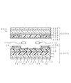
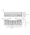
図35及び図36に従来の横電界方式のアクティブマトリクス型液晶表示装置の構造を示す。図35は、薄膜トランジスタ(以下、「TFT」と呼ぶ)が形成されるTFT基板100を液晶側から見た場合の平面図であり、図36は、図35のA−A’線に沿った本液晶表示装置の断面図である。
35 and 36 show the structure of a conventional lateral electric field type active matrix liquid crystal display device. FIG. 35 is a plan view of a
図36に示すように、本液晶表示装置は、TFT基板100と、TFT基板100に対向して配置されている対向基板200と、TFT基板100と対向基板200との間に形成されている液晶220の層と、から構成されている。
As shown in FIG. 36, the present liquid crystal display device includes a
TFT基板100は、ガラスからなる第一透明基板101と、第一透明基板101の上面(以下、液晶220に近い側の面を上面、液晶220から遠い側の面を下面と呼ぶ)上に形成された櫛歯状の共通電極127と、第一透明基板101の上面上に形成されたゲート配線105(図35参照)と、共通電極127を覆って第一透明基板101の上面上に形成された無機性の第一絶縁層間膜106と、第一絶縁層間膜106上に形成されたデータ線112と、第一絶縁層間膜106上に形成された櫛歯状の画素電極113と、データ線112及び画素電極113を覆って第一絶縁層間膜106上に形成された無機性の第二絶縁層間膜(パッシベーション膜)115と、第二絶縁層間膜115上に形成された配向膜120と、第一透明基板101の下面上に形成された偏光板130と、薄膜トランジスタと、から構成されている。
The
薄膜トランジスタは、共通電極127と同層に形成されたアイランド109と、データ線112と同層に形成されたドレイン電極110及びソース電極111と、上記のゲート配線105と、から構成されている。
The thin film transistor includes an
対向基板200は、ガラスからなる第二透明基板201と、第二透明基板201の上面上に部分的に形成されたブラックマトリクス層202と、第二透明基板201の上面上及びブラックマトリクス層202上に部分的に形成された色層203と、ブラックマトリクス層202及び色層203を覆って形成された平坦化層204と、平坦化層204上に形成された配向膜120と、第二透明基板201の下面上に形成された導電層205と、導電層205上に形成された偏光板210と、から構成されている。
The
TFT基板100と対向基板200との間にはスペーサー(図示せず)が挟み込まれており、液晶220の層を一定の厚さに保持している。
A spacer (not shown) is sandwiched between the
また、TFT基板100及び対向基板200の周囲には、液晶220の漏出を防止するためのシール材(図示せず)が設けられている。
In addition, a sealing material (not shown) for preventing leakage of the
図35及び図36に示した液晶表示装置においては、データ線112から発生する電気力線が画素電極113に入らないようにするため、データ線112の横に位置する共通電極127の面積を大きく取る必要があった。このため、図35及び図36に示した液晶表示装置は、開口率を大きくできないという問題点を有していた。
In the liquid crystal display device shown in FIGS. 35 and 36, the area of the
また、開口率を上げるため、共通電極127をデータ線112よりも液晶220に近い層で形成し、データ線112を共通電極127でシールドする方法が考えられる。この場合、シールド層としての共通電極127との結合容量を低減させるため、データ線112と共通電極127との間には有機系絶縁層間膜を形成する。
In order to increase the aperture ratio, a method in which the
有機系絶縁層間膜を形成する一般的な方法は、溶剤により液体化された感光性を有する有機系樹脂の液体(以下「フォトレジスト」と称する)を塗布装置でスリット塗布やスピン塗布し、所望の膜厚にする工程と、フォトレジストに対して、露光・現像・ベークからなるフォトリソグラフィー工程を施し、所望の有機膜パターン形状を得る工程と、からなる。 A general method for forming an organic insulating interlayer film is to apply a photosensitive organic resin liquid (hereinafter referred to as “photoresist”) liquefied with a solvent by slit coating or spin coating with a coating device. And a step of obtaining a desired organic film pattern shape by subjecting the photoresist to a photolithography step including exposure, development, and baking.
有機系絶縁層間膜に使用する材料としてはアクリル系樹脂が多く用いられる。 An acrylic resin is often used as a material for the organic insulating interlayer film.
アクリル系樹脂は、透明であるため、液晶表示装置における画素の部分に使用できるというメリットがあるが、同時に、以下のようなデメリットをも有していた。
(1)フォトリソグラフィー工程において、アクリル系樹脂は、一般的なノボラック系フォトレジスト塗布装置においてノボラック系樹脂と混在して使用することができない。このため、アクリル系樹脂専用の塗布装置を必要としていた。
(2)フォトリソグラフィー工程において、アクリル系樹脂用の現像液とノボラック系樹脂用の現像液とは異なるため、一般的なノボラック系フォトレジスト現像装置において、アクリル系樹脂をノボラック系樹脂と混在して現像することができない。このため、アクリル系樹脂専用の現像装置を必要としていた。
(3)アクリル系フォトレジストは常温保管できない。このため、冷蔵保管を行う必要があった。
(4)アクリル系フォトレジストは、常温では、経時変化が大きく、増粘し易い。
(5)アクリル系フォトレジストは固化し易いため、塗布装置のメンテナンス頻度が多くなることを避けられない。
(6)アクリル系フォトレジストは、ノボラック系フォトレジストに比較して、非常に高価である。
Since the acrylic resin is transparent, there is a merit that it can be used for a pixel portion in a liquid crystal display device, but at the same time, it has the following demerits.
(1) In the photolithography process, the acrylic resin cannot be used in combination with the novolak resin in a general novolak photoresist coating apparatus. For this reason, the application apparatus only for acrylic resin was required.
(2) In the photolithography process, an acrylic resin developer and a novolak resin developer are different from each other. Therefore, in a general novolak photoresist developing apparatus, an acrylic resin is mixed with a novolak resin. It cannot be developed. For this reason, a developing device dedicated to acrylic resin is required.
(3) Acrylic photoresist cannot be stored at room temperature. For this reason, it was necessary to perform refrigeration storage.
(4) Acrylic photoresist has a large change over time at room temperature, and tends to thicken.
(5) Since the acrylic photoresist is easily solidified, it is inevitable that the frequency of maintenance of the coating apparatus increases.
(6) Acrylic photoresists are very expensive compared to novolac photoresists.
これに対して、ノボラック系樹脂のデメリットは、ノボラック系樹脂は有色材料であるため、液晶表示装置の画素部に使用できない、という点のみである。 On the other hand, the demerit of the novolak resin is only that the novolac resin is a colored material and cannot be used for the pixel portion of the liquid crystal display device.
本発明は、上記のような問題点を解決するためになされたものであり、データ線から発生する電気力線が画素電極に進入することを防止し、開口率を大きくすることができる横電界方式のアクティブマトリクス型液晶表示装置及びその製造方法を提供することを目的とする。 The present invention has been made in order to solve the above-described problems, and prevents a line of electric force generated from a data line from entering a pixel electrode and can increase the aperture ratio. An object of the present invention is to provide an active matrix liquid crystal display device of the type and a method for manufacturing the same.
本発明は、さらに、有機系絶縁層間膜としてフォトリソグラフィー工程で一般的に使用されているノボラック系有機膜を使用することを可能にするため、ノボラック系有機膜のデメリットである有色性を回避することができる横電界方式のアクティブマトリクス型液晶表示装置を提供すること及びその製造方法を提供することを目的とする。 Furthermore, the present invention makes it possible to use a novolac organic film generally used in a photolithography process as the organic insulating interlayer film, thereby avoiding the chromaticity that is a disadvantage of the novolac organic film. It is an object of the present invention to provide a lateral electric field type active matrix liquid crystal display device and a manufacturing method thereof.
上記の目的を達成するため、薄膜トランジスタと、データ線と、画素電極と、共通電極とを備える第1基板と、第2基板と、前記第1と前記第2基板との間に挟まれる液晶とを備え、前記データ線を介して前記薄膜トランジスタに画像信号が印加され、前記画像信号を受けた前記画素電極と前記共通電極との間に電界が発生させ、前記電界により前記液晶が前記第1基板に平行な平面内で回転する液晶表示装置において、前記第1基板は、前記データ線を覆う無機絶縁膜と、前記データ線の上方において前記無機絶縁膜上に設けられた突起状の、ノボラック系樹脂からなる有機絶縁膜と、前記有機絶縁膜を完全に覆い、かつ、上方から見たときに前記データ線を覆うシールド共通電極と、を有し、前記第1基板上にはさらに前記薄膜トランジスタを選択するゲート配線が設けられ、前記ゲート配線及び前記データ線は前記第1基板の周辺でそれぞれゲート配線端子電極及びデータ線端子電極に接続され、前記ゲート配線端子電極及び前記データ線端子電極の上方には、前記突起状の有機絶縁膜と同時に形成される突起状のゲート端子有機絶縁膜及びデータ端子有機絶縁膜がそれぞれ形成され、 前記ゲート配線端子電極及び前記データ線端子電極はゲート端子有機絶縁膜及びデータ端子有機絶縁膜の上に前記共通電極と同時に形成されるゲート端子取出し電極及びデータ端子取出し電極に、ゲート配線端子下敷電極及びデータ配線端子下敷電極を介してそれぞれ電気的に接続されていることを特徴とする液晶表示装置を提供する。 To achieve the above object, a first substrate including a thin film transistor, a data line, a pixel electrode, and a common electrode, a second substrate, and a liquid crystal sandwiched between the first and second substrates, An image signal is applied to the thin film transistor through the data line, and an electric field is generated between the pixel electrode that has received the image signal and the common electrode, and the liquid crystal is applied to the first substrate by the electric field. In the liquid crystal display device rotating in a plane parallel to the first substrate, the first substrate includes an inorganic insulating film that covers the data line, and a protruding novolac system provided on the inorganic insulating film above the data line. an organic insulating film made of resin, completely cover the organic insulating film, and have a, and a shield common electrode covering the data line when viewed from above, the the first substrate further the thin film transitional A gate line for selecting the data, and the gate line and the data line are connected to the gate line terminal electrode and the data line terminal electrode around the first substrate, respectively, and the gate line terminal electrode and the data line terminal electrode A protrusion-shaped gate terminal organic insulating film and a data terminal organic insulating film formed at the same time as the protrusion-shaped organic insulating film are respectively formed above the gate wiring terminal electrode and the data line terminal electrode. Electrically connected to the gate terminal lead electrode and the data terminal lead electrode formed simultaneously with the common electrode on the organic insulating film and the data terminal organic insulating film through the gate wiring terminal underlay electrode and the data wiring terminal underlay electrode, respectively. It is to provide a liquid crystal display device according to claim Rukoto.
前記ゲート端子有機絶縁膜及び前記データ端子有機絶縁膜の下方には前記ゲート配線端子電極及び前記データ線端子電極と直接接触するゲート配線端子下敷電極及びデータ線端子下敷電極が設けられ、前記ゲート端子有機絶縁膜は前記ゲート端子取出し電極と前記ゲート配線端子下敷電極とに挟まれ、前記データ端子有機絶縁膜は前記データ端子取出し電極と前記データ線端子下敷電極との間に挟まれることが好ましい。 Below the gate terminal organic insulating film and the data terminal organic insulating film, a gate wiring terminal underlying electrode and a data line terminal underlying electrode that are in direct contact with the gate wiring terminal electrode and the data line terminal electrode are provided, and the gate terminal Preferably, the organic insulating film is sandwiched between the gate terminal lead electrode and the gate wiring terminal underlying electrode, and the data terminal organic insulating film is sandwiched between the data terminal leading electrode and the data line terminal underlying electrode.
本発明によれば、次のような効果を得ることができる。 According to the present invention, the following effects can be obtained.
第一に、共通電極はデータ線よりも液晶側に位置してデータ線を覆い、かつ、データ線上の無機絶縁膜上に設けられた突起状の有機絶縁膜を覆うシールド共通電極を有するので、シールド共通電極により、データ線からの電気力線を終端することができる。これにより、画素電極をデータ線の近傍に配置することができるようになり、開口率を向上させることができる。 First, since the common electrode has a shield common electrode located on the liquid crystal side of the data line and covering the data line, and covering the protruding organic insulating film provided on the inorganic insulating film on the data line, The electric lines of force from the data lines can be terminated by the shield common electrode. As a result, the pixel electrode can be arranged in the vicinity of the data line, and the aperture ratio can be improved.
第二に、ノボラック樹脂(及びその類似の物質)系有機膜をTFT基板の絶縁層間膜に適用することにより、データ線をシールドする共通電極とデータ線との間の寄生容量を低減させることができ、信号の遅延や消費電力を抑えることが可能となる。また、ゲート線上にノボラック有機層間膜を形成し、これを共通電極でシールドする場合には、ゲート線の寄生容量を低減することができ、ゲート線の遅延に伴うフリッカや画素書込みの面内不均一を抑制することができる。 Second, by applying a novolac resin (and similar material) organic film to the insulating interlayer film of the TFT substrate, the parasitic capacitance between the common electrode shielding the data line and the data line can be reduced. Thus, signal delay and power consumption can be suppressed. In addition, when a novolac organic interlayer film is formed on the gate line and is shielded by a common electrode, the parasitic capacitance of the gate line can be reduced, and flicker and pixel writing in-plane failure caused by delay of the gate line can be reduced. Uniformity can be suppressed.
第三に、アクリル系フォトレジストよりも安価なノボラック系フォトレジストを用いることにより、TFT基板を安価に製造することができる。 Third, a TFT substrate can be manufactured at a low cost by using a novolak photoresist that is less expensive than an acrylic photoresist.
第四に、TFT基板における層間絶縁膜としての有機膜の占有面積を極力小さくし、かつ、画素部に有機膜を配置しないため、画素部に配置する透明導電膜からなる櫛歯電極の膜質を向上させることが可能となり、櫛歯電極パターンを精度良く形成することが可能となる。 Fourth, in order to minimize the area occupied by the organic film as the interlayer insulating film on the TFT substrate and not to arrange the organic film in the pixel part, the film quality of the comb electrode made of the transparent conductive film arranged in the pixel part is It becomes possible to improve, and it becomes possible to form a comb-tooth electrode pattern accurately.
第五に、モリブデン(Mo)や銅(Cu)のような大気腐食性を有する金属からなる電極を有機絶縁膜で覆うことにより、大気暴露を防止し、電極の防食性能を大幅に向上させることが可能となる。 Fifth, by covering an electrode made of a metal having atmospheric corrosivity such as molybdenum (Mo) or copper (Cu) with an organic insulating film, exposure to the atmosphere is prevented and the anticorrosion performance of the electrode is greatly improved. Is possible.
第六に、モリブデン(Mo)や銅(Cu)のような大気腐食性を有する金属からなる電極を2層の透明導電膜で覆うことにより、大気暴露を防止し、電極の防食性能を大幅に向上させることが可能となる。 Sixth, by covering an electrode made of a metal having atmospheric corrosive properties such as molybdenum (Mo) and copper (Cu) with a two-layer transparent conductive film, exposure to the atmosphere is prevented and the anticorrosion performance of the electrode is greatly increased. It becomes possible to improve.
(第1の実施形態)
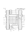
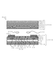
本発明の第1の実施形態に係る横電界方式のアクティブマトリクス型液晶表示装置500の構造を図1及び図2に示す。図1は、薄膜トランジスタが形成されるTFT基板100Aを液晶側から見た場合の平面図であり、図2は、図1のA−A’線に沿った本液晶表示装置500の断面図である。
(First embodiment)
The structure of a lateral electric field type active matrix liquid
図2に示すように、本液晶表示装置500は、TFT基板100Aと、TFT基板100Aに対向して配置されている対向基板200Aと、TFT基板100Aと対向基板200Aとの間に形成されている液晶220の層と、から構成されている。
As shown in FIG. 2, the present liquid
TFT基板100Aは、ガラスからなる第一透明基板1と、第一透明基板1の上面上に形成された無機性の第一絶縁層間膜6と、第一絶縁層間膜6上に形成されたデータ線12と、第一絶縁層間膜6上に形成された櫛歯状の画素電極13と、データ線12及び画素電極13を覆って第一絶縁層間膜6上に形成された無機性の第二絶縁層間膜(パッシベーション膜)15と、第二絶縁層間膜15上においてデータ線12の上方に形成されたノボラック系有機絶縁層21と、第二絶縁層間膜15上において画素電極13の間に形成された櫛歯状の共通電極27と、ノボラック系有機絶縁層21を覆って第二絶縁層間膜15上に形成された、共通電極27と同層のデータ線シールド26と、共通電極27、データ線シールド26及び第二絶縁層間膜15を覆う配向膜120と、第一透明基板101の下面上に形成された偏光板110と、第一透明基板1の上面上に形成されたゲート配線5(図1参照)と、薄膜トランジスタと、から構成されている。
The
薄膜トランジスタは、図1に示すように、アイランド9と、データ線12と同層に形成されたドレイン電極10及びソース電極11と、上記のゲート配線5と、から構成されている。
As shown in FIG. 1, the thin film transistor includes an
ゲート配線5は薄膜トランジスタを選択するために設けられており、ゲート配線5及びデータ線12はTFT基板100Aの外周部においてそれぞれゲート配線端子電極51(図26参照)及びデータ線端子電極53(図26参照)に接続されている。
The
対向基板200Aは、ガラスからなる第二透明基板201と、第二透明基板201の上面上に部分的に形成されたブラックマトリクス層202と、第二透明基板201の上面上及びブラックマトリクス層202上に部分的に形成された色層203と、ブラックマトリクス層202及び色層203を覆って形成された平坦化層204と、平坦化層204上に形成された配向膜120と、第二透明基板201の下面上に形成された導電層205と、導電層205上に形成された偏光板210と、から構成されている。
The
すなわち、対向基板200Aは、図36に示した対向基板200と同一の構造を有している。
That is, the
TFT基板100Aと対向基板200Aとの間にはスペーサー(図示せず)が挟み込まれており、液晶220の層を一定の厚さに保持している。
A spacer (not shown) is sandwiched between the
また、TFT基板100A及び対向基板200Aの周囲には、液晶220の漏出を防止するためのシール材(図示せず)が設けられている。
Further, a sealing material (not shown) for preventing the
本実施形態に係る液晶表示装置500においては、図2に示すように、データ線12の直上に、無機性の第二絶縁層間膜15及びノボラック系有機絶縁層21を介して、共通電極27と同層のデータ線シールド26を配置し、データ線シールド26でデータ線12を覆うようにしている。
In the liquid
このため、データ線シールド26により、データ線12から発生する電気力線が終端され、画素電極13にデータ線12からの電気力線が入ることを防止することができる。
Therefore, the electric lines of force generated from the
データ線12とその直上のデータ線シールド26との寄生容量が大きいと、信号の遅延や消費電力の増大と言った問題が出てくる。これらの問題を解決するため、ノボラック樹脂を主成分としたノボラック系有機絶縁層21の厚さを第二絶縁層間膜15の厚さよりも大きくすることにより、寄生容量を充分に小さくすることができる。
If the parasitic capacitance between the
データ線12の直上のデータ線シールド26により、データ線12からの電気力線を終端したことにより、画素電極13をデータ線12の近傍に配置することができるようになり、開口率を向上させることができる。
Since the electric lines of force from the
図1に示すように、画素電極13及び共通電極27とデータ線12は、液晶220の初期配向方向(ラビング方向)Rにおいて、相互に平行になるように液晶220をラビング方向に対して対称な2方向に回転させることができる。すなわち、本実施形態に係る液晶表示装置500はマルチドメインIPSを構成する。マルチドメインIPSにおいては、一の方向に回転したドメインと他の方向に回転したドメインとは互いに補償するため、視野角特性を向上させることができる。
As shown in FIG. 1, the
なお、対向基板200Aの一構成要素である平坦化膜204は、ブラックマトリクス層202及び色層203を覆うものであり、その膜厚は、1.5μm以上であることが望ましい。平坦化膜204の膜厚を1.5μm以上とすることにより、ブラックマトリクス層202とノボラック系有機絶縁層21を覆うデータ線シールド26との間隔を十分広くとることができるため、ブラックマトリクス層202による電界の阻害がなくなり、良好な表示を得ることができる。
Note that the
また、ブラックマトリクス層202の抵抗率は1E9Ω・cm以上であることが望ましい。これにより、ブラックマトリクス層202による電界の阻害を抑制することができ、良好な表示を得ることができる。
The resistivity of the
また、データ線12に対向する位置においては、ブラックマトリクス層202を形成することに代えて、この部分を相異なる2色以上の色層の積層膜を形成することもできる。この場合においても、2色以上の色層の積層膜は、十分に余分な光を遮断する作用を有すると同時に、この積層部分の抵抗は非常に大きいので、抵抗率の大きなブラックマトリクス層202を形成する場合に比べて、さらに、この部分での電界の阻害による影響を受けることが少なくなり、良好な表示性能を得ることができる。
In addition, at the position facing the
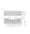
図3(a)はデータ線12の形状を示す部分的な平面図であり、図3(b)は、図3(a)の点線で囲んだ四角形の領域Sの拡大図である。
FIG. 3A is a partial plan view showing the shape of the
データ線12は、図3(b)に示すように、ジグザグ(櫛歯状)に屈曲する形状を有している。データ線12を画素電極13及び共通電極27と平行となるようにジグザグに屈曲させることにより、画素表示部の光透過領域を効率よく形成することができる。
As shown in FIG. 3B, the
図3(c)は、データ線12の形状の他の例を示す部分的な平面図である。
FIG. 3C is a partial plan view showing another example of the shape of the
データ線12は、図3(c)に示すように、ラビング方向Rと平行な直線部分12aをラビング方向Rと平行に一定間隔でジグザグに配置し、それらの直線部分12aを傾斜した傾斜部分12bで接合するように形成することもできる。このようにしても、光利用効率を大きく落とすことはない。 As shown in FIG. 3C, the data lines 12 are arranged in a zigzag manner with linear portions 12a parallel to the rubbing direction R at regular intervals parallel to the rubbing direction R, and the inclined portions 12b inclined by the linear portions 12a. It can also be formed so as to be joined. Even if it does in this way, light utilization efficiency will not be reduced significantly.
さらに、データ線12に沿うように形成するノボラック系有機絶縁層21のパターンは、データ線12がラビング方向Rに平行に延在する直線部分12aにおいては、ラビング方向Rに平行なパターンとして形成することができる。このようにすると、ラビングする際に、ラビング布がノボラック系有機絶縁層21のパターンから受ける影響を小さくすることができるため、ノボラック系有機絶縁層21のパターンの近傍の配向膜120の配向をより均一に行うことができる。これにより、液晶220の配向方向が安定し、表示コントラストを向上させることができる。
Further, the pattern of the novolac organic insulating
(第2の実施形態)
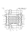
本発明の第2の実施形態に係る横電界方式のアクティブマトリクス型液晶表示装置510の構造を図4及び図5に示す。図4は、薄膜トランジスタが形成されるTFT基板100Aを液晶側から見た場合の平面図であり、図5は、図4のA−A’線に沿った本液晶表示装置510の断面図である。
(Second Embodiment)
The structure of a lateral electric field type active matrix liquid
第1の実施形態に係る液晶表示装置500においては、画素電極13及び共通電極27とデータ線12は、ラビング方向Rに対して平行になるようにジグザグ(櫛歯状)に屈曲している。これにより、2方向に横電界を発生させ、この電界により、液晶220をラビング方向Rに対して対称な2方向に回転させる。一の方向に回転したドメインと他の方向に回転したドンメインは互いに補償するため、視野角特性を向上させることができる。
In the liquid
すなわち、図1及び図2に示した第1の実施形態に係る液晶表示装置500はマルチドメインIPS構造を有している。
That is, the liquid
これに対して、本実施形態に係る液晶表示装置510においては、図4と図1との比較から明らかであるように、図1及び図2に示した第1の実施形態に係る液晶表示装置500とは異なり、データ線12、画素電極13及び共通電極27(データ線シールド26を含む)がゲート配線5に対して垂直な方向に、屈曲することなく、直線状に延びている。
On the other hand, in the liquid
すなわち、本実施形態に係る液晶表示装置510はシングルドメインIPS構造を有している。このように、本発明は、マルチドメインIPSのみならず、シングルドメインIPSに対しても適用することができる。
That is, the liquid
データ配線5上の第二無機絶縁層間膜15上に設けられたノボラック系有機絶縁層21及びこれを覆うデータ線シールド(共通電極)26は、図4に示すように、画素部のデータ線12の上を全て覆うように形成することもできる。このように、データ線12をノボラック系有機絶縁層21及びデータ線シールド(共通電極)26で覆うことにより、例えば、データ線シールド(共通電極)26のパターンを形成する際のエッチング液(エッチャント)がデータ線12上の第二無機絶縁層間膜15のピンホールに染み込んで、データ線12を断線させるといった問題を抑制することができる。
As shown in FIG. 4, the novolac organic insulating
(第3の実施形態)
本発明の第3の実施形態に係る横電界方式のアクティブマトリクス型液晶表示装置520の構造を図6及び図7に示す。図6は、薄膜トランジスタが形成されるTFT基板100Aを液晶側から見た場合の平面図であり、図7は、図6のA−A’線に沿った本液晶表示装置520の断面図である。
(Third embodiment)
The structure of a horizontal electric field type active matrix liquid
本実施形態に係る液晶表示装置520は、図1及び図2に示した第1の実施形態に係る液晶表示装置500と比較して、画素電極が2層に分けて形成されている点が異なっている。すなわち、本実施形態に係る液晶表示装置520においては、画素電極は上層画素電極313と下層画素電極413とから構成されている。
The liquid
第1の実施形態に係る液晶表示装置500においては、画素電極13は、第一絶縁層間膜6上に形成されているのに対して、本実施形態に係る液晶表示装置520においては、下層画素電極413は第一絶縁層間膜6上に形成されており、上層画素電極313は、第二絶縁層間膜(パッシベーション膜)15上に、すなわち、最上層に形成されている。上層画素電極313が形成される位置を除いて、本実施形態に係る液晶表示装置520は第1の実施形態に係る液晶表示装置500と同一の構造を有している。
In the liquid
本実施形態に係る液晶表示装置520によっても、第1の実施形態に係る液晶表示装置500と同様の効果を得ることができる。
Also with the liquid
第2の実施形態に係る液晶表示装置510と同様に、本実施形態に係る液晶表示装置520においても、データ配線5上の第二無機絶縁層間膜15上に設けられたノボラック系有機絶縁層21及びこれを覆うデータ線シールド(共通電極)26は、図6に示すように、画素部のデータ線12の上を全て覆うように形成することもできる。このように、データ線12をノボラック系有機絶縁層21及びデータ線シールド(共通電極)26で覆うことにより、例えば、データ線シールド(共通電極)26のパターンを形成する際のエッチング液(エッチャント)がデータ線12上の第二無機絶縁層間膜15のピンホールに染み込んで、データ線12を断線させるといった問題を抑制することができる。
Similar to the liquid
(第4の実施形態)
本発明の第4の実施形態に係る横電界方式のアクティブマトリクス型液晶表示装置530の構造を図8及び図9に示す。図8は、薄膜トランジスタが形成されるTFT基板100Aを液晶側から見た場合の平面図であり、図9は、図8のA−A’線に沿った本液晶表示装置530の断面図である。
(Fourth embodiment)
The structure of a lateral electric field type active matrix liquid
本実施形態に係る液晶表示装置530においては、第3の実施形態に係る液晶表示装置520と同様に、画素電極は上層画素電極313と下層画素電極413とから構成されており、下層画素電極413第一絶縁層間膜6上に形成され、上層画素電極313は、第二絶縁層間膜(パッシベーション膜)15上に、すなわち、最上層に形成されている。上層画素電極313が形成される位置を除いて、本実施形態に係る液晶表示装置530は第1の実施形態に係る液晶表示装置500と同一の構造を有している。
In the liquid
本実施形態に係る液晶表示装置530によっても、第1の実施形態に係る液晶表示装置500と同様の効果を得ることができる。
Also by the liquid
本実施形態に係る液晶表示装置530においては、図8に示すように、データ線12を覆う第二無機絶縁層間膜15上に設けられたノボラック系有機絶縁層21は、画素部のデータ線12の上を全て覆うように形成し、かつ、ノボラック系有機絶縁層21を覆うデータ線シールド(共通電極)26は表示に関係のある領域にだけ限定して形成することもできる。
In the liquid
ノボラック系有機絶縁層21及びデータ線シールド(共通電極)26をこのように形成することにより、データ線12がノボラック系有機絶縁層21で覆われているため、データ線シールド(共通電極)26のパターンを形成する際のエッチング液(エッチャント)がデータ線12上の第二無機絶縁層間膜15のピンホールに染み込んで、データ線12を断線させるといった問題を抑制することができる。
By forming the novolac organic insulating
さらに、データ線シールド(共通電極)26は必要な部分にのみ形成されているため、データ線12とデータ線シールド(共通電極)26との間の容量の増加を防止することができる。
Furthermore, since the data line shield (common electrode) 26 is formed only in a necessary portion, an increase in capacitance between the
(第5の実施形態)
本発明の第5の実施形態に係る横電界方式のアクティブマトリクス型液晶表示装置540の構造を図10及び図11に示す。図10は、薄膜トランジスタが形成されるTFT基板100Aを液晶側から見た場合の平面図であり、図11は、図10のA−A’線に沿った本液晶表示装置540の断面図である。
(Fifth embodiment)
The structure of a lateral electric field type active matrix liquid
本実施形態に係る液晶表示装置540においては、第3の実施形態に係る液晶表示装置520と同様に、画素電極は上層画素電極313と下層画素電極413とから構成されており、下層画素電極413第一絶縁層間膜6上に形成され、上層画素電極313は、第二絶縁層間膜(パッシベーション膜)15上に、すなわち、最上層に形成されている。上層画素電極313が形成される位置を除いて、本実施形態に係る液晶表示装置540は第1の実施形態に係る液晶表示装置500と同一の構造を有している。
In the liquid
本実施形態に係る液晶表示装置540によっても、第1の実施形態に係る液晶表示装置500と同様の効果を得ることができる。
Also by the liquid
本実施形態に係る液晶表示装置540においては、図10に示すように、データ線12を覆う第二無機絶縁層間膜15上に設けられたノボラック系有機絶縁層21及びこれを覆うデータ線シールド(共通電極)26は、表示に関係のある領域だけに限定して形成し、データ線12とゲート配線5とが交差する領域の近傍には、ノボラック系有機絶縁層21及びこれを覆うデータ線シールド(共通電極)26を設けないようにすることもできる。
In the liquid
図1に示した第1の実施形態に係る液晶表示装置500、図4に示した第2の実施形態に係る液晶表示装置510、図6に示した第3の実施形態に係る液晶表示装置520、図8に示した第4の実施形態に係る液晶表示装置530の場合には、ノボラック系有機絶縁層21が全データ線12に対して壁のように存在するため、パネル内に液晶220を注入するような場合に、液晶220が入りにくいといった問題点がある。これに対して、本実施形態に係る液晶表示装置540においては、ノボラック系有機絶縁層21のパターンに隙間があるため、このような問題が軽減されるという効果がある。
The liquid
(第6の実施形態)
本発明の第6の実施形態に係る横電界方式のアクティブマトリクス型液晶表示装置550の構造を図12及び図13に示す。図12は、薄膜トランジスタが形成されるTFT基板100Aを液晶側から見た場合の平面図であり、図13は、図12のA−A’線に沿った本液晶表示装置550の断面図である。
(Sixth embodiment)
The structure of a lateral electric field type active matrix liquid
図6及び図7に示した第3の実施形態に係る液晶表示装置520はマルチドメインIPS構造を有している。
The liquid
これに対して、本実施形態に係る液晶表示装置550においては、図12と図6との比較から明らかであるように、図6及び図7に示した第3の実施形態に係る液晶表示装置520とは異なり、データ線12、画素電極13及び共通電極27(データ線シールド26を含む)がゲート配線5に対して垂直な方向に、屈曲することなく、直線状に延びている。
On the other hand, in the liquid
すなわち、本実施形態に係る液晶表示装置550はシングルドメインIPS構造を有している。これ以外の構造は第3の実施形態に係る液晶表示装置520と同様である。
That is, the liquid
このように、第3の実施形態に係る液晶表示装置520は、マルチドメインIPSとしてのみならず、シングルドメインIPSとして構成することも可能である。同様に、第4の実施形態に係る液晶表示装置530及び第5の実施形態に係る液晶表示装置540も、マルチドメインIPSとしてのみならず、シングルドメインIPSとして構成することも可能である。
As described above, the liquid
(第7の実施形態)
図14、図15及び図16は、図1及び図2に示した第1の実施形態に係る液晶表示装置500におけるTFT基板100Aの製造工程を順に示す同TFT基板の断面図であり、図1のA−A’線に沿った断面(画素部)の他に、TFT素子、共通電極配線コンタクト部、データ線端子部、ゲート配線端子(共通配線端子)部、ゲート配線の各断面を含む断面図である。以下、第7の実施形態として、第1の実施形態に係る液晶表示装置500の製造方法を図14乃至図16を参照して製造工程順に説明する。
(Seventh embodiment)
14, FIG. 15 and FIG. 16 are cross-sectional views of the TFT substrate sequentially showing the manufacturing process of the
先ず、図14(a)に示すように、第一透明基板1上に、スパッタ法により、モリブデン(Mo)を400nmの厚さで成膜する。次いで、モリブデン膜に対してフォトリソグラフィーを行い、ゲート電極2、共通電極配線3、ゲート端子電極4及びゲート配線5を形成する。
First, as shown in FIG. 14A, a molybdenum (Mo) film is formed to a thickness of 400 nm on the first
ここで、配線材料は、Mo系以外でも可能であり、例えば、Cr系、Al系、Cu系、Ag系、Ti系、W系の金属であっても良い。 Here, the wiring material may be other than Mo-based, and may be, for example, Cr-based, Al-based, Cu-based, Ag-based, Ti-based, or W-based metal.
次いで、図14(b)に示すように、ゲート電極2、共通電極配線3、ゲート端子電極4及びゲート配線5を覆って第一透明基板1上に膜厚100nmの二酸化シリコン(SiO2)膜をCVD法で成膜し、この二酸化シリコン(SiO2)膜上に、シリコン窒化膜(ゲート−SiNx)を300nm厚さでCVD法により成膜する。これらの二酸化シリコン(SiO2)膜及びシリコン窒化膜が第1絶縁層間膜6を形成する。
Next, as shown in FIG. 14B, a silicon dioxide (SiO 2 ) film having a thickness of 100 nm is formed on the first
さらに、シリコン窒化膜上に、アモルファスシリコン膜(a−Si)7を215nm、n+型アモルファスシリコン(a−Si)膜8を50nmの厚さで順にCVD法で成膜する。
Further, on the silicon nitride film, an amorphous silicon film (a-Si) 7 is formed in a thickness of 215 nm and an n + type amorphous silicon (a-Si)
次に、フォトリソグラフィーを行い、a−Siドライエッチングにより、不要なa−Siを除去して、図14(b)に示すように、アイランド9を形成する。
Next, photolithography is performed, and unnecessary a-Si is removed by a-Si dry etching to form
その上にスパッタ法で再びモリブデン(Mo)を210nmの厚さで成膜し、モリブデン膜に対してフォトリソグラフィーを行い、図14(c)に示すように、薄膜トランジスタのドレイン電極10及びソース電極11を形成する。
Then, a molybdenum (Mo) film is again formed to a thickness of 210 nm by sputtering, and photolithography is performed on the molybdenum film. As shown in FIG. 14C, the
ドレイン電極10及びソース電極11の形成と同時に、データ線12、画素電極13及びデータ線端子電極14を形成する。
Simultaneously with the formation of the
ドレイン電極10、ソース電極11、データ線12、画素電極13及びデータ線端子電極14の配線材料としては、Mo系以外の金属を選択することもできる。例えば、Cr系、Al系、Cu系、Ag系、Ti系、W系の金属であっても良い。
As a wiring material for the
続いて、薄膜トランジスタのバックチャネル部の余分なn+型アモルファスシリコン(a−Si)膜8をドライエッチでエッチングし、除去する(図14(c))。
Subsequently, the excess n + -type amorphous silicon (a-Si)
その上に膜厚300nmの窒化シリコン(SiNx)からなるパッシベーション膜15をCVD法により成膜し、270℃程度の熱処理をする。この熱処理は、ノボラック系有機膜の焼成工程で代用することにより、省くこともできる。
A
その後、フォトリソグラフィー及びドライエッチングを行い、あるいは、バッファードフッ酸によるエッチング及びドライエッチングからなるウェット及びドライプロセスを用いて、パッシベーション膜15及び第1絶縁層間膜6(データ線端子電極14上はパッシベーション膜15のみ)を開口し、図15(a)に示すように、コンタクトホール16、17、18を形成する。コンタクトホール16は共通電極配線3に、コンタクトホール17はデータ線端子電極14に、コンタクトホール18はゲート端子電極4にそれぞれ達している。
Thereafter, the
このようなコンタクトホール16、17、18を形成することにより、その後のノボラック系有機絶縁層21のパターン形成時のレジスト剥離液によるダメージを避けることができる。
By forming such contact holes 16, 17, 18, it is possible to avoid damage due to the resist stripping solution during the subsequent pattern formation of the novolac organic insulating
次いで、パッシベーション膜15上に第1回目の膜厚40nmのITOをスパッタ法で成膜し、フォトリソグラフィーを行い、図15(b)に示すように、層間コンタクト19を形成する。
Next, a first ITO film having a thickness of 40 nm is formed on the
ここまでの工程により、逆スタガ型TFTが完成する。 The reverse stagger type TFT is completed through the steps so far.
次いで、図15(c)に示すように、パッシベーション膜15及び層間コンタクト19を覆って、焼成後の膜厚が2μm程度になるように感光性耐熱性ノボラックレジスト20を塗布する。
Next, as shown in FIG. 15C, a photosensitive heat-resistant novolac resist 20 is applied so as to cover the
次いで、感光性耐熱性ノボラックレジスト20に対してフォトリソグラフィーを行い、データ線12、共通電極配線3、データ線端子電極14、ゲート端子電極4及びゲート配線5上にのみノボラック系有機絶縁層21、22、23、24、25を残し、他のノボラックレジスト20は除去する。
Next, photolithography is performed on the photosensitive heat-resistant novolak resist 20, and the novolac organic insulating
その後、140℃での熱処理を行い、ノボラック系有機絶縁層21、22、23、24、25をメルトさせ、図16(a)に示すように、ノボラック系有機絶縁層21、22、23、24、25の断面形状を逆U字状にする。その後、焼成炉に入れ、240℃で加熱し、焼き締める。
Thereafter, heat treatment at 140 ° C. is performed to melt the novolac organic insulating
次いで、図16(a)に示した基板上に第2回目の膜厚40nmのITOをスパッタ法で成膜し、このITO膜に対してフォトリソグラフィーを行い、図16(b)に示すように、データ線シールド26、櫛歯状の共通電極27、共通電極用ITO28、データ線端子用ITO29及びゲート配線端子・共通配線端子用ITO30を形成する。
Next, a second ITO film having a thickness of 40 nm is formed on the substrate shown in FIG. 16A by sputtering, and photolithography is performed on the ITO film, as shown in FIG. 16B. The
共通電極配線3及びデータ線端子電極14、ゲート端子電極4を構成する大気腐食性金属であるモリブデン(Mo)は層間コンタクト(第1のITO)19と共通電極用ITO(第2のITO)28の2層で覆われているため、モリブデン(Mo)の防食性能が向上する。
Molybdenum (Mo), which is an atmospheric corrosive metal constituting the
ゲート端子電極4の一例の平面図を図17(a)に、データ線端子電極14の一例の平面図を図17(b)に示す。
A plan view of an example of the
大気腐食性金属であるモリブデン(Mo)からなるゲート端子電極4は、パッシベーション膜(SiNx)15及び第1絶縁層間膜6に形成されたコンタクトホール18の内壁を覆っている層間コンタクト(第1のITO)19に接続されている。更に、ゲート配線端子・共通配線端子用ITO(第2のITO)30で層間コンタクト(第1のITO)19を覆うことにより、ゲート端子電極4の耐腐食性をより向上させることができる。
The
図18は、ノボラック系有機絶縁層25(または21)と、ノボラック系有機絶縁層25を覆うゲート配線シールド31(またはデータ線シールド26)と、ゲート配線5(またはデータ線12)との位置関係を示す断面図である。
FIG. 18 shows the positional relationship between the novolac organic insulating layer 25 (or 21), the gate wiring shield 31 (or data line shield 26) covering the novolac organic insulating
図18に示すように、ノボラック系有機絶縁層25が水平方向においてゲート配線5からはみ出している量は0.5μm乃至4.0μmの範囲に設定されている。同様に、ノボラック系有機絶縁層21が水平方向においてデータ線12からはみ出している量は0.5μm乃至4.0μmの範囲に設定されている。
As shown in FIG. 18, the amount of the novolac organic insulating
また、ゲート配線シールド31(またはデータ線シールド26)が水平方向においてノボラック系有機絶縁層25(または21)からはみ出している量は0μm乃至3.0μmの範囲に設定されている。この範囲内においてゲート配線シールド31(またはデータ線シールド26)を形成することにより、データ線12とデータ線シールド26との寄生容量、ゲート配線5とゲート配線シールド31との寄生容量のバラツキを小さくすることができ、データ線12(または、データ線12及びゲート配線5の両方)からの漏れ電界のシールド性も充分となる。
The amount of the gate wiring shield 31 (or the data line shield 26) protruding from the novolac organic insulating layer 25 (or 21) in the horizontal direction is set in the range of 0 μm to 3.0 μm. By forming the gate wiring shield 31 (or the data line shield 26) within this range, the parasitic capacitance between the
また、ノボラック系有機絶縁層25(又は21)がゲート配線シールド(ITOシールド)31(又はデータ線シールド26)で完全に覆われているため、ノボラック系有機絶縁層25、21がITOエッチャントやレジスト剥離液に直接暴露されることがなくなるので、ノボラック系有機絶縁層25、21の薬液による劣化を防止することができる。
Further, since the novolac organic insulating layer 25 (or 21) is completely covered with the gate wiring shield (ITO shield) 31 (or the data line shield 26), the novolac organic insulating
耐熱性ノボラック系有機絶縁層の典型的な比誘電率は4.2程度であり、SiNx膜の3分の2程度と小さいため、SiNx膜よりも薄い膜厚で寄生容量を低減することができるという効果もある。 The typical relative dielectric constant of the heat-resistant novolac organic insulating layer is about 4.2, which is as small as about two-thirds of the SiNx film, so that the parasitic capacitance can be reduced with a film thickness thinner than that of the SiNx film. There is also an effect.
また、データ線12の直上に、無機性の第二絶縁層間膜15及びノボラック系有機絶縁層21を介して、共通電極を構成するデータ線シールド(ITO)26を配置し、データ線シールド(ITO)26でデータ線12を覆うことにより、データ線12からの電気力線を終端することができる。これにより、画素電極13にデータ線12からの電気力線が進入することを防止することができる。
Further, a data line shield (ITO) 26 constituting a common electrode is disposed directly above the
データ線12とその直上のデータ線シールド26との寄生容量が大きいと、信号の遅延や消費電力の増大などの問題が生じるが、ノボラック樹脂を主成分としたノボラック系有機絶縁層21を第二絶縁層間膜15に比較して厚くし、寄生容量を充分に小さくすることにより、この問題を解決することができる。
If the parasitic capacitance between the
データ線12の直上のデータ線シールド26でデータ線12からの電気力線を終端することにより、画素電極13をデータ線12の近傍に配置することができるようになり、開口率を向上させることができる。
Terminating the electric lines of force from the
(第8の実施形態)
本発明の第8の実施形態に係る横電界方式のアクティブマトリクス型液晶表示装置560の構造を図19及び図20に示す。図19は、薄膜トランジスタが形成されるTFT基板100Aを液晶側から見た場合の平面図であり、図20は、図19のA−A’線に沿った本液晶表示装置560の断面図である。
(Eighth embodiment)
The structure of a lateral electric field type active matrix liquid
本実施形態に係る液晶表示装置560は、図10及び図11に示した第5の実施形態に係る液晶表示装置540の変形例に相当する。
The liquid
上記のように、図10及び図11に示した第5の実施形態に係る液晶表示装置540においては、液晶注入効率を上げるために、ゲート配線5とデータ線12との交差領域を除いたデータ線12上のみにノボラック系有機絶縁層21を残している。
As described above, in the liquid
このようにノボラック系有機絶縁層21を形成した場合、データ線12とデータ線シールド(共通電極)26との間の容量増加を避けるため、ゲート配線5とデータ線12の交差領域上においてはデータ線12上にデータ線シールド(共通電極)26を配置することができない。従って、第5の実施形態に係る液晶表示装置540においては、ゲート配線(走査ライン)5ごとにデータ線シールド(共通電極)26は独立している。
When the novolac organic insulating
これに対して、本実施形態に係る液晶表示装置560においては、ノボラック系有機絶縁層21を残していないゲート配線5とデータ線12との交差領域において、データ線12を避けて、上下の画素のデータ線シールド(共通電極)26を相互に接続している。すなわち、データ線シールド(共通電極)26をデータ線12と重ならないようにデータ線12上を通過させ、上下の画素のデータ線シールド(共通電極)26をこれと同じ導電層で相互に接続している。この点以外の構造は第5の実施形態に係る液晶表示装置540と同様である。
On the other hand, in the liquid
なお、共通電極27は画素電極313に重ならないように配置されている。
The
本実施形態に係る液晶表示装置560は、以上のような構造を有することにより、以下の効果を奏することができる。
The liquid
例えば、対角18インチ以上のような大型で高精細のパネルにおいては、共通電極配線3の配線抵抗Rcと各画素の画素電極13と共通電極27の間の容量Cpとによる時定数が大きくなることが避けられない。この結果として、あるゲート配線5(走査線)によって書きこみが制御されている画素群においては、ゲート配線5(走査線)の電圧の立ち下がりにおいて、画素電極13の電位が、ゲート配線5(走査線)との容量結合(主として、トランジスタの寄生容量)により、一斉に電圧降下を起こす。このとき、画素電極13と共通電極27との間の容量Cpにより、共通電極配線3の電位も降下し、配線抵抗Rcと容量Cpとの積に比例する時定数に応じて、共通電極配線3の遅延が生じてしまう。
For example, in a large, high-definition panel having a diagonal size of 18 inches or more, the time constant due to the wiring resistance Rc of the
このように共通電極配線3に遅延が生じると、画素電極13の電位がより大きな電圧降下を瞬間的に引き起こす。この結果、ゲート配線5(走査線)の電圧の立ち下がりにおいて、データ線12の電位と画素電極13の電位との差が大きくなる。
When a delay occurs in the
一方、ゲート配線5(走査線)にも遅延が生じるので、データ線12の電位と画素電極13の電位との間に差分が生じると、ゲート配線5(走査線)がオフになり切らない間に、データ線12から画素電極13への電荷の流れ(画素電極13への再書込み)が生じる。共通電極配線3の遅延による共通電極27の電位の下方への変動により、この再書き込み量が大きくなる。
On the other hand, since a delay also occurs in the gate wiring 5 (scanning line), if a difference occurs between the potential of the
この結果、共通電極配線3の遅延が一定時間後に設定値まで回復した状態において、画素電極13の電位がより高くなることになる。従って、共通電極27の電位がより高い状態において、画素電極13の平均電位と共通電極27の電位とが等しくなり、両者の間にDC電位を生じなくなり、フリッカや残像を抑制することができる。
As a result, the potential of the
一例として作成した19型SXGAパネルのゲート配線5(走査線)の方向において、面内の画素電極13の電位の平均値をプロットした結果(面内フィードスルー電圧差)を図21(a)に示す。
FIG. 21A shows the result (in-plane feedthrough voltage difference) of plotting the average value of the potentials of the in-
すなわち、図21(a)に示す面内フィードスルー電圧差は、フィードスルー電圧の面内ばらつきを、正負フレームの画素電圧平均値の面内分布として表したものである。なお、図21(b)は、19型SXGAパネルにおいて、フィードスルー電圧の面内ポイントを示す概略図である。 That is, the in-plane feedthrough voltage difference shown in FIG. 21A represents the in-plane variation of the feedthrough voltage as an in-plane distribution of pixel voltage average values of positive and negative frames. FIG. 21B is a schematic diagram showing in-plane points of the feedthrough voltage in the 19-inch SXGA panel.
図10及び図11に示した第5の実施形態に係る液晶表示装置540のように上下のデータ線シールド(共通電極)26を接続しない場合は、図中の「上下接続なし」と記したプロットのように、画素電極13の平均電位がゲート配線5(走査線)に沿って面内で大きく変動し、面内で一様にフリッカを抑制することが困難となる。
When the upper and lower data line shields (common electrodes) 26 are not connected as in the liquid
これに対して、本実施形態に係る液晶表示装置560のように、上下の画素のデータ線シールド(共通電極)26を相互に接続すると、データ線シールド(共通電極)26はゲート配線5(走査線)の電位の変動の生じない画素につながる共通電極配線3に接続されることとなり、その結果、上述のような共通電極配線3の電位の下方への変動が顕著に抑制されることとなる。
On the other hand, when the data line shields (common electrodes) 26 of the upper and lower pixels are connected to each other as in the liquid
その結果、上下の画素のデータ線シールド(共通電極)26を接続する際の抵抗を図21(a)のように変化させて、画素電極13の平均電位を評価したところ、接続抵抗が750kΩ以下である場合に、ゲート配線(走査線)5の方向における画素電極13の平均電位の変動を顕著に抑制することができた。
As a result, the resistance at the time of connecting the data line shields (common electrodes) 26 of the upper and lower pixels was changed as shown in FIG. 21A, and the average potential of the
すなわち、図21(a)からは、データ線シールド(共通電極)26をマトリクス化することにより、面内のフィードスルー電圧の面内ばらつきを低減させ、また、データ線シールド(共通電極)26の接続抵抗が750kΩ/画素以下の場合に、大きな効果が得られることが分かる。 That is, from FIG. 21A, by forming the data line shield (common electrode) 26 in a matrix, the in-plane variation of the in-plane feedthrough voltage is reduced, and the data line shield (common electrode) 26 It can be seen that a great effect is obtained when the connection resistance is 750 kΩ / pixel or less.
また、このような共通電極27の遅延を抑制することにより、ゲート配線(走査線)5がオンしている期間中の共通電極配線3の遅延をも抑制することができ、横クロストークをも抑制することができる。
Further, by suppressing the delay of the
また、上下の画素のデータ線シールド(共通電極)26を接続する際に、ノボラック系有機絶縁層21が形成されていないゲート配線5とデータ線12との交差領域付近において、データ線12と重ならないようにデータ線シールド(共通電極)26を相互に接続しているため、データ線12とデータ線シールド(共通電極)26との間の容量が増加することがない。このため、データ線12の遅延や共通電極配線3の遅延が増大することもなく、良好な品質を維持することができる。
Further, when connecting the data line shields (common electrodes) 26 of the upper and lower pixels, the data lines 12 are overlapped with the data lines 12 in the vicinity of the intersection region of the
(第9の実施形態)
本発明の第9の実施形態に係る横電界方式のアクティブマトリクス型液晶表示装置570の構造を図22及び図23に示す。図22は、薄膜トランジスタが形成されるTFT基板100Aを液晶側から見た場合の平面図であり、図23は、図22のA−A’線に沿った本液晶表示装置570の断面図である。
(Ninth embodiment)
The structure of a lateral electric field type active matrix liquid
本実施形態に係る液晶表示装置570においては、第8の実施形態に係る液晶表示装置560と同様に、隣接する上下の画素のデータ線シールド(共通電極)26を相互に接続しているとともに、隣接する上下の画素のデータ線シールド(共通電極)26どうしを接続する領域を広げて、ゲート配線5上を広い範囲でデータ線シールド(共通電極)26の接続領域によって覆っている。この点以外の構造は第5の実施形態に係る液晶表示装置540と同様である。
In the liquid
以上のような構造を有する第9の実施形態に係る液晶表示装置570によれば、以下のような効果を奏することができる。
According to the liquid
本実施形態に係る液晶表示装置570においては、第8の実施形態に係る液晶表示装置560と同様に、隣接する上下の画素のデータ線シールド(共通電極)26を相互に接続していることに加えて、ゲート配線5上をデータ線シールド(共通電極)26と等電位の接続領域で覆っている。
In the liquid
これにより、共通電極配線3の遅延を低減させることができることに加えて、ゲート配線5とブラックマトリクス層202との間の容量結合を低減させることができ、この結果として、ブラックマトリクス層202の電位は、ゲート配線5のオフ時のマイナス電位により、マイナス電位にバイアスされることを抑制することができる。このため、ブラックマトリクス層202の電位のデータ線シールド(共通電極)26の電位からの変動に伴う残像等の問題を抑制することが可能となる。
Thereby, in addition to being able to reduce the delay of the
実験的には、他の導電層で覆われていないゲート配線5の6割以上をデータ線シールド(共通電極)26と等電位の接続領域で覆うことにより、顕著な効果が得られた。
Experimentally, a remarkable effect was obtained by covering 60% or more of the
また、本実施形態に係る液晶表示装置570においても、ノボラック系有機絶縁層21が形成されていないゲート配線5とデータ線12との交差部付近において、データ線12と重ならないようにデータ線シールド(共通電極)26を接続しているため、データ線12とデータ線シールド(共通電極)26との間の容量の増加を防止することができる。このため、データ線12の遅延や共通電極配線3の遅延が増大することもなく、良好な品質を維持することができる。
Also in the liquid
以上の第1乃至第6、第8及び第9の実施形態に係る液晶表示装置500、510、520、530、540、550、560、570、においては、ノボラック系有機絶縁層21を絶縁層間膜として用いている。
In the liquid
図24はノボラック系有機絶縁膜を形成する方法のフローチャートであり、図25はアクリル系有機絶縁膜を形成する方法のフローチャートである。以下、図24及び図25を参照して、ノボラック系有機絶縁層21を絶縁層間膜として用いることによる利点を、アクリル系有機膜を絶縁層間膜として用いた場合と比較して、説明する。
FIG. 24 is a flowchart of a method for forming a novolac organic insulating film, and FIG. 25 is a flowchart of a method for forming an acrylic organic insulating film. Hereinafter, the advantage of using the novolac organic insulating
図24及び図25に示すように、ノボラック系有機膜を形成する方法及びアクリル系有機膜を形成する方法の基本的な工程は同一である。以下、両方法の基本的な工程を説明する。 As shown in FIGS. 24 and 25, the basic steps of the method of forming the novolac organic film and the method of forming the acrylic organic film are the same. Hereinafter, basic steps of both methods will be described.
先ず、レジストを塗布する前に、洗浄ユニット315を用いて対象物を洗浄する(ステップS1)。 First, before applying the resist, the object is cleaned using the cleaning unit 315 (step S1).
次いで、対象物にレジストを塗布する(ステップS2)。レジストの塗布は、通常、インライン型フォトリソグラフィー装置を用いて自動的に行われる。インライン型フォトリソグラフィー装置は通常フォトリソグラフィー用ノボラックレジストを塗布するラインと有機膜形成用ノボラックレジストを塗布するラインとを有しており、ノボラック系有機膜を形成する場合には、有機膜形成用ノボラックレジストを塗布するラインを選択して、レジストの塗布が行われる。これに対して、アクリル系有機膜を形成する場合には、冷蔵保管庫319内に冷蔵保管しておいたレジスト309をシーズニングした後、このレジスト309が対象物に塗布される。 Next, a resist is applied to the object (step S2). The resist is usually applied automatically using an inline photolithography apparatus. The in-line photolithography apparatus has a line for applying a novolak resist for photolithography and a line for applying a novolak resist for forming an organic film. When forming a novolak organic film, the novolak for forming an organic film is used. The resist is applied by selecting a line for applying the resist. In contrast, when an acrylic organic film is formed, the resist 309 that has been refrigerated and stored in the refrigerated storage 319 is seasoned, and then the resist 309 is applied to the object.
次いで、レジストを塗布した対象物の表面を洗浄する(ステップS3)。レジスト塗布(ステップS2)の際、さらに、レジスト塗布後の対象物の洗浄の際(ステップS3)には、レジスト廃液311が発生する。 Next, the surface of the object to which the resist is applied is washed (step S3). When the resist is applied (step S2), and further when the object after the resist is applied is cleaned (step S3), a resist waste liquid 311 is generated.
次いで、減圧下で対象物に塗布したレジストを乾燥させる(ステップS4)。 Next, the resist applied to the object is dried under reduced pressure (step S4).
次いで、レジストをプリベークする(ステップS5)。 Next, the resist is pre-baked (step S5).
以上のレジスト塗布(ステップS2)、洗浄(ステップS3)、乾燥(ステップS4)及びプリベーク(ステップS5)はレジスト塗布ユニット316を用いて行われる。 The resist coating (step S2), cleaning (step S3), drying (step S4), and pre-baking (step S5) are performed using the resist coating unit 316.
次いで、露光ユニット317を用いて、レジストを所定のパターンに露光する(ステップS6)。 Next, the resist is exposed to a predetermined pattern using the exposure unit 317 (step S6).
次いで、現像液312を用いて、露光したレジストを現像する(ステップS7)。ノボラック系有機膜用レジストの現像においては、現像液312はそのまま用いられるが、アクリル系有機膜用レジストの現像においては、現像液312は現像液希釈ユニット320を用いて一旦希釈され、希釈された現像液313が用いられる。
Next, the exposed resist is developed using the developer 312 (step S7). In the development of the novolac organic film resist, the
レジストの現像に際しては、現像廃液314が発生する。
During development of the resist,
次いで、現像したレジストをポストベークする(ステップS8)。レジストの露光(ステップS7)及びポストベーク(ステップS8)は現像ユニット318を用いて行われる。 Next, the developed resist is post-baked (step S8). The resist exposure (step S7) and post-bake (step S8) are performed using the developing unit 318.
上記のように、アクリル系有機膜及びノボラック系有機膜の形成に際しては、何れもフォトリソグラフィー工程を介して有機膜パターンが形成される。 As described above, in forming the acrylic organic film and the novolac organic film, an organic film pattern is formed through a photolithography process.
フォトリソグラフィーにおいて用いられるフォトレジストは、通常、ノボラック系のものが殆どである。通常フォトリソグラフィー用のノボラック系レジストと有機膜形成用のアクリル系レジストとが混ざると、それらのレジストが固化する可能性があるので、アクリル系有機膜の形成に際しては、レジスト塗布(ステップS2)、端面洗浄(ステップS3)、レジスト廃液311を別個にする必要がある。 Most of the photoresist used in photolithography is usually a novolak type. Usually, when a novolak resist for photolithography and an acrylic resist for forming an organic film are mixed, the resist may solidify. Therefore, when forming an acrylic organic film, resist coating (step S2), It is necessary to separate the edge cleaning (step S3) and the resist waste liquid 311.
また、通常フォトリソグラフィー用のノボラック系レジストと有機膜形成用のアクリル系レジストとでは、用いられる現像液312の濃度が異なるので、異なる濃度の現像液312をそれぞれ準備しなければならない。
Further, since the concentration of the developing
また、現像工程(ステップS7)においても、アクリル系現像廃液314とノボラック系現像廃液314とが混ざると、固化する可能性があるので、アクリル系有機膜の形成に際しては、現像工程(ステップS7)、希釈現像液313、現像廃液314を別個にする必要がある。
Also, in the development process (step S7), if the acrylic
一方、通常フォトリソグラフィー用のノボラック系レジストと有機膜形成用のノボラック系レジストとでは、主成分が同じノボラック樹脂であるため、フォトリソグラフィー用装置を共用することができる。そのため、有機膜形成のために高価なフォトリソグラフィー用装置をわざわざ準備する必要がなく、通常フォトリソグラフィー用のフォトリソグラフィー用装置を用いることができる。 On the other hand, the novolak resist for photolithography and the novolak resist for forming an organic film are commonly composed of the same novolak resin, so that the photolithography apparatus can be shared. Therefore, it is not necessary to prepare an expensive photolithography apparatus for forming the organic film, and a photolithography apparatus for normal photolithography can be used.
加えて、アクリル系レジストは常温保存での劣化(実際には増粘する)が激しいため、アクリル系レジスト専用の冷蔵庫309を用意することが必要となる。これに対して、ノボラック系レジストの場合、専用の冷蔵庫を用意する必要はない。 In addition, since the acrylic resist is severely deteriorated when stored at room temperature (actually thickens), it is necessary to prepare a refrigerator 309 dedicated to the acrylic resist. On the other hand, in the case of a novolak resist, it is not necessary to prepare a dedicated refrigerator.
さらに、アクリル系レジストの場合、専用のレジスト廃液設備が必要になるため、ノボラック系レジスト廃液処理よりもレジスト廃液処理コストが大きくなる。 Furthermore, in the case of an acrylic resist, since a dedicated resist waste liquid facility is required, the resist waste liquid treatment cost becomes higher than the novolak resist waste liquid treatment.
以上のように、ノボラック系有機膜を絶縁層間膜として用いることにより、アクリル系有機膜を絶縁層間膜として用いる場合と比較して、種々の利点を得ることができる。 As described above, by using the novolac organic film as the insulating interlayer film, various advantages can be obtained as compared with the case where the acrylic organic film is used as the insulating interlayer film.
(第10の実施形態)
ノボラック系有機絶縁膜を絶縁層間膜として用い、かつ、そのノボラック系有機膜の下層にモリブデン(Mo)などの比較的低抵抗ではあるが大気腐食性の高いメタルを使用する場合、そのメタルの大気腐食を防止することを可能にするアクティブマトリクス型液晶表示装置のTFT基板構造の数例を以下に説明する。
(Tenth embodiment)
When a novolac organic insulating film is used as an insulating interlayer film and a metal having a relatively low resistance but high atmospheric corrosive properties such as molybdenum (Mo) is used as an underlayer of the novolac organic film, the atmosphere of the metal Several examples of the TFT substrate structure of the active matrix type liquid crystal display device that can prevent corrosion will be described below.
(第一の例)
図26は、大気腐食性メタルの腐食防止構造を有する横電界方式アクティブマトリクス型液晶表示装置のTFT基板構造の第一の例の断面図である。
(First example)
FIG. 26 is a cross-sectional view of a first example of a TFT substrate structure of a lateral electric field type active matrix liquid crystal display device having a corrosion prevention structure of atmospheric corrosive metal.
なお、本例のみならず、以下に示す例における薄膜トランジスタ(TFT)は全て逆スタガ型TFTである。 Note that all of the thin film transistors (TFTs) in the following example as well as this example are inverted staggered TFTs.
本例に係るTFT基板構造においては、データ線12はデータ線下層膜ITO(第1の透明導電膜)56及びデータ線重畳メタル(ドレインメタル)54からなる。データ線12の上方には、有機層間膜(ノボラック系有機膜)21が形成され、さらに、有機層間膜(ノボラック系有機膜)21は共通電極を構成するデータ線シールド(透明導電膜)26でシールドされている。
In the TFT substrate structure according to this example, the
共通電極27の櫛歯電極及び画素電極13の櫛歯電極は透明導電膜で構成される。
The comb electrode of the
大気腐食性メタルMoの端子コンタクト部52はデータ線端子部の端子ITO電極(第1の透明導電膜)53によって引き出され、無機性のパッシベーション膜15で完全に覆われている。
The terminal contact portion 52 of the atmospheric corrosive metal Mo is drawn out by the terminal ITO electrode (first transparent conductive film) 53 of the data line terminal portion and is completely covered with the
コンタクトホール17はデータ端子用ITO(第2の透明導電膜)29で覆われ、データ配線端子を形成する。
The
ゲート端子電極(Mo)4はコンタクトホール18を介してゲート配線端子・共通配線端子部の端子ITO電極(第1の透明導電膜)51と接続され、さらに、無機性のパッシベーション膜15で完全に覆われている。
The gate terminal electrode (Mo) 4 is connected to the terminal ITO electrode (first transparent conductive film) 51 of the gate wiring terminal / common wiring terminal portion through the
ゲート配線端子・共通配線端子部の端子ITO電極(第1の透明導電膜)51上のパッシベーション膜15の一部を開口し、ゲート配線端子・共通配線端子用ITO(第2の透明導電膜)30で覆い、ゲート配線端子・共通配線端子が形成される。ここで、データ線端子部の端子ITO電極53及びゲート配線端子・共通配線端子部の端子ITO電極(第1の透明導電膜)51はいずれも、データ線12の下層に同層の透明導電膜で形成される。
A part of the
本例に係るTFT基板構造は、8回のフォトレジスト工程を実施することにより、作製することができる。 The TFT substrate structure according to this example can be manufactured by performing the photoresist process eight times.
(第二の例)
図27は、大気腐食性メタルの腐食防止構造を有する横電界方式アクティブマトリクス型液晶表示装置のTFT基板構造の第二の例の断面図である。
(Second example)
FIG. 27 is a cross-sectional view of a second example of a TFT substrate structure of a lateral electric field type active matrix liquid crystal display device having an atmospheric corrosive metal corrosion prevention structure.
本例に係るTFT基板構造においては、データ線12の上方に有機層間膜(ノボラック系有機膜)21を形成し、有機層間膜(ノボラック系有機膜)21は共通電極を構成するデータ線シールド(透明導電膜)26でシールドされている。
In the TFT substrate structure according to this example, an organic interlayer film (novolak organic film) 21 is formed above the
共通電極27の櫛歯電極及び画素電極13の櫛歯電極は透明導電膜で構成されている。その際、データ線シールド(透明導電膜)26及び櫛歯電極をそれぞれ第1透明導電膜19と第2透明導電膜28(または29,30)のいずれで構成してもよく、あるいは、第2透明導電膜28(または29,30)の単層で構成しても良い。
The comb electrode of the
大気暴露するデータ線端子電極14、ゲート端子電極4にそれぞれ到達しているコンタクトホール17、18は第1透明導電膜19で覆われ、第1透明導電膜19はさらに第2透明導電膜29、30で覆われる。これにより、大気腐食性メタルの腐食性を向上させることができる。この場合、データ線端子用ITO(第2の透明導電膜)29がデータ線12の端子取り出し電極、ゲート配線端子・共通配線端子用ITO(第2の透明導電膜)30がゲート配線5の端子取り出し電極となる。
The contact holes 17 and 18 reaching the data
(第三の例)
図28は、大気腐食性メタルの腐食防止構造を有する横電界方式アクティブマトリクス型液晶表示装置のTFT基板構造の第三の例の断面図である。
(Third example)
FIG. 28 is a cross-sectional view of a third example of a TFT substrate structure of a lateral electric field type active matrix liquid crystal display device having a corrosion prevention structure of atmospheric corrosive metal.
本例に係るTFT基板構造においては、データ線12の上方に有機層間膜(ノボラック系有機膜)21を形成し、有機層間膜(ノボラック系有機膜)21は共通電極を構成するデータ線シールド(透明導電膜)26でシールドされている。
In the TFT substrate structure according to this example, an organic interlayer film (novolak organic film) 21 is formed above the
画素電極13の櫛歯電極はデータ線12と同層であり、データ線12と同じメタルで構成されている。共通電極27の櫛歯電極は、無機性のパッシベーション膜15上にデータ線シールド26と同じ透明導電膜で構成されている。
The comb electrode of the
大気暴露するデータ線端子電極14、ゲート端子電極4にそれぞれ到達しているコンタクトホール17、18は第1透明導電膜19で覆われ、第1透明導電膜19はさらに第2透明導電膜29、30で覆われる。これにより、大気腐食性メタルの腐食性を向上させることができる。
The contact holes 17 and 18 reaching the data
(第四の例)
図29は、大気腐食性メタルの腐食防止構造を有する横電界方式アクティブマトリクス型液晶表示装置のTFT基板構造の第四の例の断面図である。
(Fourth example)
FIG. 29 is a cross-sectional view of a fourth example of a TFT substrate structure of a lateral electric field type active matrix liquid crystal display device having a corrosion prevention structure of atmospheric corrosive metal.
本例に係るTFT基板構造においては、データ線12の上方に有機層間膜(ノボラック系有機膜)21を形成し、有機層間膜(ノボラック系有機膜)21は共通電極を構成するデータ線シールド(透明導電膜)26でシールドされている。
In the TFT substrate structure according to this example, an organic interlayer film (novolak organic film) 21 is formed above the
共通電極27の櫛歯電極及び画素電極13の櫛歯電極は透明導電膜で構成されている。その際、データ線シールド(透明導電膜)26及び櫛歯電極は第2透明導電膜28(または29,30)の単層で構成される。
The comb electrode of the
共通電極用コンタクトホール16は、無機性の第一絶縁層間膜6及び第二絶縁層間膜15に開口され、第1透明導電膜19で覆われることにより、層間コンタクトを形成している。続いて、第1透明導電膜19で覆われたコンタクトホール16にノボラック系有機膜22を充填し、更に、ノボラック系有機膜22は第2透明導電膜28で覆われる。
The common
ゲート配線端子部においては、ゲート端子電極4の上方において第一絶縁層間膜6及び第二絶縁層間膜15が開口され、コンタクトホール18が形成され、このコンタクトホール18を第1透明導電膜19で覆うことにより、コンタクトが形成される。続いて、大気腐食性メタルの腐食を完全に防止するため、第1透明導電膜19で覆われたコンタクトホール18をノボラック系有機膜24で充填し、更に、ノボラック系有機膜24を第2透明導電膜30で覆う。
In the gate wiring terminal portion, the first insulating
データ線端子部においては、データ線端子電極14の上方において、無機性のパッシベーション膜15を開口し、コンタクトホール17を形成し、このコンタクトホール17を第1透明導電膜19で覆って、コンタクトを形成している。続いて、大気腐食性メタルの腐食を完全に防止するため、第1透明導電膜19で覆われたコンタクトホール17をノボラック系有機膜23で充填し、更に、ノボラック系有機膜23を第2透明導電膜29で覆う。
In the data line terminal portion, an
ここで、データ線端子部、ゲート配線端子部及び共通電極端子部において、第1の透明導電膜で形成された電極19を各々データ配線端子下敷電極、ゲート配線端子下敷電極及び共通電極端子下敷電極と呼ぶことにする。
Here, in the data line terminal portion, the gate wiring terminal portion, and the common electrode terminal portion, the
(第五の例)
図30は、大気腐食性メタルの腐食防止構造を有する横電界方式アクティブマトリクス型液晶表示装置のTFT基板構造の第五の例の断面図である。
(Fifth example)
FIG. 30 is a cross-sectional view of a fifth example of a TFT substrate structure of a horizontal electric field type active matrix liquid crystal display device having a corrosion prevention structure of atmospheric corrosive metal.
本例に係るTFT基板構造においては、データ線12の上方に有機層間膜(ノボラック系有機膜)21を形成し、有機層間膜(ノボラック系有機膜)21は共通電極を構成するデータ線シールド(透明導電膜)26でシールドされている。
In the TFT substrate structure according to this example, an organic interlayer film (novolak organic film) 21 is formed above the
共通電極27の櫛歯電極及び画素電極13の櫛歯電極は透明導電膜で構成されている。その際、データ線シールド(透明導電膜)26及び櫛歯電極は第2透明導電膜28(または29,30)の単層で構成される。
The comb electrode of the
共通電極用コンタクトホール16は第1透明導電膜19で覆われ、第1透明導電膜19は更に第2透明導電膜28で覆われる。
The common
ゲート配線端子部においては、ゲート端子電極4の上方において第一絶縁層間膜6及び第二絶縁層間膜15が開口され、コンタクトホール18が形成され、このコンタクトホール18を第1透明導電膜19で覆うことにより、コンタクトが形成される。続いて、大気腐食性メタルの腐食を完全に防止するため、第1透明導電膜19で覆われたコンタクトホール18をノボラック系有機膜24で充填し、更に、ノボラック系有機膜24を第2透明導電膜30で覆う。
In the gate wiring terminal portion, the first insulating
データ線端子部においては、データ線端子電極14の上方において、無機性のパッシベーション膜15を開口し、コンタクトホール17を形成し、このコンタクトホール17を第1透明導電膜19で覆って、コンタクトを形成している。続いて、大気腐食性メタルの腐食を完全に防止するため、第1透明導電膜19で覆われたコンタクトホール17をノボラック系有機膜23で充填し、更に、ノボラック系有機膜23を第2透明導電膜29で覆う。
In the data line terminal portion, an
(第六の例)
図31は、大気腐食性メタルの腐食防止構造を有する横電界方式アクティブマトリクス型液晶表示装置のTFT基板構造の第六の例の断面図である。
(Sixth example)
FIG. 31 is a cross-sectional view of a sixth example of a TFT substrate structure of a lateral electric field type active matrix liquid crystal display device having a corrosion prevention structure of atmospheric corrosive metal.
本例に係るTFT基板構造においては、データ線12の上方に有機層間膜(ノボラック系有機膜)21を形成し、有機層間膜(ノボラック系有機膜)21は共通電極を構成するデータ線シールド(透明導電膜)26でシールドされている。
In the TFT substrate structure according to this example, an organic interlayer film (novolak organic film) 21 is formed above the
画素電極13の櫛歯電極はデータ線12と同層であり、データ線12と同じメタルで構成されている。共通電極27の櫛歯電極は、無機性のパッシベーション膜15上にデータ線シールド26と同じ透明導電膜で構成されている。
The comb electrode of the
共通電極用コンタクトホール16は、無機性の第一絶縁層間膜6及び第二絶縁層間膜15に開口され、第1透明導電膜19で覆われることにより、層間コンタクトを形成している。続いて、大気腐食性メタルの腐食を完全に防止するため、第1透明導電膜19で覆われたコンタクトホール16にノボラック系有機膜22を充填し、更に、ノボラック系有機膜22は第2透明導電膜28で覆われる。
The common
ゲート配線端子部においては、ゲート端子電極4の上方において第一絶縁層間膜6及び第二絶縁層間膜15が開口され、コンタクトホール18が形成され、このコンタクトホール18を第1透明導電膜19で覆うことにより、コンタクトが形成される。続いて、大気腐食性メタルの腐食を完全に防止するため、第1透明導電膜19で覆われたコンタクトホール18をノボラック系有機膜24で充填し、更に、ノボラック系有機膜24を第2透明導電膜30で覆う。
In the gate wiring terminal portion, the first insulating
データ線端子部においては、データ線端子電極14の上方において、無機性のパッシベーション膜15を開口し、コンタクトホール17を形成し、このコンタクトホール17を第1透明導電膜19で覆って、コンタクトを形成している。続いて、大気腐食性メタルの腐食を完全に防止するため、第1透明導電膜19で覆われたコンタクトホール17をノボラック系有機膜23で充填し、更に、ノボラック系有機膜23を第2透明導電膜29で覆う。
In the data line terminal portion, an
(第七の例)
図32は、大気腐食性メタルの腐食防止構造を有する横電界方式アクティブマトリクス型液晶表示装置のTFT基板構造の第七の例の断面図である。
(Seventh example)
FIG. 32 is a cross-sectional view of a seventh example of the TFT substrate structure of a lateral electric field type active matrix liquid crystal display device having a corrosion prevention structure of atmospheric corrosive metal.
本例に係るTFT基板構造においては、データ線12の上方に有機層間膜(ノボラック系有機膜)21を形成し、有機層間膜(ノボラック系有機膜)21は共通電極を構成するデータ線シールド(透明導電膜)26でシールドされている。
In the TFT substrate structure according to this example, an organic interlayer film (novolak organic film) 21 is formed above the
画素電極13の櫛歯電極はデータ線12と同層であり、データ線12と同じメタルで構成されている。共通電極27の櫛歯電極は、無機性のパッシベーション膜15上にデータ線シールド26と同じ透明導電膜で構成されている。
The comb electrode of the
共通電極用コンタクトホール16は、無機性の第一絶縁層間膜6及び第二絶縁層間膜15に開口され、第1透明導電膜19及び第2透明導電膜28で覆われる。
The common
ゲート配線端子部においては、ゲート端子電極4の上方において第一絶縁層間膜6及び第二絶縁層間膜15が開口され、コンタクトホール18が形成され、このコンタクトホール18を第1透明導電膜19で覆うことにより、コンタクトが形成される。続いて、大気腐食性メタルの腐食を完全に防止するため、第1透明導電膜19で覆われたコンタクトホール18をノボラック系有機膜24で充填し、更に、ノボラック系有機膜24を第2透明導電膜30で覆う。
In the gate wiring terminal portion, the first insulating
データ線端子部においては、データ線端子電極14の上方において、無機性のパッシベーション膜15を開口し、コンタクトホール17を形成し、このコンタクトホール17を第1透明導電膜19で覆って、コンタクトを形成している。続いて、大気腐食性メタルの腐食を完全に防止するため、第1透明導電膜19で覆われたコンタクトホール17をノボラック系有機膜23で充填し、更に、ノボラック系有機膜23を第2の透明導電膜29で覆う。
In the data line terminal portion, an
なお、以上説明した第二乃至第七の例に係るTFT基板構造においては、コンタクトホール16、17、18を覆う第1透明導電膜19を大気腐食性メタルの代りに、大気腐食性の少ないクロム(Cr)のような金属から構成することもできる。クロム(Cr)を用いた場合には、外気の水分等に対するブロッキング性がさらに増し、耐腐食性を高めることができる。
In the TFT substrate structures according to the second to seventh examples described above, the first transparent
さらに、第二乃至第七の例に係るTFT基板構造においては、コンタクトホール16、17、18を覆う大気腐食性メタルからなる第1透明導電膜19の代わりに、大気腐食性の少ないクロム(Cr)のような金属と表面のコンタクト性が良好なITO(Indium−Tin Oxide)のような金属とからなる積層膜を用いることもできる。
Furthermore, in the TFT substrate structures according to the second to seventh examples, instead of the first transparent
このようにすることにより、外気の水分等に対するブロッキング性がさらに増し、耐腐食性を高めることができると同時に、この積層膜と第2の透明導電膜29との間のコンタクト抵抗を減ずることができ、端子から配線への間の抵抗を減ずることができ、クロストーク等の少ない良好な表示を得ることができる。
By doing in this way, the blocking property with respect to the water | moisture content etc. of external air can further increase, corrosion resistance can be improved, and contact resistance between this laminated film and the 2nd transparent
また、第二乃至第七の例に係るTFT基板構造においては、データ線12の上方の有機層間膜(ノボラック系有機膜)21を覆うデータ線シールド(透明導電膜)26として第1または第2の透明導電膜を用いたが、この代わりに、クロム(Cr)のような不透明膜と透明膜との積層膜を用いることもできる。これにより、画素を黒表示とする場合に、有機絶縁膜の近傍を通過する光を遮断することができ、黒表示時の輝度を低下させることができ、コントラストが向上する。
In the TFT substrate structures according to the second to seventh examples, the first or second data line shield (transparent conductive film) 26 covering the organic interlayer film (novolak organic film) 21 above the
(第11の実施形態)
ノボラック系有機絶縁膜を絶縁層間膜として用い、かつ、そのノボラック系有機膜の下層にクロム(Cr)などの比較的抵抗は高いが大気腐食性の無いメタルを使用する場合のアクティブマトリクス型液晶表示装置のTFT基板構造の例を以下に説明する。
(Eleventh embodiment)
An active matrix type liquid crystal display using a novolac organic insulating film as an insulating interlayer film and a metal having a relatively high resistance such as chromium (Cr) but not corrosive to the air, which is used as an underlayer of the novolac organic film. An example of the TFT substrate structure of the device will be described below.
(第一の例)
図33は、大気腐食性の無いメタルを配線材に使用した横電界方式アクティブマトリクス型液晶表示装置のTFT基板構造の第一の例の断面図である。
(First example)
FIG. 33 is a cross-sectional view of a first example of a TFT substrate structure of a lateral electric field type active matrix liquid crystal display device using a metal having no air corrosiveness as a wiring material.
本例に係るTFT基板構造においては、データ線12の上方に有機層間膜(ノボラック系有機膜)21を形成し、有機層間膜(ノボラック系有機膜)21は共通電極を構成するデータ線シールド(透明導電膜)26でシールドされている。
In the TFT substrate structure according to this example, an organic interlayer film (novolak organic film) 21 is formed above the
共通電極27の櫛歯電極及び画素電極13の櫛歯電極は透明導電膜で構成されている。
The comb electrode of the
共通電極配線用コンタクトホール16、データ線端子部用コンタクトホール17、ゲート配線端子部用コンタクトホール18においては、共通電極配線3、データ線端子電極14及びゲート端子電極4を構成するメタルを透明導電膜で覆うか、あるいは、メタル単層で大気暴露させても良い。
In the common electrode
本例においては、第1の透明導電膜19又は第2透明導電膜28、29、30により、引き出し電極を形成する場合を示している。
In this example, the lead electrode is formed by the first transparent
(第二の例)
図34は、大気腐食性の無いメタルを配線材に使用した横電界方式アクティブマトリクス型液晶表示装置のTFT基板構造の第二の例の断面図である。
(Second example)
FIG. 34 is a cross-sectional view of a second example of a TFT substrate structure of a lateral electric field type active matrix liquid crystal display device using a metal having no air corrosiveness as a wiring material.
本例に係るTFT基板構造においては、データ線12の上方に有機層間膜(ノボラック系有機膜)21を形成し、有機層間膜(ノボラック系有機膜)21は共通電極を構成するデータ線シールド(透明導電膜)26でシールドされている。
In the TFT substrate structure according to this example, an organic interlayer film (novolak organic film) 21 is formed above the
画素電極13の櫛歯電極はデータ線12と同層であり、データ線12と同じメタルで構成されている。共通電極27の櫛歯電極は、無機性のパッシベーション膜15上にデータ線シールド26と同じ透明導電膜で構成されている。
The comb electrode of the
共通電極配線用コンタクトホール16、データ線端子部用コンタクトホール17、ゲート配線端子部用コンタクトホール18においては、共通電極配線3、データ線端子電極14及びゲート端子電極4を構成するメタルを透明導電膜で覆うか、あるいは、メタル単層で大気暴露させても良い。
In the common electrode
本例においては、第1の透明導電膜19又は第2透明導電膜28、29、30により、引き出し電極を形成する場合を示している。
In this example, the lead electrode is formed by the first transparent
第10の実施形態における第一乃至第七の例及び第11の実施形態における第一及び第二の例においては、データ線12の上方のみにノボラック系有機層間膜21を形成し、ノボラック系有機層間膜21は共通電極を構成するデータ線シールド(透明導電膜)26でシールドされている。ノボラック系有機層間膜は、データ線12の上方のみではなく、図34の破線で示すように、ゲート配線5の上方においても形成することができ、この場合においても、ノボラック系有機層間膜21は共通電極を構成するデータ線シールド(透明導電膜)26でシールドされる。
In the first to seventh examples in the tenth embodiment and the first and second examples in the eleventh embodiment, the novolac
あるいは、薄膜トランジスタの上方にもデータ線シールド(透明導電膜)26でシールドされたノボラック系の有機層間膜を形成することもできる。これにより、さらに画素の有効表示領域を広げることができ、高開口率で明るい表示を得ることができる。 Alternatively, a novolac organic interlayer film shielded by a data line shield (transparent conductive film) 26 can also be formed above the thin film transistor. As a result, the effective display area of the pixels can be further expanded, and a bright display with a high aperture ratio can be obtained.
本発明に係る液晶表示装置は上記の第1乃至第11の実施形態に限定されるものではなく、以下のように、種々の変更が可能であるとともに、以下のような特徴を有している。 The liquid crystal display device according to the present invention is not limited to the first to eleventh embodiments described above, and can be variously modified as described below and has the following characteristics. .
例えば、腐食性のある金属からなる端子電極を2層の透明導電膜を相互に接続することにより形成することができる。この端子電極は8回のフォトリソグラフィーで製造することが可能である。 For example, a terminal electrode made of a corrosive metal can be formed by connecting two transparent conductive films to each other. This terminal electrode can be manufactured by eight times of photolithography.
また、端子部において、モリブデン(Mo)や銅(Cu)のような大気腐食性を有するメタルへのスルーホールを一回目の透明導電膜で覆い、さらに、そのスルーホールを有機絶縁膜で埋める。次いで、2回目の透明導電膜で覆う。2回目の透明導電膜の形成時には、櫛歯状の画素電極も同時に形成する。この構造は7回(又は6回)のフォトリソグラフィーで製造することが可能である。 In the terminal portion, a through hole to a metal having atmospheric corrosivity such as molybdenum (Mo) or copper (Cu) is covered with a first transparent conductive film, and the through hole is further filled with an organic insulating film. Next, it is covered with a second transparent conductive film. At the time of forming the second transparent conductive film, a comb-like pixel electrode is also formed at the same time. This structure can be manufactured by 7 (or 6) photolithography.
あるいは、大気暴露する端子部において、モリブデン(Mo)や銅(Cu)のような大気腐食性を有するメタルへのスルーホールを一回目の透明導電膜で覆い、さらに、スルーホールを有機絶縁膜で埋める。一方、大気暴露しない画素部のスルーホールは有機膜で埋めず、更に2回目の透明導電膜で覆う。2回目の透明導電膜の形成時には、櫛歯状の画素電極も同時に形成する。この構造は7回(又は6回)のフォトリソグラフィーで製造することが可能である。 Alternatively, in the terminal portion exposed to the atmosphere, the through hole to the metal having atmospheric corrosive properties such as molybdenum (Mo) and copper (Cu) is covered with the first transparent conductive film, and further, the through hole is covered with an organic insulating film. fill in. On the other hand, the through hole of the pixel portion not exposed to the atmosphere is not filled with an organic film, and is further covered with a second transparent conductive film. At the time of forming the second transparent conductive film, a comb-like pixel electrode is also formed at the same time. This structure can be manufactured by 7 (or 6) photolithography.
あるいは、端子部において、モリブデン(Mo)や銅(Cu)のような大気腐食性を有するメタルへのスルーホールを1回目の透明導電膜で覆い、更に2回目の透明導電膜で覆い、2層構造にすることにより、大気腐食性を有するメタルの大気からの水分等をブロックする。2回目の透明導電膜の形成時には、櫛歯状の画素電極も同時に形成する。この構造は7回(又は6回)のフォトリソグラフィーで製造することが可能である。 Alternatively, in the terminal portion, a through hole to an air corrosive metal such as molybdenum (Mo) or copper (Cu) is covered with a first transparent conductive film, and further covered with a second transparent conductive film. By making the structure, moisture from the atmosphere of the metal having atmospheric corrosivity is blocked. At the time of forming the second transparent conductive film, a comb-like pixel electrode is also formed at the same time. This structure can be manufactured by 7 (or 6) photolithography.
データ線12を無機層と有機層との積層構造から構成し、さらに、この積層構造を絶縁膜で覆い、データ線12の上方において、共通電極がデータ線12を覆うように形成することができる。ノボラック樹脂(及びその類似の物質)を主成分とする有機絶縁膜は、データ線12上もしくはデータ線12上及びゲート配線5上もしくはこれらの近傍にのみ形成される。共通電極は、さらに、ゲート配線5も覆うように形成することもできる。
The
あるいは、有機絶縁膜は、データ線12上もしくはデータ線12及びゲート配線5上を覆う領域のみに形成され、櫛歯状の共通電極及び画素電極は最上層において同層で形成することができる。
Alternatively, the organic insulating film is formed only on the
あるいは、有機絶縁膜は、データ線12上もしくはデータ線12及びゲート配線5上を覆う領域のみに形成され、櫛歯状の共通電極及び画素電極は無機絶縁膜を間に挟んで配置することができる。無機絶縁膜の膜厚は、共通電極と画素電極との間のショートが起きず、かつ、液晶中に印加される電界が適度に得られるように、100nm乃至600nmとすることが好ましい。
Alternatively, the organic insulating film is formed only on the
あるいは、有機絶縁膜は、データ線12上もしくはデータ線12及びゲート配線5上を覆う領域のみに形成され、データ線12上或いはゲート配線5上の有機膜はみ出し量は0.5μm乃至4μm、有機絶縁膜上のゲート配線シールドの張り出し量は0.5μm乃至6μmとすることが好ましい。
Alternatively, the organic insulating film is formed only on the
また、ゲート配線5とデータ線12との交差領域を無機膜と有機膜との積層膜からなる絶縁膜で覆い、薬液の染み込みを防止することにより、データ線12の断線を防止することができる。
Further, the
あるいは、データ線12上を全て無機膜と有機膜との積層膜からなる絶縁膜で覆い、ゲート配線5とデータ線12との交差領域を除いて、共通電極でシールドすることにより、データ線12と共通電極シールドとの間の容量を低減することができる。
Alternatively, the
あるいは、データ線12上とゲート配線5上とを全て無機膜と有機膜との積層膜からなる絶縁膜で覆い、ゲート配線5とデータ線12との交差領域を除いて、共通電極でシールドすることにより、データ線12と共通電極シールドとの間の容量及びゲート配線5と共通電極シールドとの間の容量を低減することができる。
Alternatively, the
ノボラック系有機膜の形成時に、ノボラック系有機絶縁膜を200乃至270℃の高温で30乃至120分間焼成することにより、レジスト剥離液などのアルカリ系薬液、有機溶剤、ITOエッチャントなどの酸系薬液に対するノボラック系有機絶縁膜の耐性を向上させ、後工程におけるノボラック系有機絶縁膜形状を安定化させることができる。例えば、ノボラック系有機絶縁膜形成後に共通電極を形成する際のフォトリソグラフィー工程において、ノボラック系有機絶縁膜がダメージを受けることがなくなる。また、ノボラック系有機膜の形成後に昇温する工程、例えば、配向膜を焼成する工程等において、ノボラック系樹脂膜が分解して、脱ガスが発生し、これに伴い、焼成炉や液晶パネル自体に不純物として取り込まれるといった問題をなくすことができる。この場合、さらに焼成温度を235乃至255℃の範囲にすることにより上記効果が顕著に発揮される。 During the formation of the novolac organic film, the novolac organic insulating film is baked at a high temperature of 200 to 270 ° C. for 30 to 120 minutes, thereby resisting an alkaline chemical such as a resist stripping solution, an organic chemical, and an acidic chemical such as an ITO etchant. The resistance of the novolac organic insulating film can be improved, and the shape of the novolac organic insulating film in the subsequent process can be stabilized. For example, the novolac organic insulating film is not damaged in the photolithography process when forming the common electrode after forming the novolak organic insulating film. Further, in the step of raising the temperature after the formation of the novolac organic film, for example, in the step of baking the alignment film, etc., the novolac resin film is decomposed and degassing occurs. This eliminates the problem of being taken in as impurities. In this case, the above effect is remarkably exhibited by further setting the firing temperature in the range of 235 to 255 ° C.
有機絶縁膜を形成した後に無機絶縁膜にコンタクトホールを形成すると、コンタクトホール形成用のレジストパターンを剥離する際に、有機絶縁膜が剥離液に晒されて劣化する恐れがある。しかしながら、本発明においては、有機絶縁膜を形成する前に無機絶縁膜にコンタクトホールを形成するので、有機絶縁膜が直接レジスト剥離液に暴露されることはなく、より安定的に有機膜の形状を維持することができる。 If a contact hole is formed in the inorganic insulating film after the organic insulating film is formed, the organic insulating film may be deteriorated by being exposed to a stripping solution when the resist pattern for forming the contact hole is removed. However, in the present invention, since the contact hole is formed in the inorganic insulating film before the organic insulating film is formed, the organic insulating film is not directly exposed to the resist stripping solution, and the shape of the organic film is more stable. Can be maintained.
ノボラック系有機絶縁膜の形成時において、現像後焼成前に100乃至150℃程度の熱処理を30秒乃至15分間行うことにより、データ線12またはゲート配線5上において、逆U字型の断面形状を有するノボラック系有機膜を得ることができる。これにより、ラビング時に有機絶縁膜の形状が液晶配向に与える影響を緩和することができ、より均一なホモジニアス配向の状態を得ることができる。
When the novolac organic insulating film is formed, a heat treatment at about 100 to 150 ° C. is performed for 30 seconds to 15 minutes after development and before baking, so that an inverted U-shaped cross-sectional shape is formed on the
あるいは、ノボラック系有機絶縁膜の形成時において、焼成前の熱処理を行わず、焼成時の昇温速度を5℃/分乃至15℃/分とすることにより、データ線12またはゲート配線5上において、逆U字型の断面形状を有するノボラック系有機絶縁膜を得ることができる。これにより、ラビング時に有機絶縁膜の形状が液晶配向に与える影響を緩和することができ、より均一なホモジニアス配向の状態を得ることができる。
Alternatively, when the novolac organic insulating film is formed, heat treatment before firing is not performed, and the temperature rise rate during firing is set to 5 ° C./minute to 15 ° C./minute, so that the
あるいは、ノボラック系有機絶縁膜の形成時において、焼成前の熱処理を行わず、焼成時に100乃至150℃の範囲内の温度での定温加熱時間を設けて有機絶縁膜をメルトさせ、その後、200℃以上に加熱焼成する(例えば、200乃至270℃の高温で30乃至120分間の焼成を行う)。この加熱方法により、データ線12またはゲート配線5上において、逆U字型の断面形状を有するノボラック系有機絶縁膜を得ることができる。これにより、ラビング時に有機絶縁膜の形状が液晶配向に与える影響を緩和することができ、より均一なホモジニアス配向の状態を得ることができる。
Alternatively, when the novolac organic insulating film is formed, heat treatment before baking is not performed, and the organic insulating film is melted by providing a constant temperature heating time at a temperature in the range of 100 to 150 ° C. during baking, and then 200 ° C. The above baking is performed (for example, baking is performed at a high temperature of 200 to 270 ° C. for 30 to 120 minutes). By this heating method, a novolac organic insulating film having an inverted U-shaped cross-sectional shape can be obtained on the
パッシベーション(SiNx)膜15の成膜以降の工程で行うTFTの熱処理をノボラック有機絶縁膜焼成工程で代用することにより、熱処理工程の工程を短縮することができる。
By substituting the novolac organic insulating film firing step for the heat treatment of the TFT performed in the steps after the formation of the passivation (SiNx)
1、101、201 ガラス基板
2 ゲート電極
3 共通電極配線
4 ゲート端子電極(Mo)
5、105 ゲート配線
6、106 第1絶縁層間膜(無機絶縁層間膜)
9、109 アイランド
10、110 ドレイン電極
11、111 ソース電極
12、112 データ線
13、113、313 画素電極(櫛歯電極)
14 データ線端子部の端子電極
15、115 パッシベーション膜(無機絶縁層間膜)
16、17、18 コンタクトホール
19 層間コンタクト(第1のITO)
20、21、22、23、24、25 ノボラック系有機絶縁層(レジスト)
26 データ線シールド(共通電極)
27、127 共通電極(櫛歯電極)
28 共通電極用ITO(第2のITO)
29 データ線端子用ITO(第2の透明導電膜)
30 ゲート配線端子・共通配線端子用ITO(第2の透明導電膜)
31 ゲート配線シールド
51 ゲート配線端子・共通配線端子部の端子ITO電極(第1の透明導電
膜)
52 端子コンタクト部(ドレインメタル)
53 データ線端子部の端子ITO電極(第1の透明導電膜)
54 データ線重畳メタル(ドレインメタル)
55 層間コンタクト(ドレインメタル)
56 データ線下層膜ITO(第1の透明導電膜)
100、100A TFT基板
110、130、210 偏光板
120 配向膜
126 共通電極
200、200A 対向基板
201 ガラス基板
202 ブラックマトリクス
203 色層
204 平坦化膜
205 導電層
220 液晶
313 上層画素電極(櫛歯電極)
413 下層画素電極(櫛歯電極)
500 第1の実施形態に係る液晶表示装置
510 第2の実施形態に係る液晶表示装置
520 第3の実施形態に係る液晶表示装置
530 第4の実施形態に係る液晶表示装置
540 第5の実施形態に係る液晶表示装置
550 第6の実施形態に係る液晶表示装置
560 第7の実施形態に係る液晶表示装置
570 第8の実施形態に係る液晶表示装置
1, 101, 201
5, 105
9, 109
14 Terminal electrode of data line
16, 17, 18
20, 21, 22, 23, 24, 25 Novolak organic insulating layer (resist)
26 Data line shield (common electrode)
27, 127 Common electrode (comb electrode)
28 Common electrode ITO (second ITO)
29 ITO for data line terminals (second transparent conductive film)
30 ITO for gate wiring terminals and common wiring terminals (second transparent conductive film)
31 Gate wiring shield 51 Terminal ITO electrode (first transparent conductive film) of gate wiring terminal / common wiring terminal section
52 Terminal contact (drain metal)
53 Terminal ITO electrode (first transparent conductive film) of data line terminal section
54 Data line superimposed metal (drain metal)
55 Interlayer contact (drain metal)
56 Data line lower layer ITO (first transparent conductive film)
100,
413 Lower layer pixel electrode (comb electrode)
500 Liquid crystal display device according to the
Claims (2)
第2基板と、
前記第1と前記第2基板との間に挟まれる液晶とを備え、
前記データ線を介して前記薄膜トランジスタに画像信号が印加され、前記画像信号を受けた前記画素電極と前記共通電極との間に電界が発生させ、前記電界により前記液晶が前記第1基板に平行な平面内で回転する液晶表示装置において、
前記第1基板は、
前記データ線を覆う無機絶縁膜と、
前記データ線の上方において前記無機絶縁膜上に設けられた突起状の、ノボラック系樹脂からなる有機絶縁膜と、
前記有機絶縁膜を完全に覆い、かつ、上方から見たときに前記データ線を覆うシールド共通電極と、
を有し、
前記第1基板上にはさらに前記薄膜トランジスタを選択するゲート配線が設けられ、
前記ゲート配線及び前記データ線は前記第1基板の周辺でそれぞれゲート配線端子電極及びデータ線端子電極に接続され、前記ゲート配線端子電極及び前記データ線端子電極の上方には、前記突起状の有機絶縁膜と同時に形成される突起状のゲート端子有機絶縁膜及びデータ端子有機絶縁膜がそれぞれ形成され、
前記ゲート配線端子電極及び前記データ線端子電極はゲート端子有機絶縁膜及びデータ端子有機絶縁膜の上に前記共通電極と同時に形成されるゲート端子取出し電極及びデータ端子取出し電極に、ゲート配線端子下敷電極及びデータ配線端子下敷電極を介してそれぞれ電気的に接続されていることを特徴とする液晶表示装置。 A first substrate comprising a thin film transistor, a data line, a pixel electrode, and a common electrode;
A second substrate;
A liquid crystal sandwiched between the first and second substrates,
An image signal is applied to the thin film transistor through the data line, and an electric field is generated between the pixel electrode that has received the image signal and the common electrode, and the liquid crystal is parallel to the first substrate by the electric field. In a liquid crystal display device that rotates in a plane,
The first substrate is
An inorganic insulating film covering the data line;
A protruding organic insulating film made of a novolac resin provided on the inorganic insulating film above the data line;
A shield common electrode that completely covers the organic insulating film and covers the data line when viewed from above;
I have a,
A gate wiring for selecting the thin film transistor is further provided on the first substrate.
The gate line and the data line are connected to a gate line terminal electrode and a data line terminal electrode around the first substrate, respectively, and the protruding organic material is disposed above the gate line terminal electrode and the data line terminal electrode. A protruding gate terminal organic insulating film and a data terminal organic insulating film formed simultaneously with the insulating film are formed,
The gate line terminal electrode and the data line terminal electrode are formed on the gate terminal organic insulating film and the data terminal organic insulating film at the same time as the common electrode. and via respective data line terminal underlay electrode liquid crystal display device which is characterized that you have been electrically connected.
前記ゲート端子有機絶縁膜は前記ゲート端子取出し電極と前記ゲート配線端子下敷電極とに挟まれ、前記データ端子有機絶縁膜は前記データ端子取出し電極と前記データ線端子下敷電極との間に挟まれることを特徴とする請求項1に記載の液晶表示装置。 Below the gate terminal organic insulating film and the data terminal organic insulating film, a gate wiring terminal underlay electrode and a data line terminal underlay electrode that are in direct contact with the gate wiring terminal electrode and the data line terminal electrode are provided,
The gate terminal organic insulating film is sandwiched between the gate terminal extraction electrode and the gate wiring terminal underlying electrode, and the data terminal organic insulating film is sandwiched between the data terminal extraction electrode and the data line terminal underlying electrode. The liquid crystal display device according to claim 1 .
Priority Applications (7)
| Application Number | Priority Date | Filing Date | Title |
|---|---|---|---|
| JP2004070110A JP4720970B2 (en) | 2003-03-19 | 2004-03-12 | Liquid crystal display device |
| US10/802,843 US7142274B2 (en) | 2003-03-19 | 2004-03-18 | Liquid crystal display device and method of fabricating the same |
| KR1020040018500A KR100602759B1 (en) | 2003-03-19 | 2004-03-18 | Liquid crystal display device and method of fabricating the same |
| CNB2004100301109A CN100405188C (en) | 2003-03-19 | 2004-03-19 | Liquid crystal display device and its producing method |
| TW093107438A TWI263855B (en) | 2003-03-19 | 2004-03-19 | Liquid crystal display device and method of fabricating the same |
| US11/519,865 US7355670B2 (en) | 2003-03-19 | 2006-09-13 | Liquid crystal display device and method of fabricating the same |
| US12/024,643 US7557899B2 (en) | 2003-03-19 | 2008-02-01 | Liquid crystal display device and method of fabricating the same |
Applications Claiming Priority (3)
| Application Number | Priority Date | Filing Date | Title |
|---|---|---|---|
| JP2003076169 | 2003-03-19 | ||
| JP2003076169 | 2003-03-19 | ||
| JP2004070110A JP4720970B2 (en) | 2003-03-19 | 2004-03-12 | Liquid crystal display device |
Related Child Applications (1)
| Application Number | Title | Priority Date | Filing Date |
|---|---|---|---|
| JP2009123017A Division JP5350073B2 (en) | 2003-03-19 | 2009-05-21 | Liquid crystal display device and manufacturing method thereof |
Publications (2)
| Publication Number | Publication Date |
|---|---|
| JP2004302448A JP2004302448A (en) | 2004-10-28 |
| JP4720970B2 true JP4720970B2 (en) | 2011-07-13 |
Family
ID=32992992
Family Applications (1)
| Application Number | Title | Priority Date | Filing Date |
|---|---|---|---|
| JP2004070110A Expired - Lifetime JP4720970B2 (en) | 2003-03-19 | 2004-03-12 | Liquid crystal display device |
Country Status (5)
| Country | Link |
|---|---|
| US (3) | US7142274B2 (en) |
| JP (1) | JP4720970B2 (en) |
| KR (1) | KR100602759B1 (en) |
| CN (1) | CN100405188C (en) |
| TW (1) | TWI263855B (en) |
Cited By (1)
| Publication number | Priority date | Publication date | Assignee | Title |
|---|---|---|---|---|
| US11175545B2 (en) | 2013-12-09 | 2021-11-16 | Samsung Display Co., Ltd. | Liquid crystal display |
Families Citing this family (59)
| Publication number | Priority date | Publication date | Assignee | Title |
|---|---|---|---|---|
| JP5350073B2 (en) * | 2003-03-19 | 2013-11-27 | ゴールドチャームリミテッド | Liquid crystal display device and manufacturing method thereof |
| TWI281998B (en) * | 2004-04-16 | 2007-06-01 | Innolux Display Corp | Liquid crystal display device and the method for manufacturing it |
| CN100359686C (en) * | 2004-11-30 | 2008-01-02 | 万代半导体元件(上海)有限公司 | Thin and small outer shape package combined by metal oxide semiconductor field effect transistor and schottky diode |
| KR100614323B1 (en) * | 2004-12-30 | 2006-08-21 | 엘지.필립스 엘시디 주식회사 | Liquid crystal display device and method for manufacturing the same |
| GB2421833B (en) * | 2004-12-31 | 2007-04-04 | Lg Philips Lcd Co Ltd | Liquid crystal display device and method for fabricating the same |
| JP4690057B2 (en) * | 2005-01-17 | 2011-06-01 | Nec液晶テクノロジー株式会社 | Horizontal electric field type liquid crystal display device |
| US8305507B2 (en) * | 2005-02-25 | 2012-11-06 | Samsung Display Co., Ltd. | Thin film transistor array panel having improved storage capacitance and manufacturing method thereof |
| JP2006323150A (en) * | 2005-05-19 | 2006-11-30 | Mitsubishi Electric Corp | Liquid crystal display apparatus and method for manufacturing same |
| JP4837942B2 (en) * | 2005-05-25 | 2011-12-14 | シャープ株式会社 | Liquid crystal display |
| JP4863101B2 (en) | 2005-06-17 | 2012-01-25 | Nltテクノロジー株式会社 | Active matrix substrate and manufacturing method thereof |
| KR101200939B1 (en) * | 2006-01-19 | 2012-11-13 | 삼성디스플레이 주식회사 | Array substrate |
| JP4622917B2 (en) * | 2006-03-30 | 2011-02-02 | エプソンイメージングデバイス株式会社 | Array substrate for liquid crystal panel and liquid crystal panel |
| JP4948896B2 (en) * | 2006-05-16 | 2012-06-06 | 株式会社 日立ディスプレイズ | Liquid crystal display |
| JP5061505B2 (en) * | 2006-05-25 | 2012-10-31 | 日本電気株式会社 | Horizontal electric field type active matrix liquid crystal display device |
| JP2008164787A (en) * | 2006-12-27 | 2008-07-17 | Epson Imaging Devices Corp | Liquid crystal display device |
| KR101415560B1 (en) * | 2007-03-30 | 2014-07-07 | 삼성디스플레이 주식회사 | Thin film transistor array panel and method for manufacturing the same |
| KR20080096127A (en) * | 2007-04-27 | 2008-10-30 | 엘지디스플레이 주식회사 | Liquid crystal display device and method of farbricating of the same |
| US8218116B2 (en) * | 2007-08-01 | 2012-07-10 | Sony Corporation | Liquid crystal display panel and manufacturing method thereof |
| KR20090049659A (en) * | 2007-11-14 | 2009-05-19 | 삼성전자주식회사 | Display substrate and display panel having the same |
| US8014125B2 (en) * | 2007-11-26 | 2011-09-06 | Ati Technologies Ulc | Chip capacitor |
| EP2077466A1 (en) * | 2008-01-07 | 2009-07-08 | TPO Displays Corp. | Electrode structure for an LCD device |
| KR101572084B1 (en) * | 2008-07-16 | 2015-11-26 | 삼성디스플레이 주식회사 | Organic light emitting display and manufacturing method thereof |
| JP5306765B2 (en) * | 2008-10-16 | 2013-10-02 | 株式会社ジャパンディスプレイウェスト | Liquid crystal display device and electronic device |
| JP5605088B2 (en) * | 2009-12-03 | 2014-10-15 | ソニー株式会社 | Liquid crystal display |
| KR101694151B1 (en) * | 2009-12-11 | 2017-01-10 | 엘지디스플레이 주식회사 | Array substrate for fringe field switching mode liquid crystal display device |
| KR101725424B1 (en) * | 2009-12-22 | 2017-04-11 | 엘지디스플레이 주식회사 | Array substrate for fringe field switching mode liquid crystal display device and method of fabricating the same |
| KR101715226B1 (en) * | 2009-12-24 | 2017-03-10 | 엘지디스플레이 주식회사 | Liquid crystal display device and Method of fabricating the same |
| KR20110076305A (en) * | 2009-12-29 | 2011-07-06 | 엘지디스플레이 주식회사 | Liquid crystal display device |
| KR101830274B1 (en) | 2011-01-28 | 2018-02-21 | 삼성디스플레이 주식회사 | Liquid crystal display |
| TWI432862B (en) * | 2011-03-16 | 2014-04-01 | Hannstar Display Corp | Liquid crystal panel and pixel structure thereof |
| KR20120114042A (en) * | 2011-04-06 | 2012-10-16 | 하이디스 테크놀로지 주식회사 | Liquid crystal display device |
| KR101791579B1 (en) | 2011-04-08 | 2017-10-31 | 삼성디스플레이 주식회사 | Liquid crystal display |
| US9541805B2 (en) | 2011-05-30 | 2017-01-10 | Kyocera Corporation | Liquid crystal display device including shield electrodes and light shielding films and method of manufacturing the same |
| JP5737037B2 (en) * | 2011-07-22 | 2015-06-17 | セイコーエプソン株式会社 | Electro-optical device and projection display device |
| JP5530987B2 (en) | 2011-08-09 | 2014-06-25 | 株式会社ジャパンディスプレイ | Liquid crystal display |
| KR101939782B1 (en) * | 2011-09-07 | 2019-01-18 | 삼성디스플레이 주식회사 | Liquid crystal display device |
| US20150002776A1 (en) * | 2012-01-05 | 2015-01-01 | Truly Semiconductors Ltd. | Wide viewing angle liquid crystal display realizing multi-domain display |
| JP5865088B2 (en) | 2012-01-19 | 2016-02-17 | 株式会社ジャパンディスプレイ | Liquid crystal display device and manufacturing method thereof |
| JP5075282B1 (en) * | 2012-02-10 | 2012-11-21 | アルプス電気株式会社 | Input device |
| JP5075287B1 (en) * | 2012-04-26 | 2012-11-21 | アルプス電気株式会社 | Input device |
| JP6002478B2 (en) * | 2012-07-04 | 2016-10-05 | 株式会社ジャパンディスプレイ | Liquid crystal display |
| KR101960379B1 (en) * | 2012-07-11 | 2019-03-20 | 엘지디스플레이 주식회사 | Thin film transistor substrate and method of fabricating the same |
| JP6061266B2 (en) * | 2012-10-19 | 2017-01-18 | Nltテクノロジー株式会社 | Liquid crystal display |
| KR102045504B1 (en) * | 2013-03-27 | 2019-11-18 | 삼성디스플레이 주식회사 | Liquid crystal dislplay and method of manufacturing the same |
| CN103325794A (en) * | 2013-05-30 | 2013-09-25 | 合肥京东方光电科技有限公司 | Array substrate, display device and method for manufacturing array substrate |
| JP6279248B2 (en) * | 2013-08-20 | 2018-02-14 | 株式会社ジャパンディスプレイ | Liquid crystal display |
| KR102307142B1 (en) * | 2013-09-13 | 2021-09-29 | 가부시키가이샤 한도오따이 에네루기 켄큐쇼 | Display device |
| KR102129606B1 (en) | 2013-10-14 | 2020-07-03 | 삼성디스플레이 주식회사 | Liquid crystal display |
| KR102164311B1 (en) | 2013-12-06 | 2020-10-13 | 삼성디스플레이 주식회사 | Liquid crystal display |
| JP6332734B2 (en) * | 2014-02-19 | 2018-05-30 | Tianma Japan株式会社 | Liquid crystal display |
| KR102168874B1 (en) * | 2014-04-10 | 2020-10-22 | 엘지디스플레이 주식회사 | Liquid crystal display device |
| CN104932157B (en) * | 2015-06-18 | 2018-07-17 | 武汉华星光电技术有限公司 | A kind of array substrate and liquid crystal display |
| CN105093746B (en) * | 2015-08-10 | 2017-10-17 | 深圳市华星光电技术有限公司 | Array base palte and liquid crystal display panel |
| KR102593756B1 (en) * | 2016-10-12 | 2023-10-25 | 삼성디스플레이 주식회사 | Liquid crystal display device |
| CN107422547A (en) * | 2017-08-22 | 2017-12-01 | 京东方科技集团股份有限公司 | A kind of display panel and display device |
| US10642115B2 (en) * | 2018-03-30 | 2020-05-05 | Panasonic Liquid Crystal Display Co., Ltd. | Liquid crystal display device |
| CN108459445B (en) * | 2018-03-30 | 2021-05-18 | 上海天马微电子有限公司 | Liquid crystal display panel, display device and preparation method of liquid crystal display panel |
| JP7109982B2 (en) * | 2018-04-27 | 2022-08-01 | 株式会社ジャパンディスプレイ | Display device |
| CN208207465U (en) * | 2018-06-04 | 2018-12-07 | 京东方科技集团股份有限公司 | array substrate and display device |
Citations (4)
| Publication number | Priority date | Publication date | Assignee | Title |
|---|---|---|---|---|
| JPH11258606A (en) * | 1997-06-12 | 1999-09-24 | Fujitsu Ltd | Liquid crystal display device |
| JP2000089240A (en) * | 1998-09-14 | 2000-03-31 | Nec Corp | Active matrix type liquid crystal display device |
| JP2002258321A (en) * | 2001-02-28 | 2002-09-11 | Hitachi Ltd | Liquid crystal display device |
| JP2003066482A (en) * | 2001-08-29 | 2003-03-05 | Hitachi Ltd | Liquid crystal display |
Family Cites Families (20)
| Publication number | Priority date | Publication date | Assignee | Title |
|---|---|---|---|---|
| US6014190A (en) * | 1995-11-30 | 2000-01-11 | Samsung Electronics Co., Ltd. | In-plane switching liquid crystal display and a manufacturing method thereof |
| US5959623A (en) * | 1995-12-08 | 1999-09-28 | Sun Microsystems, Inc. | System and method for displaying user selected set of advertisements |
| US6252595B1 (en) * | 1996-06-16 | 2001-06-26 | Ati Technologies Inc. | Method and apparatus for a multi-state window |
| US5892511A (en) * | 1996-09-30 | 1999-04-06 | Intel Corporation | Method for assisting window selection in a graphical user interface |
| KR100264238B1 (en) * | 1996-10-21 | 2000-08-16 | 윤종용 | Ips type lcd |
| JP3087841B2 (en) | 1996-10-29 | 2000-09-11 | 日本電気株式会社 | Wide viewing angle LCD |
| JP3674953B2 (en) * | 1997-04-11 | 2005-07-27 | 株式会社日立製作所 | Liquid crystal display |
| JP4130490B2 (en) | 1997-10-16 | 2008-08-06 | 三菱電機株式会社 | Liquid crystal display |
| TW451099B (en) * | 1998-01-23 | 2001-08-21 | Hitachi Ltd | Liquid crystal display device |
| US6300947B1 (en) * | 1998-07-06 | 2001-10-09 | International Business Machines Corporation | Display screen and window size related web page adaptation system |
| US6321209B1 (en) * | 1999-02-18 | 2001-11-20 | Wired Solutions, Llc | System and method for providing a dynamic advertising content window within a window based content manifestation environment provided in a browser |
| JP2002131767A (en) * | 2000-10-27 | 2002-05-09 | Hitachi Ltd | Liquid crystal display device |
| JP3992922B2 (en) * | 2000-11-27 | 2007-10-17 | シャープ株式会社 | LIQUID CRYSTAL DISPLAY SUBSTRATE, ITS MANUFACTURING METHOD, AND LIQUID CRYSTAL DISPLAY DEVICE EQUIPPED WITH THE SAME |
| JP2002323706A (en) * | 2001-02-23 | 2002-11-08 | Nec Corp | Active matrix liquid crystal display device of transverse electric field system and method for manufacturing the same |
| KR100748442B1 (en) * | 2001-02-26 | 2007-08-10 | 엘지.필립스 엘시디 주식회사 | a array panel of in plane switching mode liquid crystal display and manufacturing method thereof |
| JP4831716B2 (en) * | 2001-03-15 | 2011-12-07 | Nltテクノロジー株式会社 | Active matrix liquid crystal display device |
| JP4757393B2 (en) | 2001-03-23 | 2011-08-24 | Nec液晶テクノロジー株式会社 | Liquid crystal display device and manufacturing method thereof |
| JP4718712B2 (en) * | 2001-04-17 | 2011-07-06 | Nec液晶テクノロジー株式会社 | Active matrix liquid crystal display device |
| JP4086581B2 (en) * | 2002-07-31 | 2008-05-14 | Nec液晶テクノロジー株式会社 | Liquid crystal display |
| JP4199501B2 (en) * | 2002-09-13 | 2008-12-17 | Nec液晶テクノロジー株式会社 | Manufacturing method of liquid crystal display device |
-
2004
- 2004-03-12 JP JP2004070110A patent/JP4720970B2/en not_active Expired - Lifetime
- 2004-03-18 KR KR1020040018500A patent/KR100602759B1/en active IP Right Grant
- 2004-03-18 US US10/802,843 patent/US7142274B2/en active Active
- 2004-03-19 CN CNB2004100301109A patent/CN100405188C/en not_active Expired - Lifetime
- 2004-03-19 TW TW093107438A patent/TWI263855B/en not_active IP Right Cessation
-
2006
- 2006-09-13 US US11/519,865 patent/US7355670B2/en not_active Expired - Lifetime
-
2008
- 2008-02-01 US US12/024,643 patent/US7557899B2/en not_active Expired - Lifetime
Patent Citations (4)
| Publication number | Priority date | Publication date | Assignee | Title |
|---|---|---|---|---|
| JPH11258606A (en) * | 1997-06-12 | 1999-09-24 | Fujitsu Ltd | Liquid crystal display device |
| JP2000089240A (en) * | 1998-09-14 | 2000-03-31 | Nec Corp | Active matrix type liquid crystal display device |
| JP2002258321A (en) * | 2001-02-28 | 2002-09-11 | Hitachi Ltd | Liquid crystal display device |
| JP2003066482A (en) * | 2001-08-29 | 2003-03-05 | Hitachi Ltd | Liquid crystal display |
Cited By (1)
| Publication number | Priority date | Publication date | Assignee | Title |
|---|---|---|---|---|
| US11175545B2 (en) | 2013-12-09 | 2021-11-16 | Samsung Display Co., Ltd. | Liquid crystal display |
Also Published As
| Publication number | Publication date |
|---|---|
| US7355670B2 (en) | 2008-04-08 |
| KR20040082975A (en) | 2004-09-30 |
| CN1532617A (en) | 2004-09-29 |
| TW200500761A (en) | 2005-01-01 |
| JP2004302448A (en) | 2004-10-28 |
| US20080212013A1 (en) | 2008-09-04 |
| TWI263855B (en) | 2006-10-11 |
| KR100602759B1 (en) | 2006-07-20 |
| CN100405188C (en) | 2008-07-23 |
| US7557899B2 (en) | 2009-07-07 |
| US20070026556A1 (en) | 2007-02-01 |
| US7142274B2 (en) | 2006-11-28 |
| US20040183977A1 (en) | 2004-09-23 |
Similar Documents
| Publication | Publication Date | Title |
|---|---|---|
| JP4720970B2 (en) | Liquid crystal display device | |
| US6281957B1 (en) | In-plane switching mode liquid crystal display device | |
| JP4356750B2 (en) | Liquid crystal display device and manufacturing method thereof | |
| JP3793915B2 (en) | Liquid crystal display | |
| US7316944B2 (en) | Fabricating method of a liquid crystal display device | |
| TWI464882B (en) | Thin film transistor substrate and method for fabricating the same | |
| US7118947B2 (en) | Thin film transistor substrate of a horizontal electric field type LCD and fabricating method thereof | |
| US20060139504A1 (en) | Liquid crystal display device and fabricating method thereof | |
| JP5553513B2 (en) | Liquid crystal display device and manufacturing method thereof | |
| JP3646999B2 (en) | Transmission type liquid crystal display device | |
| US6924864B2 (en) | Array substrate for in-plane switching mode liquid crystal display device and method of fabricating the same | |
| US7880700B2 (en) | Liquid crystal display panel of horizontal electronic field applying type and fabricating method thereof | |
| US20040155992A1 (en) | Method of manufacturing an array substrate for use in a LCD device | |
| US6580474B1 (en) | Liquid crystal display device and method for fabricating the same | |
| KR20120116651A (en) | In plane switching mode liquid crystal display device and method of fabricating thereof | |
| US7289180B2 (en) | Liquid crystal display device of a horizontal electric field applying type comprising a storage capacitor substantially parallel to the data line and fabricating method thereof | |
| JP5350073B2 (en) | Liquid crystal display device and manufacturing method thereof | |
| KR20000017228A (en) | Liquid crystal display device | |
| KR20120015162A (en) | Liquid crystal display device and method for fabricating the same | |
| KR101147267B1 (en) | Thin Film Transistor Substrate of Horizontal Electronic Fileld and Method of Fabricating the same | |
| KR101035927B1 (en) | Method For Fabricating Liquid Crystal Display Device of In Plane Switching Mode | |
| JP4750072B2 (en) | Manufacturing method of liquid crystal display device | |
| JP2005115401A (en) | Transmission type liquid crystal display | |
| KR20070077681A (en) | Thin film transistor substrate, liquid crystal display and fabricating method of the same | |
| JPH04287025A (en) | Thin-film transistor substrate and production thereof as well as liquid crystal display panel and liquid crystal display device |
Legal Events
| Date | Code | Title | Description |
|---|---|---|---|
| A621 | Written request for application examination |
Free format text: JAPANESE INTERMEDIATE CODE: A621 Effective date: 20050909 |
|
| A711 | Notification of change in applicant |
Free format text: JAPANESE INTERMEDIATE CODE: A711 Effective date: 20070411 |
|
| RD01 | Notification of change of attorney |
Free format text: JAPANESE INTERMEDIATE CODE: A7421 Effective date: 20080827 |
|
| A131 | Notification of reasons for refusal |
Free format text: JAPANESE INTERMEDIATE CODE: A131 Effective date: 20090408 |
|
| A521 | Request for written amendment filed |
Free format text: JAPANESE INTERMEDIATE CODE: A523 Effective date: 20090521 |
|
| A131 | Notification of reasons for refusal |
Free format text: JAPANESE INTERMEDIATE CODE: A131 Effective date: 20091216 |
|
| A521 | Request for written amendment filed |
Free format text: JAPANESE INTERMEDIATE CODE: A523 Effective date: 20100202 |
|
| A711 | Notification of change in applicant |
Free format text: JAPANESE INTERMEDIATE CODE: A711 Effective date: 20100316 |
|
| A02 | Decision of refusal |
Free format text: JAPANESE INTERMEDIATE CODE: A02 Effective date: 20100728 |
|
| A521 | Request for written amendment filed |
Free format text: JAPANESE INTERMEDIATE CODE: A523 Effective date: 20101018 |
|
| A911 | Transfer to examiner for re-examination before appeal (zenchi) |
Free format text: JAPANESE INTERMEDIATE CODE: A911 Effective date: 20101028 |
|
| A131 | Notification of reasons for refusal |
Free format text: JAPANESE INTERMEDIATE CODE: A131 Effective date: 20110104 |
|
| A521 | Request for written amendment filed |
Free format text: JAPANESE INTERMEDIATE CODE: A523 Effective date: 20110209 |
|
| TRDD | Decision of grant or rejection written | ||
| A01 | Written decision to grant a patent or to grant a registration (utility model) |
Free format text: JAPANESE INTERMEDIATE CODE: A01 Effective date: 20110309 |
|
| A01 | Written decision to grant a patent or to grant a registration (utility model) |
Free format text: JAPANESE INTERMEDIATE CODE: A01 |
|
| A61 | First payment of annual fees (during grant procedure) |
Free format text: JAPANESE INTERMEDIATE CODE: A61 Effective date: 20110322 |
|
| FPAY | Renewal fee payment (event date is renewal date of database) |
Free format text: PAYMENT UNTIL: 20140415 Year of fee payment: 3 |
|
| R150 | Certificate of patent or registration of utility model |
Free format text: JAPANESE INTERMEDIATE CODE: R150 Ref document number: 4720970 Country of ref document: JP Free format text: JAPANESE INTERMEDIATE CODE: R150 |
|
| FPAY | Renewal fee payment (event date is renewal date of database) |
Free format text: PAYMENT UNTIL: 20140415 Year of fee payment: 3 |
|
| S111 | Request for change of ownership or part of ownership |
Free format text: JAPANESE INTERMEDIATE CODE: R313113 |
|
| FPAY | Renewal fee payment (event date is renewal date of database) |
Free format text: PAYMENT UNTIL: 20140415 Year of fee payment: 3 |
|
| R360 | Written notification for declining of transfer of rights |
Free format text: JAPANESE INTERMEDIATE CODE: R360 |
|
| R360 | Written notification for declining of transfer of rights |
Free format text: JAPANESE INTERMEDIATE CODE: R360 |
|
| R371 | Transfer withdrawn |
Free format text: JAPANESE INTERMEDIATE CODE: R371 |
|
| S111 | Request for change of ownership or part of ownership |
Free format text: JAPANESE INTERMEDIATE CODE: R313113 |
|
| R350 | Written notification of registration of transfer |
Free format text: JAPANESE INTERMEDIATE CODE: R350 |
|
| R250 | Receipt of annual fees |
Free format text: JAPANESE INTERMEDIATE CODE: R250 |
|
| R250 | Receipt of annual fees |
Free format text: JAPANESE INTERMEDIATE CODE: R250 |
|
| R250 | Receipt of annual fees |
Free format text: JAPANESE INTERMEDIATE CODE: R250 |
|
| R250 | Receipt of annual fees |
Free format text: JAPANESE INTERMEDIATE CODE: R250 |
|
| R250 | Receipt of annual fees |
Free format text: JAPANESE INTERMEDIATE CODE: R250 |
|
| R250 | Receipt of annual fees |
Free format text: JAPANESE INTERMEDIATE CODE: R250 |
|
| R250 | Receipt of annual fees |
Free format text: JAPANESE INTERMEDIATE CODE: R250 |
|
| R250 | Receipt of annual fees |
Free format text: JAPANESE INTERMEDIATE CODE: R250 |
|
| R250 | Receipt of annual fees |
Free format text: JAPANESE INTERMEDIATE CODE: R250 |
|
| R250 | Receipt of annual fees |
Free format text: JAPANESE INTERMEDIATE CODE: R250 |
|
| S111 | Request for change of ownership or part of ownership |
Free format text: JAPANESE INTERMEDIATE CODE: R313113 |
|
| R350 | Written notification of registration of transfer |
Free format text: JAPANESE INTERMEDIATE CODE: R350 |
|
| RD02 | Notification of acceptance of power of attorney |
Free format text: JAPANESE INTERMEDIATE CODE: R3D02 |
|
| EXPY | Cancellation because of completion of term |