JP4718016B2 - Improved operational amplifier output stage - Google Patents
Improved operational amplifier output stage Download PDFInfo
- Publication number
- JP4718016B2 JP4718016B2 JP2000613068A JP2000613068A JP4718016B2 JP 4718016 B2 JP4718016 B2 JP 4718016B2 JP 2000613068 A JP2000613068 A JP 2000613068A JP 2000613068 A JP2000613068 A JP 2000613068A JP 4718016 B2 JP4718016 B2 JP 4718016B2
- Authority
- JP
- Japan
- Prior art keywords
- transistor
- current
- output
- type transistor
- source
- Prior art date
- Legal status (The legal status is an assumption and is not a legal conclusion. Google has not performed a legal analysis and makes no representation as to the accuracy of the status listed.)
- Expired - Fee Related
Links
Images


Classifications
-
- H—ELECTRICITY
- H03—ELECTRONIC CIRCUITRY
- H03F—AMPLIFIERS
- H03F3/00—Amplifiers with only discharge tubes or only semiconductor devices as amplifying elements
- H03F3/30—Single-ended push-pull [SEPP] amplifiers; Phase-splitters therefor
- H03F3/3069—Single-ended push-pull [SEPP] amplifiers; Phase-splitters therefor the emitters of complementary power transistors being connected to the output
- H03F3/3076—Single-ended push-pull [SEPP] amplifiers; Phase-splitters therefor the emitters of complementary power transistors being connected to the output with symmetrical driving of the end stage
-
- H—ELECTRICITY
- H03—ELECTRONIC CIRCUITRY
- H03F—AMPLIFIERS
- H03F3/00—Amplifiers with only discharge tubes or only semiconductor devices as amplifying elements
- H03F3/30—Single-ended push-pull [SEPP] amplifiers; Phase-splitters therefor
- H03F3/3069—Single-ended push-pull [SEPP] amplifiers; Phase-splitters therefor the emitters of complementary power transistors being connected to the output
- H03F3/3071—Single-ended push-pull [SEPP] amplifiers; Phase-splitters therefor the emitters of complementary power transistors being connected to the output with asymmetrical driving of the end stage
Landscapes
- Engineering & Computer Science (AREA)
- Power Engineering (AREA)
- Amplifiers (AREA)
- Logic Circuits (AREA)
Description
【0001】
【発明の属する技術分野】
本発明は、外部負荷からの信号源を緩衝し分離する装置および方法に関し、特に、緩衝および分離の特性が内部バイアス電流源の変動と、内部で使用されている電圧源とからほぼ独立するように、外部負荷からの信号源を緩衝し分離する装置および方法に関する。
【0002】
【従来の技術】
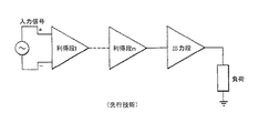
一般的に、信号源のパフォーマンスは、信号源の出力に接続された外部負荷の特性に依存する。外部負荷が可変特性を示すことが知られているときには、信号源の出力と外部負荷との間に緩衝器を設けることが望ましいことが多い。かかる緩衝器は、信号源を外部負荷から分離して、一定の中間負荷を提供し、それによって一定した信号源のパフォーマンスを確実にする。緩衝器はまた、信号源の出力に関連した優れた駆動能力を提供してもよい。増幅器および動作増幅器は、負荷依存信号源の例である。増幅器または動作増幅器は、受信信号を増幅して、増幅信号を外部負荷に与えることに使用される。増幅器または動作増幅器は通常、連続して接続された2つ以上の別個のブロックまたは段を含む。図1に示した動作増幅器の一実施例は、n個の利得ブロックと1つの出力段とを有しており、ここでnは1以上の整数である。
【0003】
当該技術分野において知られた多数の出力段の平面形状(topology)とクラスがある。多数のより一般的な出力段の平面形状を本明細書では説明する。一般的に、ダイ(die)のサイズが小さいほど生産歩留まりがよく、結果的に物理的により小さい最終製品になるので、回路設計者は、シリコン・ダイのサイズを最小化することを追求する。そのため、シリコン内で出力段を実装するのに必要な総面積は、特定の平面形状を選択するときには重要な検討事項となる。したがって、各平面形状を計測するために、特定の出力段の平面形状の相対的サイズを比較することが適正な基準である。したがって、以下の例において相対的サイズを論ずる際には、出力段において使用されるトランジスタの最小トランジスタ幾何形状(そのエミッタの面積によって通常は定められる)を、1xの単位面積を有するものとして定義する。また、出力段の最大必要出力電流は16mAと仮定する。
【0004】
1つの出力段の平面形状は、相補型エミッタ・ホロアを含み、これはOUTPUTノードに接続された負荷を駆動するために、NPNトランジスタおよびPNPトランジスタを使用しており、図2に示してある。この例のために、出力トランジスタQ1およびQ2は、それぞれが8xの面積(最小の幾何形状トランジスタの面積の8倍)を有しており、入力トランジスタQ3および電流源I1のそれぞれの最小サイズは1xであり、最大必要出力電流は16mAであると仮定する。トランジスタQ1の最大基礎電流は、電流源I1から要求される電流の量を決定する。この例において、
【数1】

【0005】
図4で分かるように、電圧源V1の一実施例は2つのトランジスタQ4およびQ5を含み、これらのそれぞれがダイオードとして接続されていて、図3の電圧源V1の必要な電圧を提供するために、トランジスタQ1およびQ2と同じエミッタ面積を有する。しかし、図3に示した実施例は、34xの総面積に、4個の大型のトランジスタ(Q1=Q2=Q4=Q5=8x)と、入力トランジスタ(Q3=1x)と、電流源(I1=1x)とを含む。したがって、この配置は、IC形式で実装するためには比較的大きなシリコン面積を必要とする。
【0006】
図4に示した出力段の別の実施例においては、電圧源V1はVBE乗算器の形式であり、後者は図3の実施例において示したトランジスタQ4およびQ5の面積よりも小さい面積を占める。VBE乗算器の2つの一般的な実施例を図4Aおよび4Bに示した。図4Aおよび4Bについて、トランジスタと電流源によって占められたシリコン面積は、それぞれ19xと20xであり、これは図3の実施例と比較して大きな削減である。しかし、図4Aおよび4Bに示したV1の実施例は、数十kΩの範囲にある抵抗R1およびR2を含み、これらの実装は6xから12xのシリコン面積を必要とするであろう。
【0007】
図2から図4に示した出力段の実施例の全てに共通な欠点は、入力信号なしの動作増幅器の通常のアイドル状態である段の零電位出力が、出力電圧に相対的な約−1.3Vの入力に対応することである。これは、トランジスタQ2およびQ3に適切にバイアスをかけるために必要である。そのため、出力での負の電圧偏差は−(|V−|−1.3V)に制限され、ここでV−は負のレールに印加される電圧である。
【0008】
図5は、出力段加回路の更に別の一般的な実施例を示しており、これは図2から4に示した実施例の出力電圧の振れの制限を克服している。しかし、図5の実施例は、全てのトランジスタが同じサイズでなければならないので、シリコン面積がより大きい(34x)ことを犠牲にして出力電圧の振れの制限を克服している。また、図5の実施例は、トランジスタQ4のエミッタにおいて、付加的な電流源I2、整合電流源I1を必要とする。
【0009】
図5の回路の34xのシリコン面積は、ダーリントン・トランジスタ対(Darlington transistor pairs)を使用することにより28xに縮小することができる。図6は、トランジスタQ1〜Q4のダーリントン対が図5のトランジスタQ1と入れ替わっており、トランジスタQ2〜Q3のダーリントン対が図5のトランジスタQ2と入れ替わっている平面形状を示している。更に、電流源I3およびI4は、ホスト動作増幅器内に既に存在していてもよく、出力段は26xのシリコン面積に更に縮小することができるであろう。
【0010】
図7に示した図6の回路の変形は、当該技術分野において知られているように、トランジスタQ7およびQ8のコレクタにおいて2つの抵抗器を付加して、2つの「ピーキング」電流源(peaking current sources)を形成している。図7の実施例の出力段の静止電流、すなわち、トランジスタQ1およびQ2のコレクタ電流は、電流源I1、I2、I3およびI4の整合および/または精度への依存が少ない。抵抗R1およびR2の値は通常小さく、結果的に、必要なシリコン面積も小さい。両方のピーキング電流源は連続しているが、R1およびR2は比較的良好に整合しなければならない。
【0011】
図6および7に示した実施例内におけるダーリントン・トランジスタの構成は、2段階の緩衝しか提供しない図5のものに比べて、第3段階の緩衝を付加しているという利点を有する。この第3段階の緩衝が、増幅器と外部負荷との間に大きな分離を付加する。しかし、図6および7の実施例は、緩衝器の出力で利用可能な最大電圧の振れを犠牲にして、付加的な分離を得ている。図5に示した回路の出力は+/−(|Vsupply|−0.85V)の電圧の振れを示すが、図6の回路の出力電圧は+/−(|Vsupply|−1.5V)だけ振れることしかできず、ここで、|Vsupply|=|V+|=|V−|である。図7の回路の出力は、抵抗R1およびR2の全体にわたる余分な電圧降下のために、更に小さく振れることしかできない。
【0012】
【発明の概要】
本発明は、外部負荷からの信号源を緩衝して分離する装置に関する。この装置は、図5に示した先行技術の装置と類似の方法で実行する出力段の形式であるが、より小さい面積を使用する。
【0013】
本発明の一実施例によれば、外部負荷からの信号源を緩衝し分離するために緩衝段が設けられている。この段は、信号源から入力信号を受け取る信号入力端子と、入力信号に対応する出力信号を外部負荷に提供する信号出力端子とを有し、
所定のバイアス電流で動作するようにそれぞれ配置された、少なくとも2つの駆動トランジスタを含む入力部と、
所定の静止電流で動作するようにそれぞれ配置された、少なくとも2つの出力トランジスタを含む出力部と、
入力部および出力部に接続されており、駆動トランジスタを通って流れるバイアス電流の大きさからはほぼ独立して、出力トランジスタを通って流れる静止電流を設定するように構成され配置された電圧源とを含む。
【0014】
一実施例においては、電圧源によって提供される電圧を調節することが、2つの駆動トランジスタを通るバイアス電流を、電圧源と一方の駆動トランジスタとを含む1つの経路と、電圧源と他方の駆動トランジスタとを含む第2の経路との間で、異なった比率で分割させる。
【0015】
一実施例においては、出力トランジスタを通る静止電流は、駆動トランジスタ(driver transistor)のそれぞれのエミッタ面積が出力トランジスタのそれぞれのエミッタ面積よりも小さい限り、駆動トランジスタのそれぞれのエミッタ面積のサイズからはほぼ独立している。
【0016】
一実施例においては、動作において、出力トランジスタのベース・エミッタ電圧の合計は、駆動トランジスタのベース・エミッタ電圧の合計に等しい。また、一実施例においては、駆動トランジスタのそれぞれのバイアス電流とコレクタ電流との間の異なった電流が、電圧源を通って流れる。
【0017】
一実施例においては、駆動トランジスタのベースは共に接続されており、緩衝段の入力を形成する。
【0018】
一実施例においては、出力トランジスタのエミッタは共に接続されており、緩衝段の出力を形成する。
【0019】
一実施例においては、緩衝段は、駆動トランジスタのそれぞれを通るバイアス電流を提供する電流源をさらに含む。
【0020】
一実施例においては、バイアス電流の少なくともいくつかが駆動トランジスタを通って流れるように、駆動トランジスタのそれぞれのエミッタは電流源に接続されている。
【0021】
一実施例においては、電圧源が駆動トランジスタのエミッタ間、ならびに出力トランジスタのベース間に接続されている。
【0022】
一実施例においては、出力トランジスタは逆の導電性タイプである。
【0023】
一実施例においては、電圧源は逆の導電性タイプの2つの電圧源トランジスタと、一方の電圧源トランジスタのコレクタと他方の電圧源トランジスタのベースとの間、ならびに他方の電圧源トランジスタのコレクタと一方の電圧源トランジスタのベースとの間に接続された抵抗器とを含む。
【0024】
一実施例においては、駆動トランジスタを通るバイアス電流は等しい。
【0025】
本発明の別の実施例によれば、出力段の全ての電流はバイアス電流源から大きく独立しており、1つのソース、すなわち電圧源から制御されている。
【0026】
好ましい一実施例においては、電圧源は単一の抵抗素子によって制御され、最終的には、出力段における全ての電流が同じ抵抗素子によって制御される。
【0027】
好ましい一実施例においては、全ての電流を提供する電圧源は、1つの駆動トランジスタの出力と1つの出力トランジスタの入力との間に接続された一方の端子、および第2の駆動トランジスタの出力と第2の出力トランジスタの入力との間に接続された他方の端子とを有する2つの端末デバイスである。
【0028】
別の実施例によれば、装置は、信号源から入力信号を受け取る信号入力端子と、入力信号に対応しており、外部負荷に出力信号を提供する信号出力端子とを含む。装置は、2つの電流源と、2つの駆動トランジスタと、2つの出力トランジスタと、制御電圧源とを含む。第1の電流源は、第1の駆動トランジスタへのエミッタ電流と、第1の出力トランジスタへのバイアス電流とを同時に提供する。第2の電流源は、第2の駆動トランジスタからのエミッタ電流と第2の出力トランジスタからのバイアス電流とを同時に受け取る。入力信号は、第1の駆動トランジスタと第2の駆動トランジスタの両方にバイアスを提供する。出力端子は、第1の出力トランジスタのエミッタと第2の出力トランジスタのエミッタの両方に電気的に接続されている。制御電圧源は、第1の駆動トランジスタのエミッタと第2の駆動トランジスタのエミッタとの間に電気的に接続されている。制御電圧源を通る電流は制御電圧の所定の関数として変化し、そのため、出力トランジスタの零入力コレクタ電流は、入力電流源および/または駆動トランジスタによって示されるあらゆるパラメータの変化にもかかわらず、ほぼ一定に保たれる。
【0029】
本発明の好ましい一実施例によれば、第1の駆動トランジスタはPNPタイプのトランジスタを含み、第2の駆動トランジスタはNPNタイプのトランジスタを含み、第1の出力トランジスタはNPNタイプのトランジスタを含み、第2の出力トランジスタはPNPタイプのトランジスタを含む。
【0030】
本発明の別の実施例においては、供給電力源は、第1の出力トランジスタのコレクタと第2の出力トランジスタのコレクタとの間に電気的に接続されている。
【0031】
別の実施例においては、所定の関数はほぼ指数的な関係を含む。
【0032】
更に別の実施例においては、制御電圧源は、抵抗器と、PNPタイプのトランジスタと、NPNタイプのトランジスタとを含む。この実施例においては、抵抗器はPNPタイプのトランジスタのコレクタとNPNタイプのトランジスタのコレクタとの間に電気的に接続されている。PNPタイプのトランジスタのベースは、NPNタイプのトランジスタのコレクタに電気的に接続されており、NPNタイプのトランジスタのベースは、PNPタイプのトランジスタのコレクタに電気的に接続されており、PNPタイプのトランジスタのエミッタは、第1の駆動トランジスタのエミッタに電気的に接続されており、NPNタイプのトランジスタのエミッタは、第2の駆動トランジスタのエミッタに電気的に接続されている。
【0033】
本発明の上記の目的および他の目的、その様々な特徴、ならびに本発明自体は、以下の詳細な説明を付属の図面と共に読めば更に完全に理解されるであろう。
【0034】
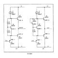
【発明の詳細な記述】
本発明は、信号源と外部負荷との間で分離を提供する改良型出力段に関する。図8に模式的に示した出力段100の好ましい一実施例は、入力部102と、出力部104と、制御電圧源106とを含む。入力部102は信号源(図示せず)から入力信号を受け取り、この入力信号の関数として出力部104の動作を制御する。出力部104は外部負荷(図示せず)に高電流駆動能力を提供し、以下で明らかになるように、制御電圧源106は入力部102および出力部104に共通の構成要素である。本発明の一実施例によれば、制御電圧源106は、入力部102と出力部104の両方においてベース・エミッタ電圧の合計を固定し、入力部102における駆動トランジスタQ3およびQ4のバイアス電流とコレクタ電流との間の相違によって定められる電流の共通の経路を提供する。
【0035】
入力部102は、PNPバイポーラ・トランジスタQ3およびNPNバイポーラ・トランジスタQ4と、第1の電流源I1と、第2の電流源I2とを含む。トランジスタQ3およびQ4のベースは、電気的に共に接続されており、入力信号を受け取るために入力ポート108に接続されている。トランジスタQ3のエミッタは第1の電流源I1の出力に電気的に接続されており、トランジスタQ3のコレクタは負の電圧レール、すなわち第1の電圧供給源V−に電気的に接続されており、第1の電流源の入力は正の電圧レール、すなわち第2の電圧供給源V+に電気的に接続されている。トランジスタQ4のコレクタは、第2の電圧供給源V+に電気的に接続されており、トランジスタQ4のエミッタは第2の電流源I2の入力に電気的に接続されており、第2の電流源I2の出力は第1の電圧供給源V−に電気的に接続されている。
【0036】
出力段100の出力部104は、NPNバイポーラ・トランジスタQ1とPNPバイポーラ・トランジスタQ2とを含む。トランジスタQ1およびQ2のエミッタは電気的に共に接続されており、出力信号を外部負荷に提供するために、出力ポート110に電気的に接続されている。トランジスタQ1のコレクタは、第2の電圧供給源V+に電気的に接続されており、トランジスタQ2のコレクタは、第1の電圧供給原V−に電気的に接続されている。トランジスタQ1のベースは、第1の電流源I1の出力とトランジスタQ3のエミッタとに電気的に接続されている。トランジスタQ2のベースは、第2の電流源12の入力とトランジスタQ4のエミッタとに電気的に接続されている。
【0037】
制御電圧源106は正の端子と負の端子とを含む。制御電圧源106の正の端子はトランジスタQ1のベースと、トランジスタQ3のエミッタと、第1の電流源I1の出力とに電気的に接続されている。制御電圧源106の負の端子は、トランジスタQ2のベースと、トランジスタQ4のエミッタと、第2の電流源I2の入力とに電気的に接続されている。
【0038】
本発明の一実施例によれば、制御電圧源106にかかる電圧V1は、所望の静止電流が出力トランジスタQ1およびQ2を通って流れるように設定される。電圧V1を調節することが、バイアス電流I1およびI2を、それぞれ、トランジスタQ3と制御電圧源106とを含む経路と、トランジスタQ4と制御電圧源106とを含む経路との間において異なった比率で分割させる。出力段100における全ての電流は、大幅に電流源I1およびI2からは独立しており、制御電圧源106にかかる電圧V1によって制御することができる。また、トランジスタQ3および制御電圧源106を含む経路と、トランジスタQ4および制御電圧源106を含む経路との間における電流の分割は、トランジスタQ3およびQ4のそれぞれのエミッタ面積を変えることにより制御できる。トランジスタQ3およびQ4のそれぞれのサイズを変えること、および/または電流源I1および/またはI2を変えることは、トランジスタQ1およびQ2を通る静止電流に影響を与えない。これは、本発明と図5に示した先行技術の出力段との間の根本的な相違である。したがって、図8の実施例において、駆動トランジスタQ3およびQ4のそれぞれのエミッタ面積が出力トランジスタQ1およびQ2のそれぞれのエミッタ面積よりも小さい限り、駆動トランジスタQ3およびQ4のそれぞれのエミッタ面積は任意であって、出力トランジスタQ1およびQ2のそれぞれのエミッタ面積からは独立しており、大きな設計の自由度を提供する。駆動トランジスタQ3およびQ4のエミッタ面積が出力トランジスタQ1およびQ2のエミッタ面積よりも小さい場合には、Q3およびQ4のコレクタ電流は図5に示した回路における対応する電流よりも少ない。余分な電流が制御電圧ソース106を通って流れる。エミッタ面積はシリコン面積を直接的に意味するので、本発明は、図5に示した先行技術の回路を実装するために使用するシリコン面積よりも比較的小さいシリコン面積を使用する。
【0039】
出力段100の詳細な動作を説明するために、以下の表記を使用する。
Ic1、Ic2、Ic3、Ic4=それぞれ、トランジスタQ1、Q2、Q3およびQ4のコレクタ電流。
IV1=電圧源V1を通る電流。
ISN=NPNトランジスタ飽和電流。
ISP=PNPトランジスタ飽和電流。
VT=熱電圧、25.9mV。
β=トランジスタ電流利得。
x=駆動トランジスタQ3およびQ4のそれぞれのエミッタ面積。
z=出力トランジスタQ1およびQ2のそれぞれのエミッタ面積。
【0040】
一般的に、全てのトランジスタQ1、Q2、Q3およびQ4のコレクタ電流は次のように表すことができる。
【数2】
【数6】
【数7】
【数8】
【数9】
【数10】
【0041】
駆動トランジスタQ3およびQ4のコレクタ電流は、バイアス制御電圧源106の関数として計算できる。トランジスタQ3およびQ4のベース・エミッタ電圧の合計は、数式(11)に示したようにV1に等しい。
【数11】
【数12】
【数13】
【数14】
【数16】
【数17】
【0042】
静止電流とドライバ・コレクタ電流との間の関係と同じ関係が、図5に示した回路にも存在する。図5の場合には、駆動トランジスタのコレクタ電流は、バイアス電流源I1およびI2の電流に等しい。バイアス電流源I1とI2とが等しければ、Ic3=Ic4=IBである。しかし、図5の回路における駆動トランジスタのエミッタ面積のサイズの変化「x」は、静止電流Iqの変化につながるであろう。これは、バイアス電流源が駆動トランジスタのみに接続されているために発生する。本発明の図8の実施例の場合には、駆動トランジスタのエミッタ面積のサイズに対する同じ変化は、静止電流Iqを変えないであろう。逆に、駆動トランジスタIc3およびIc4のコレクタ電流は、数式(17)に従って変化する。駆動トランジスタのバイアス電流とコレクタ電流との間の「差分電流」は、電圧源106を通って流れる。制御電圧源106を通る電流は、数式(16)を数式(14)に代入することにより、次のように計算できる。
【数18】
VR=抵抗Rにかかる電圧。
IR=抵抗電流。
e=自然対数ベース、e=2.718。
ノードAとBとの間の電圧は、次のように計算できる。
【数19】
【0043】
より正確な形式では、コレクタ電流および抵抗器電流は次のように定義できる。
【数21】
【0044】
数式(21)、(22)および(23)を数式(20)に代入すると、ノードAとBとの間の電圧は次のようになる。
【数24】
前述のように、ベース・エミッタ電圧と抵抗器電圧とは互いに取り消し合う傾向にあり、その取り消しが完全である特定の電流が存在する。この特定の電流は、電流に関して、ノードAとBとの間の電圧の導関数をゼロと等しくすることにより計算できる。
【数25】
V(A-B)に関する数式(24)を数式(25)に代入すると、次の数式が得られる。
【数26】
【数27】
【0047】
数式(27)のI0を数式(24)に代入すると、取り消しが完全であるノードAおよびBにかかる電圧は、次のように計算できる。
【数28】
【数29】
【数30】
図10は、数式(30)で定義された電圧V(A-B)のプロットを示している。電圧源106にかかる電圧は、それを通過する電流が比較的広い範囲で掃引するときに、比較的安定したままである。
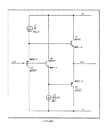
【0049】
図11および図12は、電流が50%および100%にそれぞれ変化したときに、電圧源106にかかる電圧のエラーを示している。
【0050】
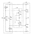
図9の電圧源の特定の実施を含む図8の回路を、図13に示した。制御電圧源106は、トランジスタQ5およびQ6ならびに抵抗器R1によって形成されている。電圧源トランジスタのエミッタ面積は、_y_として定義される。上記の表記および参照指定子を使用すると、数式(30)によって定義されたノードAおよびBにかかる電圧は、次のように表すことができる。
【数31】
【数32】
【0051】
電流IV1に関する感度が最小である、ノードAおよびBにかかる電圧は、数式(32)を数式(31)に代入することにより計算される。
【数33】
【数34】
【数35】
【数36】
【数37】
【数38】
【数39】
【0052】
数式(17)によれば、駆動トランジスタのコレクタ電流は静止電流に直線的に比例している。結果的に、駆動トランジスタのコレクタ電流は、バイアス電流に対して比較的安定しており、バイアス電流が変化した場合には、制御電圧源106(ノードAとBとの間に接続されている)を通って流れる余分な電流は、バイアス電流に直線的に比例する。この依存関係は、図16に示した。この図は、バイアス電流源出力202と、バイアス電流源出力に対する制御電圧源204および駆動トランジスタ206を通る電流とをプロットしている。バイアス電流の関数としての静止電流については分析的解は存在しないので、バイアス電流に対する静止電流の感度は計算できない。しかし、バイアス電流と電圧源を通る電流との間の直線的関係を与えられると、電圧源を通る電流に対する静止電流の感度を計算することにより、良好な推定を行うことができる。
【数40】
【数41】
【数42】
i)電圧源を通って流れる電流に対する、ノードAおよびBにかかる電圧の依存を最小にすること、およびii)バイアス電流源に対する静止電流の依存を最小にすることを介して、問題を解くことにより同じ結果に達する。
【0053】
数式(42)を数式(34)に代入すると、数式(35)に示したように、出力トランジスタに関する名目的動作点が計算される。数式(35)および(42)を数式(34)に代入すると、静止電流は以下の公式で得られる。
【数43】
【数44】
【0054】
数式(42)を数式(39)に代入すると、バイアス電流は次のようになる。
【数46】
【数47】
【数48】
【数49】
【数50】
【数51】
【数52】
【数53】
【数54】
【0055】
図5の回路に必要なトランジスタ面積は次のとおりである。
【数55】
【数56】
【数57】
【数58】
本発明は、その主旨または本質的な特徴から逸脱することなく、他の特定の形式で実施してもよい。したがって、上記の実施例は例示的であるものと考えるべきであって、限定的と捉えるべきではない。本発明の範囲は、上記の説明によってではなく特許請求の範囲によって示されており、したがって、特許請求の範囲の意味および均等の範囲内に入る全ての変更は、特許請求に範囲内に包含されることを出願人は意図している。
【図面の簡単な説明】
【図1】 典型的な先行技術の動作増幅器の略図である。
【図2】 先行技術の相補型エミッタ・フォロアの出力段アーキテクチャの略図である。
【図3】 一般的な2トランジスタ・バイアス電圧源を有する先行技術の出力段アーキテクチャの略図である。
【図4】 Aは、VBE乗算器出力段アーキテクチャの先行技術による実施の略図である。
Bは、VBE乗算器出力段アーキテクチャの別の先行技術による実施の略図である。
【図5】 先行技術の出力段アーキテクチャの更に別の一般的な実施例の略図である。
【図6】 図5に示した先行技術の出力段アーキテクチャの変形を示した略図である。
【図7】 図5に示した先行技術の出力段アーキテクチャの更に別の変形を示した略図である。
【図8】 本発明による改良型出力段アーキテクチャの略図である。
【図9】 図8の制御電圧源106の好ましい実施例の略図である。
【図10】 図9の制御電圧源にかかる電圧のグラフである。
【図11】 電流が50%変化したときの、図9の制御電圧源にかかる電圧エラーのグラフである。
【図12】 電流が100%変化した場合の、図9の制御電圧源にかかる電圧エラーのグラフである。
【図13】 図9の制御電圧源の実施例を含むように変更された、図8の出力段の略図である。
【図14】 電圧源電流の関数としての、図13の出力トランジスタを通る静止電流のグラフである。
【図15】 図13の出力トランジスタのバイアス電流に対する静止入力電流のグラフである。
【図16】 バイアス電流源出力に対する、バイアス電流源出力、制御電圧源電流、および駆動トランジスタを通る電流をプロットしたグラフである。
【図17】 制御電圧源を通る電流の変化率に対する、出力トランジスタ静止入力電流のエラー率のグラフである。[0001]
BACKGROUND OF THE INVENTION
The present invention relates to an apparatus and method for buffering and isolating a signal source from an external load, and in particular, such that the buffer and isolation characteristics are substantially independent of variations in the internal bias current source and the voltage source used internally. In particular, it relates to an apparatus and method for buffering and isolating a signal source from an external load.
[0002]
[Prior art]
In general, the performance of the signal source depends on the characteristics of the external load connected to the output of the signal source. When the external load is known to exhibit variable characteristics, it is often desirable to provide a buffer between the output of the signal source and the external load. Such a buffer isolates the signal source from the external load and provides a constant intermediate load, thereby ensuring constant signal source performance. The shock absorber may also provide superior drive capability related to the output of the signal source. Amplifiers and operational amplifiers are examples of load dependent signal sources. An amplifier or operational amplifier is used to amplify the received signal and provide the amplified signal to an external load. An amplifier or operational amplifier typically includes two or more separate blocks or stages connected in series. One embodiment of the operational amplifier shown in FIG. 1 has n gain blocks and one output stage, where n is an integer greater than or equal to one.
[0003]
There are a number of output stage topologies and classes known in the art. A number of more common output stage planar shapes are described herein. In general, circuit designers seek to minimize the size of the silicon die because the smaller the die size, the better the production yield and the resulting physically smaller end product. As such, the total area required to implement the output stage in silicon is an important consideration when selecting a particular planar shape. Therefore, in order to measure each planar shape, it is a proper standard to compare the relative sizes of the planar shapes of a specific output stage. Thus, when discussing relative sizes in the following examples, the minimum transistor geometry of a transistor used in the output stage (usually determined by its emitter area) is defined as having a unit area of 1x. . Further, it is assumed that the maximum required output current of the output stage is 16 mA.
[0004]
The planar shape of one output stage includes a complementary emitter follower, which uses an NPN transistor and a PNP transistor to drive a load connected to the OUTPUT node and is shown in FIG. For this example, output transistors Q1 and Q2 each have an area of 8x (8 times the area of the smallest geometric transistor), and the minimum size of each of input transistor Q3 and current source I1 is 1x. And the maximum required output current is assumed to be 16 mA. The maximum base current of transistor Q1 determines the amount of current required from current source I1. In this example,
[Expression 1]
[0005]
As can be seen in FIG. 4, one embodiment of voltage source V1 includes two transistors Q4 and Q5, each of which is connected as a diode to provide the required voltage of voltage source V1 of FIG. Have the same emitter area as transistors Q1 and Q2. However, the embodiment shown in FIG. 3 has a total area of 34x, four large transistors (Q1 = Q2 = Q4 = Q5 = 8x), an input transistor (Q3 = 1x), and a current source (I1 = 1x). Therefore, this arrangement requires a relatively large silicon area for mounting in IC form.
[0006]
In another embodiment of the output stage shown in FIG. 4, the voltage source V1 is VBEIn the form of a multiplier, the latter occupies an area smaller than the areas of the transistors Q4 and Q5 shown in the embodiment of FIG. VBETwo general embodiments of the multiplier are shown in FIGS. 4A and 4B. For FIGS. 4A and 4B, the silicon area occupied by the transistor and the current source is 19x and 20x, respectively, which is a significant reduction compared to the embodiment of FIG. However, the V1 embodiment shown in FIGS. 4A and 4B includes resistors R1 and R2 in the range of tens of kΩ, and these implementations would require 6x to 12x silicon area.
[0007]
A disadvantage common to all of the embodiments of the output stage shown in FIGS. 2-4 is that the zero potential output of the stage that is the normal idle state of an operational amplifier without an input signal is approximately −1 relative to the output voltage. .3V input. This is necessary to properly bias transistors Q2 and Q3. Therefore, the negative voltage deviation at the output is limited to-(| V- | -1.3V), where V- is the voltage applied to the negative rail.
[0008]
FIG. 5 shows yet another general embodiment of the output stage adder circuit, which overcomes the output voltage swing limitations of the embodiments shown in FIGS. However, the embodiment of FIG. 5 overcomes the output voltage swing limitation at the expense of a larger silicon area (34x) because all transistors must be the same size. 5 requires an additional current source I2 and a matching current source I1 at the emitter of transistor Q4.
[0009]
The 34x silicon area of the circuit of FIG. 5 can be reduced to 28x by using Darlington transistor pairs. FIG. 6 shows a planar shape in which the Darlington pair of the transistors Q1 to Q4 is replaced with the transistor Q1 in FIG. 5, and the Darlington pair of the transistors Q2 to Q3 is replaced with the transistor Q2 in FIG. Furthermore, current sources I3 and I4 may already be present in the host operational amplifier, and the output stage could be further reduced to 26x silicon area.
[0010]
A variation of the circuit of FIG. 6 shown in FIG. 7 is that two “peaking” current sources are added, adding two resistors at the collectors of transistors Q7 and Q8, as is known in the art. sources). The output stage quiescent current of the embodiment of FIG. 7, ie, the collector currents of transistors Q1 and Q2, is less dependent on the matching and / or accuracy of current sources I1, I2, I3 and I4. The values of the resistors R1 and R2 are usually small and consequently the required silicon area is also small. Both peaking current sources are continuous, but R1 and R2 must be relatively well matched.
[0011]
The Darlington transistor configuration within the embodiment shown in FIGS. 6 and 7 has the advantage of adding a third stage buffer compared to that of FIG. 5 which provides only a two stage buffer. This third stage buffer adds significant isolation between the amplifier and the external load. However, the embodiment of FIGS. 6 and 7 provides additional isolation at the expense of the maximum voltage swing available at the output of the buffer. The output of the circuit shown in FIG. 5 is +/− (| Vsupply| −0.85V), the output voltage of the circuit of FIG. 6 is +/− (| Vsupply| −1.5V), where | Vsupply| = | V + | = | V− |. The output of the circuit of FIG. 7 can only swing smaller due to the extra voltage drop across resistors R1 and R2.
[0012]
SUMMARY OF THE INVENTION
The present invention relates to an apparatus for buffering and separating a signal source from an external load. This device is in the form of an output stage that performs in a manner similar to the prior art device shown in FIG. 5, but uses a smaller area.
[0013]
According to one embodiment of the present invention, a buffer stage is provided to buffer and isolate the signal source from the external load. This stage has a signal input terminal that receives an input signal from a signal source, and a signal output terminal that provides an output signal corresponding to the input signal to an external load,
An input unit including at least two drive transistors, each arranged to operate with a predetermined bias current;
An output including at least two output transistors, each arranged to operate with a predetermined quiescent current;
A voltage source connected to the input and output and configured and arranged to set a quiescent current flowing through the output transistor, substantially independent of the magnitude of the bias current flowing through the drive transistor; including.
[0014]
In one embodiment, adjusting the voltage provided by the voltage source allows bias current through the two drive transistors, one path including the voltage source and one drive transistor, and the voltage source and the other drive. The second path including the transistor is divided at a different ratio.
[0015]
In one embodiment, the quiescent current through the output transistor is approximately from the size of the respective emitter area of the drive transistor as long as the respective emitter area of the driver transistor is smaller than the respective emitter area of the output transistor. being independent.
[0016]
In one embodiment, in operation, the sum of the base-emitter voltages of the output transistors is equal to the sum of the base-emitter voltages of the drive transistors. Also, in one embodiment, a different current between each bias current and collector current of the drive transistor flows through the voltage source.
[0017]
In one embodiment, the bases of the drive transistors are connected together to form the buffer stage input.
[0018]
In one embodiment, the emitters of the output transistors are connected together to form the output of the buffer stage.
[0019]
In one embodiment, the buffer stage further includes a current source that provides a bias current through each of the drive transistors.
[0020]
In one embodiment, each emitter of the drive transistor is connected to a current source so that at least some of the bias current flows through the drive transistor.
[0021]
In one embodiment, a voltage source is connected between the emitters of the drive transistors and between the bases of the output transistors.
[0022]
In one embodiment, the output transistor is of the opposite conductivity type.
[0023]
In one embodiment, the voltage source includes two voltage source transistors of opposite conductivity type, between the collector of one voltage source transistor and the base of the other voltage source transistor, and the collector of the other voltage source transistor. A resistor connected between the base of one of the voltage source transistors.
[0024]
In one embodiment, the bias current through the drive transistor is equal.
[0025]
According to another embodiment of the invention, all currents in the output stage are largely independent of the bias current source and are controlled from one source, the voltage source.
[0026]
In a preferred embodiment, the voltage source is controlled by a single resistive element, and ultimately all currents in the output stage are controlled by the same resistive element.
[0027]
In a preferred embodiment, the voltage source providing all the current is one terminal connected between the output of one drive transistor and the input of one output transistor, and the output of the second drive transistor. Two terminal devices having the other terminal connected between the input of the second output transistor.
[0028]
According to another embodiment, the apparatus includes a signal input terminal that receives an input signal from a signal source, and a signal output terminal that is responsive to the input signal and provides an output signal to an external load. The apparatus includes two current sources, two drive transistors, two output transistors, and a control voltage source. The first current source simultaneously provides an emitter current to the first drive transistor and a bias current to the first output transistor. The second current source simultaneously receives the emitter current from the second drive transistor and the bias current from the second output transistor. The input signal provides a bias for both the first drive transistor and the second drive transistor. The output terminal is electrically connected to both the emitter of the first output transistor and the emitter of the second output transistor. The control voltage source is electrically connected between the emitter of the first drive transistor and the emitter of the second drive transistor. The current through the control voltage source varies as a predetermined function of the control voltage, so that the quiescent collector current of the output transistor is approximately constant despite changes in any parameters exhibited by the input current source and / or drive transistor. To be kept.
[0029]
According to a preferred embodiment of the present invention, the first driving transistor includes a PNP type transistor, the second driving transistor includes an NPN type transistor, and the first output transistor includes an NPN type transistor; The second output transistor includes a PNP type transistor.
[0030]
In another embodiment of the invention, the supply power source is electrically connected between the collector of the first output transistor and the collector of the second output transistor.
[0031]
In another embodiment, the predetermined function includes a substantially exponential relationship.
[0032]
In yet another embodiment, the control voltage source includes a resistor, a PNP type transistor, and an NPN type transistor. In this embodiment, the resistor is electrically connected between the collector of the PNP type transistor and the collector of the NPN type transistor. The base of the PNP type transistor is electrically connected to the collector of the NPN type transistor, and the base of the NPN type transistor is electrically connected to the collector of the PNP type transistor. The emitter of the NPN transistor is electrically connected to the emitter of the first driving transistor, and the emitter of the NPN type transistor is electrically connected to the emitter of the second driving transistor.
[0033]
The above and other objects of the invention, its various features, and the invention itself will be more fully understood when the following detailed description is read in conjunction with the accompanying drawings.
[0034]
Detailed Description of the Invention
The present invention relates to an improved output stage that provides isolation between a signal source and an external load. A preferred embodiment of the
[0035]
[0036]
The
[0037]
[0038]
According to one embodiment of the present invention, the voltage V1 across the
[0039]
To describe the detailed operation of the
Ic1, Ic2, Ic3, Ic4= Collector currents of transistors Q1, Q2, Q3 and Q4, respectively.
IV1= Current through voltage source V1.
ISN= NPN transistor saturation current.
ISP= PNP transistor saturation current.
VT= Thermal voltage, 25.9 mV.
β = transistor current gain.
x = emitter area of each of the drive transistors Q3 and Q4.
z = emitter area of each of output transistors Q1 and Q2.
[0040]
In general, the collector currents of all transistors Q1, Q2, Q3 and Q4 can be expressed as:
[Expression 2]
[Formula 6]
[Expression 7]
[Equation 8]
[Equation 9]
[Expression 10]
[0041]
The collector currents of the drive transistors Q3 and Q4 can be calculated as a function of the bias
## EQU11 ##
[Expression 12]
[Formula 13]
[Expression 14]
[Expression 16]
[Expression 17]
[0042]
The same relationship between quiescent current and driver-collector current also exists in the circuit shown in FIG. In the case of FIG. 5, the collector current of the driving transistor is equal to the currents of the bias current sources I1 and I2. If the bias current sources I1 and I2 are equal, Ic3= Ic4= IBIt is. However, the change “x” in the size of the emitter area of the driving transistor in the circuit of FIG.qWill lead to changes. This occurs because the bias current source is connected only to the drive transistor. For the embodiment of FIG. 8 of the present invention, the same change to the size of the emitter area of the drive transistor is the quiescent current IqWill not change. Conversely, the drive transistor Ic3And Ic4The collector current of varies according to equation (17). A “difference current” between the bias current and collector current of the drive transistor flows through the
[Expression 18]
VR= Voltage applied to resistor R.
IR= Resistance current.
e = natural log base, e = 2.718.
The voltage between nodes A and B can be calculated as follows:
[Equation 19]
[0043]
In a more precise form, the collector current and resistor current can be defined as follows:
[Expression 21]
[0044]
Substituting Equations (21), (22), and (23) into Equation (20), the voltage between nodes A and B is as follows:
[Expression 24]
As mentioned above, there is a specific current where the base-emitter voltage and the resistor voltage tend to cancel each other and the cancellation is complete. This particular current can be calculated by making the derivative of the voltage between nodes A and B equal to zero with respect to the current.
[Expression 25]
V(AB)Substituting the mathematical formula (24) for the mathematical formula (25), the following mathematical formula is obtained.
[Equation 26]
[Expression 27]
[0047]
I in Equation (27)0Is substituted into equation (24), the voltage applied to nodes A and B for which cancellation is complete can be calculated as follows.
[Expression 28]
[Expression 29]
[30]
FIG. 10 shows the voltage V defined by Equation (30).(AB)The plot of is shown. The voltage across the
[0049]
11 and 12 show the voltage error across the
[0050]
The circuit of FIG. 8 including a specific implementation of the voltage source of FIG. 9 is shown in FIG.
[31]
[Expression 32]
[0051]
Current IV1The voltage across nodes A and B with the least sensitivity is calculated by substituting equation (32) into equation (31).
[Expression 33]
[Expression 34]
[Expression 35]
[Expression 36]
[Expression 37]
[Formula 38]
[39]
[0052]
According to Equation (17), the collector current of the driving transistor is linearly proportional to the quiescent current. As a result, the collector current of the driving transistor is relatively stable with respect to the bias current, and when the bias current changes, the control voltage source 106 (connected between the nodes A and B). The excess current flowing through is linearly proportional to the bias current. This dependency is shown in FIG. The figure plots the bias
[Formula 40]
[Expression 41]
[Expression 42]
i) Solving the problem through minimizing the voltage dependence on nodes A and B to the current flowing through the voltage source, and ii) minimizing the quiescent current dependence on the bias current source. To achieve the same result.
[0053]
Substituting equation (42) into equation (34), the nominal target operating point for the output transistor is calculated as shown in equation (35). Substituting Equations (35) and (42) into Equation (34), the quiescent current can be obtained by the following formula.
[Expression 43]
(44)
[0054]
Substituting Equation (42) into Equation (39) yields the bias current as follows:
[Equation 46]
[Equation 47]
[Formula 48]
[Formula 49]
[Equation 50]
[Equation 51]
[Formula 52]
[Equation 53]
[Formula 54]
[0055]
The transistor area required for the circuit of FIG. 5 is as follows.
[Expression 55]
[56]
[Equation 57]
[Formula 58]
The present invention may be embodied in other specific forms without departing from its spirit or essential characteristics. Accordingly, the above embodiments should be considered illustrative and not limiting. The scope of the present invention is shown not by the above description but by the claims, and all changes that come within the meaning and range of equivalency of the claims are to be embraced within the scope of the claims. The applicant intends to do so.
[Brief description of the drawings]
FIG. 1 is a schematic diagram of a typical prior art operational amplifier.
FIG. 2 is a schematic diagram of a prior art complementary emitter follower output stage architecture.
FIG. 3 is a schematic diagram of a prior art output stage architecture with a typical two-transistor bias voltage source.
FIG. 4A is
B is VBEFigure 3 is a schematic representation of another prior art implementation of a multiplier output stage architecture.
FIG. 5 is a schematic diagram of yet another general embodiment of a prior art output stage architecture.
6 is a schematic diagram illustrating a variation of the prior art output stage architecture shown in FIG.
7 is a schematic diagram illustrating yet another variation of the prior art output stage architecture shown in FIG.
FIG. 8 is a schematic diagram of an improved output stage architecture according to the present invention.
FIG. 9 is a schematic diagram of a preferred embodiment of the
10 is a graph of a voltage applied to the control voltage source of FIG.
FIG. 11 is a graph of a voltage error applied to the control voltage source of FIG. 9 when the current changes by 50%.
12 is a graph of a voltage error applied to the control voltage source of FIG. 9 when the current changes by 100%.
13 is a schematic diagram of the output stage of FIG. 8, modified to include the embodiment of the control voltage source of FIG.
14 is a graph of quiescent current through the output transistor of FIG. 13 as a function of voltage source current.
15 is a graph of quiescent input current versus bias current for the output transistor of FIG.
FIG. 16 is a graph plotting bias current source output, control voltage source current, and current through a drive transistor against bias current source output.
FIG. 17 is a graph of the error rate of the output transistor quiescent input current versus the rate of change of current through the control voltage source.
Claims (20)
第1のエミッタ電流を第1の駆動トランジスタに提供し、第1のバイアス電流を第1の出力トランジスタに提供する第1のバイアス電流源と、
第2のエミッタ電流を第2の駆動トランジスタから受け取り、第2のバイアス電流を第2の出力トランジスタから受け取る第2のバイアス電流源とからなり、該入力信号は該第1の駆動トランジスタと該第2の駆動トランジスタにバイアスをかけ、該出力端子は該第1の出力トランジスタのエミッタと該第2の出力トランジスタのエミッタとに電気的に接続されており、該装置はさらに、
制御電圧源を通じて流れる制御電流と制御電圧源にわたる制御電圧により特徴付けられる制御電圧源であって、該制御電圧は、制御電流の様々な値について一定に保たれ、該制御電圧源は、該第1の駆動トランジスタのエミッタと該第2の駆動トランジスタのエミッタとの間に電気的に接続され、該第1のバイアス電流と該第2のバイアス電流は、該制御電圧の所定の関数として変化し、
該第1及び第2の駆動トランジスタの各々のエミッタ面積は、該第1及び第2の出力トランジスタの各々のエミッタ面積より小さいことを特徴とする装置。An apparatus for buffering and separating a signal source from an external load, the apparatus providing a signal input terminal for receiving an input signal from the signal source and an output signal corresponding to the input signal to the external load. A signal output terminal, the device further comprising:
A first bias current source that provides a first emitter current to the first drive transistor and a first bias current to the first output transistor;
A second bias current source receiving a second emitter current from the second drive transistor and receiving a second bias current from the second output transistor, the input signal being the first drive transistor and the second drive transistor; The second drive transistor is biased, and the output terminal is electrically connected to the emitter of the first output transistor and the emitter of the second output transistor, the device further comprising:
A control voltage source characterized by a control current flowing through the control voltage source and a control voltage across the control voltage source, the control voltage being kept constant for various values of the control current, the control voltage source being Electrically connected between the emitter of one drive transistor and the emitter of the second drive transistor, and the first bias current and the second bias current vary as a predetermined function of the control voltage. ,
An apparatus wherein the emitter area of each of the first and second drive transistors is less than the emitter area of each of the first and second output transistors.
第1の静止コレクタ電流を有する第1のNPNタイプのトランジスタと、第2の静止コレクタ電流を有する第1のPNPタイプのトランジスタとを含む出力段からなり、該第1のNPNタイプのトランジスタのエミッタは該第1のPNPタイプのトランジスタのエミッタに電気的に接続されており、該第1のNPNタイプのトランジスタのコレクタは第1の電圧供給源に接続されており、該第1のPNPタイプのトランジスタのコレクタは第2の電圧供給源に接続されており、該装置はさらに、
入力段からなり、該入力段は、
I.第2のPNPタイプのトランジスタと第1の電流源とを含み、第2のPNPタイプのトランジスタのエミッタは第1の電流源出力端子と第1のNPNタイプのトランジスタのベースとに電気的に接続されており、第2のPNPタイプのトランジスタのコレクタは該第2の電圧供給源に電気的に接続されており、第2のPNPタイプのトランジスタのベースは該信号入力端子に電気的に接続されており、第1の電流源入力端子は該第1の電圧供給源に電気的に接続されており、
II.第2のNPNタイプのトランジスタと第2の電流源とを含み、第2のNPNタイプのトランジスタのエミッタは第2の電流源入力端子と第1のPNPタイプのトランジスタのベースとに電気的に接続されており、第2のNPNタイプのトランジスタのコレクタは該第1の電圧供給源に電気的に接続されており、第2のNPNタイプのトランジスタのベースは該信号入力端子に電気的に接続されており、第2の電流源出力端子は該第2の電圧供給源に電気的に接続されているものであり、該装置はさらに、
制御電圧源を通じて流れる制御電流と制御電圧源にわたる制御電圧により特徴付けられる制御電圧源からなり、
該制御電圧は、制御電流の様々な値について一定に保たれ、該制御電圧源は正の端子と負の端子とを有しており、該正の端子は該第1のNPNタイプのトランジスタのベースに電気的に接続されており、該負の端子は該第1のPNPタイプのトランジスタのベースに電気的に接続されており、該第1の静止コレクタ電流と該第2の静止コレクタ電流とは、該制御電圧の所定の関数として変化し、
該第2のNPNおよびPNPトランジスタの各々のエミッタ面積は、該第1のNPNおよびPNPトランジスタの各々のエミッタ面積より小さいことを特徴とする装置。An apparatus for buffering and separating a signal source from an external load, the apparatus having a signal input terminal for receiving an input signal from the signal source and a signal output terminal for providing an output signal to the external load. The device further comprises:
An output stage comprising a first NPN type transistor having a first quiescent collector current and a first PNP type transistor having a second quiescent collector current, the emitter of the first NPN type transistor Is electrically connected to the emitter of the first PNP type transistor, the collector of the first NPN type transistor is connected to a first voltage supply, and the first PNP type transistor is connected to the emitter of the first PNP type transistor. The collector of the transistor is connected to a second voltage supply, the device further comprising:
It consists of an input stage, which is
I. A second PNP type transistor and a first current source, wherein the emitter of the second PNP type transistor is electrically connected to the first current source output terminal and the base of the first NPN type transistor; The collector of the second PNP type transistor is electrically connected to the second voltage supply source, and the base of the second PNP type transistor is electrically connected to the signal input terminal. The first current source input terminal is electrically connected to the first voltage supply source;
II. A second NPN type transistor and a second current source, the emitter of the second NPN type transistor being electrically connected to the second current source input terminal and the base of the first PNP type transistor; The collector of the second NPN type transistor is electrically connected to the first voltage supply source, and the base of the second NPN type transistor is electrically connected to the signal input terminal. And the second current source output terminal is electrically connected to the second voltage supply source, and the apparatus further includes:
A control voltage source characterized by a control current flowing through the control voltage source and a control voltage across the control voltage source,
The control voltage is kept constant for various values of control current, and the control voltage source has a positive terminal and a negative terminal, the positive terminal of the first NPN type transistor. Electrically connected to a base, and the negative terminal is electrically connected to the base of the first PNP-type transistor, and the first quiescent collector current and the second quiescent collector current Varies as a predetermined function of the control voltage,
An apparatus wherein the emitter area of each of the second NPN and PNP transistors is less than the emitter area of each of the first NPN and PNP transistors .
所定のバイアス電流で動作するようにそれぞれ配置された少なくとも2つの駆動トランジスタを含む入力部と、
所定の静止電流で動作するようにそれぞれ配置された少なくとも2つの出力トランジスタを含む出力部と、
電圧源を通じて流れる制御電流と電圧源にわたる制御電圧により特徴付けられる制御電圧源からなり、
該制御電圧は、制御電流の様々な値について一定に保たれ、該電圧源は、該入力部と該出力部とに接続されており、該駆動トランジスタを通って流れるバイアス電流の大きさからはほぼ独立して、該出力トランジスタを通って流れる静止電流を設定するように構成され配置され、
該駆動トランジスタの各々のエミッタ面積は、該出力トランジスタの各々のエミッタ面積より小さいことを特徴とする緩衝段。A buffer stage for buffering and isolating a signal source from an external load, the buffer stage providing a signal input terminal for receiving an input signal from the signal source and an output signal corresponding to the input signal to the external load A signal output terminal, and the buffer stage includes:
An input including at least two drive transistors each arranged to operate with a predetermined bias current;
An output including at least two output transistors, each arranged to operate with a predetermined quiescent current;
A control voltage source characterized by a control current flowing through the voltage source and a control voltage across the voltage source,
The control voltage is kept constant for various values of control current, and the voltage source is connected to the input and output , and from the magnitude of the bias current flowing through the drive transistor. Configured and arranged to set a quiescent current flowing through the output transistor substantially independently ,
A buffer stage, wherein the emitter area of each of the drive transistors is smaller than the emitter area of each of the output transistors.
Applications Claiming Priority (3)
| Application Number | Priority Date | Filing Date | Title |
|---|---|---|---|
| US09/293,033 | 1999-04-16 | ||
| US09/293,033 US6160451A (en) | 1999-04-16 | 1999-04-16 | Operational amplifier output stage |
| PCT/US2000/009992 WO2000064043A1 (en) | 1999-04-16 | 2000-04-14 | Improved operational amplifier output stage |
Publications (3)
| Publication Number | Publication Date |
|---|---|
| JP2002542700A JP2002542700A (en) | 2002-12-10 |
| JP2002542700A5 JP2002542700A5 (en) | 2007-06-14 |
| JP4718016B2 true JP4718016B2 (en) | 2011-07-06 |
Family
ID=23127346
Family Applications (1)
| Application Number | Title | Priority Date | Filing Date |
|---|---|---|---|
| JP2000613068A Expired - Fee Related JP4718016B2 (en) | 1999-04-16 | 2000-04-14 | Improved operational amplifier output stage |
Country Status (9)
| Country | Link |
|---|---|
| US (1) | US6160451A (en) |
| EP (1) | EP1088391B1 (en) |
| JP (1) | JP4718016B2 (en) |
| CN (1) | CN1229912C (en) |
| DE (1) | DE60042386D1 (en) |
| EA (1) | EA003440B1 (en) |
| ES (1) | ES2329869T3 (en) |
| HK (1) | HK1038992A1 (en) |
| WO (1) | WO2000064043A1 (en) |
Families Citing this family (7)
| Publication number | Priority date | Publication date | Assignee | Title |
|---|---|---|---|---|
| US6586998B2 (en) * | 2001-03-02 | 2003-07-01 | Micrel, Incorporated | Output stage and method of enhancing output gain |
| GB0203605D0 (en) * | 2002-02-15 | 2002-04-03 | Wood John | Hierarchical clocking system |
| FR2851859B1 (en) * | 2003-02-27 | 2006-03-03 | St Microelectronics Sa | INTERFACE CIRCUIT |
| US7224227B1 (en) * | 2005-01-12 | 2007-05-29 | National Semiconductor Corporation | Apparatus and method for correction of error caused by reverse saturation current mismatch |
| JP5042500B2 (en) * | 2006-01-18 | 2012-10-03 | 新日本無線株式会社 | Operational amplifier |
| DE102009055891A1 (en) * | 2009-11-26 | 2011-06-09 | Siemens Aktiengesellschaft | Broadband, high-linearity LED amplifier with high output in a compact design |
| US20120007660A1 (en) * | 2010-07-08 | 2012-01-12 | Derek Hummerston | Bias Current Generator |
Citations (8)
| Publication number | Priority date | Publication date | Assignee | Title |
|---|---|---|---|---|
| JPS6182510A (en) * | 1984-09-29 | 1986-04-26 | Toshiba Corp | Voltage source circuit |
| JPS62100007A (en) * | 1985-10-25 | 1987-05-09 | Masaki Fujimaki | Bias circuit in fet complementary compensation circuit |
| JPS63172509A (en) * | 1987-01-09 | 1988-07-16 | Matsushita Electric Ind Co Ltd | Buffer circuit |
| JPH02186706A (en) * | 1988-11-10 | 1990-07-23 | Burr Brown Corp | Bias voltage generating circuit and method thereof |
| JPH0319412A (en) * | 1989-05-12 | 1991-01-28 | Burr Brown Corp | Unity-gain amplifier having high slew rate and high band width |
| JPH04314206A (en) * | 1991-04-12 | 1992-11-05 | Sony Corp | Driving circuit |
| US5323122A (en) * | 1993-11-02 | 1994-06-21 | Analog Devices, Inc. | Rapid slewing unity gain buffer amplifier with boosted parasitic capacitance charging |
| JPH06204759A (en) * | 1993-01-08 | 1994-07-22 | Toyota Motor Corp | Push-pull circuit |
Family Cites Families (3)
| Publication number | Priority date | Publication date | Assignee | Title |
|---|---|---|---|---|
| US4502020A (en) * | 1983-10-26 | 1985-02-26 | Comlinear Corporation | Settling time reduction in wide-band direct-coupled transistor amplifiers |
| US5418495A (en) * | 1994-05-18 | 1995-05-23 | Elantec | Input stage improvement for current feedback amplifiers |
| US5614866A (en) * | 1994-10-25 | 1997-03-25 | Elantec, Inc. | Ultra high gain amplifier |
-
1999
- 1999-04-16 US US09/293,033 patent/US6160451A/en not_active Expired - Lifetime
-
2000
- 2000-04-14 EA EA200100046A patent/EA003440B1/en not_active IP Right Cessation
- 2000-04-14 ES ES00928172T patent/ES2329869T3/en not_active Expired - Lifetime
- 2000-04-14 DE DE60042386T patent/DE60042386D1/en not_active Expired - Lifetime
- 2000-04-14 EP EP00928172A patent/EP1088391B1/en not_active Expired - Lifetime
- 2000-04-14 WO PCT/US2000/009992 patent/WO2000064043A1/en active Application Filing
- 2000-04-14 JP JP2000613068A patent/JP4718016B2/en not_active Expired - Fee Related
- 2000-04-14 CN CN00800597.4A patent/CN1229912C/en not_active Expired - Lifetime
-
2001
- 2001-12-20 HK HK01108947A patent/HK1038992A1/en unknown
Patent Citations (8)
| Publication number | Priority date | Publication date | Assignee | Title |
|---|---|---|---|---|
| JPS6182510A (en) * | 1984-09-29 | 1986-04-26 | Toshiba Corp | Voltage source circuit |
| JPS62100007A (en) * | 1985-10-25 | 1987-05-09 | Masaki Fujimaki | Bias circuit in fet complementary compensation circuit |
| JPS63172509A (en) * | 1987-01-09 | 1988-07-16 | Matsushita Electric Ind Co Ltd | Buffer circuit |
| JPH02186706A (en) * | 1988-11-10 | 1990-07-23 | Burr Brown Corp | Bias voltage generating circuit and method thereof |
| JPH0319412A (en) * | 1989-05-12 | 1991-01-28 | Burr Brown Corp | Unity-gain amplifier having high slew rate and high band width |
| JPH04314206A (en) * | 1991-04-12 | 1992-11-05 | Sony Corp | Driving circuit |
| JPH06204759A (en) * | 1993-01-08 | 1994-07-22 | Toyota Motor Corp | Push-pull circuit |
| US5323122A (en) * | 1993-11-02 | 1994-06-21 | Analog Devices, Inc. | Rapid slewing unity gain buffer amplifier with boosted parasitic capacitance charging |
Also Published As
| Publication number | Publication date |
|---|---|
| CN1300465A (en) | 2001-06-20 |
| EP1088391A4 (en) | 2004-11-24 |
| WO2000064043A1 (en) | 2000-10-26 |
| DE60042386D1 (en) | 2009-07-30 |
| JP2002542700A (en) | 2002-12-10 |
| EA003440B1 (en) | 2003-04-24 |
| EA200100046A1 (en) | 2002-02-28 |
| EP1088391B1 (en) | 2009-06-17 |
| CN1229912C (en) | 2005-11-30 |
| US6160451A (en) | 2000-12-12 |
| EP1088391A1 (en) | 2001-04-04 |
| ES2329869T3 (en) | 2009-12-02 |
| WO2000064043A8 (en) | 2001-06-21 |
| HK1038992A1 (en) | 2002-04-04 |
Similar Documents
| Publication | Publication Date | Title |
|---|---|---|
| JPH0758525B2 (en) | Magnetic recording detection circuit | |
| JPS6142965B2 (en) | ||
| GB2122831A (en) | Voltage to current converting amplifiers | |
| JP4718016B2 (en) | Improved operational amplifier output stage | |
| US5162751A (en) | Amplifier arrangement | |
| JP2869664B2 (en) | Current amplifier | |
| JP5001822B2 (en) | Bias circuit, differential amplifier | |
| US5638026A (en) | High input impedance circuit and semiconductor integrated device provided therewith | |
| JP3098451B2 (en) | Amplifier circuit | |
| JP2002108464A (en) | Constant current circuit | |
| JP3140107B2 (en) | Differential amplifier | |
| JP2623954B2 (en) | Variable gain amplifier | |
| JPS5816206B2 (en) | constant current circuit | |
| JP2609749B2 (en) | Current supply circuit | |
| JPH0227622Y2 (en) | ||
| JP2703953B2 (en) | Current amplifier circuit | |
| JP3547895B2 (en) | Constant current generation circuit | |
| JP2722769B2 (en) | Gain control circuit | |
| JPS6223133Y2 (en) | ||
| JPH0345568B2 (en) | ||
| KR20010016446A (en) | High-accuracy Transresistance amplifier | |
| JPS6133006A (en) | Agc circuit | |
| JPH04329706A (en) | Differential amplifier circuit | |
| JPS6217956B2 (en) | ||
| JPH10161760A (en) | Constant voltage generation circuit |
Legal Events
| Date | Code | Title | Description |
|---|---|---|---|
| A521 | Request for written amendment filed |
Free format text: JAPANESE INTERMEDIATE CODE: A523 Effective date: 20040323 |
|
| A521 | Request for written amendment filed |
Free format text: JAPANESE INTERMEDIATE CODE: A523 Effective date: 20070413 |
|
| A621 | Written request for application examination |
Free format text: JAPANESE INTERMEDIATE CODE: A621 Effective date: 20070413 |
|
| A977 | Report on retrieval |
Free format text: JAPANESE INTERMEDIATE CODE: A971007 Effective date: 20090820 |
|
| A131 | Notification of reasons for refusal |
Free format text: JAPANESE INTERMEDIATE CODE: A131 Effective date: 20090824 |
|
| A601 | Written request for extension of time |
Free format text: JAPANESE INTERMEDIATE CODE: A601 Effective date: 20091124 |
|
| A602 | Written permission of extension of time |
Free format text: JAPANESE INTERMEDIATE CODE: A602 Effective date: 20091201 |
|
| A521 | Request for written amendment filed |
Free format text: JAPANESE INTERMEDIATE CODE: A523 Effective date: 20100224 |
|
| RD02 | Notification of acceptance of power of attorney |
Free format text: JAPANESE INTERMEDIATE CODE: A7422 Effective date: 20100224 |
|
| A521 | Request for written amendment filed |
Free format text: JAPANESE INTERMEDIATE CODE: A821 Effective date: 20100224 |
|
| A02 | Decision of refusal |
Free format text: JAPANESE INTERMEDIATE CODE: A02 Effective date: 20100906 |
|
| A521 | Request for written amendment filed |
Free format text: JAPANESE INTERMEDIATE CODE: A523 Effective date: 20101224 |
|
| A911 | Transfer to examiner for re-examination before appeal (zenchi) |
Free format text: JAPANESE INTERMEDIATE CODE: A911 Effective date: 20110107 |
|
| A01 | Written decision to grant a patent or to grant a registration (utility model) |
Free format text: JAPANESE INTERMEDIATE CODE: A01 Effective date: 20110307 |
|
| A61 | First payment of annual fees (during grant procedure) |
Free format text: JAPANESE INTERMEDIATE CODE: A61 Effective date: 20110331 |
|
| R150 | Certificate of patent or registration of utility model |
Free format text: JAPANESE INTERMEDIATE CODE: R150 |
|
| FPAY | Renewal fee payment (event date is renewal date of database) |
Free format text: PAYMENT UNTIL: 20140408 Year of fee payment: 3 |
|
| LAPS | Cancellation because of no payment of annual fees |