JP4666100B2 - Drive device - Google Patents

Drive device Download PDF

Info

Publication number
JP4666100B2
JP4666100B2 JP2009298540A JP2009298540A JP4666100B2 JP 4666100 B2 JP4666100 B2 JP 4666100B2 JP 2009298540 A JP2009298540 A JP 2009298540A JP 2009298540 A JP2009298540 A JP 2009298540A JP 4666100 B2 JP4666100 B2 JP 4666100B2
Authority
JP
Japan
Prior art keywords
drive
circuit
switch
piezoelectric element
driving
Prior art date
Legal status (The legal status is an assumption and is not a legal conclusion. Google has not performed a legal analysis and makes no representation as to the accuracy of the status listed.)
Expired - Lifetime
Application number
JP2009298540A
Other languages
Japanese (ja)
Other versions
JP2010104231A (en
Inventor
智行 湯淺
龍一 吉田
治行 中野
Current Assignee (The listed assignees may be inaccurate. Google has not performed a legal analysis and makes no representation or warranty as to the accuracy of the list.)
Konica Minolta Inc
Original Assignee
Konica Minolta Inc
Priority date (The priority date is an assumption and is not a legal conclusion. Google has not performed a legal analysis and makes no representation as to the accuracy of the date listed.)
Filing date
Publication date
Application filed by Konica Minolta Inc filed Critical Konica Minolta Inc
Priority to JP2009298540A priority Critical patent/JP4666100B2/en
Publication of JP2010104231A publication Critical patent/JP2010104231A/en
Application granted granted Critical
Publication of JP4666100B2 publication Critical patent/JP4666100B2/en
Anticipated expiration legal-status Critical
Expired - Lifetime legal-status Critical Current

Links

Images

Description

本発明は、駆動装置に関し、特にはXY移動ステージ、カメラの撮影レンズ、オーバヘッドプロジェクタの投影レンズ、双眼鏡のレンズ等の駆動に適した駆動装置に関する。   The present invention relates to a driving device, and more particularly to a driving device suitable for driving an XY moving stage, a camera photographing lens, a projection lens of an overhead projector, a binocular lens, and the like.

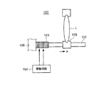
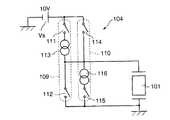
従来、撮影レンズ等が取りつけられた係合部材を棒状の駆動部材に所定の摩擦力を有するように結合させると共に、その駆動部材の一方端に圧電素子を固着して構成されたインパクト型圧電アクチュエータからなる駆動装置が知られている。例えば、図14は、カメラの撮影レンズ位置を調節するための駆動装置の概略構成を示す図である。   2. Description of the Related Art Conventionally, an impact type piezoelectric actuator constructed by coupling an engaging member to which a photographing lens or the like is attached to a rod-like driving member so as to have a predetermined frictional force, and fixing a piezoelectric element to one end of the driving member. A driving device is known. For example, FIG. 14 is a diagram illustrating a schematic configuration of a driving device for adjusting the position of the photographing lens of the camera.

この図における駆動装置100は、電気機械変換素子である圧電素子101と、圧電素子101により駆動される棒状の駆動部材102と、駆動部材102に所定の摩擦力で結合された係合部材103と、圧電素子101に駆動電圧を印加する駆動回路104とを備えている。   The driving device 100 in this figure includes a piezoelectric element 101 that is an electromechanical conversion element, a rod-shaped driving member 102 that is driven by the piezoelectric element 101, and an engagement member 103 that is coupled to the driving member 102 with a predetermined frictional force. And a drive circuit 104 for applying a drive voltage to the piezoelectric element 101.

圧電素子101は、駆動回路104から印加される駆動電圧に応じて伸縮するものであり、その伸縮方向における一方端が支持部材105に固着されると共に、その他方端が駆動部材102の軸方向における一方端に固着されたものである。係合部材103は、所定箇所に駆動対象物である撮影レンズLが固着され、駆動部材102上を軸方向に沿って移動可能とされている。   The piezoelectric element 101 expands and contracts according to the drive voltage applied from the drive circuit 104, and one end in the expansion / contraction direction is fixed to the support member 105, and the other end is in the axial direction of the drive member 102. One is fixed to one end. The engaging member 103 has a photographing lens L, which is a driving object, fixed to a predetermined location, and is movable along the axial direction on the driving member 102.

駆動回路104は、例えば図15に示すように、緩速充電回路及び急速放電回路からなる第1の駆動回路109と、急速充電回路及び緩速放電回路からなる第2の駆動回路110とから構成され、デジタル回路で生成した0〜5Vの矩形波信号により各駆動回路109,110を駆動制御するようにしたものである。   For example, as shown in FIG. 15, the drive circuit 104 includes a first drive circuit 109 composed of a slow charge circuit and a rapid discharge circuit, and a second drive circuit 110 composed of a quick charge circuit and a slow discharge circuit. The drive circuits 109 and 110 are driven and controlled by a rectangular wave signal of 0 to 5 V generated by a digital circuit.

すなわち、第1の駆動回路109は、電源電圧Vpに対して2つのスイッチ111,112と定電流源113とを定電流源113が中間位置にくるようにして直列接続することにより構成され、第2の駆動回路110は、電源電圧Vpに対して2つのスイッチ114,115と定電流源116とを定電流源116が中間位置にくるようにして直列接続することにより構成されたものであり、スイッチ112と定電流源113間及びスイッチ114と定電流源116間の出力が圧電素子101に印加されるようにしたものである。   That is, the first drive circuit 109 is configured by connecting in series the two switches 111 and 112 and the constant current source 113 with respect to the power supply voltage Vp so that the constant current source 113 is at an intermediate position. The second drive circuit 110 is configured by connecting two switches 114 and 115 and a constant current source 116 in series with respect to the power supply voltage Vp so that the constant current source 116 is at an intermediate position. The outputs between the switch 112 and the constant current source 113 and between the switch 114 and the constant current source 116 are applied to the piezoelectric element 101.

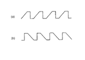
この図15に示す駆動回路104では、第1の駆動回路109のスイッチ111を閉じることにより緩速充電回路が形成され、その後にスイッチ111を開いてスイッチ112を閉じることにより急速放電回路が形成される。このスイッチ操作が矩形波信号により繰り返し実行されることにより、緩慢な立ち上がり部と急峻な立ち下がり部とを有する図16(a)に示すような波形(繰出波形)の駆動電圧が圧電素子101に繰り返し印加され、圧電素子101の伸縮により係合部材103は繰出方向(圧電素子101から離反する方向)である矢印a方向に移動する。   In the drive circuit 104 shown in FIG. 15, a slow charge circuit is formed by closing the switch 111 of the first drive circuit 109, and then a rapid discharge circuit is formed by opening the switch 111 and closing the switch 112. The By repeatedly performing this switch operation with a rectangular wave signal, a drive voltage having a waveform (progress waveform) having a slow rising portion and a steep falling portion as shown in FIG. Repetitively applied, the engagement member 103 moves in the direction of arrow a which is the feeding direction (the direction away from the piezoelectric element 101) due to expansion and contraction of the piezoelectric element 101.

すなわち、駆動電圧の緩慢な立ち上がり部では圧電素子101が緩やかに伸長することになるため、係合部材103は駆動部材102と共に繰出方向に移動する一方、急峻な立ち下がり部では圧電素子101が急激に縮小することになるため、駆動部材102が戻り方向に移動しても係合部材103は駆動部材102上をスリップして略同位置に留まることになる。このため、図16(a)に示すような波形の駆動電圧が圧電素子101に繰り返し印加されると、係合部材103は矢印a方向に間欠的に移動する。   That is, since the piezoelectric element 101 is gently extended at the rising portion where the driving voltage is slow, the engaging member 103 moves in the feeding direction together with the driving member 102, while the piezoelectric element 101 is suddenly moved at the sharp falling portion. Therefore, even if the driving member 102 moves in the return direction, the engaging member 103 slips on the driving member 102 and stays at substantially the same position. For this reason, when a driving voltage having a waveform as shown in FIG. 16A is repeatedly applied to the piezoelectric element 101, the engaging member 103 moves intermittently in the direction of the arrow a.

また、第2の駆動回路110のスイッチ114を閉じることにより急速充電回路が形成され、その後にスイッチ114を開いてスイッチ115を閉じることにより緩速放電回路が形成される。このスイッチ操作が矩形波信号により繰り返し実行されることにより、急峻な立ち上がり部と緩慢な立ち下がり部とを有する図16(b)に示すような波形(戻し波形)の駆動電圧が圧電素子101に繰り返し印加され、圧電素子101の伸縮により係合部材103は戻り方向(圧電素子101に接近する方向)である矢印aとは反対方向に移動する。   Further, the quick charge circuit is formed by closing the switch 114 of the second drive circuit 110, and then the slow discharge circuit is formed by opening the switch 114 and then closing the switch 115. By repeatedly executing this switch operation with a rectangular wave signal, a driving voltage having a waveform (return waveform) as shown in FIG. 16B having a steep rising portion and a slow falling portion is applied to the piezoelectric element 101. Repeatedly applied, the engagement member 103 moves in the direction opposite to the arrow a which is the return direction (direction approaching the piezoelectric element 101) due to expansion and contraction of the piezoelectric element 101.

すなわち、駆動電圧の急峻な立ち上がり部では圧電素子101が急激に伸長することになるため、駆動部材102が繰出方向に移動しても係合部材103は駆動部材102上をスリップして略同位置に留まることになる一方、緩慢な立ち下がり部では圧電素子101が緩やかに縮小することになるため、係合部材103は駆動部材102と共に戻り方向に移動することになる。このため、図16(b)に示すような波形の駆動電圧が圧電素子101に繰り返し印加されると、係合部材103は矢印aとは反対方向に間欠的に移動する。これにより、レンズLが繰出方向と戻り方向とに移動可能となる。   That is, since the piezoelectric element 101 expands suddenly at the steep rising portion of the driving voltage, the engaging member 103 slips on the driving member 102 even when the driving member 102 moves in the feeding direction, and is approximately at the same position. On the other hand, since the piezoelectric element 101 is gradually reduced at the slow falling portion, the engaging member 103 moves together with the driving member 102 in the return direction. For this reason, when a driving voltage having a waveform as shown in FIG. 16B is repeatedly applied to the piezoelectric element 101, the engaging member 103 moves intermittently in the direction opposite to the arrow a. Thereby, the lens L can be moved in the feeding direction and the returning direction.

特開平10−248277号公報Japanese Patent Laid-Open No. 10-248277

ところで、カメラの撮影レンズ等の光学系の駆動源としてインパクト形圧電アクチュエータからなる駆動装置を適用する場合、その駆動装置はできる限り構成が簡素化され、かつ小型化されていることが望ましい。しかしながら、上記従来の駆動装置100では、定電流源113,116の回路構成が複雑になることから駆動回路104が複雑化すると共に、小型化にも制約を受けるという問題があった。   By the way, when applying a driving device composed of an impact type piezoelectric actuator as a driving source of an optical system such as a photographing lens of a camera, it is desirable that the configuration of the driving device be simplified and miniaturized as much as possible. However, the conventional driving device 100 has a problem in that the circuit configuration of the constant current sources 113 and 116 is complicated, so that the driving circuit 104 is complicated and the size is limited.

本発明は、このような事情に鑑みてなされたものであり、駆動回路の複雑化等を招くことのない駆動装置を提供することを目的とする。   The present invention has been made in view of such circumstances, and an object of the present invention is to provide a drive device that does not cause the drive circuit to be complicated.

上記目的を達成するため、本発明の一態様に係る駆動装置は、駆動電圧が印加されることにより伸縮する電気機械変換素子と、該電気機械変換素子により駆動される駆動部材と、該駆動部材に所定の摩擦力で係合され、該駆動部材上を移動する係合部材と、前記電気機械変換素子を駆動する駆動回路と、該駆動回路の動作を制御する駆動制御手段とから構成され、前記電気機械変換素子を異なる速度で伸縮させることで前記電気機械変換素子と前記係合部材とを相対移動させる駆動装置において、前記駆動回路は、前記電気機械変換素子の共振周波数に対して0.3倍より大きく1.5倍より小さい駆動周波数をもつ矩形波からなる駆動電圧を前記電気機械変換素子に印加することで、該駆動電圧が、前記駆動部材と係合部材との係合部分に、前記の伸縮時における速度差を生じさせることができる鋸歯状の変位振動を生じさせるものであることを特徴としている。 In order to achieve the above object, a driving device according to one embodiment of the present invention includes an electromechanical transducer that expands and contracts when a driving voltage is applied, a driving member that is driven by the electromechanical transducer, and the driving member. And an engagement member that moves on the drive member, a drive circuit that drives the electromechanical conversion element, and a drive control means that controls the operation of the drive circuit. In the drive device that moves the electromechanical conversion element and the engagement member relative to each other by expanding and contracting the electromechanical conversion element at different speeds, the drive circuit has a frequency of 0. 0 with respect to the resonance frequency of the electromechanical conversion element. the driving voltage comprising a square wave having a 1.5-fold less than the drive frequency greater than three times that applied to the electromechanical transducer, the drive voltage is, the engaging portion between the drive member and the engagement member It is characterized in that to produce a sawtooth displacements vibrations can produce a speed difference at the time of the expansion and contraction.

この構成によれば、共振系における電気機械変換素子の共振周波数の影響を受けて矩形波を形成している高周波成分のうち3次以上の高次の高周波のゲインが大きく減衰し、電気機械変換素子の変位波形が鋸歯形状となる。このため、従来のような定電流源が不要となり、駆動回路の複雑化等を招くことのない駆動装置が実現される。   According to this configuration, the high-frequency gain of the third or higher order among the high-frequency components forming the rectangular wave under the influence of the resonance frequency of the electromechanical conversion element in the resonance system is greatly attenuated, and the electromechanical conversion The displacement waveform of the element has a sawtooth shape. This eliminates the need for a constant current source as in the prior art, and realizes a drive device that does not cause complication of the drive circuit.

また、他の一態様では、上述の駆動装置において、前記駆動回路は、前記電気機械変換素子にその一方側から駆動電圧を印加して充電する第1の駆動回路と、前記電気機械変換素子にその他方側から駆動電圧を印加して充電する第2の駆動回路と、各駆動回路により電気機械変換素子に充電された電荷を放電する放電回路とを備え、前記駆動制御手段は、前記第1の駆動回路と第2の駆動回路とを交互に駆動させると共に、前記第1の駆動回路の駆動期間と第2の駆動回路の駆動期間との間に前記放電回路を駆動するようにしたことを特徴としている。   According to another aspect, in the above-described driving device, the driving circuit applies a driving voltage to the electromechanical conversion element from one side and charges the electromechanical conversion element, and the electromechanical conversion element. A second drive circuit for charging by applying a drive voltage from the other side; and a discharge circuit for discharging the charge charged in the electromechanical conversion element by each drive circuit, wherein the drive control means includes the first drive circuit The driving circuit and the second driving circuit are alternately driven, and the discharge circuit is driven between the driving period of the first driving circuit and the driving period of the second driving circuit. It is a feature.

この構成によれば、第1の駆動回路により電気機械変換素子に充電された電荷は、第2の駆動回路により電気機械変換素子に逆方向に充電される前に放電回路により放電される。また、第2の駆動回路により電気機械変換素子に逆方向に充電された電荷は、第1の駆動回路により電気機械変換素子が充電される前に放電回路により放電される。このため、駆動回路の複雑化等を招くことがないことに加え、消費電力を可及的に抑制して電池電源で有効に駆動することができる駆動装置が実現される。   According to this configuration, the charge charged in the electromechanical conversion element by the first drive circuit is discharged by the discharge circuit before being charged in the reverse direction by the second drive circuit. In addition, the charge charged in the reverse direction to the electromechanical conversion element by the second drive circuit is discharged by the discharge circuit before the electromechanical conversion element is charged by the first drive circuit. For this reason, in addition to not complicating the drive circuit, etc., a drive device that can be effectively driven by the battery power source while suppressing power consumption as much as possible is realized.

また、他の一態様では、上述の駆動装置において、前記第1の駆動回路は、一方端が電源に接続され、他方端が前記電気機械変換素子の一方端に接続されてなる第1のスイッチ手段と、一方端が前記電気機械変換素子の他方端に接続され、他方端が接地されてなる第2のスイッチ手段とで構成されると共に、前記第2の駆動回路は、一方端が前記電源に接続され、他方端が前記電気機械変換素子の他方端に接続されてなる第3のスイッチ手段と、一方端が前記電気機械変換素子の一方端に接続され、他方端が接地されてなる第4のスイッチ手段とで構成され、前記放電回路は、前記第2のスイッチ手段と第4のスイッチ手段とで構成されていることを特徴としている。   According to another aspect, in the above drive device, the first drive circuit includes a first switch having one end connected to a power source and the other end connected to one end of the electromechanical transducer. And second switch means having one end connected to the other end of the electromechanical transducer and the other end grounded, and the second drive circuit has one end connected to the power source. A third switch means having the other end connected to the other end of the electromechanical transducer, and one end connected to one end of the electromechanical transducer and the other end grounded. 4, and the discharge circuit is constituted by the second switch means and the fourth switch means.

この構成によれば、第1のスイッチ手段と第2のスイッチ手段とで構成される第1の駆動回路により電気機械変換素子に充電された電荷は、第2の駆動回路により電気機械変換素子に逆方向に充電される前に第2のスイッチ手段と第4のスイッチ手段とで構成される放電回路により放電される。また、第3のスイッチ手段と第4のスイッチ手段とで構成される第2の駆動回路により電気機械変換素子に逆方向に充電された電荷は、第1のスイッチ手段と第2のスイッチ手段とで構成される第1の駆動回路により電気機械変換素子が充電される前に第2のスイッチ手段と第4のスイッチ手段とで構成される放電回路により放電される。このため、駆動回路の複雑化等を招くことないことに加え、消費電力を可及的に抑制して電池電源で有効に駆動することができる駆動装置が実現される。   According to this configuration, the charge charged in the electromechanical conversion element by the first drive circuit configured by the first switch means and the second switch means is transferred to the electromechanical conversion element by the second drive circuit. Before being charged in the reverse direction, the battery is discharged by a discharge circuit composed of the second switch means and the fourth switch means. The charge charged in the reverse direction to the electromechanical conversion element by the second drive circuit constituted by the third switch means and the fourth switch means is the first switch means and the second switch means. Before the electromechanical conversion element is charged by the first drive circuit configured as described above, it is discharged by the discharge circuit configured by the second switch means and the fourth switch means. For this reason, in addition to not complicating the drive circuit and the like, a drive device that can be effectively driven by the battery power supply while suppressing power consumption as much as possible is realized.

以上説明したように、本発明の一態様に係る駆動装置によれば、駆動回路は、電気機械変換素子の共振周波数に対して0.3倍より大きく1.5倍より小さい駆動周波数をもつ矩形波からなる駆動電圧を電気機械変換素子に印加するものであるので、駆動回路の複雑化等を招くことがないものとなる。   As described above, according to the driving device of one embodiment of the present invention, the driving circuit has a rectangular shape having a driving frequency that is greater than 0.3 times and smaller than 1.5 times the resonance frequency of the electromechanical transducer. Since a drive voltage composed of waves is applied to the electromechanical conversion element, the drive circuit is not complicated.

また、他の態様の駆動装置によれば、駆動回路は、電気機械変換素子にその一方側から駆動電圧を印加して充電する第1の駆動回路と、電気機械変換素子にその他方側から駆動電圧を印加して充電する第2の駆動回路と、各駆動回路により電気機械変換素子に充電された電荷を放電する放電回路とを備え、駆動制御手段は、第1の駆動回路と第2の駆動回路とを交互に駆動させると共に、第1の駆動回路の駆動期間と第2の駆動回路の駆動期間との間に放電回路を駆動するようにしているので、駆動回路の複雑化等を招くことないことに加え、消費電力を可及的に抑制して電池電源で有効に駆動することができるようになる。   According to another aspect of the drive device, the drive circuit is driven by applying a drive voltage to the electromechanical conversion element from one side and charging the electromechanical conversion element from the other side. A second drive circuit for charging by applying a voltage; and a discharge circuit for discharging the charge charged in the electromechanical transducer by each drive circuit. The drive control means includes the first drive circuit, the second drive circuit, and the second drive circuit. Since the driving circuit is driven alternately and the discharge circuit is driven between the driving period of the first driving circuit and the driving period of the second driving circuit, the driving circuit is complicated. In addition to this, power consumption can be suppressed as much as possible, and the battery can be driven effectively.

また、他の態様の駆動装置によれば、第1の駆動回路は、一方端が電源に接続され、他方端が電気機械変換素子の一方端に接続されてなる第1のスイッチ手段と、一方端が電気機械変換素子の他方端に接続され、他方端が接地されてなる第2のスイッチ手段とで構成されると共に、第2の駆動回路は、一方端が電源に接続され、他方端が電気機械変換素子の他方端に接続されてなる第3のスイッチ手段と、一方端が電気機械変換素子の一方端に接続され、他方端が接地されてなる第4のスイッチ手段とで構成され、放電回路は、第2のスイッチ手段と第4のスイッチ手段とで構成されているので、簡単な回路構成で駆動回路を構成することができる。   According to another aspect of the drive device, the first drive circuit includes a first switch means having one end connected to the power source and the other end connected to one end of the electromechanical transducer, The second drive circuit has one end connected to the power source and the other end connected to the power source, the second switch circuit having the other end connected to the other end of the electromechanical transducer and the other end grounded. A third switch means connected to the other end of the electromechanical conversion element; and a fourth switch means having one end connected to one end of the electromechanical conversion element and the other end grounded; Since the discharge circuit is composed of the second switch means and the fourth switch means, the drive circuit can be configured with a simple circuit configuration.

本発明の一実施形態に係る駆動装置の構成を概略的に示す図である。It is a figure which shows schematically the structure of the drive device which concerns on one Embodiment of this invention. 図1に示す駆動装置の駆動部の構成例を示す斜視図である。It is a perspective view which shows the structural example of the drive part of the drive device shown in FIG. 図1に示す駆動装置の駆動回路の構成例を示す図である。It is a figure which shows the structural example of the drive circuit of the drive device shown in FIG. 図3に示す駆動回路により圧電素子に印加される駆動パルスの波形を示す図で、(a)はデューティ比が0.3になるように設定されたもの、(b)はデューティ比が0.7になるように設定されたものである。FIGS. 4A and 4B are diagrams showing waveforms of drive pulses applied to the piezoelectric element by the drive circuit shown in FIG. 3, in which FIG. 3A is set so that the duty ratio is 0.3, and FIG. 7 is set to be 7. 図1に示す駆動装置におけるfd/frと係合部材の移動速度との関係を示す図である。It is a figure which shows the relationship between fd / fr and the moving speed of an engaging member in the drive device shown in FIG. 図1に示す駆動装置における駆動電圧のデューティ比と係合部材の移動速度との関係を示す図である。It is a figure which shows the relationship between the duty ratio of the drive voltage in the drive device shown in FIG. 1, and the moving speed of an engaging member. 図1に示す駆動装置における圧電素子に印加される駆動電圧と、圧電素子の伸縮による変位波形との関係を示す図で、(a)は駆動電圧のデューティ比が0.3になるように設定された場合のもの、(b)は駆動電圧のデューティ比が0.7になるように設定された場合のものである。FIG. 2 is a diagram showing a relationship between a driving voltage applied to a piezoelectric element in the driving apparatus shown in FIG. 1 and a displacement waveform due to expansion and contraction of the piezoelectric element, and FIG. (B) shows the case where the duty ratio of the drive voltage is set to be 0.7. 図3に示す駆動回路を制御する制御回路から出力されて各スイッチ素子に印加される駆動パルスと、圧電素子に印加される駆動電圧の波形とを示す図である。It is a figure which shows the waveform of the drive pulse which is output from the control circuit which controls the drive circuit shown in FIG. 3, and is applied to each switch element, and the drive voltage applied to a piezoelectric element. 図3に示す駆動回路の各スイッチ素子の動作を説明するための図である。FIG. 4 is a diagram for explaining the operation of each switch element of the drive circuit shown in FIG. 3. 図3に示す駆動回路の効果を説明するための図であり、(a)は消費電力、(b)は係合部材の移動速度を示すグラフである。4A and 4B are diagrams for explaining the effect of the drive circuit shown in FIG. 3, in which FIG. 図1に示す駆動装置の駆動回路の別の構成例を示すブロック図である。It is a block diagram which shows another structural example of the drive circuit of the drive device shown in FIG. 図11に示す駆動回路を制御する制御回路から出力されて各スイッチ素子に印加される駆動パルスと、圧電素子に印加される駆動電圧の波形とを示す図である。It is a figure which shows the waveform of the drive pulse which is output from the control circuit which controls the drive circuit shown in FIG. 11, and is applied to each switch element, and the drive voltage applied to a piezoelectric element. 図1に示す駆動部の別の構成例を示す図で、(a)はその分解斜視図、(b)はその正面図である。It is a figure which shows another structural example of the drive part shown in FIG. 1, (a) is the disassembled perspective view, (b) is the front view. 従来例の駆動装置の構成を概略的に示す図である。It is a figure which shows schematically the structure of the drive device of a prior art example. 図14に示す駆動装置の駆動回路の構成例を示すブロック図である。FIG. 15 is a block diagram illustrating a configuration example of a drive circuit of the drive device illustrated in FIG. 14. 図14に示す駆動回路の出力波形を示す図で、(a)は繰出波形、(b)は戻り波形である。FIGS. 15A and 15B are diagrams showing output waveforms of the drive circuit shown in FIG. 14, where FIG.

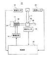
図1は、本発明の一実施形態に係るインパクト型圧電アクチュエータからなる駆動装置の基本構成を概略的に示すブロック図である。この図において、駆動装置10は、駆動部12と、駆動部12を駆動する駆動回路14と、駆動部12に取り付けられている係合部材の位置を検出する部材センサ16と、駆動部12の基端に配設された基端センサ18と、駆動部12の先端に配設された先端センサ20と、全体の動作を制御する制御部22とを備えている。   FIG. 1 is a block diagram schematically showing a basic configuration of a drive device including an impact type piezoelectric actuator according to an embodiment of the present invention. In this figure, the drive device 10 includes a drive unit 12, a drive circuit 14 that drives the drive unit 12, a member sensor 16 that detects the position of an engagement member attached to the drive unit 12, and the drive unit 12. A proximal sensor 18 disposed at the proximal end, a distal sensor 20 disposed at the distal end of the drive unit 12, and a control unit 22 for controlling the overall operation are provided.

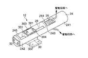
図2は、駆動部12の構成例を示す斜視図である。この図において、駆動部12は、素子固定式構造のものであり、支持部材24、圧電素子26、駆動部材28及び係合部材30から構成されている。   FIG. 2 is a perspective view illustrating a configuration example of the drive unit 12. In this figure, the drive unit 12 has an element-fixed structure, and includes a support member 24, a piezoelectric element 26, a drive member 28, and an engagement member 30.

支持部材24は、圧電素子26及び駆動部材28を保持するものであり、円柱体の軸方向両端部241,242及び略中央の仕切壁243を残して内部を刳り貫くことにより形成された第1の収容空間244及び第2の収容空間245を有している。この第1の収容空間244には、圧電素子26がその分極方向である伸縮方向を支持部材24の軸方向と一致させて収容されている。また、第2の収容空間245には、駆動部材28と係合部材30の一部とが収容されている。   The support member 24 holds the piezoelectric element 26 and the drive member 28, and is formed by scoring the inside leaving the axial both ends 241 and 242 and the substantially central partition wall 243. Storage space 244 and second storage space 245. In the first accommodation space 244, the piezoelectric element 26 is accommodated so that the expansion / contraction direction, which is the polarization direction, coincides with the axial direction of the support member 24. Further, the drive member 28 and a part of the engagement member 30 are accommodated in the second accommodation space 245.

圧電素子26は、例えば、所要の厚みを有する複数枚の圧電基板を各圧電基板間に図略の電極を介して積層することにより構成したものであり、その伸縮方向(積層方向)である長手方向の一方端面が第1の収容空間244の一方端部241側端面に固着されている。支持部材24の他方端部242及び仕切壁243には中心位置に丸孔が穿設されると共に、この両丸孔を貫通して断面丸形状の棒状の駆動部材28が第2収容空間245に軸方向に沿って移動可能に収容されている。   The piezoelectric element 26 is formed by, for example, laminating a plurality of piezoelectric substrates having a required thickness between each piezoelectric substrate via an unillustrated electrode, and a longitudinal direction that is an expansion / contraction direction (lamination direction). One end surface in the direction is fixed to the one end portion 241 side end surface of the first accommodation space 244. The other end 242 of the support member 24 and the partition wall 243 are provided with a round hole at the center position, and a rod-shaped drive member 28 having a round cross section passes through the round holes in the second housing space 245. It is accommodated so as to be movable along the axial direction.

駆動部材28の第1の収容空間244内に突出した端部は圧電素子26の他方端面に固着され、駆動部材28の第2の収容空間245の外部に突出した端部は板ばね32により所要のばね圧で圧電素子26側に付勢されている。この板ばね32による駆動部材28への付勢は、圧電素子26の伸縮動作に基づく駆動部材28の軸方向変位を安定化させるためである。   The end of the driving member 28 protruding into the first housing space 244 is fixed to the other end surface of the piezoelectric element 26, and the end of the driving member 28 protruding outside the second housing space 245 is required by the leaf spring 32. Is biased toward the piezoelectric element 26 by the spring pressure. The urging of the drive member 28 by the leaf spring 32 is to stabilize the axial displacement of the drive member 28 based on the expansion / contraction operation of the piezoelectric element 26.

係合部材30は、駆動部材28の軸方向の両側に取付部301を有する基部302と、両取付部301の間に装着される挟み込み部材303とを備えており、基部302が駆動部材28に遊嵌されると共に、挟み込み部材303が板ばね304により押圧されることにより駆動部材28に接触することで係合部材30が所定の摩擦力で駆動部材28に結合され、係合部材30に対してその摩擦力よりも大きな駆動力が作用したときに駆動部材28の軸方向に沿って移動可能とされている。なお、係合部材30には駆動対象物であるレンズL(図1)が取り付けられている。   The engaging member 30 includes a base portion 302 having mounting portions 301 on both sides in the axial direction of the drive member 28, and a sandwiching member 303 mounted between the mounting portions 301. The base portion 302 is attached to the driving member 28. The engagement member 30 is coupled to the drive member 28 with a predetermined frictional force when the sandwiching member 303 is pressed by the leaf spring 304 and is brought into contact with the drive member 28 while being loosely fitted. When a driving force larger than the frictional force is applied, the driving member 28 can move along the axial direction. Note that a lens L (FIG. 1) that is a driving object is attached to the engaging member 30.

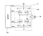
図3は、駆動回路14の構成例を示す図である。この図において、駆動回路14は、図略の駆動電源から駆動電圧+Vpが供給される接続点aと、接地される接続点bとの間に、MOS型FETであるスイッチ素子Q1からなる第1スイッチ回路141及びMOS型FETであるスイッチ素子Q2からなる第2スイッチ回路142の直列回路が接続されると共に、MOS型FETであるスイッチ素子Q3からなる第3スイッチ回路143及びMOS型FETであるスイッチ素子Q4からなる第4スイッチ回路144の直列回路が接続され、各スイッチ回路141乃至144に駆動制御信号Sc1,Sc2,Sc3,Sc4を供給する制御信号供給手段としての制御回路145が接続されて構成されている。   FIG. 3 is a diagram illustrating a configuration example of the drive circuit 14. In this figure, the drive circuit 14 includes a first switch element Q1 which is a MOS FET between a connection point a to which a drive voltage + Vp is supplied from a drive power supply (not shown) and a connection point b to be grounded. A series circuit of a switch circuit 141 and a second switch circuit 142 composed of a switch element Q2 which is a MOS type FET is connected, and a third switch circuit 143 composed of a switch element Q3 which is a MOS type FET and a switch which is a MOS type FET. A series circuit of a fourth switch circuit 144 composed of an element Q4 is connected, and a control circuit 145 is connected as a control signal supply means for supplying drive control signals Sc1, Sc2, Sc3, Sc4 to the switch circuits 141 to 144. Has been.

第1スイッチ回路141を構成するスイッチ素子Q1及び第3スイッチ回路143を構成するスイッチ素子Q3はPチャネルFETであり、第2スイッチ回路142を構成するスイッチ素子Q2及び第4スイッチ回路144を構成するスイッチ素子Q4はNチャネルFETである。PチャネルFETであるスイッチ素子Q1,Q3は駆動制御信号がローレベルのときにオンになり、NチャネルFETであるスイッチ素子Q2,Q4は駆動制御信号がハイレベルのときにオンになる。なお、第1スイッチ回路141及び第2スイッチ回路142の接続点cと、第3スイッチ回路143及び第4スイッチ回路144の接続点dとの間に圧電素子26が接続されてブリッジ回路146が構成されている。   The switch element Q1 constituting the first switch circuit 141 and the switch element Q3 constituting the third switch circuit 143 are P-channel FETs, and constitute the switch element Q2 and the fourth switch circuit 144 constituting the second switch circuit 142. The switch element Q4 is an N-channel FET. The switch elements Q1 and Q3 that are P-channel FETs are turned on when the drive control signal is at a low level, and the switch elements Q2 and Q4 that are N-channel FETs are turned on when the drive control signal is at a high level. The bridge circuit 146 is configured by connecting the piezoelectric element 26 between the connection point c of the first switch circuit 141 and the second switch circuit 142 and the connection point d of the third switch circuit 143 and the fourth switch circuit 144. Has been.

このように構成された駆動回路14において、第1スイッチ回路141及び第4スイッチ回路144は圧電素子26に対し、その一方側から駆動電圧+Vpを印加して端子間電圧Vsが+Vpとなるまで充電する第1の駆動回路(第1の駆動手段)を構成し、第2スイッチ回路142及び第3スイッチ回路143は圧電素子26に対し、その他方側から(すなわち、逆方向から)駆動電圧+Vpを印加して端子間電圧Vsが−Vpとなるまで充電する第2の駆動回路(第2の駆動手段)を構成することになる。   In the drive circuit 14 configured as above, the first switch circuit 141 and the fourth switch circuit 144 are charged until the drive voltage + Vp is applied to the piezoelectric element 26 from one side until the inter-terminal voltage Vs becomes + Vp. The second switch circuit 142 and the third switch circuit 143 apply the drive voltage + Vp to the piezoelectric element 26 from the other side (that is, from the reverse direction). A second drive circuit (second drive means) is configured to be applied and charged until the inter-terminal voltage Vs becomes −Vp.

このように駆動回路14と圧電素子26とでブリッジ回路146を構成した場合、圧電素子26には−Vp〜+Vpの電圧が印加されるので、圧電素子26の駆動電圧が等価的に2Vpとなる結果、駆動電源は低電圧であっても変位量の大きい駆動装置10を得ることができるという利点がある。   When the bridge circuit 146 is configured by the drive circuit 14 and the piezoelectric element 26 as described above, a voltage of −Vp to + Vp is applied to the piezoelectric element 26, so that the drive voltage of the piezoelectric element 26 is equivalently 2 Vp. As a result, there is an advantage that the driving device 10 having a large amount of displacement can be obtained even when the driving power source is at a low voltage.

図1に戻り、部材センサ16は、係合部材30の移動可能範囲内に配設されており、MRE(Magneto Resistive Effect)素子やPSD(Position Sensitive Device)素子等
のセンサにより構成されている。また、基端センサ18及び先端センサ20は、フォトインタラプタ等のセンサにより構成されている。これにより、係合部材30の位置が部材センサ16により検出されることで係合部材30の所定位置への移動制御が可能となる一方、係合部材30の位置が基端センサ18及び先端センサ20で検出されることで係合部材30のそれ以上の移動が禁止される。
Returning to FIG. 1, the member sensor 16 is disposed within a movable range of the engaging member 30, and includes a sensor such as an MRE (Magneto Resistive Effect) element or a PSD (Position Sensitive Device) element. In addition, the proximal sensor 18 and the distal sensor 20 are configured by sensors such as a photo interrupter. Thus, the position of the engaging member 30 is detected by the member sensor 16 so that the movement of the engaging member 30 to a predetermined position can be controlled. On the other hand, the position of the engaging member 30 is determined by the proximal sensor 18 and the distal sensor. By detecting at 20, the further movement of the engaging member 30 is prohibited.

制御部22は、演算処理を行うCPU(Central Processing Unit)、処理プログラム
及びデータが記憶されたROM(Read-Only Memory)及びデータを一時的に記憶するRAM(Random Access Memory)から構成されており、部材センサ16等から入力される信号に基づいて制御回路145から所定のデューティ比の駆動パルスを出力させ、この駆動パルスにより第1の駆動回路及び第2の駆動回路を交互に駆動する。すなわち、制御部22は、第1スイッチ回路141及び第4スイッチ回路144からなる第1の駆動回路と、第2スイッチ回路142及び第3スイッチ回路143からなる第2の駆動回路とを交互に駆動する一方、後述する第2スイッチ回路142及び第4スイッチ回路144からなる放電回路を駆動する駆動制御手段を構成する。
The control unit 22 includes a CPU (Central Processing Unit) that performs arithmetic processing, a ROM (Read-Only Memory) that stores processing programs and data, and a RAM (Random Access Memory) that temporarily stores data. Based on a signal input from the member sensor 16 or the like, a drive pulse having a predetermined duty ratio is output from the control circuit 145, and the first drive circuit and the second drive circuit are alternately driven by the drive pulse. That is, the control unit 22 alternately drives the first drive circuit composed of the first switch circuit 141 and the fourth switch circuit 144 and the second drive circuit composed of the second switch circuit 142 and the third switch circuit 143. On the other hand, drive control means for driving a discharge circuit composed of a second switch circuit 142 and a fourth switch circuit 144 described later is configured.

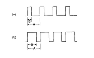
次に、本発明の駆動装置10に適用される駆動回路14の駆動動作の説明を行うに先立ち、図4乃至図7を参照して駆動回路14の原理的な動作説明を行う。すなわち、図4は、駆動回路14の原理的な動作を説明するための駆動電圧のパルス波形を示す図であり、同図(a)は駆動電圧の駆動周波数fdが支持部材24及び駆動部材28が固着された状態での圧電素子26の共振周波数frの0.7倍(fd=0.7×fr)となるように設定され、デューティ比D(D=B/A)が0.3になるように設定されたもの、同図(b)は駆動電圧の駆動周波数fdが支持部材24及び駆動部材28が固着された状態での圧電素子26の共振周波数frの0.7倍(fd=0.7×fr)となるように設定され、デューティ比D(D=B/A)が0.7になるように設定されたものである。   Next, prior to the description of the drive operation of the drive circuit 14 applied to the drive device 10 of the present invention, the principle operation of the drive circuit 14 will be described with reference to FIGS. That is, FIG. 4 is a diagram showing a pulse waveform of the drive voltage for explaining the principle operation of the drive circuit 14. FIG. 4A shows the drive frequency fd of the drive voltage with the support member 24 and the drive member 28. Is set to be 0.7 times the resonant frequency fr of the piezoelectric element 26 in a state where is fixed (fd = 0.7 × fr), and the duty ratio D (D = B / A) is set to 0.3. In FIG. 5B, the drive frequency fd of the drive voltage is 0.7 times the resonance frequency fr of the piezoelectric element 26 with the support member 24 and the drive member 28 fixed (fd = 0.7 × fr), and the duty ratio D (D = B / A) is set to 0.7.

このように、図4(a)に示す矩形波からなる駆動電圧が圧電素子26に印加された場合は係合部材30が駆動部材28に沿って繰出方向(圧電素子26から離反する方向)である矢印a方向に移動し、図4(b)に示す矩形波からなる駆動電圧が圧電素子26に印加された場合は係合部材30が駆動部材28に沿って戻り方向(圧電素子26に接近する方向)である矢印aとは逆方向に移動することになる。駆動電圧をこのように設定したのは、支持部材24及び駆動部材28が固着されている状態での圧電素子26の共振周波数frに対する駆動電圧の周波数fdの比(fd/fr)と係合部材30の移動速度との関係を確認した結果、図5に示すような関係にあることが明らかとなったことによる。   As described above, when the driving voltage composed of the rectangular wave shown in FIG. 4A is applied to the piezoelectric element 26, the engaging member 30 extends along the driving member 28 in the feeding direction (direction away from the piezoelectric element 26). When the drive voltage consisting of a rectangular wave shown in FIG. 4B is applied to the piezoelectric element 26, the engagement member 30 moves along the drive member 28 in the return direction (approaching the piezoelectric element 26). The direction of the arrow a is the opposite direction. The drive voltage is set in this way because the ratio (fd / fr) of the frequency fd of the drive voltage to the resonance frequency fr of the piezoelectric element 26 in a state where the support member 24 and the drive member 28 are fixed and the engagement member. As a result of confirming the relationship with the moving speed of 30, it became clear that the relationship shown in FIG. 5 was obtained.

すなわち、従来では、鋸歯形状の波形を有する駆動電圧が印加された場合に圧電素子26が駆動するものと考えられていたため、その駆動回路が不可避的に複雑となり、低コスト化と小型化とに制約を受けるという問題があったが、本発明に係る駆動装置10の駆動回路14では、上記のように駆動電圧が生成の容易な矩形波からなるものでよいことから低コスト化と小型化とが促進されるという利点がある。   That is, in the past, it was considered that the piezoelectric element 26 is driven when a drive voltage having a sawtooth waveform is applied, so that the drive circuit is inevitably complicated, resulting in cost reduction and size reduction. Although there was a problem of being restricted, in the drive circuit 14 of the drive device 10 according to the present invention, as described above, the drive voltage may be formed of a rectangular wave that can be easily generated. Has the advantage of being promoted.

この図5に示す特性図は、矩形波からなる駆動電圧のデューティ比が0.3の場合(係合部材30が繰出方向に移動する場合)のものであるが、そのデューティ比が0.7の場合(係合部材30が戻り方向に移動する場合)は勿論のこと、そのデューティ比が0.05〜0.95の範囲内にある場合には略同様の関係を有することが確認されている。   The characteristic diagram shown in FIG. 5 is for the case where the duty ratio of the drive voltage composed of a rectangular wave is 0.3 (when the engagement member 30 moves in the feeding direction), and the duty ratio is 0.7. In this case (when the engagement member 30 moves in the return direction), it is confirmed that when the duty ratio is in the range of 0.05 to 0.95, the relationship is substantially the same. Yes.

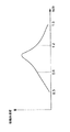
この図5に示す特性図からも明らかなように、fd/frの値が0.3乃至1.5の範囲内にある場合には係合部材30が実質的に移動可能となり、fd/frの値が0.3に満たない場合及び1.5を超える場合には係合部材30が移動不能となる。従って、圧電素子26の共振周波数frに対する駆動電圧の周波数fdは、図4に示すものだけではなく必要に応じて0.3<fd<1.5の範囲内で適宜設定することができる。   As is apparent from the characteristic diagram shown in FIG. 5, when the value of fd / fr is in the range of 0.3 to 1.5, the engaging member 30 is substantially movable, and fd / fr When the value of is less than 0.3 and exceeds 1.5, the engaging member 30 becomes immovable. Therefore, the frequency fd of the drive voltage with respect to the resonance frequency fr of the piezoelectric element 26 can be set as appropriate within the range of 0.3 <fd <1.5 as required, as well as that shown in FIG.

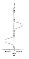
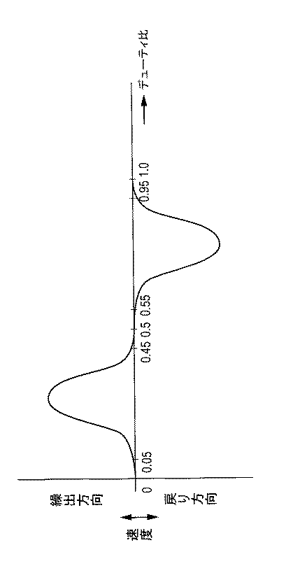
また、矩形波からなる駆動電圧のデューティ比と係合部材30の移動方向(繰出方向及び戻り方向)との関係を確認した結果、図6に示すような関係を有していることが明らかとなっている。すなわち、デューティ比Dが0.05乃至0.45の範囲内(0.05<D<0.45)にあるときには、係合部材30は繰出方向に移動し、デューティ比Dが0.55乃至0.95の範囲内(0.55<D<0.95)にあるときには、係合部材30は戻り方向に移動する。従って、デューティ比Dは、図4に示すものだけではなく必要に応じて0.05<D<0.45又は0.55<D<0.95の範囲内で適宜設定することができる。   Further, as a result of confirming the relationship between the duty ratio of the drive voltage composed of a rectangular wave and the moving direction (feeding direction and returning direction) of the engaging member 30, it is clear that the relationship shown in FIG. It has become. That is, when the duty ratio D is in the range of 0.05 to 0.45 (0.05 <D <0.45), the engagement member 30 moves in the feeding direction, and the duty ratio D is 0.55 to When it is within the range of 0.95 (0.55 <D <0.95), the engagement member 30 moves in the return direction. Therefore, the duty ratio D can be appropriately set within the range of 0.05 <D <0.45 or 0.55 <D <0.95 as required, as well as that shown in FIG.

なお、支持部材24及び駆動部材28が固着された状態での圧電素子26の共振周波数frは、次の数1により求めたものである。   The resonance frequency fr of the piezoelectric element 26 in a state where the support member 24 and the drive member 28 are fixed is obtained by the following equation (1).

Figure 0004666100
Figure 0004666100

この数1におけるfroは圧電素子26の両電極間におけるフリー共振周波数(圧電素子26自体の電極間方向における共振周波数)、mpは圧電素子26の質量、mfは駆動部材28の質量をそれぞれ表わしている。なお、支持部材24の質量は、共振系における圧電素子26の共振周波数frに関係するが、支持部材24の質量は圧電素子26及び駆動部材28の各質量を加算したものに比べて十分大きな値を有しており、共振周波数frに与える影響は小さいので演算パラメータとして考慮する必要はない。また、係合部材30は、圧電素子26の共振時には駆動部材28に対して滑りを生じて実質的に共振系の要素として考慮する必要はないので、上記数1の演算パラメータとしては含まれていない。   In Equation 1, fro represents the free resonance frequency between the electrodes of the piezoelectric element 26 (resonance frequency in the direction between the electrodes of the piezoelectric element 26 itself), mp represents the mass of the piezoelectric element 26, and mf represents the mass of the driving member 28. Yes. The mass of the support member 24 is related to the resonance frequency fr of the piezoelectric element 26 in the resonance system, but the mass of the support member 24 is sufficiently larger than the sum of the masses of the piezoelectric element 26 and the drive member 28. Therefore, the influence on the resonance frequency fr is small, so there is no need to consider it as a calculation parameter. Further, the engaging member 30 does not have to be considered as a substantially resonant element because it slips with respect to the driving member 28 at the time of resonance of the piezoelectric element 26, and is therefore included as the calculation parameter of the above equation (1). Absent.

図7は、圧電素子26に印加される駆動回路14からの駆動電圧のパルス波形と、圧電素子26の伸縮による変位との対応関係を示す図で、同図(a)は図4(a)に示す駆動電圧が印加された場合であり、同図(b)は図4(b)に示す駆動電圧が印加された場合をそれぞれ示している。なお、圧電素子26の伸縮による変位は、レーザードップラー振動計により測定したものである。   FIG. 7 is a diagram showing a correspondence relationship between the pulse waveform of the driving voltage applied from the driving circuit 14 applied to the piezoelectric element 26 and the displacement due to the expansion and contraction of the piezoelectric element 26. FIG. (B) shows the case where the drive voltage shown in FIG. 4 (b) is applied. The displacement due to expansion and contraction of the piezoelectric element 26 is measured by a laser Doppler vibrometer.

このように、圧電素子26に図4(a)に示す駆動電圧が印加された場合は圧電素子26の変位波形が緩慢な立ち上がり部と急峻な立ち下がり部とを有する鋸歯形状となり、圧電素子26に図4(b)に示す駆動電圧が印加された場合は圧電素子26の変位波形が急峻な立ち上がり部と緩慢な立ち下がり部とを有する鋸歯形状となっていることが確認された。   As described above, when the driving voltage shown in FIG. 4A is applied to the piezoelectric element 26, the displacement waveform of the piezoelectric element 26 has a sawtooth shape having a slow rising portion and a steep falling portion. When the drive voltage shown in FIG. 4B is applied, it was confirmed that the displacement waveform of the piezoelectric element 26 has a sawtooth shape having a steep rising portion and a slow falling portion.

すなわち、圧電素子26の変位が図7(a)に示すような緩慢な立ち上がり部を有する波形を呈するとき(すなわち、圧電素子26が緩やかに伸長するとき)は、係合部材30が駆動部材28と共に繰出方向に移動し、圧電素子26の変位が図7(a)に示すような急峻な立下り部を有する波形を呈するとき(すなわち、圧電素子26が急激に縮小するとき)は、駆動部材28が戻り方向に移動しても係合部材30は駆動部材28上をスリップして略同位置に留まることになる。このため、図7(a)に示す駆動電圧が圧電素子26に繰り返し印加されることで、係合部材30は繰出方向に間欠的に移動することになる。   That is, when the displacement of the piezoelectric element 26 exhibits a waveform having a slow rising portion as shown in FIG. 7A (that is, when the piezoelectric element 26 is gently extended), the engaging member 30 is driven by the drive member 28. When the displacement of the piezoelectric element 26 exhibits a waveform having a steep falling portion as shown in FIG. 7A (that is, when the piezoelectric element 26 rapidly shrinks), the drive member Even if 28 moves in the return direction, the engaging member 30 slips on the driving member 28 and stays at substantially the same position. For this reason, when the driving voltage shown in FIG. 7A is repeatedly applied to the piezoelectric element 26, the engaging member 30 moves intermittently in the feeding direction.

また、圧電素子26の変位が図7(b)に示すような急峻な立ち上がり部を有する波形を呈するとき(すなわち、圧電素子26が急激に伸長するとき)は、駆動部材28が繰出方向に移動しても係合部材30は駆動部材28上をスリップして略同位置に留まることになり、圧電素子26の変位が図7(b)に示すような緩慢な立下り部を有する波形を呈するとき(すなわち、圧電素子26が緩やかに縮小するとき)は、係合部材30が駆動部材28と共に戻り方向に移動することになる。このため、図7(b)に示す駆動電圧が圧電素子26に繰り返し印加されることで、係合部材30は戻り方向に間欠的に移動することになる。   Further, when the displacement of the piezoelectric element 26 exhibits a waveform having a steep rising portion as shown in FIG. 7B (that is, when the piezoelectric element 26 expands rapidly), the driving member 28 moves in the feeding direction. Even so, the engaging member 30 slips on the driving member 28 and stays at substantially the same position, and the displacement of the piezoelectric element 26 exhibits a waveform having a slow falling portion as shown in FIG. At that time (that is, when the piezoelectric element 26 is gradually reduced), the engagement member 30 moves in the return direction together with the drive member 28. For this reason, when the driving voltage shown in FIG. 7B is repeatedly applied to the piezoelectric element 26, the engaging member 30 moves intermittently in the return direction.

このように、例えば、図4(a),(b)に示す駆動電圧が圧電素子26に印加された場合、圧電素子26の変位波形が鋸歯形状となるのは次のような理由による。すなわち、矩形波は基本波である正弦波と複数次の高調波とからなるものであるが、駆動電圧の駆動周波数fdが圧電素子26の共振周波数frに対して0.3倍よりも大きく1.5倍よりも小さいとき(0.3×fr<fd<1.5×fr)、共振系における圧電素子26の共振周波数の影響を受けて矩形波を形成している高調波成分のうち3次以上の高次の高調波のゲインが大きく減衰し、圧電素子26に印加される駆動電圧が実質的に基本波と2次高調波とからなる波形(すなわち、略鋸歯形状の波形)を有するものとなるからである。   Thus, for example, when the drive voltage shown in FIGS. 4A and 4B is applied to the piezoelectric element 26, the displacement waveform of the piezoelectric element 26 has a sawtooth shape for the following reason. That is, the rectangular wave is composed of a sine wave that is a fundamental wave and a plurality of higher harmonics, but the drive frequency fd of the drive voltage is larger than 0.3 times the resonance frequency fr of the piezoelectric element 26. When less than 5 times (0.3 × fr <fd <1.5 × fr), 3 of the harmonic components forming a rectangular wave under the influence of the resonance frequency of the piezoelectric element 26 in the resonance system The gain of higher-order harmonics higher than the second order is greatly attenuated, and the drive voltage applied to the piezoelectric element 26 has a waveform (that is, a substantially sawtooth waveform) substantially consisting of a fundamental wave and a second-order harmonic. Because it becomes a thing.

また、駆動電圧のデューティ比のある値を境にして係合部材30の移動方向が繰出方向と戻り方向間で反転するのは、そのデューティ比に対応して基本波に対する2次高調波の位相がずれ、基本波と2次高調波とからなる鋸歯波形における立ち上がり部と立ち下がり部の各傾斜が変化することになるからである。すなわち、デューティ比Dが0.05<D<0.45の範囲内にあるときには、2次高調波の位相のずれが大きくなって緩慢な立ち上がり部と急峻な立ち下がり部を有する鋸歯波形となることから係合部材30は繰出方向に移動し、デューティ比Dが0.55<D<0.95の範囲内にあるときには、2次高調波の位相のずれが小さくなって急峻な立ち上がり部と緩慢な立ち下がり部を有する鋸歯波形となることから係合部材30は繰出方向に移動する。   In addition, the movement direction of the engagement member 30 is reversed between the feeding direction and the return direction at a certain value of the duty ratio of the drive voltage. The phase of the second harmonic relative to the fundamental wave corresponds to the duty ratio. This is because the slopes of the rising part and the falling part in the sawtooth waveform composed of the fundamental wave and the second harmonic change. That is, when the duty ratio D is in the range of 0.05 <D <0.45, the phase shift of the second harmonic becomes large, resulting in a sawtooth waveform having a slow rising portion and a steep falling portion. Therefore, the engaging member 30 moves in the feeding direction, and when the duty ratio D is in the range of 0.55 <D <0.95, the phase shift of the second harmonic becomes small and the steep rising portion The engagement member 30 moves in the feeding direction because it has a sawtooth waveform having a slow falling portion.

図8は、本発明に係る駆動装置10に適用される駆動回路14の動作説明を行うための図で、図3に示す駆動回路14を制御する制御回路145から出力されて各スイッチ素子Q1〜Q4に印加される駆動パルスと、圧電素子26に印加される駆動電圧の波形とを示す図である。この図8に示す駆動電圧は、上述したように矩形波からなるものであり、その駆動周波数fdが支持部材24及び駆動部材28の固着された状態での圧電素子26の共振周波数frに対し、0.7倍に設定されると共に、繰出方向における波形についてはデューティ比Dが0.3に設定され、戻り方向の波形についてはデューティ比Dが0.7に設定されたものである。この駆動電圧が圧電素子26に印加されることで係合部材30は繰出方向と戻り方向とに移動することになる。   FIG. 8 is a diagram for explaining the operation of the drive circuit 14 applied to the drive apparatus 10 according to the present invention, and is output from the control circuit 145 that controls the drive circuit 14 shown in FIG. It is a figure which shows the drive pulse applied to Q4, and the waveform of the drive voltage applied to the piezoelectric element 26. FIG. The drive voltage shown in FIG. 8 is a rectangular wave as described above, and the drive frequency fd is relative to the resonance frequency fr of the piezoelectric element 26 in a state where the support member 24 and the drive member 28 are fixed. The duty ratio D is set to 0.3 for the waveform in the feeding direction, and the duty ratio D is set to 0.7 for the waveform in the return direction. By applying this drive voltage to the piezoelectric element 26, the engagement member 30 moves in the feeding direction and the return direction.

この図8に示すように、駆動装置10の駆動時には、制御回路145からハイレベルの駆動制御信号Sc1,Sc2がスイッチ素子Q1,Q2に入力されるときには、ローレベルの駆動制御信号Sc3,Sc4がスイッチ素子Q3,Q4に入力され、ローレベルの駆動制御信号Sc1,Sc2がスイッチ素子Q1,Q2に入力されるときには、ハイレベルの駆動制御信号Sc3,Sc4がスイッチ素子Q3,Q4に入力される。   As shown in FIG. 8, when the driving device 10 is driven, when the high-level drive control signals Sc1 and Sc2 are input from the control circuit 145 to the switch elements Q1 and Q2, the low-level drive control signals Sc3 and Sc4 are When the low level drive control signals Sc1 and Sc2 are input to the switch elements Q3 and Q4 and the low level drive control signals Sc1 and Sc2 are input to the switch elements Q1 and Q2, the high level drive control signals Sc3 and Sc4 are input to the switch elements Q3 and Q4.

これらの駆動制御信号のうち、駆動制御信号Sc3,Sc4は、駆動制御信号Sc1,Sc2がハイからローに切り替わるときにはそれよりも僅かに速いタイミングでローからハイに切り替わり、駆動制御信号Sc1,Sc2がローからハイに切り替わるときにはそれよりも僅かに遅いタイミングでハイからローに切り替わるように設定されている。   Among these drive control signals, the drive control signals Sc3 and Sc4 are switched from low to high at a slightly faster timing when the drive control signals Sc1 and Sc2 are switched from high to low, and the drive control signals Sc1 and Sc2 are When switching from low to high, it is set to switch from high to low at a slightly later timing.

制御回路145から上記のような駆動制御信号が繰り返し出力されることにより、スイッチ素子Q1,Q4及びスイッチ素子Q2,Q3が所定の周期で交互にオン、オフを繰り返すことになる。すなわち、スイッチ素子Q1,Q4がオンのときには圧電素子26は+Vpに充電され、スイッチ素子Q2,Q3がオンのときには圧電素子26は−Vpに充電されることになる結果、圧電素子26には見掛け上電源電圧Vpの2倍(2Vp)の電圧が印加されたことになり、係合部材30の移動速度を速くすることができて駆動装置10を効果的に動作させることができる。なお、駆動電圧のデューティ比Dが0.3に設定された駆動パルスでは係合部材30は繰出方向に移動し、駆動電圧のデューティ比Dが0.7に設定された駆動パルスでは係合部材30は戻り方向に移動する。   By repeatedly outputting the drive control signal as described above from the control circuit 145, the switch elements Q1 and Q4 and the switch elements Q2 and Q3 are alternately turned on and off in a predetermined cycle. That is, when the switch elements Q1 and Q4 are on, the piezoelectric element 26 is charged to + Vp. When the switch elements Q2 and Q3 are on, the piezoelectric element 26 is charged to -Vp. A voltage twice as high as the upper power supply voltage Vp (2 Vp) is applied, so that the moving speed of the engaging member 30 can be increased and the driving device 10 can be operated effectively. It should be noted that the engagement member 30 moves in the feeding direction when the drive voltage duty ratio D is set to 0.3, and the engagement member when the drive voltage duty ratio D is set to 0.7. 30 moves in the return direction.

しかも、上記のように駆動制御信号Sc3,Sc4は、駆動制御信号Sc1,Sc2がハイからローに切り替わるときにはそれよりも僅かに速いタイミングでローからハイに切り替わり、駆動制御信号Sc1,Sc2がローからハイに切り替わるときにはそれよりも僅かに遅いタイミングでハイからローに切り替わるように設定されているので、スイッチ素子Q1,Q4の駆動期間である圧電素子26に対する充電期間と、スイッチ素子Q2,Q3の駆動期間である圧電素子26に対する充電期間との間に、スイッチ素子Q2,Q4の駆動により圧電素子26に充電されている電荷を放電させる放電期間が形成され、これにより消費電力が大幅に削減されることになる。従って、スイッチ素子Q2,Q4は、それらが同時に駆動されるときには圧電素子26に充電されている電荷を放電させる放電回路を構成することになる。   Moreover, as described above, the drive control signals Sc3 and Sc4 are switched from low to high at a slightly faster timing when the drive control signals Sc1 and Sc2 are switched from high to low, and the drive control signals Sc1 and Sc2 are switched from low to high. Since it is set to switch from high to low at a slightly later timing when switching to high, the charging period for the piezoelectric element 26, which is the driving period of the switching elements Q1, Q4, and driving of the switching elements Q2, Q3 Between the charging period for the piezoelectric element 26, which is a period, a discharge period is formed in which the electric charge charged in the piezoelectric element 26 is discharged by driving the switch elements Q2 and Q4, thereby greatly reducing power consumption. It will be. Therefore, the switch elements Q2 and Q4 constitute a discharge circuit that discharges the electric charge charged in the piezoelectric element 26 when they are driven simultaneously.

すなわち、スイッチ素子Q2,Q3が共にオンになって圧電素子26に逆方向から駆動電圧Vpが印加されて充電が行われたあと(Vs=−VP)、スイッチ素子Q1,Q4が共にオンになる前にスイッチ素子Q2,Q4が共にオンになる期間が形成される。このとき、圧電素子26に充電されていた−VPの電荷がスイッチ素子Q2,Q4を介して放電されることになる。そして、スイッチ素子Q1,Q4が共にオンになって圧電素子26に駆動電圧Vpが印加されて充電が行われたあと(Vs=+VP)、スイッチ素子Q2,Q3が共にオンになる前にスイッチ素子Q2,Q4が共にオンになる期間が形成される。このとき、圧電素子26に充電されていた+VPの電荷がスイッチ素子Q2,Q4を介して放電されることになる。   That is, after both the switch elements Q2 and Q3 are turned on and the piezoelectric element 26 is charged by applying the drive voltage Vp from the opposite direction (Vs = −VP), both the switch elements Q1 and Q4 are turned on. A period in which both switch elements Q2 and Q4 are turned on is formed before. At this time, the charge of −VP charged in the piezoelectric element 26 is discharged through the switch elements Q2 and Q4. Then, after both the switch elements Q1 and Q4 are turned on and the piezoelectric element 26 is charged by applying the drive voltage Vp (Vs = + VP), before the switch elements Q2 and Q3 are both turned on, the switch elements A period in which both Q2 and Q4 are turned on is formed. At this time, the charge of + VP charged in the piezoelectric element 26 is discharged through the switch elements Q2 and Q4.

このように、スイッチ素子Q1,Q4の駆動期間とスイッチ素子Q2,Q3の駆動期間との間に、スイッチ素子Q2,Q4の駆動による放電期間が形成されることから、圧電素子26を+Vpに充電するときも−Vpに充電するときにも充電に必要な電荷を供給するだけでよいことから不要な電力消費を削減することができる。これに対し、このようなスイッチ素子Q2,Q4の駆動による放電期間を形成しないときには、圧電素子26の放電時にも圧電素子26に駆動電圧Vpが印加されることから不要な電力を消費することになる。   As described above, since the discharge period is generated by driving the switch elements Q2 and Q4 between the drive period of the switch elements Q1 and Q4 and the drive period of the switch elements Q2 and Q3, the piezoelectric element 26 is charged to + Vp. Since it is only necessary to supply the charge necessary for charging both when charging and when charging to -Vp, unnecessary power consumption can be reduced. On the other hand, when the discharge period by driving the switching elements Q2 and Q4 is not formed, unnecessary power is consumed because the driving voltage Vp is applied to the piezoelectric element 26 even when the piezoelectric element 26 is discharged. Become.

図9は、この状態を説明するための図であり、スイッチ素子Q2,Q3が共にオンになる期間(このとき、スイッチ素子Q1,Q4は共にオフ)を第1期間、この第1期間の後に形成されるスイッチ素子Q2,Q4が共にオンになる期間(このとき、スイッチ素子Q1,Q3は共にオフ)を第2期間、この第2期間の後に形成されるスイッチ素子Q1,Q4が共にオンになる期間(このとき、スイッチ素子Q2,Q3は共にオフ)を第3期間、この第3期間の後に形成されるスイッチ素子Q2,Q4が共にオンになる期間(このとき、スイッチ素子Q1,Q3は共にオフ)を第4期間とする。   FIG. 9 is a diagram for explaining this state. A period during which both switch elements Q2 and Q3 are turned on (at this time, both switch elements Q1 and Q4 are turned off) is a first period, after this first period. A period in which both of the formed switch elements Q2 and Q4 are turned on (at this time, both of the switch elements Q1 and Q3 are turned off) is a second period, and both of the switch elements Q1 and Q4 formed after the second period are turned on. The period during which the switch elements Q2 and Q3 are both off is the third period, and the period when both of the switch elements Q2 and Q4 formed after the third period are on (at this time, the switch elements Q1 and Q3 are Both are off) as the fourth period.

なお、これら第1期間乃至第4期間に制御回路145から出力される駆動制御信号Sc1乃至Sc4と圧電素子26の充電電圧との対応関係を表1に示している。ここで、「H」はハイ信号を示し、「L」はロー信号を示している。   Table 1 shows the correspondence between the drive control signals Sc1 to Sc4 output from the control circuit 145 during the first period to the fourth period and the charging voltage of the piezoelectric element 26. Here, “H” indicates a high signal and “L” indicates a low signal.

Figure 0004666100
Figure 0004666100

この第1期間では、圧電素子26に−qの電荷が充電され(このとき、Vs=−Vp)、第2期間では、第1期間で圧電素子26に充電された−qの電荷が放電される。また、第3期間では、圧電素子26に+qの電荷が充電され(このとき、Vs=+Vp)、第4期間では、第3期間で圧電素子26に充電された+qの電荷が放電される。なお、圧電素子26には、その分極方向に駆動電圧Vpが印加されるようになっている。   In this first period, the piezoelectric element 26 is charged with −q charge (at this time, Vs = −Vp), and in the second period, the −q charge charged in the piezoelectric element 26 in the first period is discharged. The Further, in the third period, + q charge is charged in the piezoelectric element 26 (at this time, Vs = + Vp), and in the fourth period, + q charge charged in the piezoelectric element 26 in the third period is discharged. A drive voltage Vp is applied to the piezoelectric element 26 in the polarization direction.

符号C1で示す円内は、第2期間における圧電素子26に印加される電圧の波形を拡大して示しており、期間aはスイッチ素子Q4にハイ信号が印加されてから実際にスイッチが切り替わるまでの切替時間、期間bはスイッチ素子Q4が切り替わってから圧電素子26に充電されている電荷が放電されるまでの放電時間をそれぞれ示している。従って、第2期間はこれらの期間a及び期間bを加算した値あるいはそれに近似した値に設定される。   The circle indicated by the symbol C1 shows an enlarged waveform of the voltage applied to the piezoelectric element 26 in the second period. In the period a, the high signal is applied to the switch element Q4 until the switch is actually switched. The switching time, period b, indicates the discharge time from when the switch element Q4 is switched to when the electric charge charged in the piezoelectric element 26 is discharged. Therefore, the second period is set to a value obtained by adding these periods a and b or a value approximate thereto.

また、符号C2で示す円内は、第4期間における圧電素子26に印加される電圧の波形を拡大して示しており、期間cはスイッチ素子Q4にロー信号が印加されてから実際にスイッチが切り替わるまでの切替時間、期間dはスイッチ素子Q2が切り替わってから圧電素子26に充電されている電荷が放電されるまでの放電時間をそれぞれ示している。従って、第4期間はこれらの期間c及び期間dを加算した値あるいはそれに近似した値に設定される。   Further, the circle indicated by the symbol C2 shows an enlarged waveform of the voltage applied to the piezoelectric element 26 in the fourth period. In the period c, the switch is actually turned on after the low signal is applied to the switch element Q4. The switching time until switching and the period d indicate the discharging time from when the switch element Q2 is switched to when the electric charge charged in the piezoelectric element 26 is discharged. Therefore, the fourth period is set to a value obtained by adding these periods c and d or a value approximate thereto.

実験結果によれば、図10(a)に示すように、上記のようにスイッチ素子Q2,Q3の駆動期間(充電期間)である第1期間とスイッチ素子Q1,Q4の駆動期間(充電期間
)である第3期間との間、及びスイッチ素子Q1,Q4の駆動期間(充電期間)である第3期間とスイッチ素子Q2,Q3の駆動期間(充電期間)である第1期間との間に、スイ
ッチ素子Q2,Q4の駆動期間(放電期間)である第2期間及び第4期間をそれぞれ設けた構成とした場合の消費電力は77mWであったのに対し、第2期間及び第4期間を設けなかった構成とした場合の消費電力は143mWであった(46%の向上)。また、圧電素子26に印加される駆動電圧に段差ができる関係で係合部材30の移動速度が若干低下する懸念があったが、図10(b)に示すように、本発明に係るものでは係合部材30の移動速度は9.3mm/secであったのに対し、従来例のものでは9.9mm/secであり、約6%低下するのみで格別大きな変化はなかった。
According to the experimental results, as shown in FIG. 10A, as described above, the first period that is the driving period (charging period) of the switching elements Q2 and Q3 and the driving period (charging period) of the switching elements Q1 and Q4. And a third period that is a driving period (charging period) of the switch elements Q1 and Q4 and a first period that is a driving period (charging period) of the switch elements Q2 and Q3. The power consumption in the case where the second period and the fourth period, which are drive periods (discharge periods) of the switch elements Q2 and Q4, are respectively provided was 77 mW, whereas the second period and the fourth period are provided. The power consumption when the configuration was not present was 143 mW (46% improvement). In addition, there is a concern that the moving speed of the engaging member 30 is slightly reduced due to a step in the driving voltage applied to the piezoelectric element 26. However, as shown in FIG. The moving speed of the engaging member 30 was 9.3 mm / sec, whereas that of the conventional example was 9.9 mm / sec, which was only about 6% lower and did not change significantly.

図11は、駆動回路14の別の構成例を示す図である。この図において、駆動回路14’は、図略の駆動電源から駆動電圧+Vpが供給される接続点aと、接地される接続点bとの間に、MOS型FETであるスイッチ素子Q1からなる第1スイッチ回路151及びMOS型FETであるスイッチ素子Q2からなる第2スイッチ回路152の直列回路が接続されると共に、MOS型FETであるスイッチ素子Q3からなる第3スイッチ回路153及びMOS型FETであるスイッチ素子Q4からなる第4スイッチ回路154の直列回路が接続されて構成されている。   FIG. 11 is a diagram illustrating another configuration example of the drive circuit 14. In this figure, the drive circuit 14 'has a switch element Q1 made of a MOS type FET between a connection point a to which a drive voltage + Vp is supplied from a drive power supply (not shown) and a connection point b to be grounded. A series circuit of a first switch circuit 151 and a second switch circuit 152 composed of a switch element Q2 that is a MOS type FET is connected, and a third switch circuit 153 composed of a switch element Q3 that is a MOS type FET and a MOS type FET. A series circuit of a fourth switch circuit 154 composed of the switch element Q4 is connected.

また、第2スイッチ回路152に抵抗素子R1及びMOS型FETであるスイッチ素子Q5の直列回路からなる第5スイッチ回路155が並列接続されると共に、第4スイッチ回路154に抵抗素子R2及びMOS型FETであるスイッチ素子Q6の直列回路からなる第6スイッチ回路156が並列接続され、各スイッチ回路151乃至156に駆動制御信号Sc1,Sc2,Sc3,Sc4,Sc5,Sc6を供給する制御信号供給手段としての制御回路157が接続されて構成されている。なお、この制御回路157は、駆動回路14の場合と同様に制御部22により制御されて各スイッチ回路を制御する。   A fifth switch circuit 155 comprising a series circuit of a resistor element R1 and a switch element Q5 that is a MOS FET is connected in parallel to the second switch circuit 152, and the resistor element R2 and the MOS FET are connected to the fourth switch circuit 154. As a control signal supply means for supplying a drive control signal Sc1, Sc2, Sc3, Sc4, Sc5, Sc6 to each switch circuit 151 to 156, a sixth switch circuit 156 comprising a series circuit of switch elements Q6 is connected in parallel. A control circuit 157 is connected. The control circuit 157 controls each switch circuit under the control of the control unit 22 as in the case of the drive circuit 14.

第1スイッチ回路151を構成するスイッチ素子Q1及び第3スイッチ回路153を構成するスイッチ素子Q3はPチャネルFETであり、第2スイッチ回路152を構成するスイッチ素子Q2、第4スイッチ回路154を構成するスイッチ素子Q4、第5スイッチ回路155を構成するスイッチ素子Q5、及び第6スイッチ回路156を構成するスイッチ素子Q6はNチャネルFETである。なお、第1スイッチ回路151及び第2スイッチ回路152の接続点cと、第3スイッチ回路153及び第4スイッチ回路154の接続点dとの間に圧電素子26が接続されてブリッジ回路158が構成されている。   The switch element Q1 constituting the first switch circuit 151 and the switch element Q3 constituting the third switch circuit 153 are P-channel FETs, and constitute the switch element Q2 constituting the second switch circuit 152 and the fourth switch circuit 154. The switch element Q4, the switch element Q5 constituting the fifth switch circuit 155, and the switch element Q6 constituting the sixth switch circuit 156 are N-channel FETs. The bridge circuit 158 is configured by connecting the piezoelectric element 26 between the connection point c of the first switch circuit 151 and the second switch circuit 152 and the connection point d of the third switch circuit 153 and the fourth switch circuit 154. Has been.

このように構成された駆動回路14’において、係合部材30を繰出方向に移動させる場合には、第1スイッチ回路151及び第6スイッチ回路156は圧電素子26に対し、その一方側から駆動電圧+Vpを印加して端子間電圧Vsが+Vpとなるまで充電する第1の駆動回路(第1の駆動手段)を構成し、第2スイッチ回路152及び第3スイッチ回路153は圧電素子26に対し、その他方側から(すなわち、逆方向から)駆動電圧+Vpを印加して端子間電圧Vsが−Vpとなるまで充電する第2の駆動回路(第2の駆動手段)を構成することになる。   In the drive circuit 14 ′ configured as described above, when the engaging member 30 is moved in the feeding direction, the first switch circuit 151 and the sixth switch circuit 156 are driven with respect to the piezoelectric element 26 from one side. A first drive circuit (first drive means) that charges by applying + Vp until the inter-terminal voltage Vs becomes + Vp is configured, and the second switch circuit 152 and the third switch circuit 153 are connected to the piezoelectric element 26. A second drive circuit (second drive means) is configured to apply the drive voltage + Vp from the other side (that is, from the reverse direction) and charge until the inter-terminal voltage Vs becomes −Vp.

また、係合部材30を戻り方向に移動させる場合には、第1スイッチ回路151及び第4スイッチ回路154は圧電素子26に対し、その一方側から駆動電圧+Vpを印加して端子間電圧Vsが+Vpとなるまで充電する第1の駆動回路(第1の駆動手段)を構成し、第3スイッチ回路153及び第5スイッチ回路155は圧電素子26に対し、その他方側から(すなわち、逆方向から)駆動電圧+Vpを印加して端子間電圧Vsが−Vpとなるまで充電する第2の駆動回路(第2の駆動手段)を構成することになる。   Further, when the engagement member 30 is moved in the return direction, the first switch circuit 151 and the fourth switch circuit 154 apply the drive voltage + Vp to the piezoelectric element 26 from one side so that the inter-terminal voltage Vs is A first drive circuit (first drive means) that charges until + Vp is formed, and the third switch circuit 153 and the fifth switch circuit 155 are from the other side (that is, from the opposite direction) with respect to the piezoelectric element 26. ) A second drive circuit (second drive means) is configured to be charged until the drive voltage + Vp is applied and the inter-terminal voltage Vs becomes −Vp.

このように駆動回路14’と圧電素子26とでブリッジ回路158を構成した場合、駆動回路14の場合と同様に圧電素子26には−Vp〜+Vpの電圧が印加されるので、圧電素子26の駆動電圧が等価的に2Vpとなる結果、駆動電源は低電圧であっても変位量の大きい駆動装置10を得ることができるという利点がある。   When the bridge circuit 158 is configured by the drive circuit 14 ′ and the piezoelectric element 26 as described above, the voltage of −Vp to + Vp is applied to the piezoelectric element 26 as in the case of the drive circuit 14. As a result of the drive voltage being equivalently 2 Vp, there is an advantage that the drive device 10 having a large displacement can be obtained even if the drive power supply is a low voltage.

図12は、駆動回路14’の動作説明を行うための図で、図11に示す駆動回路14’を制御する制御回路157から出力されて各スイッチ素子Q1〜Q6に印加される駆動パルスと、圧電素子26に印加される駆動電圧の波形とを示す図である。なお、先の駆動回路14では、圧電素子26に矩形波からなる駆動電圧を印加することで係合部材30を移動するようにしたものであるが、この駆動回路14’では、圧電素子26に鋸歯形状の駆動電圧を印加することで係合部材30を移動するようにしたものである。すなわち、緩慢な立ち上がり部と急峻な立ち下がり部とを有する鋸歯形状の駆動電圧を印加することにより係合部材30を繰出方向に移動するようにし、急峻な立ち上がり部と緩慢な立ち下がり部とを有する鋸歯形状の駆動電圧を印加することにより係合部材30を戻り方向に移動するようにしている。   FIG. 12 is a diagram for explaining the operation of the drive circuit 14 ′. The drive pulses output from the control circuit 157 for controlling the drive circuit 14 ′ shown in FIG. 11 and applied to the switch elements Q1 to Q6; FIG. 4 is a diagram illustrating a waveform of a drive voltage applied to a piezoelectric element 26. In the previous drive circuit 14, the engagement member 30 is moved by applying a drive voltage composed of a rectangular wave to the piezoelectric element 26. In this drive circuit 14 ′, the piezoelectric element 26 is applied to the piezoelectric element 26. The engagement member 30 is moved by applying a sawtooth drive voltage. That is, by applying a sawtooth drive voltage having a slow rising portion and a steep falling portion, the engagement member 30 is moved in the feeding direction, and a steep rising portion and a slow falling portion are provided. The engagement member 30 is moved in the return direction by applying a sawtooth drive voltage.

この図12に示すように、駆動装置10の駆動時であって係合部材30を繰出方向に移動させる場合では、制御回路157からハイレベルの駆動制御信号Sc1,Sc2がスイッチ素子Q1,Q2に入力されるとき、ローレベルの駆動制御信号Sc3,Sc4,Sc5,Sc6がスイッチ素子Q3,Q4,Q5,Q6に入力され、ローレベルの駆動制御信号Sc1,Sc2,Sc4,Sc5がスイッチ素子Q1,Q2,Q4,Q5に入力されるとき、ハイレベルの駆動制御信号Sc3,Sc6がスイッチ素子Q3,Q6に入力される。   As shown in FIG. 12, when the driving device 10 is driven and the engaging member 30 is moved in the feeding direction, high level drive control signals Sc1 and Sc2 are sent from the control circuit 157 to the switch elements Q1 and Q2. When input, low level drive control signals Sc3, Sc4, Sc5, Sc6 are input to the switch elements Q3, Q4, Q5, Q6, and low level drive control signals Sc1, Sc2, Sc4, Sc5 are input to the switch elements Q1, When input to Q2, Q4 and Q5, high-level drive control signals Sc3 and Sc6 are input to switch elements Q3 and Q6.

これらの駆動制御信号のうち、駆動制御信号Sc6は、駆動制御信号Sc3がローからハイに切り替わるときに同じタイミングでローからハイに切り替わり、駆動制御信号Sc2は、駆動制御信号Sc3がローからハイに切り替わるときにそれよりも僅かに遅いタイミングでハイからローに切り替わるように設定されている。また、駆動制御信号Sc6は、駆動制御信号Sc3がハイからローに切り替わるときに同じタイミングでハイからローに切り替わり、駆動制御信号Sc2は、駆動制御信号Sc3がハイからローに切り替わるときにそれよりも僅かに速いタイミングでローからハイに切り替わるように設定されている。   Of these drive control signals, the drive control signal Sc6 switches from low to high at the same timing when the drive control signal Sc3 switches from low to high, and the drive control signal Sc2 switches from low to high. When switching, it is set to switch from high to low at a slightly later timing. The drive control signal Sc6 is switched from high to low at the same timing when the drive control signal Sc3 is switched from high to low, and the drive control signal Sc2 is more than that when the drive control signal Sc3 is switched from high to low. It is set to switch from low to high at slightly faster timing.

制御回路157から上記のような駆動制御信号が繰り返し出力されることにより、スイッチ素子Q1,Q6及びスイッチ素子Q2,Q3が所定の周期で交互にオン、オフを繰り返すことになる。すなわち、スイッチ素子Q1,Q6がオンのときには圧電素子26は+Vpに充電され、スイッチ素子Q2,Q3がオンのときには圧電素子26は−Vpに充電されることになる結果、圧電素子26には見掛け上電源電圧Vpの2倍(2Vp)の電圧が印加されたことになり、係合部材30の移動速度を速くすることができて駆動装置10を効果的に動作させることができる。なお、スイッチ素子Q1,Q6がオンのときには圧電素子26は緩やかに充電され、スイッチ素子Q2,Q3がオンのときには圧電素子26は急速に充電されることになる結果、係合部材30は繰出方向に移動する。   By repeatedly outputting the drive control signal as described above from the control circuit 157, the switch elements Q1 and Q6 and the switch elements Q2 and Q3 are alternately turned on and off in a predetermined cycle. That is, when the switch elements Q1 and Q6 are on, the piezoelectric element 26 is charged to + Vp. When the switch elements Q2 and Q3 are on, the piezoelectric element 26 is charged to -Vp. A voltage twice as high as the upper power supply voltage Vp (2 Vp) is applied, so that the moving speed of the engaging member 30 can be increased and the driving device 10 can be operated effectively. The piezoelectric element 26 is slowly charged when the switch elements Q1 and Q6 are on, and the piezoelectric element 26 is rapidly charged when the switch elements Q2 and Q3 are on. Move to.

しかも、上記のように駆動制御信号Sc6は駆動制御信号Sc3がローからハイに切り替わるときに同じタイミングでローからハイに切り替わり、駆動制御信号Sc2は駆動制御信号Sc3がローからハイに切り替わるときにそれよりも僅かに遅いタイミングでハイからローに切り替わるように設定される一方、駆動制御信号Sc6は駆動制御信号Sc3がハイからローに切り替わるときに同じタイミングでハイからローに切り替わり、駆動制御信号Sc2は駆動制御信号Sc3がハイからローに切り替わるときにそれよりも僅かに速いタイミングでローからハイに切り替わるように設定されているので、スイッチ素子Q1,Q6の駆動期間である圧電素子26に対する充電期間と、スイッチ素子Q2,Q3の駆動期間である圧電素子26に対する充電期間との間に、スイッチ素子Q2,Q6の駆動により圧電素子26に充電されている電荷を放電させる放電期間が形成され、これにより消費電力が大幅に削減されることになる。従って、スイッチ素子Q2,Q6(すなわち、第2スイッチ回路152及び第6スイッチ回路156)は、それらが同時に駆動されるときには圧電素子26に充電されている電荷を放電させる放電回路を構成することになる。   In addition, as described above, the drive control signal Sc6 switches from low to high at the same timing when the drive control signal Sc3 switches from low to high, and the drive control signal Sc2 changes when the drive control signal Sc3 switches from low to high. The drive control signal Sc6 is set to switch from high to low at the same timing when the drive control signal Sc3 switches from high to low, while the drive control signal Sc2 is set to switch from high to low at a slightly later timing. Since the drive control signal Sc3 is set to switch from low to high at a slightly faster timing when switching from high to low, the charging period for the piezoelectric element 26, which is the drive period of the switch elements Q1 and Q6, In the piezoelectric element 26 which is the drive period of the switch elements Q2 and Q3, Between the charging periods are formed discharge period for discharging the charges accumulated in the piezoelectric element 26 by the driving of the switching element Q2, Q6 is power consumption will be significantly reduced thereby. Accordingly, the switch elements Q2 and Q6 (that is, the second switch circuit 152 and the sixth switch circuit 156) constitute a discharge circuit that discharges the charge charged in the piezoelectric element 26 when they are driven simultaneously. Become.

すなわち、スイッチ素子Q2,Q3が共にオンになって圧電素子26に逆方向から駆動電圧Vpが印加されて充電が行われたあと(Vs=−VP)、スイッチ素子Q1,Q6が共にオンになる前にスイッチ素子Q2,Q6が共にオンになる期間が形成される。このとき、圧電素子26に充電されていた−VPの電荷がスイッチ素子Q2,Q6を介して放電されることになる。そして、スイッチ素子Q1,Q6が共にオンになって圧電素子26に駆動電圧Vpが印加されて充電が行われたあと(Vs=+VP)、スイッチ素子Q2,Q3が共にオンになる前にスイッチ素子Q2,Q6が共にオンになる期間が形成される。このとき、圧電素子26に充電されていた+VPの電荷がスイッチ素子Q2,Q6を介して放電されることになる。   That is, after both the switch elements Q2 and Q3 are turned on and the piezoelectric element 26 is charged by applying the drive voltage Vp from the opposite direction (Vs = −VP), both the switch elements Q1 and Q6 are turned on. A period in which both switch elements Q2 and Q6 are turned on is formed before. At this time, the charge of −VP charged in the piezoelectric element 26 is discharged through the switch elements Q2 and Q6. Then, after both the switch elements Q1 and Q6 are turned on and the piezoelectric element 26 is charged by applying the drive voltage Vp (Vs = + VP), the switch elements Q2 and Q3 are turned on before both the switch elements Q2 and Q3 are turned on. A period in which both Q2 and Q6 are turned on is formed. At this time, the charge of + VP charged in the piezoelectric element 26 is discharged through the switch elements Q2 and Q6.

このように、スイッチ素子Q1,Q6の駆動期間とスイッチ素子Q2,Q3の駆動期間との間に、スイッチ素子Q2,Q6の駆動による放電期間が形成されることから、圧電素子26を+Vpに充電するときも−Vpに充電するときにも充電に必要な電荷を供給するだけでよいことから不要な電力消費を削減することができる。これに対し、このようなスイッチ素子Q2,Q6の駆動による放電期間を形成しないときには、圧電素子26の放電時にも圧電素子26に駆動電圧Vpが印加されることから不要な電力を消費することになる。   As described above, since the discharge period is generated by driving the switch elements Q2 and Q6 between the drive period of the switch elements Q1 and Q6 and the drive period of the switch elements Q2 and Q3, the piezoelectric element 26 is charged to + Vp. Since it is only necessary to supply the charge necessary for charging both when charging and when charging to -Vp, unnecessary power consumption can be reduced. On the other hand, when the discharge period is not formed by driving the switch elements Q2 and Q6, unnecessary power is consumed because the drive voltage Vp is applied to the piezoelectric element 26 even when the piezoelectric element 26 is discharged. Become.

また、図12に示すように、駆動装置10の駆動時であって係合部材30を戻り方向に移動させる場合では、制御回路157からローレベルの駆動制御信号Sc1,Sc2,Sc5,Sc6がスイッチ素子Q1,Q2,Q5,Q6に入力されるとき、ハイレベルの駆動制御信号Sc3,Sc4がスイッチ素子Q3,Q4に入力され、ハイレベルの駆動制御信号Sc1,Sc5がスイッチ素子Q1,Q5に入力されるとき、ローレベルの駆動制御信号Sc2,Sc3,Sc4,Sc6がスイッチ素子Q2,Q3,Q4,Q6に入力される。   As shown in FIG. 12, when the driving device 10 is driven and the engagement member 30 is moved in the return direction, the low-level drive control signals Sc1, Sc2, Sc5, and Sc6 are switched from the control circuit 157. When input to the elements Q1, Q2, Q5, Q6, the high level drive control signals Sc3, Sc4 are input to the switch elements Q3, Q4, and the high level drive control signals Sc1, Sc5 are input to the switch elements Q1, Q5. When this is done, low level drive control signals Sc2, Sc3, Sc4, Sc6 are input to the switch elements Q2, Q3, Q4, Q6.

これらの駆動制御信号のうち、駆動制御信号Sc1は、駆動制御信号Sc5がローからハイに切り替わるときに同じタイミングでローからハイに切り替わり、駆動制御信号Sc3は、駆動制御信号Sc5がローからハイに切り替わるときにそれよりも僅かに速いタイミングでハイからローに切り替わるように設定されている。また、駆動制御信号Sc1は、駆動制御信号Sc4がローからハイに切り替わるときにそれよりも僅かに速いタイミングでハイからローに切り替わり、駆動制御信号Sc3は、駆動制御信号Sc4がローからハイに切り替わるときに同じタイミングでローからハイに切り替わるように設定されている。   Of these drive control signals, the drive control signal Sc1 is switched from low to high at the same timing when the drive control signal Sc5 is switched from low to high, and the drive control signal Sc3 is switched from low to high. It is set to switch from high to low at a slightly faster timing when switching. The drive control signal Sc1 is switched from high to low at a slightly faster timing when the drive control signal Sc4 is switched from low to high, and the drive control signal Sc3 is switched from low to high. Sometimes it is set to switch from low to high at the same time.

制御回路157から上記のような駆動制御信号が繰り返し出力されることにより、スイッチ素子Q1,Q4及びスイッチ素子Q3,Q5が所定の周期で交互にオン、オフを繰り返すことになる。すなわち、スイッチ素子Q1,Q4がオンのときには圧電素子26は+Vpに充電され、スイッチ素子Q3,Q5がオンのときには圧電素子26は−Vpに充電されることになる結果、圧電素子26には見掛け上電源電圧Vpの2倍(2Vp)の電圧が印加されたことになり、係合部材30の移動速度を速くすることができて駆動装置を効果的に動作させることができる。なお、スイッチ素子Q1,Q4がオンのときには圧電素子26は急速に充電され、スイッチ素子Q3,Q5がオンのときには圧電素子26は緩やかに充電されることになる結果、係合部材30は戻り方向に移動する。   By repeatedly outputting the drive control signal as described above from the control circuit 157, the switch elements Q1 and Q4 and the switch elements Q3 and Q5 are alternately turned on and off in a predetermined cycle. That is, when the switch elements Q1 and Q4 are on, the piezoelectric element 26 is charged to + Vp. When the switch elements Q3 and Q5 are on, the piezoelectric element 26 is charged to -Vp. A voltage twice as high as the upper power supply voltage Vp (2 Vp) is applied, and the moving speed of the engaging member 30 can be increased, so that the driving device can be operated effectively. Note that when the switch elements Q1 and Q4 are on, the piezoelectric element 26 is rapidly charged, and when the switch elements Q3 and Q5 are on, the piezoelectric element 26 is slowly charged. Move to.

しかも、上記のように駆動制御信号Sc1は駆動制御信号Sc5がローからハイに切り替わるときに同じタイミングでローからハイに切り替わり、駆動制御信号Sc3は、駆動制御信号Sc5がローからハイに切り替わるときにそれよりも僅かに速いタイミングでハイからローに切り替わるように設定される一方、駆動制御信号Sc1は駆動制御信号Sc4がローからハイに切り替わるときにそれよりも僅かに速いタイミングでハイからローに切り替わり、駆動制御信号Sc3は、駆動制御信号Sc4がローからハイに切り替わるときに同じタイミングでローからハイに切り替わるように設定されているので、スイッチ素子Q1,Q4の駆動期間である圧電素子26に対する充電期間と、スイッチ素子Q3,Q5の駆動期間である圧電素子26に対する充電期間との間に、スイッチ素子Q1,Q3の駆動により圧電素子26に充電されている電荷を放電させる放電期間が形成され、これにより消費電力が大幅に削減されることになる。従って、スイッチ素子Q1,Q3(すなわち、第1スイッチ回路152及び第3スイッチ回路153)は、それらが同時に駆動されるときには圧電素子26に充電されている電荷を放電させる放電回路を構成することになる。   Moreover, as described above, the drive control signal Sc1 switches from low to high at the same timing when the drive control signal Sc5 switches from low to high, and the drive control signal Sc3 corresponds to when the drive control signal Sc5 switches from low to high. While the drive control signal Sc1 is set to switch from high to low at slightly faster timing, the drive control signal Sc1 switches from high to low at a slightly faster timing when the drive control signal Sc4 switches from low to high. The drive control signal Sc3 is set to switch from low to high at the same timing when the drive control signal Sc4 switches from low to high, so that the piezoelectric element 26 that is the drive period of the switch elements Q1 and Q4 is charged. Period and the piezoelectric element 2 which is the driving period of the switch elements Q3 and Q5 Between the charging period for formed discharge period for discharging the charges accumulated in the piezoelectric element 26 by the driving of the switching elements Q1, Q3 is, power consumption will be significantly reduced thereby. Accordingly, the switch elements Q1 and Q3 (that is, the first switch circuit 152 and the third switch circuit 153) constitute a discharge circuit that discharges the charge charged in the piezoelectric element 26 when they are driven simultaneously. Become.

すなわち、スイッチ素子Q1,Q4が共にオンになって圧電素子26に駆動電圧Vpが印加されて充電が行われたあと(Vs=+VP)、スイッチ素子Q3,Q5が共にオンになる前にスイッチ素子Q1,Q3が共にオンになる期間が形成される。このとき、圧電素子26に充電されていた+VPの電荷がスイッチ素子Q1,Q3を介して放電されることになる。そして、スイッチ素子Q3,Q5が共にオンになって圧電素子26に駆動電圧Vpが印加されて充電が行われたあと(Vs=−VP)、スイッチ素子Q1,Q4が共にオンになる前にスイッチ素子Q1,Q3が共にオンになる期間が形成される。このとき、圧電素子26に充電されていた−VPの電荷がスイッチ素子Q1,Q3を介して放電されることになる。   That is, after both the switch elements Q1 and Q4 are turned on and the piezoelectric element 26 is charged by applying the drive voltage Vp (Vs = + VP), before the switch elements Q3 and Q5 are both turned on, the switch elements Q3 and Q4 are turned on. A period in which both Q1 and Q3 are turned on is formed. At this time, the charge of + VP charged in the piezoelectric element 26 is discharged through the switch elements Q1 and Q3. Then, after both the switch elements Q3 and Q5 are turned on and the drive voltage Vp is applied to the piezoelectric element 26 and charging is performed (Vs = −VP), the switch elements Q1 and Q4 are switched on before both are turned on. A period in which the elements Q1 and Q3 are both turned on is formed. At this time, the charge of −VP charged in the piezoelectric element 26 is discharged through the switch elements Q1 and Q3.

このように、スイッチ素子Q1,Q4の駆動期間とスイッチ素子Q3,Q5の駆動期間との間に、スイッチ素子Q1,Q3の駆動による放電期間が形成されることから、圧電素子26を+Vpに充電するときも−Vpに充電するときにも充電に必要な電荷を供給するだけでよいことから不要な電力消費を削減することができる。これに対し、このようなスイッチ素子Q1,Q3の駆動による放電期間を形成しないときには、圧電素子26の放電時にも圧電素子26に駆動電圧Vpが印加されることから不要な電力を消費することになる。   As described above, since the discharge period is generated by driving the switch elements Q1 and Q3 between the drive period of the switch elements Q1 and Q4 and the drive period of the switch elements Q3 and Q5, the piezoelectric element 26 is charged to + Vp. Since it is only necessary to supply the charge necessary for charging both when charging and when charging to -Vp, unnecessary power consumption can be reduced. On the other hand, when the discharge period is not formed by driving the switch elements Q1 and Q3, unnecessary power is consumed because the drive voltage Vp is applied to the piezoelectric element 26 even when the piezoelectric element 26 is discharged. Become.

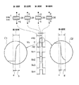
なお、駆動部12は、図2に示すような素子固定式構造のものではなく、例えば、図13に示すような自走式構造のものであっても上記の駆動回路14,14’により駆動することができる。図13(a)は自走式構造の駆動部12の分解斜視図であり、図13(b)はその駆動部12の正面図である。   Note that the drive unit 12 is not of the element fixed structure as shown in FIG. 2, but is driven by the drive circuits 14 and 14 ′, for example, of a self-running structure as shown in FIG. can do. FIG. 13A is an exploded perspective view of the drive unit 12 having a self-propelled structure, and FIG. 13B is a front view of the drive unit 12.

すなわち、この図13に示す駆動部12’は、位置固定される係合部材(ベース部材)40と移動部材42とから構成されている。係合部材40は、基板44と、基板44の略中央位置に所定の間隔をおいて対向配置され、板ばね等の弾性部材46,48により取り付けられた一対の狭持部材50,52と、基板44の左右両端部に取り付けられた一対のガイド部材54,56とを備えている。各ガイド部材54,56の外側面には、回転自在の複数のボール部材58,60が取り付けられている。   That is, the drive unit 12 ′ shown in FIG. 13 includes an engaging member (base member) 40 and a moving member 42 that are fixed in position. The engaging member 40 is disposed to face the substrate 44 at a substantially central position with a predetermined interval, and a pair of holding members 50 and 52 attached by elastic members 46 and 48 such as leaf springs, A pair of guide members 54 and 56 attached to both left and right ends of the substrate 44 are provided. A plurality of freely rotatable ball members 58 and 60 are attached to the outer surfaces of the guide members 54 and 56.

移動部材42は、駆動体63と、この駆動体63に一体に取り付けられた移動体65とから構成されている。駆動体63は、支持部材67、圧電素子69及び駆動部材71から構成されている。支持部材67は、圧電素子69及び駆動部材71を保持するものであり、直方体の軸方向両端部671,672及び略中央の仕切壁673を残して刳り貫くことにより形成された第1の収容空間674及び第2の収容空間675を有している。この第1の収容空間674には、圧電素子69がその伸縮方向を支持部材67の軸方向と一致させて収容されている。また、第2の収容空間675には、駆動部材71が軸方向に移動可能に収容されている。   The moving member 42 includes a driving body 63 and a moving body 65 attached to the driving body 63 integrally. The drive body 63 includes a support member 67, a piezoelectric element 69, and a drive member 71. The support member 67 holds the piezoelectric element 69 and the drive member 71, and is a first accommodation space formed by scoring the rectangular parallelepiped axial ends 671, 672 and a substantially central partition wall 673. 674 and a second accommodation space 675. In the first accommodation space 674, the piezoelectric element 69 is accommodated such that the expansion / contraction direction thereof coincides with the axial direction of the support member 67. Further, the drive member 71 is accommodated in the second accommodation space 675 so as to be movable in the axial direction.

圧電素子69は、図2に示す圧電素子26と同様に構成されたものであり、その伸縮方向(積層方向)である長手方向の一方端面が第1の収容空間674の一方端部671側端面に固着されている。駆動部材71は、支持部材67の左右両側に膨出する膨出部711が中央部に一体形成され、この膨出部711が第2の収容空間675に位置すると共に、仕切壁673に形成された貫通孔を介して第1の収容空間674内に突出した端部は圧電素子69の他方端面に固着され、支持部材67の他方端部672に形成された貫通孔を介して第2の収容空間675の外部に突出した端部は自由端とされている。   The piezoelectric element 69 is configured in the same manner as the piezoelectric element 26 shown in FIG. 2, and one end face in the longitudinal direction that is the expansion / contraction direction (stacking direction) is the end face on the one end portion 671 side of the first accommodation space 674. It is fixed to. In the drive member 71, a bulging portion 711 that bulges on both the left and right sides of the support member 67 is integrally formed at the center, and this bulging portion 711 is located in the second accommodation space 675 and is formed in the partition wall 673. The end projecting into the first accommodation space 674 through the through hole is fixed to the other end surface of the piezoelectric element 69, and the second accommodation through the through hole formed in the other end 672 of the support member 67. An end protruding outside the space 675 is a free end.

移動体65は、平板部651と、平板部651の左右両側に下方に伸びる側壁部652,653が形成されると共に、各側壁部652,653の内側に摺動部材654,655が形成されたもので、移動部材42における支持部材67の上面にねじ部材656により固定されている。   The moving body 65 has a flat plate portion 651 and side wall portions 652 and 653 extending downward on the left and right sides of the flat plate portion 651 and sliding members 654 and 655 formed inside the side wall portions 652 and 653. Therefore, the moving member 42 is fixed to the upper surface of the support member 67 by a screw member 656.

このように構成された移動部材42は、駆動部材71の膨出部711が係合部材40の一対の挟持部材50,52間に移動可能に挟持されることで係合部材40に組み付けられることになる。すなわち、係合部材40が図2の係合部材30に対応するものであり、この係合部材40が駆動部材71に対して所定の摩擦力で結合され、駆動部12’が構成されることになる。   The moving member 42 configured in this manner is assembled to the engaging member 40 by the bulging portion 711 of the driving member 71 being movably held between the pair of holding members 50 and 52 of the engaging member 40. become. That is, the engagement member 40 corresponds to the engagement member 30 of FIG. 2, and this engagement member 40 is coupled to the drive member 71 with a predetermined frictional force, so that the drive unit 12 ′ is configured. become.

この駆動部12’では、駆動回路14,14’から例えば図4(a)に示す波形を有する駆動電圧が印加されて圧電素子69が緩やかに伸長すると、駆動部材71が静止した状態で支持部材67が係合部材40の一方側に移動し、その後に圧電素子69が急激に縮小すると、支持部材67が静止した状態で駆動部材71が狭持部材50,52による摩擦力に打ち勝って係合部材40の一方側に移動する。この繰り返し動作により支持部材67が移動体65と共に、係合部材40の一方側に間欠的に移動することになる。   In the drive unit 12 ′, when a drive voltage having a waveform shown in FIG. 4A, for example, is applied from the drive circuits 14 and 14 ′ and the piezoelectric element 69 is gently expanded, the support member 71 is in a state where the drive member 71 is stationary. When 67 moves to one side of the engagement member 40 and then the piezoelectric element 69 rapidly shrinks, the drive member 71 overcomes the frictional force generated by the holding members 50 and 52 while the support member 67 is stationary. Move to one side of member 40. By this repetitive operation, the support member 67 moves intermittently to one side of the engagement member 40 together with the moving body 65.

また、駆動回路14,14’から例えば図4(b)に示す波形を有する駆動電圧が印加されて圧電素子69が急激に伸長すると、支持部材67が静止した状態で駆動部材71が狭持部材50,52による摩擦力に打ち勝って係合部材40の他方側に移動し、その後に圧電素子69が緩やかに縮小すると駆動部材71が静止した状態で支持部材67が係合部材40の他方側に移動する。この繰り返し動作により支持部材67が移動体65と共に、係合部材40の他方側に間欠的に移動することになる。   Further, when a driving voltage having a waveform shown in FIG. 4B, for example, is applied from the driving circuits 14 and 14 ′ and the piezoelectric element 69 is rapidly expanded, the driving member 71 is held in a state where the supporting member 67 is stationary. When the piezoelectric element 69 is gradually reduced after overcoming the frictional force of 50 and 52 and moved to the other side of the engaging member 40, the support member 67 is moved to the other side of the engaging member 40 with the drive member 71 stationary. Moving. The support member 67 moves intermittently to the other side of the engaging member 40 together with the moving body 65 by this repeated operation.

以上のように、本発明の実施形態に係る駆動装置10は、駆動回路14,14’が、圧電素子26にその一方側から駆動電圧を印加して充電する第1の駆動回路と、圧電素子26にその他方側から駆動電圧を印加して充電する第2の駆動回路と、各駆動回路により圧電素子26に充電された電荷を放電する放電回路とを備え、駆動制御手段は第1の駆動回路と第2の駆動回路とを交互に駆動させると共に、第1の駆動回路の駆動期間と第2の駆動回路の駆動期間との間に放電回路を駆動するようにしているので、圧電素子26を+Vpに充電するときも−Vpに充電するときにも充電に必要な電荷を供給するだけでよいことから駆動回路の複雑化等を招くことなく、消費電力を可及的に抑制して電池電源で有効に駆動することができるようになる。   As described above, in the driving apparatus 10 according to the embodiment of the present invention, the driving circuits 14 and 14 ′ apply the driving voltage to the piezoelectric element 26 from one side and charge the piezoelectric element 26, and the piezoelectric element. 26, a second driving circuit for charging by applying a driving voltage from the other side, and a discharging circuit for discharging the electric charge charged to the piezoelectric element 26 by each driving circuit, and the driving control means includes a first driving circuit. Since the circuit and the second drive circuit are driven alternately, and the discharge circuit is driven between the drive period of the first drive circuit and the drive period of the second drive circuit, the piezoelectric element 26 Since it is only necessary to supply the charge required for charging both when charging the battery to + Vp and without charging the battery, the power consumption is suppressed as much as possible without complicating the drive circuit. To be able to drive effectively with power supply That.

なお、本発明は、上記実施形態のものに限定されるものではなく、種々の変形態様を採用することができる。例えば、図3に示す駆動回路14の場合では、スイッチ素子Q2,Q4と大地との間に所定の抵抗値を有する抵抗素子を接続するようにしたり、図11に示す駆動回路14’の場合では、第5スイッチ回路155及び第6スイッチ回路156を除去する一方、スイッチ素子Q2,Q4と大地との間に所定の抵抗値を有する抵抗素子を接続するようにしたりすることができる。   In addition, this invention is not limited to the thing of the said embodiment, A various deformation | transformation aspect is employable. For example, in the case of the drive circuit 14 shown in FIG. 3, a resistance element having a predetermined resistance value is connected between the switch elements Q2 and Q4 and the ground, or in the case of the drive circuit 14 ′ shown in FIG. The fifth switch circuit 155 and the sixth switch circuit 156 can be removed, and a resistance element having a predetermined resistance value can be connected between the switch elements Q2 and Q4 and the ground.

10 圧電アクチュエータ(駆動装置)
12,12’ 駆動部
14,14’ 駆動回路
22 制御部(駆動制御手段)
24,67 支持部材
26,69 圧電素子(電気機械変換素子)
28,71 駆動部材
30,40 係合部材
141,151 第1スイッチ回路
142,152 第2スイッチ回路
143,153 第3スイッチ回路
144,154 第4スイッチ回路
155 第5スイッチ回路
156 第6スイッチ回路
Q1 スイッチ素子
Q2 スイッチ素子
Q3 スイッチ素子
Q4 スイッチ素子
Q5 スイッチ素子
Q6 スイッチ素子
R1,R2 抵抗素子
10 Piezoelectric actuator (drive device)
12, 12 'drive unit 14, 14' drive circuit 22 control unit (drive control means)
24, 67 Support member 26, 69 Piezoelectric element (electromechanical transducer)
28, 71 Drive member 30, 40 Engaging member 141, 151 First switch circuit 142, 152 Second switch circuit 143, 153 Third switch circuit 144, 154 Fourth switch circuit 155 Fifth switch circuit 156 Sixth switch circuit Q1 Switch element Q2 Switch element Q3 Switch element Q4 Switch element Q5 Switch element Q6 Switch element R1, R2 Resistance element

Claims (3)

駆動電圧が印加されることにより伸縮する電気機械変換素子と、該電気機械変換素子により駆動される駆動部材と、該駆動部材に所定の摩擦力で係合され、該駆動部材上を移動する係合部材と、前記電気機械変換素子を駆動する駆動回路と、該駆動回路の動作を制御する駆動制御手段とから構成され、前記電気機械変換素子を異なる速度で伸縮させることで前記電気機械変換素子と前記係合部材とを相対移動させる駆動装置において、
前記駆動回路は、前記電気機械変換素子の共振周波数に対して0.3倍より大きく1.5倍より小さい駆動周波数をもつ矩形波からなる駆動電圧を前記電気機械変換素子に印加することで、該駆動電圧が、前記駆動部材と係合部材との係合部分に、前記の伸縮時における速度差を生じさせることができる鋸歯状の変位振動を生じさせるものであることを特徴とする駆動装置。
An electromechanical transducer that expands and contracts when a drive voltage is applied, a drive member that is driven by the electromechanical transducer, and a mechanism that engages with the drive member with a predetermined frictional force and moves on the drive member. The electromechanical conversion element includes a combination member, a drive circuit that drives the electromechanical conversion element, and a drive control unit that controls the operation of the drive circuit. The electromechanical conversion element is expanded and contracted at different speeds. And a drive device for relatively moving the engaging member,
The drive circuit applies a drive voltage composed of a rectangular wave having a drive frequency larger than 0.3 times and smaller than 1.5 times to the resonance frequency of the electromechanical transducer, to the electromechanical transducer , The drive device is characterized in that the drive voltage causes a sawtooth-like displacement vibration capable of causing a speed difference at the time of expansion / contraction at an engagement portion between the drive member and the engagement member. .
前記駆動回路は、前記電気機械変換素子にその一方側から駆動電圧を印加して充電する第1の駆動回路と、前記電気機械変換素子にその他方側から駆動電圧を印加して充電する第2の駆動回路と、各駆動回路により電気機械変換素子に充電された電荷を放電する放電回路とを備え、前記駆動制御手段は、前記第1の駆動回路と第2の駆動回路とを交互に駆動させると共に、前記第1の駆動回路の駆動期間と第2の駆動回路の駆動期間との間に前記放電回路を駆動するようにしたことを特徴とする請求項1記載の駆動装置。   The drive circuit applies a drive voltage to the electromechanical conversion element from one side for charging, and a second drive circuit applies the drive voltage to the electromechanical conversion element from the other side for charging. Drive circuit and a discharge circuit for discharging the charge charged in the electromechanical conversion element by each drive circuit, and the drive control means drives the first drive circuit and the second drive circuit alternately. 2. The driving apparatus according to claim 1, wherein the discharge circuit is driven between a driving period of the first driving circuit and a driving period of the second driving circuit. 前記第1の駆動回路は、一方端が電源に接続され、他方端が前記電気機械変換素子の一方端に接続されてなる第1のスイッチ手段と、一方端が前記電気機械変換素子の他方端に接続され、他方端が接地されてなる第2のスイッチ手段とで構成されると共に、前記第2の駆動回路は、一方端が前記電源に接続され、他方端が前記電気機械変換素子の他方端に接続されてなる第3のスイッチ手段と、一方端が前記電気機械変換素子の一方端に接続され、他方端が接地されてなる第4のスイッチ手段とで構成され、前記放電回路は、前記第2のスイッチ手段と第4のスイッチ手段とで構成されていることを特徴とする請求項2記載の駆動装置。   The first drive circuit includes a first switch means having one end connected to a power source and the other end connected to one end of the electromechanical transducer, and one end connected to the other end of the electromechanical transducer. And the other end of the electromechanical conversion element is connected to the power source, and the other end of the electromechanical transducer is connected to the power source. A third switch means connected to one end, and a fourth switch means having one end connected to one end of the electromechanical transducer and the other end grounded. 3. A driving apparatus according to claim 2, wherein said driving device comprises said second switch means and fourth switch means.
JP2009298540A 2009-12-28 2009-12-28 Drive device Expired - Lifetime JP4666100B2 (en)

Priority Applications (1)

Application Number Priority Date Filing Date Title
JP2009298540A JP4666100B2 (en) 2009-12-28 2009-12-28 Drive device

Applications Claiming Priority (1)

Application Number Priority Date Filing Date Title
JP2009298540A JP4666100B2 (en) 2009-12-28 2009-12-28 Drive device

Related Parent Applications (1)

Application Number Title Priority Date Filing Date
JP2000012249A Division JP4470258B2 (en) 2000-01-20 2000-01-20 Drive device

Related Child Applications (1)

Application Number Title Priority Date Filing Date
JP2010085142A Division JP4706792B2 (en) 2010-04-01 2010-04-01 Drive device

Publications (2)

Publication Number Publication Date
JP2010104231A JP2010104231A (en) 2010-05-06
JP4666100B2 true JP4666100B2 (en) 2011-04-06

Family

ID=42294315

Family Applications (1)

Application Number Title Priority Date Filing Date
JP2009298540A Expired - Lifetime JP4666100B2 (en) 2009-12-28 2009-12-28 Drive device

Country Status (1)

Country Link
JP (1) JP4666100B2 (en)

Families Citing this family (1)

* Cited by examiner, † Cited by third party
Publication number Priority date Publication date Assignee Title
JP2019110382A (en) * 2017-12-15 2019-07-04 旭化成エレクトロニクス株式会社 Driving circuit

Family Cites Families (6)

* Cited by examiner, † Cited by third party
Publication number Priority date Publication date Assignee Title
JP3365248B2 (en) * 1996-04-15 2003-01-08 日立金属株式会社 Piezoelectric transformer and power conversion device using the same
JP3539117B2 (en) * 1997-03-03 2004-07-07 ミノルタ株式会社 Driving device using electromechanical transducer
JPH10290588A (en) * 1997-04-14 1998-10-27 Minolta Co Ltd Actuator using electromechanical transducer
JP3689783B2 (en) * 1997-11-21 2005-08-31 コニカミノルタフォトイメージング株式会社 Method for maintaining a constant feedback period, and drive control apparatus and optical apparatus controlled as such
JPH11341840A (en) * 1998-05-27 1999-12-10 Minolta Co Ltd Driver using electromechanical sensing element
JPH11356071A (en) * 1998-06-09 1999-12-24 Minolta Co Ltd Drive unit using electromechanical transducing element and driving circuit therefor

Also Published As

Publication number Publication date
JP2010104231A (en) 2010-05-06

Similar Documents

Publication Publication Date Title
JP4470258B2 (en) Drive device
JP5077403B2 (en) Drive device
US6512321B2 (en) Driving apparatus and method of using same
JP4804040B2 (en) Impact drive actuator
US7190104B2 (en) Device and method utilizing electromechanical conversion element
US7193351B2 (en) Driving device and driving method
JP4277384B2 (en) Piezoelectric actuator
KR20060106704A (en) Driving machanism
JP5104925B2 (en) Drive device
JP4706792B2 (en) Drive device
US6844658B2 (en) Drive apparatus
JP2005237144A (en) Piezoelectric actuator
JP4666100B2 (en) Drive device
US7608979B2 (en) Driving device and driving system
JP3722062B2 (en) Drive device
JP4492756B2 (en) Piezoelectric actuator
JP2005237145A (en) Drive circuit for piezoelectric element
JP3933460B2 (en) Drive device
JP3719197B2 (en) Drive device
JP3722050B2 (en) Drive device
KR100809754B1 (en) Drive unit
JP2004254412A (en) Drive circuit, driving method, and driver for electromechanical transducer
JP4492738B2 (en) Piezoelectric actuator
JP2002027767A (en) Driver
JP2000287466A5 (en)

Legal Events

Date Code Title Description
A131 Notification of reasons for refusal

Free format text: JAPANESE INTERMEDIATE CODE: A131

Effective date: 20100511

A521 Written amendment

Free format text: JAPANESE INTERMEDIATE CODE: A523

Effective date: 20100712

TRDD Decision of grant or rejection written
A01 Written decision to grant a patent or to grant a registration (utility model)

Free format text: JAPANESE INTERMEDIATE CODE: A01

Effective date: 20101214

A01 Written decision to grant a patent or to grant a registration (utility model)

Free format text: JAPANESE INTERMEDIATE CODE: A01

A61 First payment of annual fees (during grant procedure)

Free format text: JAPANESE INTERMEDIATE CODE: A61

Effective date: 20101227

FPAY Renewal fee payment (event date is renewal date of database)

Free format text: PAYMENT UNTIL: 20140121

Year of fee payment: 3

R150 Certificate of patent or registration of utility model

Ref document number: 4666100

Country of ref document: JP

Free format text: JAPANESE INTERMEDIATE CODE: R150

Free format text: JAPANESE INTERMEDIATE CODE: R150

S531 Written request for registration of change of domicile

Free format text: JAPANESE INTERMEDIATE CODE: R313531

S533 Written request for registration of change of name

Free format text: JAPANESE INTERMEDIATE CODE: R313533

R350 Written notification of registration of transfer

Free format text: JAPANESE INTERMEDIATE CODE: R350

EXPY Cancellation because of completion of term