JP4650748B2 - Magnetic deflector and ion implantation system for ion implantation system - Google Patents
Magnetic deflector and ion implantation system for ion implantation system Download PDFInfo
- Publication number
- JP4650748B2 JP4650748B2 JP2006533770A JP2006533770A JP4650748B2 JP 4650748 B2 JP4650748 B2 JP 4650748B2 JP 2006533770 A JP2006533770 A JP 2006533770A JP 2006533770 A JP2006533770 A JP 2006533770A JP 4650748 B2 JP4650748 B2 JP 4650748B2
- Authority
- JP
- Japan
- Prior art keywords
- coil
- ion beam
- pair
- ion
- magnetic
- Prior art date
- Legal status (The legal status is an assumption and is not a legal conclusion. Google has not performed a legal analysis and makes no representation as to the accuracy of the status listed.)
- Expired - Lifetime
Links
- 238000005468 ion implantation Methods 0.000 title claims description 19
- 238000010884 ion-beam technique Methods 0.000 claims description 108
- 150000002500 ions Chemical class 0.000 claims description 46
- 239000002245 particle Substances 0.000 claims description 31
- 230000007935 neutral effect Effects 0.000 claims description 20
- 238000011109 contamination Methods 0.000 claims description 16
- 230000005686 electrostatic field Effects 0.000 claims description 7
- 239000004020 conductor Substances 0.000 claims description 3
- 238000000034 method Methods 0.000 description 14
- 239000007789 gas Substances 0.000 description 13
- 239000004065 semiconductor Substances 0.000 description 11
- 238000010586 diagram Methods 0.000 description 9
- 239000002019 doping agent Substances 0.000 description 8
- 230000000694 effects Effects 0.000 description 8
- 238000006386 neutralization reaction Methods 0.000 description 7
- 238000004458 analytical method Methods 0.000 description 5
- 230000005684 electric field Effects 0.000 description 5
- 238000002347 injection Methods 0.000 description 5
- 239000007924 injection Substances 0.000 description 5
- 238000002513 implantation Methods 0.000 description 4
- 239000000463 material Substances 0.000 description 4
- 230000007246 mechanism Effects 0.000 description 4
- 239000000356 contaminant Substances 0.000 description 3
- 230000006870 function Effects 0.000 description 3
- 230000008569 process Effects 0.000 description 3
- 241000894007 species Species 0.000 description 3
- 238000009792 diffusion process Methods 0.000 description 2
- 238000012545 processing Methods 0.000 description 2
- 238000010926 purge Methods 0.000 description 2
- 241000287463 Phalacrocorax Species 0.000 description 1
- 230000001133 acceleration Effects 0.000 description 1
- 230000002411 adverse Effects 0.000 description 1
- 230000000712 assembly Effects 0.000 description 1
- 238000000429 assembly Methods 0.000 description 1
- 230000004888 barrier function Effects 0.000 description 1
- 230000008901 benefit Effects 0.000 description 1
- 230000015572 biosynthetic process Effects 0.000 description 1
- 230000008859 change Effects 0.000 description 1
- 230000001143 conditioned effect Effects 0.000 description 1
- 238000012937 correction Methods 0.000 description 1
- 230000003247 decreasing effect Effects 0.000 description 1
- 238000009826 distribution Methods 0.000 description 1
- 238000000605 extraction Methods 0.000 description 1
- 239000007943 implant Substances 0.000 description 1
- 239000012535 impurity Substances 0.000 description 1
- 238000001802 infusion Methods 0.000 description 1
- 230000003993 interaction Effects 0.000 description 1
- -1 ion ions Chemical class 0.000 description 1
- 238000002955 isolation Methods 0.000 description 1
- 238000004519 manufacturing process Methods 0.000 description 1
- 238000004949 mass spectrometry Methods 0.000 description 1
- 238000012986 modification Methods 0.000 description 1
- 230000004048 modification Effects 0.000 description 1
- 230000003472 neutralizing effect Effects 0.000 description 1
- 230000003287 optical effect Effects 0.000 description 1
- 229910052573 porcelain Inorganic materials 0.000 description 1
- 230000001681 protective effect Effects 0.000 description 1
- 230000009467 reduction Effects 0.000 description 1
- 230000004044 response Effects 0.000 description 1
- 239000000758 substrate Substances 0.000 description 1
- 238000012546 transfer Methods 0.000 description 1
- 238000011144 upstream manufacturing Methods 0.000 description 1
- 229910052724 xenon Inorganic materials 0.000 description 1
- FHNFHKCVQCLJFQ-UHFFFAOYSA-N xenon atom Chemical compound [Xe] FHNFHKCVQCLJFQ-UHFFFAOYSA-N 0.000 description 1
Images


Classifications
-
- H—ELECTRICITY
- H01—ELECTRIC ELEMENTS
- H01J—ELECTRIC DISCHARGE TUBES OR DISCHARGE LAMPS
- H01J37/00—Discharge tubes with provision for introducing objects or material to be exposed to the discharge, e.g. for the purpose of examination or processing thereof
- H01J37/30—Electron-beam or ion-beam tubes for localised treatment of objects
- H01J37/317—Electron-beam or ion-beam tubes for localised treatment of objects for changing properties of the objects or for applying thin layers thereon, e.g. for ion implantation
- H01J37/3171—Electron-beam or ion-beam tubes for localised treatment of objects for changing properties of the objects or for applying thin layers thereon, e.g. for ion implantation for ion implantation
-
- H—ELECTRICITY
- H01—ELECTRIC ELEMENTS
- H01J—ELECTRIC DISCHARGE TUBES OR DISCHARGE LAMPS
- H01J37/00—Discharge tubes with provision for introducing objects or material to be exposed to the discharge, e.g. for the purpose of examination or processing thereof
- H01J37/30—Electron-beam or ion-beam tubes for localised treatment of objects
-
- H—ELECTRICITY
- H01—ELECTRIC ELEMENTS
- H01J—ELECTRIC DISCHARGE TUBES OR DISCHARGE LAMPS
- H01J37/00—Discharge tubes with provision for introducing objects or material to be exposed to the discharge, e.g. for the purpose of examination or processing thereof
- H01J37/02—Details
- H01J37/04—Arrangements of electrodes and associated parts for generating or controlling the discharge, e.g. electron-optical arrangement or ion-optical arrangement
- H01J37/05—Electron or ion-optical arrangements for separating electrons or ions according to their energy or mass
-
- H—ELECTRICITY
- H01—ELECTRIC ELEMENTS
- H01J—ELECTRIC DISCHARGE TUBES OR DISCHARGE LAMPS
- H01J37/00—Discharge tubes with provision for introducing objects or material to be exposed to the discharge, e.g. for the purpose of examination or processing thereof
- H01J37/02—Details
- H01J37/04—Arrangements of electrodes and associated parts for generating or controlling the discharge, e.g. electron-optical arrangement or ion-optical arrangement
- H01J37/147—Arrangements for directing or deflecting the discharge along a desired path
-
- H—ELECTRICITY
- H01—ELECTRIC ELEMENTS
- H01J—ELECTRIC DISCHARGE TUBES OR DISCHARGE LAMPS
- H01J2237/00—Discharge tubes exposing object to beam, e.g. for analysis treatment, etching, imaging
- H01J2237/05—Arrangements for energy or mass analysis
- H01J2237/057—Energy or mass filtering
Landscapes
- Chemical & Material Sciences (AREA)
- Analytical Chemistry (AREA)
- Physical Vapour Deposition (AREA)
- Plasma Technology (AREA)
- Electron Sources, Ion Sources (AREA)
- Drying Of Semiconductors (AREA)
Description
本発明は、一般的には、イオン注入システムに関し、より詳しくは、イオン注入システムにおいてイオンビームを低エネルギーに減速するために用いられる偏向システムに関する。 The present invention relates generally to ion implantation systems and, more particularly, to a deflection system used to decelerate an ion beam to low energy in an ion implantation system.
イオン注入システムは、集積回路の製造において、半導体に不純物をドープするために使用される。イオン注入システムでは、イオン源で所望のドーパント元素がイオン化され、イオン化されたドーパント元素は、イオンビームとしてイオン源から引き出される。イオンビームは、通常、質量分析によって所望の質量対電荷比を有するイオンが選択され、半導体ウエハ等の加工物の表面に導かれて、そのドーパント元素がウエハに注入される。ビーム中のイオンは、例えばウエハにトランジスタ素子を作製する場合には、加工物の表面を貫通して所望の導電率の領域を形成する。典型的なイオン注入装置には、イオンビームを発生するイオン源と、磁界を使用してイオンビームを質量分析するための質量分析磁石を含むビームラインアセンブリーと、そのイオンビームが注入される半導体ウエハまたは加工物を収容するターゲットチャンバーとが含まれる。 Ion implantation systems are used to dope semiconductors with impurities in the manufacture of integrated circuits. In an ion implantation system, a desired dopant element is ionized in an ion source, and the ionized dopant element is extracted from the ion source as an ion beam. As the ion beam, ions having a desired mass-to-charge ratio are usually selected by mass spectrometry, guided to the surface of a workpiece such as a semiconductor wafer, and the dopant element is implanted into the wafer. The ions in the beam penetrate the surface of the workpiece to form a region with a desired conductivity, for example, when a transistor element is fabricated on a wafer. A typical ion implanter includes an ion source that generates an ion beam, a beam line assembly that includes a mass analysis magnet for mass analyzing the ion beam using a magnetic field, and a semiconductor into which the ion beam is implanted. And a target chamber containing a wafer or workpiece.
所定の用途に応じた所望の注入を達成するために、注入されるイオンの線量およびエネルギーを変更することができる。イオン線量によって、所定の半導体材料に注入されるイオンの濃度が制御される。典型的には、高線量注入には高電流注入装置が使用され、比較的低線量の用途には中電流注入装置が使用される。イオンエネルギーは、半導体素子の接合深度を制御するために使用され、半導体または他の基板に注入されるイオンの深さがイオンビーム中のイオンのエネルギーレベルによって定まる。半導体素子の微細化が進むにつれて、高ビーム電流を低エネルギーで供給することが要求されている。高ビーム電流によって必要な線量レベルが達成され、低エネルギーによって浅い注入が可能になる。 In order to achieve the desired implantation for a given application, the dose and energy of the implanted ions can be varied. The concentration of ions implanted into a predetermined semiconductor material is controlled by the ion dose. Typically, high current implanters are used for high dose implants and medium current implanters are used for relatively low dose applications. Ion energy is used to control the junction depth of a semiconductor device, and the depth of ions implanted into a semiconductor or other substrate is determined by the energy level of the ions in the ion beam. As miniaturization of semiconductor elements progresses, it is required to supply a high beam current with low energy. High beam current achieves the required dose level and low energy allows shallow implantation.
中電流注入システムは、通常、枚葉式システムであると共に大ティルト角での注入を可能にするものである。そのようなシステムは、通常、中エネルギーから高エネルギーの範囲(例えば、10〜250keV)での低線量処理または中線量処理に適している。低エネルギーでは、ビームライン中の様々な光学要素を通じて、ビーム輸送効率が低いために、ビーム電流供給能力が大幅に低下する。ビーム輸送効率を改善するために一般に使用される技術は、高エネルギーでビームを伝播させ、その後、加工物から短距離の位置で所望のエネルギーにビームを減速することである。通常、減速率を高くする程、ビーム輸送効率におけるゲインが向上する。 Medium current injection systems are typically single wafer systems and allow injection at large tilt angles. Such systems are usually suitable for low dose or medium dose processing in the medium to high energy range (eg, 10-250 keV). At low energy, the beam current supply capability is greatly reduced due to low beam transport efficiency through various optical elements in the beam line. A commonly used technique to improve beam transport efficiency is to propagate the beam with high energy and then decelerate the beam to the desired energy at a short distance from the workpiece. In general, the higher the deceleration rate, the better the gain in beam transport efficiency.
しかしながら、上述したような減速システムでは、加工物に、望ましくないエネルギーコンタミネーションが生じる場合がある。エネルギーコンタミネーションは、減速前にビーム内に発生した中性粒子がターゲットに到達可能となる状態である。中性粒子は減速されないため、イオンビームの他の部分よりも大幅に高いエネルギーで加工物に到達することができ、そのような状態をしばしばエネルギーコンタミネーションと呼ぶものである。 However, in the deceleration system as described above, undesirable energy contamination may occur in the workpiece. Energy contamination is a state in which neutral particles generated in the beam before deceleration can reach the target. Since neutral particles are not decelerated, they can reach the workpiece with much higher energy than other parts of the ion beam, and such conditions are often referred to as energy contamination.
本発明の1つまたは複数の態様の基本的理解のために、本発明の簡単な要約を以下に示す。この要約は、本発明の完全な概要ではなく、また、本発明の重要な要素を同定するものでも、本発明の範囲を画定するものでもない。この要約の主要な目的は、後述する詳細な説明の導入として、本発明の概念の幾つかを簡略化された形式で提示することである。 For a basic understanding of one or more aspects of the invention, a brief summary of the invention is provided below. This summary is not an extensive overview of the invention and it does not identify key elements of the invention or delineate the scope of the invention. The primary purpose of this summary is to present some concepts of the invention in a simplified form as a prelude to the more detailed description that is presented later.
本発明は、イオン注入システムにおける磁気偏向器に関する。この磁気偏向器は、ビームの伝播方向にほぼ直交するほぼ均一な磁界を発生する。この磁界によって、イオンビーム(例えば、ペンシル形ビームまたはリボン形ビーム)中の移動するイオンに力が作用し、それによって、イオンビームはビーム軸から偏向する。この偏向によって、エネルギーコンタミネーションとして作用する中性粒子がビームから除去される。 The present invention relates to a magnetic deflector in an ion implantation system. The magnetic deflector, generates a substantially uniform magnetic field that is substantially Cartesian the propagation direction of the beam. This magnetic field exerts a force on the moving ions in the ion beam (eg, pencil or ribbon beam), thereby deflecting the ion beam from the beam axis. This deflection removes neutral particles acting as energy contamination from the beam.
本発明の一態様において、磁気偏向器は、イオンビームの上方および下方にそれぞれ配置された一対のコイルを含む。これらのコイルは、それらを通じて流れる電流に応じて、コイル間に、ビームの伝播方向にほぼ直交する磁界を発生させる。これらのコイルは、イオンビームがリボン形ビーム、または、リボン形ビームに見えるスキャンビームの場合、好ましくは、イオンビームの全幅に沿って横方向に延在し、それによって、ビームの全幅に沿って均一な磁界を発生するものである。加えて、コイル間の領域にプラズマを導入し、特に、ビームエネルギーが低い場合に、空間電荷の中性化を促進するものであってもよい。プラズマは、コイル間の磁力線に沿って拡散し、ビームの幅に沿ってほぼ均一に空間電荷を中性化するものである。 In one aspect of the present invention, the magnetic deflector includes a pair of coils respectively disposed above and below the ion beam. These coils generate a magnetic field approximately perpendicular to the beam propagation direction between the coils in response to the current flowing through them. These coils preferably extend laterally along the full width of the ion beam, if the ion beam is a ribbon beam or a scan beam that appears to be a ribbon beam, and thereby along the full width of the beam. A uniform magnetic field is generated. In addition, plasma may be introduced into the region between the coils, and particularly when the beam energy is low, neutralization of space charge may be promoted. The plasma diffuses along the lines of magnetic force between the coils and neutralizes the space charge almost uniformly along the width of the beam.
本発明の一態様では、イオン注入システムにおいて、磁気方式と静電方式のハイブリッド偏向システムが使用される。このハイブリッド偏向システムは、磁気偏向モジュールおよび静電偏向モジュールと、1つまたは複数の入力制御信号に基づいて、磁気偏向モジュールと静電偏向モジュールの1つを選択的に動作させるように作動可能なコントローラーとを含んでいる。例えば、コントローラーは、1つまたは複数の入力制御信号が、質量エネルギー積が予め定められた閾値よりも小さいことを示す場合に、磁気偏向モジュールを動作させ、質量エネルギー積が閾値よりも大きい場合に、静電偏向モジュールを動作させるように作動可能なものである。上記の方法において、このハイブリッドシステムは、低いビームエネルギーで磁気偏向を使用するものであり、この場合、プラズマを使用して、低エネルギーで問題となる空間電荷効果の影響を軽減してもよい。同様に、空間電荷効果が明白でないときに磁気硬度の限界が現れた場合には、このハイブリッドシステムは、比較的高いビームエネルギーで静電偏向を使用してもよい。 In one aspect of the invention, a magnetic and electrostatic hybrid deflection system is used in an ion implantation system. The hybrid deflection system is operable to selectively operate one of the magnetic deflection module and the electrostatic deflection module based on the magnetic deflection module and the electrostatic deflection module and one or more input control signals. Includes a controller. For example, the controller operates the magnetic deflection module when the one or more input control signals indicate that the mass energy product is less than a predetermined threshold, and the mass energy product is greater than the threshold. And operable to operate the electrostatic deflection module. In the above method, the hybrid system uses magnetic deflection with low beam energy, and in this case, plasma may be used to mitigate the effects of space charge effects that are problematic at low energy. Similarly, if a magnetic hardness limit appears when space charge effects are not evident, the hybrid system may use electrostatic deflection with relatively high beam energy.
本発明に従って、このハイブリッド偏向器は、ペンシル形ビーム、リボン形ビーム、または、リボン形と同様の性質を有するペンシル形スキャンビームに対して適用することができる。 In accordance with the present invention, the hybrid deflector can be applied to a pencil-shaped beam, a ribbon-shaped beam, or a pencil-shaped scan beam having properties similar to a ribbon-shaped beam.
上記目的および関連する目的を達成するために、以下の説明および添付図面には、本発明の特定の例示的な態様および実施形態が詳細に記載されているが、これらは、本発明の原理を使用可能な様々な態様のごく一部を示すものである。本発明の他の態様、利点、および新規な特徴は、以下の本発明の詳細な説明を図面と共に考慮することによって、明らかになるであろう。 To the accomplishment of the above and related ends, the following description and the annexed drawings set forth in detail certain illustrative aspects and embodiments of the invention. Only a few of the various aspects that can be used are shown. Other aspects, advantages and novel features of the invention will become apparent from the following detailed description of the invention when considered in conjunction with the drawings.
以下、添付図面を参照して本発明を説明する。全体を通じて、同様の構成要素には同様の符号を付して参照する。添付図面および以下の説明は、例示のためのものであり、本発明を限定するものではない。したがって、例示されたシステムおよび方法の変形例、並びに、本明細書に例示されたシステムおよび方法とは異なる他の実施形態は、本発明および添付請求項の範囲に含まれるものである。 Hereinafter, the present invention will be described with reference to the accompanying drawings. Throughout, like components are referred to with like reference numerals. The accompanying drawings and the following description are for purposes of illustration and are not intended to limit the invention. Accordingly, variations of the illustrated systems and methods, as well as other embodiments that differ from the systems and methods illustrated herein, are within the scope of the present invention and the appended claims.
本発明は、低エネルギーのイオンビームを得るための減速システムと共に使用される偏向システムに関する。この偏向システムは、中性粒子が加工物に到達することを回避するために、イオンビームを受容して、そのイオンビームを入射ビームライン軸から加工物に向けて偏向する。以下に説明するように、本発明は、イオンビームをビームライン軸から偏向するように動作可能な磁気偏向器を含む。この磁気偏向器は、さらに、静電偏向器と共に使用してハイブリッド偏向システムを形成するものであってもよい。この場合、磁気偏向モジュールは、比較的低いイオンビームエネルギーにおける偏向に使用され、静電偏向モジュールは、比較的高いビームエネルギーにおける偏向に使用される。本発明は、ペンシル形ビームの注入システムおよびリボン形ビームの注入システムの両方に適用することができる。 The present invention relates to a deflection system for use with a deceleration system to obtain a low energy ion beam. The deflection system receives an ion beam and deflects the ion beam from the incident beam line axis toward the workpiece to avoid neutral particles reaching the workpiece. As described below, the present invention includes a magnetic deflector operable to deflect an ion beam from the beam line axis. This magnetic deflector may also be used with an electrostatic deflector to form a hybrid deflection system. In this case, the magnetic deflection module is used for deflection at a relatively low ion beam energy, and the electrostatic deflection module is used for deflection at a relatively high beam energy. The present invention can be applied to both pencil beam injection systems and ribbon beam injection systems.
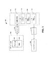
まず、図1を参照すると、本発明の1つまたは複数の態様を実施するために好適なイオン注入システム100が、ブロック図で示されている。システム100は、ビーム経路に沿ってイオンビーム104を生成するためのイオンビーム源102を含む。以下に詳述するように、このイオンビームは、ペンシル形ビームからなるものであってもよく、または、リボン形ビームからなるものであってもよい。イオンビーム源102は、例えば、電源108を備えたプラズマ源106を含んでいる。プラズマ源106は、例えば、プラズマ閉じ込めチャンバーを含み、このプラズマ閉じ込めチャンバーからイオンビームが引き出される。
Referring first to FIG. 1, a block diagram of an
イオンビーム源102の下流には、そこからイオンビーム104を受容するビームラインアセンブリー110が備えられている。ビームラインアセンブリー110は、質量分析器112、スキャナー114(ペンシル形システムの場合)、減速システム116、および偏向器118を含んでいてもよい。質量分析器112は、例えば磁石(図示省略)のような磁界を発生する構成要素を含み、質量(例えば、電荷対質量比)に応じた様々な軌道でイオンビーム104からイオンを偏向するために、ビーム経路に交差する磁界を発生する。
Downstream of the
スキャナー114は、ペンシル形ビームを制御された方法で加工物全域に方向付ける(走査する)ために、ビームライン軸の方向を調整し、それによって、リボン形ビームの効果を生じさせるものである。スキャナーは、静電方式または磁気方式のいずれであってもよく、また、任意のそのような走査機構または他のタイプのシステムを本発明と共に使用することもできる。ペンシル形ビームを走査してリボン状ビームを生成する代わりに、リボン形ビームを直接生成するイオンビーム源を使用することもできる。本発明と共に使用できるリボンビーム源の一例は、2002年5月1日に出願され、本発明の譲受人に譲受された米国特許出願第10/136,047号に開示されており、その内容は参考として本明細書に含まれる。
The
ビームライン110は、さらに、減速モジュール116を含む。この減速モジュールは、イオンビームに関連するエネルギーを変更させるように制御可能かつ選択的に動作可能なものである。例えば、中程度のエネルギーでは、ビームエネルギーの実質的な変更は要しないため、このモジュールは、イオンビームが実質的な変更を受けることなく通過できるようにするものである。一方、低エネルギーの用途(例えば、半導体における浅い接合の形成)では、ビームエネルギーの減速を要する場合がある。このような状況において、減速システム116は、イオンビームを減速することによって、所望のエネルギーレベルまでビームのエネルギーを低減することができる。
The
ビームラインは、本発明に従う偏向システム118を含んでいる。偏向システム118は、磁気偏向器を含み、減速システム116を通過した後に、イオンビームをビームライン軸から偏向するように動作する。例えば、入射ビームが減速されていたとしても、イオンビームに伴って移動する中性粒子はどれも減速されていない。そして、そのような中性粒子は、イオンビームを偏向しなければ、エネルギーコンタミネーションとして加工物に到達してしまう。偏向システム118の磁気偏向器は、このような状況下で、イオンビームを、ビームライン軸から加工物に向けて偏向するものである。このとき、中性粒子は、磁気偏向器によって偏向されず、以前のビームライン軸に沿って移動するため、加工物には到達しない。
The beamline includes a
中性の汚染粒子は、偏向システムの上流領域において、イオンおよび背景(残留)粒子間の衝突によって生成される可能性がある。このような衝突によって、一部のイオンが背景粒子または他の粒子と電荷を交換する現象が生じ、それによって、中性粒子(汚染粒子)となる。これらの中性粒子は、ウエハの、イオンが注入されるべき領域に注入されると、意図されたドープのレベルを希釈して、ドープ処理に悪影響を及ぼす可能性がある。さらに重要なことは、これらの粒子は、電気的に中性であるため、減速器、より詳細には、電極によって発生する静電界を、その影響(例えば、減速、集束、屈折、または、速さおよび/または方向に関する他の変更)を受けることなく通過することである。したがって、これらの粒子は、加速器を通過して調整されたイオンビーム中の、曲げられ、集束され、加速および/または減速されたイオンとは、その(影響を受けていない)エネルギーレベルが異なっている可能性が高いため、ウエハに望ましくない深さで注入されるおそれがある。この中性粒子による汚染(コンタミネーション)は、半導体デバイスの所望の性能を大幅に劣化させる可能性がある。 Neutral contaminant particles can be generated by collisions between ions and background (residual) particles in the upstream region of the deflection system. Such a collision causes a phenomenon in which some ions exchange charges with background particles or other particles, thereby becoming neutral particles (contamination particles). These neutral particles, when implanted in the region of the wafer where ions are to be implanted, can dilute the intended dope level and adversely affect the doping process. More importantly, since these particles are electrically neutral, the effect of the electrostatic field generated by the decelerator, and more particularly the electrodes, is reduced (eg, decelerated, focused, refracted, or accelerated). (And other changes with respect to height and / or direction). Thus, these particles differ in their (unaffected) energy level from bent, focused, accelerated and / or decelerated ions in an ion beam conditioned through an accelerator. Can be implanted at an undesirable depth into the wafer. This contamination by neutral particles can significantly degrade the desired performance of the semiconductor device.
本発明は、その1つまたは複数の態様において、中性粒子による汚染に取り組むものであり、少なくとも、イオンビームを屈折することによって、イオンをビーム中の中性汚染粒子から逸らすものである。除染されたイオンビームは、例えば、汚染粒子の経路から約5〜25度の角度だけ偏向させることができる。汚染粒子は、電気的に中性であり、電極によって影響を受けないため、汚染粒子の経路はイオンビームの元の経路である。このイオンビームは、加工物に導かれ、加工物の選択領域に注入するために、その領域に衝突する。汚染粒子が加工物またはウエハに衝突することを避けるために、例えば、ある種の障壁を中性粒子の流れの前に配置することもできる。 The present invention, in one or more aspects thereof, addresses contamination by neutral particles and at least diverts ions from neutral contamination particles in the beam by refracting the ion beam. The decontaminated ion beam can be deflected, for example, by an angle of about 5-25 degrees from the path of the contaminating particles. Since the contaminant particles are electrically neutral and are not affected by the electrodes, the contaminant particle path is the original path of the ion beam. This ion beam is directed to the workpiece and impinges on that region for injection into a selected region of the workpiece. In order to avoid contamination particles impinging on the workpiece or wafer, for example, certain barriers can be placed in front of the neutral particle flow.
本発明はまた、その1つまたは複数の態様において、イオンビームのブローアップの問題にも取り組むものである。イオンビームのブローアップは、同種の荷電粒子が反発する特性の結果として生じる。イオンビームを形成する正に帯電したイオンは、いわゆる「空間電荷力」のために、互いに反発する。空間電荷効果は、イオンビームエネルギーの3/2乗に反比例するため、イオンビーム中のイオンが減速されると増大し、イオンビームが分散(ブローアップ)する傾向が増大する。空間電荷力のため、イオンビームの横方向の広がりは、次式に比例する。 The present invention also addresses, in one or more aspects thereof, the problem of ion beam blow-up. Ion beam blow-up occurs as a result of the repulsive nature of similar charged particles. The positively charged ions that form the ion beam repel each other due to so-called “space charge forces”. Since the space charge effect is inversely proportional to the 3/2 power of the ion beam energy, when the ions in the ion beam are decelerated, the tendency of the ion beam to disperse (blow up) increases. Due to space charge forces, the lateral extent of the ion beam is proportional to:

ここで、mはイオンの質量、qはイオンの電荷、Iはビーム電流、Uはビームエネルギー、zはイオンビームの伝播距離である。ただし、イオンビームは、均一であると仮定されている。このように、ビームエネルギーが減少すると、ビームのブローアップの可能性が増大することが分かる。したがって、イオンビームのエネルギーが低い場合、特に、ビームが減速されていると共に、ビーム電流が大きいかまたはビーム中のイオン濃度が大きい場合には、すべてのイオンをウエハに到達させることが困難になる。 Here, m is the mass of the ion, q is the charge of the ion, I is the beam current, U is the beam energy, and z is the propagation distance of the ion beam. However, the ion beam is assumed to be uniform. Thus, it can be seen that decreasing the beam energy increases the likelihood of beam blow-up. Therefore, when the energy of the ion beam is low, particularly when the beam is decelerated and the beam current is large or the ion concentration in the beam is large, it becomes difficult to make all the ions reach the wafer. .
本発明の磁気偏向器は、低エネルギーにおける静電偏向機構に比べて有利なものである。低エネルギーでは、空間電荷力に関連する問題は悪化し、望ましくないビームのブローアップの傾向が生じる。磁界の存在下で生じる偏向と共に、そこでプラズマを使用することによって、空間電荷の中性化を促進することができる。磁界は、一般に、磁力線を横切るプラズマの拡散に対して抵抗を与えるが、磁力線に沿ったプラズマの拡散には、ほとんど抵抗を示さない。以下に詳述するように、磁界の方向は、ビームの伝播方向(または輸送方向)にほぼ直交する方向であるため、プラズマは、リボン形ビーム、または、加工物付近でリボン状に見えるペンシル形スキャンビームのいずれの場合でも、ビームの全幅を横断して容易に拡散することができる。これによって、イオンビームに関連する空間電荷の均一な中性化が促進される。 The magnetic deflector of the present invention is advantageous compared to an electrostatic deflection mechanism at low energy. At low energies, the problems associated with space charge forces are exacerbated and an undesirable beam blow-up tendency occurs. The neutralization of the space charge can be promoted by using the plasma there along with the deflection that occurs in the presence of the magnetic field. The magnetic field generally provides resistance to plasma diffusion across the field lines, but exhibits little resistance to plasma diffusion along the field lines. As detailed below, the direction of the magnetic field is approximately perpendicular to the direction of propagation (or transport) of the beam, so the plasma is either a ribbon beam or a pencil shape that looks like a ribbon near the workpiece. In either case, the scan beam can be easily diffused across the full width of the beam. This promotes uniform neutralization of the space charge associated with the ion beam.
再び図1を参照すると、システム100は、質量分析されて実質的に除染されたイオンビーム119を、ビームラインアセンブリー110から受容するエンドステーション120も備えている。エンドステーション120は、イオンビーム119を使用した注入処理のために、例えば半導体ウエハ(図示省略)のような1つまたは複数の加工物を、ビーム経路(ただし、偏向器118により元のビームライン軸からは逸れた経路)に沿って支持するものである。
Referring again to FIG. 1, the
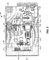
図2は、中電流かつ低エネルギーのペンシル形ビームまたはリボン形ビームを、本発明の1つまた複数の態様に従って形成するために好適な、例示的なイオン注入システム200をより詳細に示した図である。システム200は、例えば、モジュール型のガスボックス202、補助ガスボックス204、およびガスボックスのパージのリモートコントロールパネル206を含む。ガスボックス202、204は、他の物質と共に、ドーパント物質の1種または複数種のガスを含んでおり、システム200内の長寿命化イオン源208中に、1種または複数種のガスを選択的に供給できるようにするものである。1種または複数種のガスは、イオン源208でイオン化され、システムに選択的に搬入されるウエハまたは加工物に注入するために好適なイオンが発生する。ガスボックスのリモートコントロールパネル206は、1種または複数種のガスまたは他の物質を、必要に応じてシステム200から排気(パージ)する、
FIG. 2 illustrates in greater detail an exemplary
システム200には、ドーパントガスを電気的に励起してエネルギーを付与することによってガスからイオンを生成するために、他の構成要素と共に、高圧端子電力分配器210および高圧絶縁トランス212が含まれている。また、イオン源208からイオンを引き出して、そのイオンをビームライン216に加速するために、イオンビーム引出アセンブリー214が含まれている。ビームラインアセンブリー216は、質量分析磁石218を含むものである。質量分析磁石218は、不適当な電荷対質量比を有するイオンを除外する。特に、質量分析磁石218は、曲面状の側壁を有するビームガイドを含んでおり、不適当な質量対電荷比を有するイオンは、ビームガイドを通じて伝播すると、1つまたは複数の磁界によってその側壁に衝突する。
システム200には、スキャンビームの角度制御を補助するための構成要素220を含めることもできる。この構成要素は、他の要素と共に、走査角度補正レンズを含んでいてもよい。加速/減速カラム222は、イオンビーム中のイオンの速度および/または集束を、容易に制御および調整できるようにするものである。さらに、システム200には、偏向システム224が含まれており、この偏向システム224は、上述したように、汚染粒子を除去し、エネルギーコンタミネーションの要因となる粒子のウエハまたは加工物への衝突を軽減するものである。
The
ウエハまたは加工物226は、イオンの選択的注入のために、ステーションチャンバー228内にロードされる。機械的スキャンドライブ230は、チャンバー228内のウエハを操作して、ビームに対して選択的に衝突できるようにするものである。ウエハまたは加工物226は、ウエハ操作システム232によって、エンドステーションチャンバー228内に搬入される。ウエハ操作システムは、例えば、1つまたは複数の機械的アームまたはロボットアーム234を含んでいてもよい。オペレーターは、オペレーターコンソール236によって、システム200の1つまたは複数の構成要素を選択的に制御して、注入処理を調整するものである。最後に、システム200全体に電力を供給するために、電力分配ボックス238が備えられている。
A wafer or workpiece 226 is loaded into the
図3Aを参照すると、図1および図2に示すシステム118、224のような、本発明の一態様に従った例示的な偏向システム300が示されている。偏向システム300は、コントローラー304に結合された磁気偏向器302を含み、磁気偏向器302は、プラズマ源306に作動的に関連するものである。磁気偏向器302は、1つまたは複数の入力制御信号308に基づいてコントローラー304によって動作し、イオンビーム313の伝播方向312にほぼ直交する(または、横断する)磁界を領域310に発生する。この例において、イオンビームは、ペンシル形ビーム、ペンシル形スキャンビーム(したがって、走査のためにリボン状に見える)、またはリボン形ビーム、および本発明において考えられる全ての代替的なビーム形状である。より詳細には、磁界310は、イオンビームを、ビームライン軸314から加工物318に向かう方向316に偏向するように作用するものである。
Referring to FIG. 3A, an
磁気偏向器302は、ビームを横断するほぼ均一な磁界を生成し、リボン形ビームまたはリボン形と同様のビームの場合には、ビーム313の全幅(図示省略)にわたってほぼ均一な磁界を生成する。この結果、方向316に沿ったビーム313の偏向は、ビームの全幅にわたってほぼ均一に生じるため、リボン形ビームの均一性を保持するために有利なものである。加えて、プラズマ源306は、領域310にプラズマを供給し、低いビームエネルギーで重要な、ビームに関連する空間電荷の中性化を促進する。低いビームエネルギーでの偏向に磁界を使用することは、磁界がプラズマによって消失または押し流されないため、有利なものである。むしろ、プラズマは、通常、磁力線に沿って領域310を通じて拡散することができる。
The
磁界は、ローレンツ力の式:F=q(v×B)に従って、ビーム313中のイオンを偏向するように作用する。ここで、磁界ベクトルBによって示される方向を有する磁界下で、速度ベクトルvによって示される方向に移動する電荷に作用する力は、力ベクトルFによって示される方向を有する。より詳細には、図3Bに示すように、ビーム320中のイオンが正に帯電したイオンであり、速度VでZ方向に伝播しており、かつ、磁界がその伝播方向に直交するX方向を向いている場合、イオンに作用する力は、Yの負方向である。この例では、図示されるように、紙面の下方向である。
The magnetic field acts to deflect ions in the
プラズマ源306は、磁界領域310と作動的に関連している。一例では、このプラズマは、この領域中に存在する任意の残留ガスと、ビーム中のイオンとの相互作用によって生じるビームプラズマである。あるいは、プラズマ源は、例えばキセノンのような高い電離効率を有するガス源であってもよい。さらに別の例として、プラズマ源306は、プラズマフラッド(plasma flood)、または、プラズマを生成して磁界領域に入射させる他のタイプの装置であってもよい。
磁界領域中の磁界がイオンビーム中のイオンを偏向するように作用するものであるため、その磁界は、イオンビームにわたって可能な限り均一であることが望ましく、特に、リボン形ビームまたはリボン形と同様のビームを使用する場合には、ビームの全幅にわたって均一であることが望ましい。リボン形ビームが300mm半導体ウエハにわたって走査される1つの例示的な用途では、リボン形ビームは300mmを超える幅を有しており、したがって、磁界は、リボン形ビームの縁部の歪みを最小限に抑えるために、そのリボンの幅に相当する、リボンの幅よりも実質的には大きな距離にわたって均一であるものである。 Since the magnetic field in the magnetic field region acts to deflect ions in the ion beam, it is desirable that the magnetic field be as uniform as possible across the ion beam, particularly as in a ribbon beam or ribbon shape. When using two or more beams, it is desirable to be uniform over the entire width of the beam. In one exemplary application where the ribbon beam is scanned across a 300 mm semiconductor wafer, the ribbon beam has a width greater than 300 mm, and therefore the magnetic field minimizes the distortion of the ribbon beam edge. In order to suppress, it is uniform over a distance substantially larger than the width of the ribbon, which corresponds to the width of the ribbon.
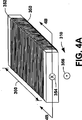
本発明の1つの例示的な態様に従って、磁気偏向器302の磁界は、一対のコイルを使用して発生させるものであり、それらの一方が、図4Aに、符号350を付して示されている。コイル350は、一例として、ヨーク352に巻回された導体を含んでいる。コイル350を通じて電流が流れると、そのループを通じて、閉じた経路を形成する磁力線を伴う磁界が発生する。図4Bに示すように、コイル350を通じて流れる電流(I)が、時計回り(電子は反時計回り)である場合、図4Aに示すように、右手の法則に従って、ヨーク中の354で紙面に入り、リボン形ビームが伝播する磁界領域310の356で紙面から出る磁界が発生する。コイル350がヨーク352に沿って延在している距離または横幅360を、リボン形ビームの幅よりも大きくすることにより、ビームの全幅に沿ってほぼ均一な磁界が存在することになる。あるいは、例えば、永久磁石または電磁石のような、双極子磁界を発生する他のメカニズムを使用することもできる。
In accordance with one exemplary aspect of the present invention, the magnetic field of
図5Aに、一対のコイル350を使用した磁気偏向器を有するシステム400を示す。ここで、第1のコイル350aは、ビーム313の上方に配置され、第1のコイル350bは、ビーム313の下方に配置されている。第1および第2のコイル350は、互いに他方のコイルと関連して、領域310に、ビームの伝播方向にほぼ直交する磁界402を形成する。さらに、この例では、第1および第2のコイル350は、入力端部が開口部サイズ404を有し、入力端部の下流側に配置された出力端部は、入力端部よりも大きな開口部サイズ406を有するように構成されている。出力端部の開口部が大きいことによって、加工物318に向けて偏向された経路に沿って、ビームを物理的に崩壊させることなく、ビームを偏向することができる。
FIG. 5A shows a
一対のコイル350a,350bを有することは、リボン形ビームまたはリボン形と同様のビームの、幅方向および高さ方向の両方に対して均一な磁界402を形成するために役立つ。コイル350のそれぞれは、同方向に流れる電流を有しており、それぞれのコイルによって結果として生じる磁界は、互いに打ち消し合うのではなく、互いに加算されるように重ね合わされる。これらのコイルの一方または両方の電流を変動することによって、所望の制御に応じて、ビームの偏向量を調整するか、あるいは、様々に異なるドーパント化学種またはビームエネルギーに対して所定の偏向を達成するために、磁界領域310中の磁界402の強さを調整することができる。
Having a pair of
図5Bは、本発明の例示的な一態様に従う磁気偏向器を示す透視図である。図5Bにおいて、一対のコイル350a、350bは、単一のヨーク352を介して結合された配置をとるものである。加えて、中性粒子は偏向されないため、依然として以前のビームライン軸に沿って伝播するそのような中性粒子を捕獲または収集するために、偏向器の後方に保護プレート380が配置されている。さらに、コイル間に配置されたヨークの側方部分にマルチカスプ磁石を使用することもでき、これは、リボン形ビームまたはリボン形と同様のビームの縁部において、電子を閉じ込めるために役立つものである。
FIG. 5B is a perspective view illustrating a magnetic deflector according to an exemplary embodiment of the present invention. In FIG. 5B, the pair of
本発明の別の態様に従って、図6Aには、磁気/静電式ハイブリッド偏向システム500が示されている。ハイブリッド偏向システム500は、磁気偏向モジュールと静電偏向モジュールを、それぞれ含んでいる。磁気偏向モジュールは、図6Aに、ビーム313の上方および下方にそれぞれ配置された一対のコイル350として示されている。この例では、静電偏向モジュールは、一対の電極504、または、ビームの上方および下方にそれぞれ配置された横方向に延在する導電板として示されている。磁気偏向モジュールおよび静電偏向モジュールの両方は、コントローラー304に作動的に結合されており、コントローラーは、1つまたは複数の入力信号308に基づいて、上記モジュールの1つを選択的に動作させることができる。
In accordance with another aspect of the present invention, FIG. 6A illustrates a magnetic / electrostatic
本発明の1つの例示的な態様では、コントローラ304は、ビームの質量エネルギー積に基づいて、上記モジュールの1つを選択的に動作させるものである。例えば、図6Bに示すように、コントローラー304は、質量エネルギー積が予め定められた閾値よりも小さい場合、磁気偏向モジュールを動作させ、また、場合によっては(例えば、偏向領域510内でビームが磁界520によって偏向された場合)プラズマ源306を動作させる。同様に、コントローラー304が、1つおよび複数の入力制御信号308に基づいて、質量エネルギー積が閾値よりも大きいと判別した場合には、コントローラーは、静電偏向モジュールを選択的に動作させ、静電界506を使用して、電界/磁界領域510内でのイオンビーム偏向を達成する。
In one exemplary aspect of the present invention, the
本発明に係るハイブリッド偏向器500は、空間電荷効果が重要な低エネルギーでは、磁気偏向器を使用するものである。磁気偏向器を使用することによって、電界/磁界領域510でプラズマを使用することが可能となるため、空間電荷の中性化が促進される。電界/磁界領域510中のプラズマにとって、磁力線を横断する方向には抵抗が存在するため、プラズマが磁力線を横断しようとすることはない。しかし、プラズマ抵抗は、磁力線に沿った方向では大幅に低減する。その結果、電界/磁界領域510中のプラズマは、磁力線に沿って、ビームの幅方向(リボン形ビーム、または、リボン形と同様のビームの場合)に拡散する傾向を有する。それによって、電界/磁界領域510中でプラズマの十分な均一化が可能となり、空間電荷の中性化における均一性が促進される。
The
比較的高いビームエネルギーでは、高エネルギーにおける空間電荷効果の低減のためプラズマが存在しないことに関わらず、静電偏向モジュールを通じて大きなビーム電流が輸送される。したがって、質量エネルギー積が予め定められた閾値(例えば、4000keV−amu)よりも大きい場合、コントローラーは、静電偏向モジュールを選択的に動作させる。このとき、電極504には、電界/磁界領域510に静電界506を形成するように、バイアス電圧が印加される。静電界中のイオンには、式:F=qEに従って力が作用する。ここで、電荷には、静電界の方向に力が作用する。好ましくは、電極504は、ビーム上に作用する静電界が、リボン形ビームまたはリボン形と同様のビームの全幅に沿ってほぼ均一となるようなビーム構成において、少なくともビームの全幅に沿って横方向に延在するものであり、それによって、ビームの縁部に沿った歪みが低減される。磁気偏向は、比較的高いエネルギーにおいて磁気硬度による限界が存在するため、このような比較的高いエネルギーでは、静電偏向が有利である。
At relatively high beam energies, large beam currents are transported through the electrostatic deflection module regardless of the absence of a plasma due to the reduction of space charge effects at high energies. Therefore, when the mass energy product is larger than a predetermined threshold (for example, 4000 keV-amu), the controller selectively operates the electrostatic deflection module. At this time, a bias voltage is applied to the
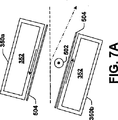
本発明の参考例において、図7Aおよび図7Bにそれぞれ示すように、一対のコイル350a、350bは、様々な方向を備えていてもよい。図7Aに示すように、両コイルは、互いに平行に配置されると共に、ビームライン軸に平行に配置されていてもよい。あるいは、図7Bに示すように、コイル350a、350bは、互いに平行に配置されると共に、偏向後の軸に平行に配置されていてもよい。これらの配置の場合、システムへの入口の開口部404は、出口の開口部406とほぼ同一のサイズである。このようなコイルの配置構成および他のコイルの配置構成を使用することもできる。
In the reference example of the present invention, as shown in FIGS. 7A and 7B, the pair of
本発明の一態様に従う磁気偏向器を備えた偏向システム使用して、イオンビームを加工物に向けて偏向させるための方法600を図8に示す。方法600は、一連の動作または事象として図示され、また、以下に記載されているが、本発明は、そのような動作または事象の順番に限定されるものではない。例えば、本発明の1つまたは複数の態様に従って、本明細書に図示および/または記載されたものから逸脱して、いくつかの動作は、異なる順序で発生するものであっても、または、他の動作または事象と同時に発生するものであっても、あるいは、それらの両方であってもよい。加えて、本発明に係る方法を実施するために、必ずしも例示されたすべてのステップが必要なわけではない。さらに、本発明に係る方法は、本明細書に図示および記載された構造物の形成および/または処理に関連して実施できるだけでなく、例示されていない他の構造物に関連して実施することもできる
Use deflection system including a slave cormorants magnetic deflector to an aspect of the present invention, Figure 8 shows the
この方法600は、ステップ602から開始する。ステップ602において、例えばコントローラーが、1つまたは複数の入力制御信号を受信する。制御信号は、例えば、使用されるドーパント化学種、およびビーム(例えば、リボン形ビーム)の所望のエネルギーを反映するものであってもよく、これらの制御信号は、偏向システムに導入する前に、分析後減速が必要か否か、あるいは、どの程度の分析後減速が必要かを判別するために使用される。ドーパント化学種および最終エネルギーレベルに関する情報と共に、ステップ604において、質量エネルギー積(MEP:mass-energy product)が判別され、ステップ606において、そのMEPが予め定められた閾値よりも大きいか否かが判別される。この判別に基づいて、2つの異なるモジュールの1つを動作させる。ステップ606において、MEPが閾値よりも小さかった場合(はい)、ステップ608において、上記記載において詳述したような磁気偏向モジュールを動作させ、また、ステップ610において、プラズマを導入するかまたは生成して、空間電荷の中性化を促進するものである。
The
一方、ステップ606において、MEPが予め定められた閾値よりも大きかった場合(いいえ)、ステップ612において、静電偏向モジュールを動作させるものである。質量エネルギー積またはビームエネルギーのような判断基準に基づいて、異なるタイプの偏向器を使用することによって、偏向メカニズムを低エネルギーに対して適切なものに調整することができる。その結果、空間電荷の中性化により、低エネルギーにおいて、比較的高いビーム電流を効率的に使用することができる。
On the other hand, when the MEP is larger than the predetermined threshold value in Step 606 (No), the electrostatic deflection module is operated in
以上、本発明を特定の態様および実施形態に関連させて図示および説明してきたが、本明細書および添付された図面の理解に基づいて、当業者が同等な変更および修正に想至し得ることは理解されるであろう。特に、上述した構成要素(アセンブリー、装置、回路、システム等)によって実行される種々の機能に関して、そのような構成要素を説明するために使用された用語(「手段」に対する参照を含む)は、特に明示されない限り、ここに示された本発明の例示的な実施形態において特定の機能を実行する上述した構成要素のその機能を実行する(すなわち、機能的に同等である)任意の構成要素に、たとえ開示された構成に構造的に同等でなくても、相当するものである。この点に関して、本発明は、本発明の様々な方法のステップを実施するためのコンピュータで実行可能な指令を有する、コンピュータで読取り可能な媒体を含むものである。加えて、本発明の特定の特徴がいくつかの態様のうちの1つのみに関連して開示された場合であっても、所定のまたは特定の用途のために望ましくかつ有利であるように、そのような特徴を他の態様の1つまたはそれ以上の特徴と組み合わせることもできる。本発明において、用語「リボン形と同様のビーム」は、リボン形ビーム、および、ペンシル形スキャンビームを含むものである。さらに、用語「含む(include)」、「含んでいる(including)」、「有する(have)」、「有している(having)」、及びそれらの変化形が発明の詳細な説明または請求項で使用されている範囲に関して、これらの用語は、用語「含んでいる(comprising)」と同様な意味で包含的なものであることが意図されている。また、本明細書で使用されている用語「例示的な(exemplary)」は、最良の実施形態ではなく、単に一例を意味するものとして使用されている。 While the invention has been illustrated and described in connection with specific aspects and embodiments, those skilled in the art will perceive equivalent changes and modifications based on an understanding of this specification and the accompanying drawings. Will be understood. In particular, with respect to the various functions performed by the components described above (assemblies, devices, circuits, systems, etc.), the terms used to describe such components (including references to “means”) are: Unless stated otherwise, any component that performs that function (ie, is functionally equivalent) of the above-described components that perform a particular function in the exemplary embodiments of the invention shown herein. Even if it is not structurally equivalent to the disclosed configuration, it is equivalent. In this regard, the present invention includes a computer-readable medium having computer-executable instructions for performing the various method steps of the present invention. In addition, even if certain features of the present invention are disclosed in connection with only one of several aspects, it may be desirable and advantageous for a given or specific application, Such features can also be combined with one or more features of other aspects. In the present invention, the term “beam similar to a ribbon shape” includes a ribbon shape beam and a pencil shape scan beam. Further, the terms “include”, “including”, “have”, “having”, and variations thereof are detailed descriptions or claims of the invention. With respect to the ranges used in, these terms are intended to be inclusive in a manner similar to the term “comprising”. Also, as used herein, the term “exemplary” is not intended to be the best embodiment, but merely as an example.
Claims (12)
さらに、前記第1のコイルと前記イオンビームの間に配置された第1の電極と、前記第2のコイルと前記イオンビームの間に配置された第2の電極とからなる一対の電極を含み、該一対の電極は、該一対の電極の間に、該一対の電極の間を通過する前記イオンビームを偏向するための静電界を発生することを特徴とする磁気偏向器。A magnetic deflector for an ion beam comprising a ribbon beam or a pencil scan beam, comprising a pair of coils comprising a first coil and a second coil, the first coil being above the ion beam Wherein the second coil is disposed below the ion beam, both the first coil and the second coil extend along the width of the ion beam, and The first coil and the second coil are used to deflect the ion beam away from the beam line axis by one predetermined deflection amount to remove neutral particles acting as energy contamination from the ion beam. By passing a direct current through the coil in the same direction, the ion beam is moved between the first coil and the second coil. A substantially uniform magnetic field is induced along the entire width in a direction substantially perpendicular to the propagation direction of the ion beam, and the first coil and the second coil are directed to the magnetic deflector of the ion beam. And an output end of the ion beam from the magnetic deflector, the output end being located downstream of the input end, and an opening of the output end is much larger than the opening of the input end, wherein each of the first coil and the second coil, and a yoke extending in the width direction along the entire width of the ion beam, the yoke A conductor wound and extending in the width direction along the entire width of the ion beam,
And a pair of electrodes including a first electrode disposed between the first coil and the ion beam, and a second electrode disposed between the second coil and the ion beam. The pair of electrodes generates an electrostatic field between the pair of electrodes for deflecting the ion beam passing between the pair of electrodes .
前記イオンビームを受容して、不要の質量対電荷比を有するイオンを除去するように作動可能な質量分析器と、
前記リボン形イオンビームまたは前記ペンシル形ビームが走査されてなるペンシル形スキャンビームからなるイオンビームをビームライン軸に沿って受容し、磁界を使用して前記ビームライン軸から前記イオンビームを偏向するように作動可能な磁気偏向器と、
を含んでおり、
前記磁気偏向器は、第1のコイルおよび第2のコイルを含み、前記第1のコイルは前記イオンビームの上方に配置され、前記第2のコイルは前記イオンビームの下方に配置されており、前記第1のコイルおよび前記第2のコイルの両方は、前記イオンビームの幅に沿って延在し、さらに、前記イオンビームを1つの所定の偏向量をもって前記ビームライン軸から離れるように偏向させて前記イオンビームからエネルギーコンタミネーションとして作用する中性粒子を除去するために、前記第1のコイルおよび前記第2のコイルを通じて同方向に直流電流を流すことによって、前記第1のコイルと前記第2のコイルの間に、前記イオンビームのほぼ全幅に沿って、前記イオンビームの伝播方向にほぼ直交する方向に、ほぼ均一な磁界を誘導するとともに、前記第1のコイルおよび前記第2のコイルは、前記イオンビームの前記磁気偏向器への入力端部と前記イオンビームの前記磁気偏向器からの出力端部を形成するように配置されており、前記出力端部は前記入力端部の下流に位置し、前記出力端部の開口部は、前記入力端部の開口部よりも大きく、前記第1のコイルおよび前記第2のコイルのそれぞれは、前記イオンビームの全幅に沿ってその幅方向に延在するヨークと、前記ヨークに巻回され、前記イオンビームの全幅に沿ってその幅方向に延在する導体とを含んでおり、さらに、前記第1のコイルと前記イオンビームの間に配置された第1の電極と、前記第2のコイルと前記イオンビームの間に配置された第2の電極とからなる一対の電極を含み、該一対の電極は、該一対の電極の間に、該一対の電極の間を通過する前記イオンビームを偏向するための静電界を発生することを特徴とするイオン注入システム。 An ion source operable to generate a ribbon ion beam or a pencil ion beam;
A mass analyzer operable to receive the ion beam and remove ions having an unwanted mass-to-charge ratio;
An ion beam comprising a ribbon-type ion beam or a pencil-type scan beam scanned with the pencil-type beam is received along a beam line axis, and a magnetic field is used to deflect the ion beam from the beam line axis. A magnetic deflector operable to
Contains
The magnetic deflector includes a first coil and a second coil, the first coil is disposed above the ion beam, and the second coil is disposed below the ion beam, Both the first coil and the second coil extend along the width of the ion beam, and further deflect the ion beam away from the beam line axis by one predetermined deflection amount. In order to remove neutral particles that act as energy contamination from the ion beam, a direct current is passed in the same direction through the first coil and the second coil, whereby the first coil and the first coil Between the two coils, a substantially uniform magnetic field is induced along substantially the entire width of the ion beam in a direction substantially perpendicular to the propagation direction of the ion beam. Both the first coil and the second coil are arranged to form an input end of the ion beam to the magnetic deflector and an output end of the ion beam from the magnetic deflector. The output end is located downstream of the input end, and the opening of the output end is larger than the opening of the input end, and each of the first coil and the second coil Includes a yoke extending in the width direction along the entire width of the ion beam, and a conductor wound around the yoke and extending in the width direction along the entire width of the ion beam. A pair of electrodes consisting of a first electrode disposed between the first coil and the ion beam, and a second electrode disposed between the second coil and the ion beam, The pair of electrodes is the pair of electrodes. Ion implantation system, wherein the during, generates an electrostatic field for deflecting the ion beam passing between the pair of electrodes.
Applications Claiming Priority (2)
| Application Number | Priority Date | Filing Date | Title |
|---|---|---|---|
| US10/461,702 US6881966B2 (en) | 2003-05-15 | 2003-06-13 | Hybrid magnetic/electrostatic deflector for ion implantation systems |
| PCT/US2004/018788 WO2004114354A2 (en) | 2003-06-13 | 2004-06-14 | A hybrid magnetic/electrostatic deflector for ion implantation systems |
Related Child Applications (1)
| Application Number | Title | Priority Date | Filing Date |
|---|---|---|---|
| JP2009046436A Division JP4645965B2 (en) | 2003-06-13 | 2009-02-27 | Magnetic / electrostatic hybrid deflector for ion implantation system and ion beam deflection method |
Publications (3)
| Publication Number | Publication Date |
|---|---|
| JP2007517358A JP2007517358A (en) | 2007-06-28 |
| JP2007517358A5 JP2007517358A5 (en) | 2007-11-29 |
| JP4650748B2 true JP4650748B2 (en) | 2011-03-16 |
Family
ID=33538973
Family Applications (2)
| Application Number | Title | Priority Date | Filing Date |
|---|---|---|---|
| JP2006533770A Expired - Lifetime JP4650748B2 (en) | 2003-06-13 | 2004-06-14 | Magnetic deflector and ion implantation system for ion implantation system |
| JP2009046436A Expired - Lifetime JP4645965B2 (en) | 2003-06-13 | 2009-02-27 | Magnetic / electrostatic hybrid deflector for ion implantation system and ion beam deflection method |
Family Applications After (1)
| Application Number | Title | Priority Date | Filing Date |
|---|---|---|---|
| JP2009046436A Expired - Lifetime JP4645965B2 (en) | 2003-06-13 | 2009-02-27 | Magnetic / electrostatic hybrid deflector for ion implantation system and ion beam deflection method |
Country Status (7)
| Country | Link |
|---|---|
| US (1) | US6881966B2 (en) |
| EP (1) | EP1634316B1 (en) |
| JP (2) | JP4650748B2 (en) |
| KR (1) | KR101157676B1 (en) |
| CN (2) | CN101777481B (en) |
| TW (1) | TWI314337B (en) |
| WO (1) | WO2004114354A2 (en) |
Families Citing this family (37)
| Publication number | Priority date | Publication date | Assignee | Title |
|---|---|---|---|---|
| JP4964413B2 (en) * | 2004-11-30 | 2012-06-27 | 株式会社Sen | Ion beam / charged particle beam irradiation system |
| JP4901094B2 (en) * | 2004-11-30 | 2012-03-21 | 株式会社Sen | Beam irradiation device |
| JP5042451B2 (en) * | 2004-11-30 | 2012-10-03 | 株式会社Sen | Beam space charge neutralization apparatus and ion implantation apparatus having the same |
| US7598505B2 (en) * | 2005-03-08 | 2009-10-06 | Axcelis Technologies, Inc. | Multichannel ion gun |
| US7361913B2 (en) | 2005-04-02 | 2008-04-22 | Varian Semiconductor Equipment Associates, Inc. | Methods and apparatus for glitch recovery in stationary-beam ion implantation process using fast ion beam control |
| US7674687B2 (en) * | 2005-07-27 | 2010-03-09 | Silicon Genesis Corporation | Method and structure for fabricating multiple tiled regions onto a plate using a controlled cleaving process |
| US7675047B2 (en) * | 2005-11-15 | 2010-03-09 | Varian Semiconductor Equipment Associates, Inc. | Technique for shaping a ribbon-shaped ion beam |
| US7800082B2 (en) * | 2006-02-15 | 2010-09-21 | Varian Semiconductor Equipment Associates, Inc. | Electromagnet with active field containment |
| US7863157B2 (en) * | 2006-03-17 | 2011-01-04 | Silicon Genesis Corporation | Method and structure for fabricating solar cells using a layer transfer process |
| WO2007118121A2 (en) | 2006-04-05 | 2007-10-18 | Silicon Genesis Corporation | Method and structure for fabricating solar cells using a layer transfer process |
| TWI435378B (en) * | 2006-04-26 | 2014-04-21 | Axcelis Tech Inc | Dose uniformity correction technique |
| JP4828305B2 (en) * | 2006-05-30 | 2011-11-30 | 株式会社Sen | Electrostatic beam deflection scanning apparatus and beam deflection scanning method |
| US8153513B2 (en) * | 2006-07-25 | 2012-04-10 | Silicon Genesis Corporation | Method and system for continuous large-area scanning implantation process |
| US7227160B1 (en) | 2006-09-13 | 2007-06-05 | Axcelis Technologies, Inc. | Systems and methods for beam angle adjustment in ion implanters |
| US7507978B2 (en) * | 2006-09-29 | 2009-03-24 | Axcelis Technologies, Inc. | Beam line architecture for ion implanter |
| US7750320B2 (en) * | 2006-12-22 | 2010-07-06 | Axcelis Technologies, Inc. | System and method for two-dimensional beam scan across a workpiece of an ion implanter |
| US7586111B2 (en) * | 2007-07-31 | 2009-09-08 | Axcelis Technologies, Inc. | Ion implanter having combined hybrid and double mechanical scan architecture |
| US20090206275A1 (en) * | 2007-10-03 | 2009-08-20 | Silcon Genesis Corporation | Accelerator particle beam apparatus and method for low contaminate processing |
| US20100065761A1 (en) * | 2008-09-17 | 2010-03-18 | Axcelis Technologies, Inc. | Adjustable deflection optics for ion implantation |
| US9443698B2 (en) * | 2008-10-06 | 2016-09-13 | Axcelis Technologies, Inc. | Hybrid scanning for ion implantation |
| US8466431B2 (en) * | 2009-02-12 | 2013-06-18 | Varian Semiconductor Equipment Associates, Inc. | Techniques for improving extracted ion beam quality using high-transparency electrodes |
| US8232532B2 (en) * | 2009-06-23 | 2012-07-31 | Hitachi Global Storage Technologies Netherlands B.V. | Off-axis ion milling device for manufacture of magnetic recording media and method for using the same |
| CN101838797B (en) * | 2009-12-18 | 2012-07-04 | 上海凯世通半导体有限公司 | Ion implantation method |
| JP5500500B2 (en) * | 2010-03-11 | 2014-05-21 | 日新イオン機器株式会社 | Ion implanter with beam deflector having asymmetric Einzel lens |
| US8847159B2 (en) | 2011-03-28 | 2014-09-30 | Tokyo Electron Limited | Ion energy analyzer |
| CN102751155B (en) * | 2011-04-22 | 2015-02-11 | 上海凯世通半导体有限公司 | Beam transmission system and beam transmission method |
| JP5800286B2 (en) * | 2012-03-09 | 2015-10-28 | 日新イオン機器株式会社 | Ion implanter |
| US20150228445A1 (en) * | 2014-02-13 | 2015-08-13 | Varian Semiconductor Equipment Associates, Inc. | Method and apparatus for three dimensional ion implantation |
| US9455116B2 (en) | 2014-04-30 | 2016-09-27 | Axcells Technologies, Inc. | Angular scanning using angular energy filter |
| CN105895486A (en) * | 2014-12-18 | 2016-08-24 | 北京中科信电子装备有限公司 | Charged particle beam deflection magnetic field structure and ion implantation machine using structure |
| CN106653533B (en) * | 2015-11-04 | 2018-08-14 | 北京中科信电子装备有限公司 | A kind of ion implantation apparatus of charged particle line magnetic field focusing structure and the application structure |
| JP6854628B2 (en) * | 2016-11-10 | 2021-04-07 | 東京エレクトロン株式会社 | Plasma spraying device and thermal spraying control method |
| US10580616B2 (en) | 2017-10-09 | 2020-03-03 | Axcelis Technologies, Inc. | System and method for in-situ beamline film stabilization or removal in the AEF region |
| WO2020055894A1 (en) * | 2018-09-10 | 2020-03-19 | Exogenesis Corporation | Method and apparatus to eliminate contaminants from an accelerated neutral atom beam to protect a beam target |
| CN109473344B (en) * | 2018-11-13 | 2021-08-03 | 上海华力微电子有限公司 | Ion implantation method and equipment |
| EP4000355A4 (en) * | 2019-07-19 | 2023-06-28 | Phoenix, LLC | Gas jet deflection in pressurized systems |
| CN112799120B (en) * | 2019-11-13 | 2024-03-22 | 中国科学院国家空间科学中心 | Dual-channel electrostatic analyzer for synchronous measurement of ions and electrons |
Family Cites Families (42)
| Publication number | Priority date | Publication date | Assignee | Title |
|---|---|---|---|---|
| FR2412939A1 (en) * | 1977-12-23 | 1979-07-20 | Anvar | HIGH CURRENT ION IMPLANTER |
| US4737644A (en) * | 1985-10-30 | 1988-04-12 | International Business Machines Corporation | Conductive coated semiconductor electrostatic deflection plates |
| JPH0731996B2 (en) * | 1985-11-14 | 1995-04-10 | 日新電機株式会社 | Ion implanter |
| JP2706471B2 (en) * | 1987-09-30 | 1998-01-28 | 日本真空技術株式会社 | Parallel sweep device for electrostatic sweep type ion implanter |
| DE68922929T2 (en) * | 1988-03-23 | 1996-02-22 | Fujitsu Ltd., Kawasaki, Kanagawa | Photocathode image projection apparatus for patterning on a semiconductor device. |
| JPH02260356A (en) * | 1989-03-31 | 1990-10-23 | Ulvac Corp | Parallel scanning system in ion implantation apparatus |
| GB9005204D0 (en) * | 1990-03-08 | 1990-05-02 | Superion Ltd | Apparatus and methods relating to scanning ion beams |
| US5132544A (en) * | 1990-08-29 | 1992-07-21 | Nissin Electric Company Ltd. | System for irradiating a surface with atomic and molecular ions using two dimensional magnetic scanning |
| US5311028A (en) * | 1990-08-29 | 1994-05-10 | Nissin Electric Co., Ltd. | System and method for producing oscillating magnetic fields in working gaps useful for irradiating a surface with atomic and molecular ions |
| JPH04171648A (en) * | 1990-11-05 | 1992-06-18 | Nec Corp | Ion implanter |
| JPH04171647A (en) * | 1990-11-05 | 1992-06-18 | Nec Corp | Ion implanter |
| US5206516A (en) * | 1991-04-29 | 1993-04-27 | International Business Machines Corporation | Low energy, steered ion beam deposition system having high current at low pressure |
| JPH0547339A (en) * | 1991-08-21 | 1993-02-26 | Nec Corp | Ion implanter |
| JP3448352B2 (en) * | 1994-07-07 | 2003-09-22 | 株式会社日立製作所 | Method for manufacturing semiconductor device |
| JP3358336B2 (en) * | 1994-10-14 | 2002-12-16 | 日新電機株式会社 | Method for detecting abnormal implantation conditions in ion implantation system |
| US5468955A (en) * | 1994-12-20 | 1995-11-21 | International Business Machines Corporation | Neutral beam apparatus for in-situ production of reactants and kinetic energy transfer |
| JPH08212965A (en) * | 1995-01-31 | 1996-08-20 | Ulvac Japan Ltd | Ion implanting device |
| GB2344214B (en) | 1995-11-08 | 2000-08-09 | Applied Materials Inc | An ion implanter with improved beam definition |
| JPH09213250A (en) * | 1996-01-30 | 1997-08-15 | Jeol Ltd | Deflection device for charged particle beam |
| US5693939A (en) * | 1996-07-03 | 1997-12-02 | Purser; Kenneth H. | MeV neutral beam ion implanter |
| JP3635818B2 (en) * | 1996-10-03 | 2005-04-06 | 日新電機株式会社 | Ion implanter |
| JPH10199460A (en) * | 1997-01-09 | 1998-07-31 | Jeol Ltd | Focusing ion beam device |
| JP3371753B2 (en) * | 1997-04-25 | 2003-01-27 | 日新電機株式会社 | Ion implanter |
| US5780863A (en) | 1997-04-29 | 1998-07-14 | Eaton Corporation | Accelerator-decelerator electrostatic lens for variably focusing and mass resolving an ion beam in an ion implanter |
| JP3449198B2 (en) * | 1997-10-22 | 2003-09-22 | 日新電機株式会社 | Ion implanter |
| JPH11176372A (en) * | 1997-12-11 | 1999-07-02 | Ulvac Corp | Ion irradiation device |
| JPH11283552A (en) * | 1998-03-31 | 1999-10-15 | Tadamoto Tamai | Device and method for ion implantation, ion-beam source and variable slit mechanism |
| GB9813327D0 (en) * | 1998-06-19 | 1998-08-19 | Superion Ltd | Apparatus and method relating to charged particles |
| JP2002525820A (en) | 1998-09-24 | 2002-08-13 | コーニンクレッカ フィリップス エレクトロニクス エヌ ヴィ | Ion implanter arranged to select neutral ions from ion beam |
| US6441382B1 (en) | 1999-05-21 | 2002-08-27 | Axcelis Technologies, Inc. | Deceleration electrode configuration for ultra-low energy ion implanter |
| US6635880B1 (en) * | 1999-10-05 | 2003-10-21 | Varian Semiconductor Equipment Associates, Inc. | High transmission, low energy beamline architecture for ion implanter |
| US6313428B1 (en) * | 1999-10-12 | 2001-11-06 | Advanced Ion Beam Technology, Inc. | Apparatus and method for reducing space charge of ion beams and wafer charging |
| US6521895B1 (en) | 1999-10-22 | 2003-02-18 | Varian Semiconductor Equipment Associates, Inc. | Wide dynamic range ion beam scanners |
| JP2001126656A (en) * | 1999-10-25 | 2001-05-11 | Nissin Electric Co Ltd | Ion implantation device |
| US6489622B1 (en) | 2000-03-01 | 2002-12-03 | Advanced Ion Beam Technology, Inc. | Apparatus for decelerating ion beams with minimal energy contamination |
| US6946667B2 (en) | 2000-03-01 | 2005-09-20 | Advanced Ion Beam Technology, Inc. | Apparatus to decelerate and control ion beams to improve the total quality of ion implantation |
| US6414329B1 (en) * | 2000-07-25 | 2002-07-02 | Axcelis Technologies, Inc. | Method and system for microwave excitation of plasma in an ion beam guide |
| WO2002052609A2 (en) * | 2000-12-27 | 2002-07-04 | Proteros, Llc | Compact beamline and ion implanter system using same |
| JP3869680B2 (en) | 2001-05-29 | 2007-01-17 | 株式会社 Sen−Shi・アクセリス カンパニー | Ion implanter |
| JP3941434B2 (en) * | 2001-08-09 | 2007-07-04 | 日新イオン機器株式会社 | Ion implantation apparatus and operation method thereof |
| JP3738734B2 (en) * | 2002-02-06 | 2006-01-25 | 日新電機株式会社 | Electrostatic accelerator tube and ion implantation apparatus including the same |
| EP2800144A1 (en) * | 2013-05-03 | 2014-11-05 | Saint-Gobain Glass France | Back contact substrate for a photovoltaic cell or module |
-
2003
- 2003-06-13 US US10/461,702 patent/US6881966B2/en not_active Expired - Lifetime
-
2004
- 2004-06-11 TW TW093116808A patent/TWI314337B/en not_active IP Right Cessation
- 2004-06-14 CN CN2009102668721A patent/CN101777481B/en not_active Expired - Fee Related
- 2004-06-14 WO PCT/US2004/018788 patent/WO2004114354A2/en active Application Filing
- 2004-06-14 CN CN200480016510A patent/CN100592459C/en not_active Expired - Fee Related
- 2004-06-14 KR KR1020057023293A patent/KR101157676B1/en active IP Right Grant
- 2004-06-14 JP JP2006533770A patent/JP4650748B2/en not_active Expired - Lifetime
- 2004-06-14 EP EP04755134A patent/EP1634316B1/en not_active Expired - Lifetime
-
2009
- 2009-02-27 JP JP2009046436A patent/JP4645965B2/en not_active Expired - Lifetime
Also Published As
| Publication number | Publication date |
|---|---|
| CN101777481A (en) | 2010-07-14 |
| TWI314337B (en) | 2009-09-01 |
| JP2009117393A (en) | 2009-05-28 |
| JP4645965B2 (en) | 2011-03-09 |
| WO2004114354A3 (en) | 2005-03-17 |
| TW200503042A (en) | 2005-01-16 |
| CN101777481B (en) | 2012-06-27 |
| KR101157676B1 (en) | 2012-07-03 |
| CN1806309A (en) | 2006-07-19 |
| US6881966B2 (en) | 2005-04-19 |
| EP1634316B1 (en) | 2011-11-23 |
| EP1634316A2 (en) | 2006-03-15 |
| WO2004114354A2 (en) | 2004-12-29 |
| JP2007517358A (en) | 2007-06-28 |
| KR20060018240A (en) | 2006-02-28 |
| CN100592459C (en) | 2010-02-24 |
| US20040227105A1 (en) | 2004-11-18 |
Similar Documents
| Publication | Publication Date | Title |
|---|---|---|
| JP4645965B2 (en) | Magnetic / electrostatic hybrid deflector for ion implantation system and ion beam deflection method | |
| KR101130411B1 (en) | Deflecting acceleration/deceleration gap | |
| JP5689415B2 (en) | Magnetic energy filter after decel in ion implantation system | |
| JP5652583B2 (en) | Ion implantation system and method with hybrid coupling and dual mechanical scanning structure | |
| JP4883316B2 (en) | Electrostatic lens for ion beam | |
| KR102517458B1 (en) | Combined electrostatic lens system for ion implantation | |
| US7022984B1 (en) | Biased electrostatic deflector | |
| JP4793696B2 (en) | Method and apparatus for selective pre-dispersion of an extracted ion beam in an ion implantation system | |
| US6998625B1 (en) | Ion implanter having two-stage deceleration beamline | |
| KR100855135B1 (en) | Electrostatic trap for particles entrained in an ion beam | |
| US20080078949A1 (en) | Technique for improved ion beam transport | |
| JP2007516578A (en) | An ion implanter with improved low energy ion beam transmission. | |
| JP2010503964A (en) | Beam angle adjusting system and adjusting method in ion implantation apparatus | |
| US6879109B2 (en) | Thin magnetron structures for plasma generation in ion implantation systems | |
| US20160189917A1 (en) | Systems and methods for beam angle adjustment in ion implanters with beam decelaration | |
| JP2007524192A (en) | Electrostatic collimating lens for ion beam | |
| JP2007507077A (en) | Extraction method of ion beam slit with mass separation | |
| US6891173B2 (en) | Ion implantation systems and methods utilizing a downstream gas source | |
| US7459692B2 (en) | Electron confinement inside magnet of ion implanter |
Legal Events
| Date | Code | Title | Description |
|---|---|---|---|
| A621 | Written request for application examination |
Free format text: JAPANESE INTERMEDIATE CODE: A621 Effective date: 20070608 |
|
| A521 | Request for written amendment filed |
Free format text: JAPANESE INTERMEDIATE CODE: A523 Effective date: 20071009 |
|
| A871 | Explanation of circumstances concerning accelerated examination |
Free format text: JAPANESE INTERMEDIATE CODE: A871 Effective date: 20080725 |
|
| A975 | Report on accelerated examination |
Free format text: JAPANESE INTERMEDIATE CODE: A971005 Effective date: 20080731 |
|
| A131 | Notification of reasons for refusal |
Free format text: JAPANESE INTERMEDIATE CODE: A131 Effective date: 20080827 |
|
| A601 | Written request for extension of time |
Free format text: JAPANESE INTERMEDIATE CODE: A601 Effective date: 20081126 |
|
| A602 | Written permission of extension of time |
Free format text: JAPANESE INTERMEDIATE CODE: A602 Effective date: 20081203 |
|
| A601 | Written request for extension of time |
Free format text: JAPANESE INTERMEDIATE CODE: A601 Effective date: 20081215 |
|
| A602 | Written permission of extension of time |
Free format text: JAPANESE INTERMEDIATE CODE: A602 Effective date: 20081222 |
|
| A601 | Written request for extension of time |
Free format text: JAPANESE INTERMEDIATE CODE: A601 Effective date: 20090126 |
|
| A602 | Written permission of extension of time |
Free format text: JAPANESE INTERMEDIATE CODE: A602 Effective date: 20090202 |
|
| A521 | Request for written amendment filed |
Free format text: JAPANESE INTERMEDIATE CODE: A523 Effective date: 20090227 |
|
| A131 | Notification of reasons for refusal |
Free format text: JAPANESE INTERMEDIATE CODE: A131 Effective date: 20090401 |
|
| A601 | Written request for extension of time |
Free format text: JAPANESE INTERMEDIATE CODE: A601 Effective date: 20090629 |
|
| A602 | Written permission of extension of time |
Free format text: JAPANESE INTERMEDIATE CODE: A602 Effective date: 20090706 |
|
| A521 | Request for written amendment filed |
Free format text: JAPANESE INTERMEDIATE CODE: A523 Effective date: 20090831 |
|
| A131 | Notification of reasons for refusal |
Free format text: JAPANESE INTERMEDIATE CODE: A131 Effective date: 20100113 |
|
| A02 | Decision of refusal |
Free format text: JAPANESE INTERMEDIATE CODE: A02 Effective date: 20100519 |
|
| A521 | Request for written amendment filed |
Free format text: JAPANESE INTERMEDIATE CODE: A523 Effective date: 20100915 |
|
| A911 | Transfer to examiner for re-examination before appeal (zenchi) |
Free format text: JAPANESE INTERMEDIATE CODE: A911 Effective date: 20101005 |
|
| TRDD | Decision of grant or rejection written | ||
| A01 | Written decision to grant a patent or to grant a registration (utility model) |
Free format text: JAPANESE INTERMEDIATE CODE: A01 Effective date: 20101104 |
|
| A01 | Written decision to grant a patent or to grant a registration (utility model) |
Free format text: JAPANESE INTERMEDIATE CODE: A01 |
|
| A61 | First payment of annual fees (during grant procedure) |
Free format text: JAPANESE INTERMEDIATE CODE: A61 Effective date: 20101202 |
|
| R150 | Certificate of patent or registration of utility model |
Ref document number: 4650748 Country of ref document: JP Free format text: JAPANESE INTERMEDIATE CODE: R150 |
|
| FPAY | Renewal fee payment (event date is renewal date of database) |
Free format text: PAYMENT UNTIL: 20131224 Year of fee payment: 3 |
|
| R250 | Receipt of annual fees |
Free format text: JAPANESE INTERMEDIATE CODE: R250 |
|
| R250 | Receipt of annual fees |
Free format text: JAPANESE INTERMEDIATE CODE: R250 |
|
| R250 | Receipt of annual fees |
Free format text: JAPANESE INTERMEDIATE CODE: R250 |
|
| R250 | Receipt of annual fees |
Free format text: JAPANESE INTERMEDIATE CODE: R250 |
|
| R250 | Receipt of annual fees |
Free format text: JAPANESE INTERMEDIATE CODE: R250 |
|
| R250 | Receipt of annual fees |
Free format text: JAPANESE INTERMEDIATE CODE: R250 |
|
| R250 | Receipt of annual fees |
Free format text: JAPANESE INTERMEDIATE CODE: R250 |
|
| R250 | Receipt of annual fees |
Free format text: JAPANESE INTERMEDIATE CODE: R250 |
|
| R250 | Receipt of annual fees |
Free format text: JAPANESE INTERMEDIATE CODE: R250 |
|
| R250 | Receipt of annual fees |
Free format text: JAPANESE INTERMEDIATE CODE: R250 |
|
| R250 | Receipt of annual fees |
Free format text: JAPANESE INTERMEDIATE CODE: R250 |
|
| EXPY | Cancellation because of completion of term |