JP4644696B2 - Back-illuminated image sensor and manufacturing method thereof - Google Patents
Back-illuminated image sensor and manufacturing method thereof Download PDFInfo
- Publication number
- JP4644696B2 JP4644696B2 JP2007143804A JP2007143804A JP4644696B2 JP 4644696 B2 JP4644696 B2 JP 4644696B2 JP 2007143804 A JP2007143804 A JP 2007143804A JP 2007143804 A JP2007143804 A JP 2007143804A JP 4644696 B2 JP4644696 B2 JP 4644696B2
- Authority
- JP
- Japan
- Prior art keywords
- semiconductor substrate
- side element
- substrate
- constituent layer
- support substrate
- Prior art date
- Legal status (The legal status is an assumption and is not a legal conclusion. Google has not performed a legal analysis and makes no representation as to the accuracy of the status listed.)
- Expired - Fee Related
Links
- 238000004519 manufacturing process Methods 0.000 title claims description 37
- 239000000758 substrate Substances 0.000 claims description 271
- 239000004065 semiconductor Substances 0.000 claims description 98
- 239000000470 constituent Substances 0.000 claims description 70
- 125000006850 spacer group Chemical group 0.000 claims description 48
- 238000003384 imaging method Methods 0.000 claims description 40
- 239000000853 adhesive Substances 0.000 claims description 37
- 230000001070 adhesive effect Effects 0.000 claims description 37
- 238000005286 illumination Methods 0.000 claims description 22
- 239000000463 material Substances 0.000 claims description 18
- 238000005530 etching Methods 0.000 claims description 12
- 238000000206 photolithography Methods 0.000 claims description 11
- 230000004044 response Effects 0.000 claims description 10
- 238000000059 patterning Methods 0.000 claims description 7
- 238000009740 moulding (composite fabrication) Methods 0.000 claims 1
- 239000010410 layer Substances 0.000 description 87
- XUIMIQQOPSSXEZ-UHFFFAOYSA-N Silicon Chemical compound [Si] XUIMIQQOPSSXEZ-UHFFFAOYSA-N 0.000 description 48
- 229910052710 silicon Inorganic materials 0.000 description 48
- 239000010703 silicon Substances 0.000 description 48
- 238000000034 method Methods 0.000 description 29
- 238000010586 diagram Methods 0.000 description 15
- 230000008569 process Effects 0.000 description 8
- 239000007769 metal material Substances 0.000 description 6
- 238000002156 mixing Methods 0.000 description 5
- 239000011368 organic material Substances 0.000 description 5
- 238000003860 storage Methods 0.000 description 5
- 239000003822 epoxy resin Substances 0.000 description 4
- 230000006872 improvement Effects 0.000 description 4
- 229920000647 polyepoxide Polymers 0.000 description 4
- 239000011241 protective layer Substances 0.000 description 4
- 239000011521 glass Substances 0.000 description 3
- 238000003825 pressing Methods 0.000 description 3
- 238000009825 accumulation Methods 0.000 description 2
- 238000011161 development Methods 0.000 description 2
- 239000011810 insulating material Substances 0.000 description 2
- 230000009467 reduction Effects 0.000 description 2
- 229920005989 resin Polymers 0.000 description 2
- 239000011347 resin Substances 0.000 description 2
- 238000012546 transfer Methods 0.000 description 2
- 239000012790 adhesive layer Substances 0.000 description 1
- 238000006243 chemical reaction Methods 0.000 description 1
- 238000013461 design Methods 0.000 description 1
- 230000006866 deterioration Effects 0.000 description 1
- 238000001459 lithography Methods 0.000 description 1
- 230000003287 optical effect Effects 0.000 description 1
- 238000005457 optimization Methods 0.000 description 1
- 229920002120 photoresistant polymer Polymers 0.000 description 1
- 238000012545 processing Methods 0.000 description 1
Images


Classifications
-
- H—ELECTRICITY
- H01—ELECTRIC ELEMENTS
- H01L—SEMICONDUCTOR DEVICES NOT COVERED BY CLASS H10
- H01L27/00—Devices consisting of a plurality of semiconductor or other solid-state components formed in or on a common substrate
- H01L27/14—Devices consisting of a plurality of semiconductor or other solid-state components formed in or on a common substrate including semiconductor components sensitive to infrared radiation, light, electromagnetic radiation of shorter wavelength or corpuscular radiation and specially adapted either for the conversion of the energy of such radiation into electrical energy or for the control of electrical energy by such radiation
- H01L27/144—Devices controlled by radiation
- H01L27/146—Imager structures
- H01L27/14643—Photodiode arrays; MOS imagers
-
- H—ELECTRICITY
- H01—ELECTRIC ELEMENTS
- H01L—SEMICONDUCTOR DEVICES NOT COVERED BY CLASS H10
- H01L27/00—Devices consisting of a plurality of semiconductor or other solid-state components formed in or on a common substrate
- H01L27/14—Devices consisting of a plurality of semiconductor or other solid-state components formed in or on a common substrate including semiconductor components sensitive to infrared radiation, light, electromagnetic radiation of shorter wavelength or corpuscular radiation and specially adapted either for the conversion of the energy of such radiation into electrical energy or for the control of electrical energy by such radiation
- H01L27/144—Devices controlled by radiation
- H01L27/146—Imager structures
- H01L27/14601—Structural or functional details thereof
- H01L27/1464—Back illuminated imager structures
-
- H—ELECTRICITY
- H01—ELECTRIC ELEMENTS
- H01L—SEMICONDUCTOR DEVICES NOT COVERED BY CLASS H10
- H01L27/00—Devices consisting of a plurality of semiconductor or other solid-state components formed in or on a common substrate
- H01L27/14—Devices consisting of a plurality of semiconductor or other solid-state components formed in or on a common substrate including semiconductor components sensitive to infrared radiation, light, electromagnetic radiation of shorter wavelength or corpuscular radiation and specially adapted either for the conversion of the energy of such radiation into electrical energy or for the control of electrical energy by such radiation
- H01L27/144—Devices controlled by radiation
- H01L27/146—Imager structures
- H01L27/14601—Structural or functional details thereof
- H01L27/14618—Containers
-
- H—ELECTRICITY
- H01—ELECTRIC ELEMENTS
- H01L—SEMICONDUCTOR DEVICES NOT COVERED BY CLASS H10
- H01L2924/00—Indexing scheme for arrangements or methods for connecting or disconnecting semiconductor or solid-state bodies as covered by H01L24/00
- H01L2924/0001—Technical content checked by a classifier
- H01L2924/0002—Not covered by any one of groups H01L24/00, H01L24/00 and H01L2224/00
Description
本発明は、半導体基板の裏面側から光を照射し、前記光に応じて前記半導体基板内で発生した電荷を、前記半導体基板の表面側から読み出して撮像を行う裏面照射型撮像素子に関する。 The present invention relates to a backside illuminating type imaging device that irradiates light from a back surface side of a semiconductor substrate, reads out charges generated in the semiconductor substrate in response to the light from the front surface side of the semiconductor substrate, and performs imaging.
半導体基板の裏面側から光を照射し、この光に応じて半導体基板内で発生した電荷を、半導体基板の表面側に形成された電荷蓄積領域に蓄積し、ここに蓄積された電荷に応じた信号を、半導体基板の表面側に形成されたCCDやCMOS回路等によって外部に出力して撮像を行う裏面照射型撮像素子が提案されている。 Light is irradiated from the back side of the semiconductor substrate, and electric charges generated in the semiconductor substrate in response to the light are accumulated in a charge accumulation region formed on the front side of the semiconductor substrate, and according to the electric charges accumulated here There has been proposed a back-illuminated imaging device that outputs a signal to the outside by a CCD, a CMOS circuit or the like formed on the front surface side of a semiconductor substrate and performs imaging.
裏面照射型撮像素子における半導体基板(光電変換領域)の厚さは、可視光をほとんど吸収させるために10μm程度必要である。このため、裏面照射型撮像素子を製造する際には、まず、厚みのある半導体基板の表面に電荷蓄積領域やCCD等の構造物を形成した後、その構造物上に接着材によって支持基板を貼り付け、その後、半導体基板を例えば10μmの厚さとなるまで裏面側からエッチングし、エッチング後は、半導体基板の表面側に形成した構造物に合わせて、半導体基板の裏面上にカラーフィルタやマイクロレンズ等の構造物を形成するといった手順をとる必要がある。 The thickness of the semiconductor substrate (photoelectric conversion region) in the back-illuminated image sensor is about 10 μm in order to absorb almost all visible light. For this reason, when manufacturing a back-illuminated image sensor, first, a structure such as a charge storage region or CCD is formed on the surface of a thick semiconductor substrate, and then a support substrate is formed on the structure with an adhesive. After the pasting, the semiconductor substrate is etched from the back surface side to a thickness of, for example, 10 μm. After etching, a color filter or a microlens is formed on the back surface of the semiconductor substrate in accordance with the structure formed on the front surface side of the semiconductor substrate. It is necessary to take a procedure such as forming a structure such as.
特許文献1には、半導体基板に接着材によって支持基板を貼り付けてから、半導体基板を裏面側からエッチングする技術が開示されている。
半導体基板を支持基板に貼り付ける為には通常、有機材料の接着材(エポキシ樹脂)などが利用される。支持基板と半導体基板を直接接合する技術もあるが、装置が高価であり半導体基板の表面がほぼ理想的に平坦になっている必要がある。そのため、CMPを使った平坦化工程が必要となる上に、ディッシング現象を低減する為のダミーパターンの導入やダミーパターン形状の最適化等、面倒な課題を抱えることになる。したがって、有機接着材を利用することが製造コストの点で有利である。 Usually, an organic material adhesive (epoxy resin) or the like is used to attach the semiconductor substrate to the support substrate. Although there is a technique for directly bonding the support substrate and the semiconductor substrate, the apparatus is expensive and the surface of the semiconductor substrate needs to be almost ideally flat. For this reason, a planarization process using CMP is required, and troublesome problems such as introduction of a dummy pattern for reducing the dishing phenomenon and optimization of the dummy pattern shape are required. Therefore, using an organic adhesive is advantageous in terms of manufacturing cost.
一方で、裏面照射型撮像素子の場合、支持基板の半導体基板に接着されていない側を基準にして、半導体基板の裏面上にカラーフィルタやマイクロレンズ等を高い位置精度で形成する必要がある。高い位置精度を実現するためには、半導体基板に貼り合わせた支持基板の外形がステッパー等のフォトリソ装置に掛けられるだけの平坦度を有している必要がある。支持基板自体は半導体基板と同程度の平坦度を実現することができるため問題にはならないが、双方の間に有機接着層を挟む場合、支持基板と半導体基板との間に微小なアオリ(ウェーハー間の水平度の誤差)が発生する可能性がある。微細なパターンを刻めるフォトリソ装置ほど焦点面の凹凸にはマージンが小さく、最小線幅0.2μm程度のフォトリソ装置では、ウェーハ面内で数μm程度の凹凸が発生すれば、装置によって形成されるフォトレジスト形状は大きく異なる結果になる。したがって、表面側の構造物と裏面側の構造物とを高い位置精度で形成するためには、支持基板と半導体基板との貼り合わせが、双方の間の空間が均一の厚みとなるように高い精度で実現される必要がある。特許文献1に開示された方法では、半導体基板と支持基板との間の空間の厚みが均一になっているという保障がなく、表面側の構造物と裏面側の構造物との位置ずれによる特性の劣化や歩留まりの低下、カラーフィルタやマイクロレンズ形状の変形等による混色の増加等の問題が懸念される。
On the other hand, in the case of a backside illumination type image pickup device, it is necessary to form a color filter, a microlens, or the like with high positional accuracy on the back surface of the semiconductor substrate with reference to the side of the support substrate that is not bonded to the semiconductor substrate. In order to achieve high positional accuracy, the outer shape of the support substrate bonded to the semiconductor substrate needs to have a flatness enough to be applied to a photolithographic apparatus such as a stepper. Although the support substrate itself can achieve the same level of flatness as the semiconductor substrate, there is no problem. However, when an organic adhesive layer is sandwiched between the support substrate and the semiconductor substrate, a minute tilt (wafer) is placed between the support substrate and the semiconductor substrate. Error in horizontal level) may occur. A photolithographic apparatus that engraves a fine pattern has a smaller margin on the unevenness of the focal plane, and a photolithographic apparatus having a minimum line width of about 0.2 μm is formed by the apparatus if unevenness of about several μm occurs in the wafer surface. The photoresist shape results in very different results. Therefore, in order to form the structure on the front surface side and the structure on the back surface side with high positional accuracy, the bonding between the support substrate and the semiconductor substrate is high so that the space between the two becomes a uniform thickness. It needs to be realized with accuracy. In the method disclosed in
本発明は、上記事情に鑑みてなされたものであり、素子特性の向上、歩留まりの向上、及び混色の低減等を実現することが可能な裏面照射型撮像素子を提供することを目的とする。 The present invention has been made in view of the above circumstances, and an object of the present invention is to provide a back-illuminated image sensor capable of realizing improvement in element characteristics, improvement in yield, reduction in color mixing, and the like.
本発明の裏面照射型撮像素子は、半導体基板の裏面側から光を照射し、前記光に応じて前記半導体基板内で発生した電荷を、前記半導体基板の表面側から読み出して撮像を行う裏面照射型撮像素子であって、前記半導体基板の裏面上に形成された前記裏面側の素子を構成する裏面側素子構成層と、前記半導体基板の表面上に形成された前記表面側の素子を構成する表面側素子構成層と、前記表面側素子構成層上方に形成された支持基板と、前記半導体基板と前記支持基板との間隔を均一にするためのスペーサであって、前記表面側素子構成層に一端が接触し、前記支持基板に他端が接触する複数のスペーサと、前記複数のスペーサによって形成された前記表面側素子構成層と前記支持基板との間の空間の少なくとも一部に充填された接着材とを備え、前記複数のスペーサは、前記表面側素子構成層上又は前記支持基板上に成膜された材料をフォトリソグラフィ及びエッチングによってパターニングして形成されたものであり、前記表面側素子構成層表面には、前記複数のスペーサの各々と対応する位置に前記半導体基板の表面からの距離が均一な底面を有する複数の凹部が形成され、前記スペーサの一端が当該スペーサに対応する位置の前記凹部の底面に接触しているものである。The backside illumination type imaging device of the present invention irradiates light from the backside of the semiconductor substrate, and reads back the charge generated in the semiconductor substrate in response to the light from the topside of the semiconductor substrate to perform imaging. A backside element constituent layer that constitutes the backside element formed on the backside of the semiconductor substrate, and the topside element formed on the surface of the semiconductor substrate. A surface-side element constituent layer; a support substrate formed above the surface-side element constituent layer; and a spacer for uniforming a distance between the semiconductor substrate and the support substrate, A plurality of spacers having one end in contact and the other end contacting the support substrate, and at least a part of a space between the surface-side element constituent layer formed by the plurality of spacers and the support substrate are filled. With adhesive The plurality of spacers are formed by patterning a material formed on the surface-side element constituent layer or the support substrate by photolithography and etching, and are formed on the surface-side element constituent layer surface. Are formed with a plurality of recesses having a bottom surface with a uniform distance from the surface of the semiconductor substrate at a position corresponding to each of the plurality of spacers, and one end of the spacer is a bottom surface of the recess at a position corresponding to the spacer. Is in contact with
また、本発明の裏面照射型撮像素子は、前記支持基板が前記裏面照射型撮像素子の実装基体であるものを含む。In addition, the backside illumination type imaging device of the present invention includes one in which the support substrate is a mounting substrate for the backside illumination type imaging device.
本発明の裏面照射型撮像素子の製造方法は、半導体基板の裏面側から光を照射し、前記光に応じて前記半導体基板内で発生した電荷を、前記半導体基板の表面側から読み出して撮像を行う裏面照射型撮像素子の製造方法であって、前記半導体基板の表面上に、前記表面側の素子を構成する表面側素子構成層を形成する表面側素子構成層形成工程と、前記半導体基板を支持するための支持基板を用意し、前記支持基板上に材料を成膜し、成膜した材料をフォトリソグラフィ及びエッチングによってパターニングして前記支持基板上の特定の位置に複数の凸部を形成する凸部形成工程と、前記複数の凸部を前記表面側素子構成層に接触させた状態で、前記複数の凸部によって形成された前記表面側素子構成層と前記支持基板との間の空間の少なくとも一部に接着材を充填して、前記半導体基板と前記支持基板を貼り合わせる貼り合わせ工程と、前記支持基板と前記半導体基板を貼り合わせた状態で、前記半導体基板の裏面上に前記裏面側の素子を構成する裏面側素子構成層を形成する裏面側素子構成層形成工程とを備え、前記表面側素子構成層形成工程では、前記表面側素子構成層表面の前記特定の位置と対応する位置に、前記半導体基板の表面からの距離が均一な底面を有する凹部を形成し、前記貼り合わせ工程では、前記凸部を前記凹部の底面に接触させた状態で接着材の充填を行うものである。 The method for manufacturing a backside illuminating type imaging device according to the present invention irradiates light from the backside of a semiconductor substrate, reads out charges generated in the semiconductor substrate in response to the light from the frontside of the semiconductor substrate, and performs imaging. A method of manufacturing a backside illuminating type imaging device, comprising: a front side element constituent layer forming step of forming a front side element constituent layer constituting the front side element on the surface of the semiconductor substrate; and the semiconductor substrate A support substrate for supporting is prepared, a material is formed on the support substrate, and the formed material is patterned by photolithography and etching to form a plurality of convex portions at specific positions on the support substrate. A convex portion forming step and a space between the surface-side element constituent layer formed by the plurality of convex portions and the support substrate in a state where the plurality of convex portions are in contact with the surface-side element constituent layer. Less A bonding step in which the semiconductor substrate and the support substrate are bonded to each other, and the back side of the semiconductor substrate on the back surface of the semiconductor substrate in a state where the support substrate and the semiconductor substrate are bonded together A back-side element constituent layer forming step for forming a back-side element constituent layer constituting the element, and in the front-side element constituent layer forming step, a position corresponding to the specific position on the surface-side element constituent layer surface In addition, a concave portion having a bottom surface with a uniform distance from the surface of the semiconductor substrate is formed, and in the bonding step, the adhesive is filled in a state where the convex portion is in contact with the bottom surface of the concave portion. .
本発明の裏面照射型撮像素子の製造方法は、半導体基板の裏面側から光を照射し、前記光に応じて前記半導体基板内で発生した電荷を、前記半導体基板の表面側から読み出して撮像を行う裏面照射型撮像素子の製造方法であって、前記半導体基板の表面上に前記表面側の素子を構成する表面側素子構成層であって、表面の特定の位置に、前記半導体基板の表面からの距離が均一な底面を有する複数の凹部を有する表面側素子構成層を形成する表面側素子構成層形成工程と、前記表面側素子構成層上に材料を成膜し、成膜した材料をフォトリソグラフィ及びエッチングによってパターニングして、前記表面側素子構成層の前記複数の凹部の各々の底面上に凸部を形成する凸部形成工程と、前記半導体基板を支持するための支持基板を用意し、前記支持基板に前記複数の凸部を接触させた状態で、前記複数の凸部によって形成された前記表面側素子構成層と前記支持基板との間の空間の少なくとも一部に接着材を充填して、前記半導体基板と前記支持基板を貼り合わせる貼り合わせ工程と、前記支持基板と前記半導体基板を貼り合わせた状態で、前記半導体基板の裏面上に前記裏面側の素子を構成する裏面側素子構成層を形成する裏面側素子構成層形成工程とを備えるものである。The method for manufacturing a backside illuminating type imaging device according to the present invention irradiates light from the backside of a semiconductor substrate, reads out charges generated in the semiconductor substrate in response to the light from the frontside of the semiconductor substrate, and performs imaging. A method for manufacturing a backside illuminating type imaging device, comprising: a surface-side element constituting layer that constitutes the surface-side element on the surface of the semiconductor substrate, wherein the surface-side element constituting layer is formed at a specific position on the surface from the surface of the semiconductor substrate. A surface-side element constituent layer forming step for forming a surface-side element constituent layer having a plurality of recesses having a uniform bottom surface, and forming a material on the surface-side element constituent layer, Providing a support substrate for supporting the semiconductor substrate, and a protrusion forming step of forming a protrusion on the bottom surface of each of the plurality of recesses of the surface side element constituting layer by patterning by lithography and etching, in front In a state where the plurality of convex portions are in contact with the support substrate, an adhesive is filled in at least a part of the space between the surface-side element constituent layer formed by the plurality of convex portions and the support substrate. A bonding step of bonding the semiconductor substrate and the support substrate; and a back-side element configuration layer that forms the back-side element on the back surface of the semiconductor substrate in a state where the support substrate and the semiconductor substrate are bonded together And a rear surface side element constituent layer forming step.
また、本発明の裏面照射型撮像素子の製造方法は、前記裏面側素子構成層形成工程の後、前記支持基板を前記接着材と共に前記表面側素子構成層から剥離する支持基板剥離工程と、前記裏面照射型撮像素子の実装基体を用意し、前記実装基体に前記複数の凸部を接触させた状態で、前記複数の凸部によって形成された前記表面側素子構成層と前記実装基体との間の空間の少なくとも一部に接着材を充填して、前記半導体基板と前記実装基体を接着する工程とを備えるものである。Moreover, the manufacturing method of the backside illuminating type imaging device of the present invention includes a support substrate peeling step of peeling the support substrate from the surface side element constituent layer together with the adhesive after the back side element constituent layer forming step, A mounting substrate for a back-illuminated imaging device is prepared, and the plurality of convex portions are in contact with the mounting substrate, and the surface-side element constituent layer formed by the plurality of convex portions is disposed between the mounting substrate and the mounting substrate. A step of filling at least a part of the space with an adhesive and bonding the semiconductor substrate and the mounting substrate.
本発明の裏面照射型撮像素子の製造方法は、半導体基板の裏面側から光を照射し、前記光に応じて前記半導体基板内で発生した電荷を、前記半導体基板の表面側から読み出して撮像を行う裏面照射型撮像素子の製造方法であって、前記半導体基板の表面上に前記表面側の素子を構成する表面側素子構成層であって表面が平坦な表面側素子構成層を形成する表面側素子構成層形成工程と、前記表面側素子構成層上に材料を成膜し、成膜した材料をフォトリソグラフィ及びエッチングによってパターニングして前記表面側素子構成層上に複数の凸部を形成する凸部形成工程と、前記半導体基板を支持するための支持基板を用意し、前記支持基板に前記複数の凸部を接触させた状態で、前記複数の凸部によって形成された前記表面側素子構成層と前記支持基板との間の空間の少なくとも一部に接着材を充填して、前記半導体基板と前記支持基板を貼り合わせる貼り合わせ工程と、前記支持基板と前記半導体基板を貼り合わせた状態で、前記半導体基板の裏面上に前記裏面側の素子を構成する裏面側素子構成層を形成する裏面側素子構成層形成工程と、前記裏面側素子構成層形成工程の後、前記支持基板を前記接着材と共に前記表面側素子構成層から剥離する支持基板剥離工程と、前記裏面照射型撮像素子の実装基体を用意し、前記実装基体に前記複数の凸部を接触させた状態で、前記複数の凸部によって形成された前記表面側素子構成層と前記実装基体との間の空間の少なくとも一部に接着材を充填して、前記半導体基板と前記実装基体を接着する工程とを備えるものである。The method for manufacturing a backside illuminating type imaging device according to the present invention irradiates light from the backside of a semiconductor substrate, reads out charges generated in the semiconductor substrate in response to the light from the frontside of the semiconductor substrate, and performs imaging. A method of manufacturing a backside illuminating type imaging device, wherein a surface side element constituting layer constituting the surface side element is formed on the surface of the semiconductor substrate, and a surface side element constituting layer having a flat surface is formed. A step of forming a plurality of convex portions on the surface-side element constituent layer by forming a material on the surface-side element constituent layer and patterning the deposited material by photolithography and etching; The surface-side element constituent layer formed by the plurality of protrusions in a state in which a support substrate for supporting the semiconductor substrate is prepared and the plurality of protrusions are in contact with the support substrate. And before In the bonding step of bonding the semiconductor substrate and the support substrate by filling at least a part of the space between the support substrate and the semiconductor substrate, the semiconductor substrate in a state where the support substrate and the semiconductor substrate are bonded together After the back side element constituent layer forming step of forming the back side element constituent layer constituting the back side element on the back side of the substrate, and after the back side element constituent layer forming step, the support substrate is combined with the adhesive A support substrate peeling step for peeling from the front side element constituent layer and a mounting base for the backside illuminating type imaging device are prepared, and the plurality of convex portions are in contact with the mounting base, and are formed by the plurality of convex portions. A step of filling at least a part of the space between the surface-side element constituting layer and the mounting substrate with an adhesive and bonding the semiconductor substrate and the mounting substrate.
本発明によれば、素子特性の向上、歩留まりの向上、及び混色の低減等を実現することが可能な裏面照射型撮像素子を提供することができる。 According to the present invention, it is possible to provide a back-illuminated imaging device capable of realizing improvement in device characteristics, improvement in yield, reduction in color mixing, and the like.
以下、本発明の実施形態について図面を参照して説明する。 Embodiments of the present invention will be described below with reference to the drawings.
(第一実施形態)
図1〜図7は、本発明の第一実施形態である裏面照射型撮像素子の製造工程の各工程における断面模式図である。
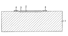
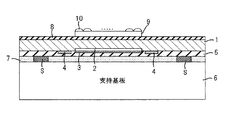
本実施形態の裏面照射型撮像素子の概略構成は、図7に示すような構成であり、半導体基板の一例であるシリコン基板1の表面側には、シリコン基板1で発生した電荷を蓄積するための多数の電荷蓄積領域や各電荷蓄積領域に蓄積された電荷を転送するCCDを構成する転送チャネル等の素子構造物2、転送チャネルを駆動する駆動電極や各種配線等の素子構造物3、電極パッド4、及びこれらを保護する保護層や平坦化層として機能する絶縁層5等を含む表面側素子構成層が形成されている。又、シリコン基板1の裏面側には、平坦化層8、各電荷蓄積領域に入射させる光を分光するカラーフィルタ9、及び各電荷蓄積領域に光を集光するためのマイクロレンズ10等を含む裏面側素子構成層が形成されている。表面側素子構成層にはスペーサSの一端が接触し、スペーサSの他端には支持基板6が接触している。そして、表面側素子構成層と支持基板6との間の空間には接着材7が充填されており、これによってシリコン基板1と支持基板6とが貼りあわされている。
(First embodiment)
1-7 is a cross-sectional schematic diagram in each process of the manufacturing process of the back irradiation type image pick-up element which is 1st embodiment of this invention.
The schematic configuration of the back-illuminated image sensor according to the present embodiment is as shown in FIG. 7, and charges generated on the
図7に示す裏面照射型撮像素子は、シリコン基板1の裏面側から光を入射して用いるものである。マイクロレンズ10で集光され、カラーフィルタ9で分光された光はシリコン基板1に入射する。そして、ここで発生した電荷は電荷蓄積領域に蓄積され、CCDによって転送された電荷がアンプによって外部に出力される。本明細書では、シリコン基板1の表面及び裏面を規準として、各構成要素の位置関係を定義するものとする。例えば、シリコン基板1の表面を規準としたときは、光の入射方向を該表面の上方向と定義し、シリコン基板1の裏面を規準としたときは、光の入射方向とは反対方向を該裏面の上方向と定義する。
The backside illumination type imaging device shown in FIG. 7 is used by making light incident from the backside of the
このような定義にしたがい、本実施形態の裏面照射型撮像素子は、シリコン基板1と、シリコン基板1の表面上に形成された表面側素子構成層(素子構造物3,電極パッド4、絶縁層5)と、表面側素子構成層の絶縁層5上方に形成されたガラス等の支持基板6と、表面側素子構成層の絶縁層5に一端が接触し、支持基板6に他端が接触したスペーサSと、スペーサSによって形成された絶縁層5と支持基板6との間の空間に充填された接着材7と、シリコン基板1の裏面上に形成された平坦化層8、平坦化層8上に形成されたカラーフィルタ9、及びカラーフィルタ9上に形成されたマイクロレンズ10を含む裏面側素子構成層とを備えた構成となっている。
In accordance with such a definition, the back-illuminated image sensor according to the present embodiment includes a
以下、このような構成の裏面照射型撮像素子の製造方法を図1〜図7を参照して説明する。
まず、図1に示すように、シリコン基板1表面を上にして固定し、表面内に素子構造物2を形成し、表面上に素子構造物3や電極パッド4を公知のプロセスによって形成する。次に、図2に示すように、シリコン基板1表面上に絶縁材料を成膜後、これを平坦化して絶縁層5を形成する。
Hereinafter, a manufacturing method of the backside illumination type imaging device having such a configuration will be described with reference to FIGS.
First, as shown in FIG. 1, the surface of the
次に、図3に示すように、支持基板6を用意し、支持基板6上に支持基板6とは異なる材料(例えば金属材料)をCVDやPVD法等の膜厚均一性のよい成膜方法で成膜し、その上の特定の位置にのみレジストパターンRを露光及び現像工程(フォトリソグラフィ)によって形成する。次に、図4に示すように、レジストパターンRをマスクにして金属材料膜Zのエッチングを行い、レジストパターンR下方の金属材料7以外を除去して、スペーサSを形成する。尚、支持基板6にスペーサSを形成する工程は、図2に示す状態の素子を作る前に行っておいても良いし、同時に行っても良い。
Next, as shown in FIG. 3, a
このスペーサSは、シリコン基板1と支持基板6の間の空間の厚みを均一にするためのものである。このため、スペーサSは、シリコン基板1の表面側素子構成層にスペーサSを介して支持基板6を接触させたときに、双方が安定して平行になる程度の数及び位置を適宜決めておけば良い。
This spacer S is for making the thickness of the space between the
次に、図5に示すように、スペーサSの支持基板6との接触面とは反対面にシリコン基板1の絶縁層5が接触するように、該反対面上にシリコン基板1を載置する。スペーサSは、CVDやPVD法等の膜厚均一性のよい成膜方法で成膜した材料をフォトリソグラフィ及びエッチングによってパターニングすることで形成されているため、その高さは均一となっている。一方で、スペーサSが接触する絶縁層5の面は平坦化されている、つまり、該面はシリコン基板1表面からの距離が均一な面となっている。このため、図5に示した状態で、シリコン基板1と支持基板6との間の空間の厚みはどの場所においても均一なものとなる。そして、この状態でシリコン基板1の裏面から圧力をかけながら、スペーサSによって形成された絶縁層5と支持基板6との間の空間に、接着材として有機材料の接着材(例えばエポキシ樹脂)7を充填することで、シリコン基板1と支持基板6とを貼り合わせる。
Next, as shown in FIG. 5, the
尚、接着材7は、シリコン基板1と支持基板6とが貼り合わされれば充分であるため、絶縁層5と支持基板6との間の空間の全てに充填しなくても良く、この空間の少なくとも一部に充填しておけば良い。
Note that the adhesive 7 is sufficient if the
次に、図6に示すように、支持基板6を固定した状態で、シリコン基板1の厚みが例えば10μm程度となるまでシリコン基板1を裏面側からエッチングする。次に、図7に示すように、樹脂等の絶縁材料をシリコン基板1の裏面上に成膜して平坦化層8を形成する。次に、平坦化層8上に、カラーフィルタ9を公知のプロセスによって形成し、カラーフィルタ9上にマイクロレンズ10を公知のプロセスによって形成する。そして、図7に示した構成の素子をパッケージングして、裏面照射型撮像素子の製造を完了する。
Next, as shown in FIG. 6, with the
以上のような方法によれば、シリコン基板1と支持基板6との距離がどの場所でもほぼ均一となっているため、特許文献1に示した素子と比べて、裏面側素子構成層の各構成要素の位置及び形状の精度を向上させることができる。したがって、素子特性の向上、歩留まりの向上、及び混色の低減等を実現することが可能となる。
According to the method as described above, since the distance between the
尚、本実施形態では、表面側素子構成層の表面が平坦となっているが、これが平坦になっていない場合も有りうる。この場合は、表面側素子構成層を形成するときに、例えば図8に示すように、表面側素子構成層の表面の特定の位置にシリコン基板1の表面からの距離が均一となる面15が形成されるように、表面側素子構成層内の構造を設計しておけば良い。そして、図9に示すように、支持基板6に形成したスペーサSが面15に接触するように、支持基板6のスペーサS上にシリコン基板1を載置し、圧力をかけながら接着材7を充填して貼り合わせを行えば良い。
In the present embodiment, the surface of the surface-side element constituent layer is flat. However, this may not be flat. In this case, when the surface-side element constituent layer is formed, for example, as shown in FIG. 8, a
図10は、シリコン基板及び支持基板の全体を示した平面模式図であり、(a)はシリコン基板1を表面側から見た図であり、(b)は支持基板6をスペーサSの形成面側から見た図である。
図10(a)に示すように、裏面照射型撮像素子を形成すべき領域であるチップ領域Cの中央に表面側素子構成層16を形成した場合には、それを取り囲むように面15を形成しておき、支持基板6には、図10(b)に示すように、面15に対応する位置にスペーサSを形成しておく。そして、図10(a)に示したシリコン基板1と図10(b)に示した支持基板6とを貼り合わせて接着することで、シリコン基板1と支持基板6とを平行にすることができる。
FIG. 10 is a schematic plan view showing the whole of the silicon substrate and the support substrate, (a) is a view of the
As shown in FIG. 10A, in the case where the front side
(第二実施形態)
図11〜図15は、本発明の第二実施形態である裏面照射型撮像素子の製造工程の各工程における断面模式図である。
まず、第一実施形態で説明した方法と同様の方法で図2に示した状態の素子を形成する。次に、図11に示すように、絶縁層5上の特定の位置にフォトリソグラフィ及びエッチングによってスペーサS’(凸部のパターン)を形成する。つまり、絶縁層5上に絶縁層5とは異なる材料(例えば金属材料)をCVDやPVD法等の膜厚均一性のよい成膜方法で成膜し、金属材料膜上に露光及び現像工程によってレジストのマスクパターンを形成し、このマスクパターンを介して金属材料膜をエッチングすることで、スペーサS’を形成する。
(Second embodiment)
FIGS. 11-15 is a cross-sectional schematic diagram in each process of the manufacturing process of the back irradiation type image pick-up element which is 2nd embodiment of this invention.
First, the element in the state shown in FIG. 2 is formed by a method similar to the method described in the first embodiment. Next, as shown in FIG. 11, a spacer S ′ (projection pattern) is formed at a specific position on the insulating
次に、図12に示すように、スペーサS’の絶縁層5との接触面とは反対面にガラス等の支持基板6’が接触するように、該反対面上に支持基板6’を載置する。スペーサS’はCVDやPVD法等の膜厚均一性のよい成膜方法で成膜した膜をフォトリソグラフィ及びエッチングによってパターニングすることで形成されているため、その高さは均一となっている。又、スペーサS’が接触する絶縁層5の面は平坦化されている、つまり、該面はシリコン基板1表面からの距離が均一な面となっている。このため、図12に示した状態で、シリコン基板1と支持基板6’との間の空間の厚みはどの場所においても均一なものとなる。そして、この状態で支持基板6’に圧力をかけながら、スペーサS’によって形成された絶縁層5と支持基板6’との間の空間に、接着材として有機材料の接着材(例えばエポキシ樹脂)7’を充填することで、シリコン基板1と支持基板6’とを貼り合わせる。
Next, as shown in FIG. 12, the
尚、接着材7は、シリコン基板1と支持基板6’とが貼り合わされれば充分であるため、絶縁層5と支持基板6’との間の空間の全てに充填しなくても良く、この空間の少なくとも一部に充填しておけば良い。
The adhesive 7 is sufficient if the
このスペーサS’は、スペーサSと同様、シリコン基板1と支持基板6’の間の空間の厚みを均一にするためのものである。このため、スペーサS’は、シリコン基板1と支持基板6’とをスペーサS’を介して接触させたときに、双方が安定して平行になる程度の数及び位置を適宜決めておけば良い。
Like the spacer S, the spacer S ′ is for making the thickness of the space between the
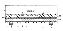
次に、第一実施形態で説明した方法と同様に、シリコン基板1の裏面をエッチングして厚みを10μmとし、シリコン基板1の裏面上に平坦化層8を形成し、平坦化層8上にカラーフィルタ9を形成し、カラーフィルタ9上にマイクロレンズ10を形成する。次に、図13に示すように、カラーフィルタ9及びマイクロレンズ10を保護するための透明な樹脂材料等からなる保護層11を形成し、保護層11上に有機材料の接着材を塗布し、この接着材を介して、保護層11にガラス等の透明基板12を貼り付ける。
Next, similarly to the method described in the first embodiment, the back surface of the
次に、図14に示すように、支持基板6’を接着材7’と共に絶縁層5から剥離する。次に、図15に示すように、裏面照射型撮像素子を収容するためのパッケージ本体又は裏面照射型撮像素子を駆動する駆動回路や信号処理回路が作りこまれた回路基板等の実装基体14を用意し、実装基体14にスペーサS’を接触させた状態で、スペーサS’によって形成された絶縁層5と実装基体14との間の空間に接着材として有機材料の接着材(例えばエポキシ樹脂)13を充填することで、シリコン基板1を実装基体14に接着する。
Next, as shown in FIG. 14, the
尚、接着材13は、シリコン基板1と実装基体14とが接着されれば充分であるため、絶縁層5と実装基体14との間の空間の全てに充填しなくても良く、この空間の少なくとも一部に充填しておけば良い。
The adhesive 13 is sufficient if the
以上のような方法によれば、シリコン基板1と支持基板6’との距離がどの場所でもほぼ均一となった状態で裏面側素子構成層を形成することができるため、特許文献1に示した素子と比べて、裏面側素子構成層の各構成要素の位置及び形状の精度を向上させることができる。したがって、素子特性の向上、歩留まりの向上、及び混色の低減等を実現することが可能となる。
According to the above method, since the back surface side element constituting layer can be formed in a state where the distance between the
又、以上のような方法によれば、シリコン基板1と実装基体14とを、スペーサS’を介して接着材13により接着することができるため、シリコン基板1を実装基体14の素子載置面に対して平行にすることができ、裏面照射型撮像素子をカメラに実装した場合のカメラ光学系とのずれ等をなくすことができる。
Further, according to the above method, the
尚、図13に示した状態の素子を形成後、この素子をパッケージングして裏面照射型撮像素子を完成させることも可能であるが、この場合、支持基板6’を実装基体に接着する際に、支持基板6’が実装基体の素子載置面に対して傾いてしまう恐れがある。このような事態を回避するために上述した方法を採用することは有効である。
It is possible to complete the back-illuminated image pickup device after forming the device in the state shown in FIG. 13, but in this case, when the
又、本実施形態においても、表面側素子構成層の表面が平坦となっていない場合は、表面側素子構成層を形成するときに、例えば図8に示すように、表面側素子構成層の表面の特定の位置にシリコン基板1の表面からの距離が均一となる面15が形成されるように、表面側素子構成層内の構造を設計しておき、面15上にスペーサS’を形成する方法を採用すれば良い。
Also in this embodiment, when the surface of the surface side element constituent layer is not flat, when the surface side element constituent layer is formed, as shown in FIG. The structure in the surface side element constituting layer is designed so that the
第一実施形態及び第二実施形態では、裏面照射型撮像素子がCCD型である例を示したが、CMOS型であっても良い。この場合は、表面側素子構成層をCMOS型に必要な素子からなる層とすれば良い。 In the first embodiment and the second embodiment, an example in which the back-illuminated imaging element is a CCD type is shown, but a CMOS type may be used. In this case, the surface side element constituent layer may be a layer made of elements necessary for the CMOS type.
1 シリコン基板
2,3,4,5 表面側素子構成層
6 支持基板
7 接着材
8,9,10 裏面側素子構成層
S スペーサ
DESCRIPTION OF
Claims (6)
前記半導体基板の裏面上に形成された前記裏面側の素子を構成する裏面側素子構成層と、
前記半導体基板の表面上に形成された前記表面側の素子を構成する表面側素子構成層と、
前記表面側素子構成層上方に形成された支持基板と、
前記半導体基板と前記支持基板との間隔を均一にするためのスペーサであって、前記表面側素子構成層に一端が接触し、前記支持基板に他端が接触する複数のスペーサと、
前記複数のスペーサによって形成された前記表面側素子構成層と前記支持基板との間の空間の少なくとも一部に充填された接着材とを備え、
前記複数のスペーサは、前記表面側素子構成層上又は前記支持基板上に成膜された材料をフォトリソグラフィ及びエッチングによってパターニングして形成されたものであり、
前記表面側素子構成層表面には、前記複数のスペーサの各々と対応する位置に前記半導体基板の表面からの距離が均一な底面を有する複数の凹部が形成され、
前記スペーサの一端が当該スペーサに対応する位置の前記凹部の底面に接触している裏面照射型撮像素子。 A backside-illuminated imaging device that irradiates light from the back side of a semiconductor substrate, reads out charges generated in the semiconductor substrate in response to the light from the front side of the semiconductor substrate, and performs imaging,
A back side element constituting layer constituting the element on the back side formed on the back side of the semiconductor substrate;
A surface-side element constituting layer constituting the surface-side element formed on the surface of the semiconductor substrate;
A support substrate formed above the surface-side element constituent layer;
A spacer for a uniform gap between the supporting substrate and the semiconductor substrate, one end is in contact with the surface element constituent layers, and a plurality of spacers that contacts the other end to the support substrate,
An adhesive filled in at least a part of a space between the surface-side element constituent layer formed by the plurality of spacers and the support substrate;
Wherein the plurality of spacers state, and are not the has been formed on the surface side device structure layer or the supporting substrate material is formed by patterning by photolithography and etching,
A plurality of recesses having a bottom surface with a uniform distance from the surface of the semiconductor substrate is formed at a position corresponding to each of the plurality of spacers on the surface-side element constituent layer surface,
A back-illuminated image sensor in which one end of the spacer is in contact with the bottom surface of the recess at a position corresponding to the spacer .
前記支持基板が前記裏面照射型撮像素子の実装基体である裏面照射型撮像素子。 The back-illuminated image sensor according to claim 1,
A backside-illuminated image sensor, wherein the support substrate is a mounting substrate for the backside-illuminated image sensor.
前記半導体基板の表面上に、前記表面側の素子を構成する表面側素子構成層を形成する表面側素子構成層形成工程と、 On the surface of the semiconductor substrate, a surface-side element constituent layer forming step for forming a surface-side element constituent layer constituting the surface-side element;
前記半導体基板を支持するための支持基板を用意し、前記支持基板上に材料を成膜し、成膜した材料をフォトリソグラフィ及びエッチングによってパターニングして前記支持基板上の特定の位置に複数の凸部を形成する凸部形成工程と、 A support substrate for supporting the semiconductor substrate is prepared, a material is formed on the support substrate, and the formed material is patterned by photolithography and etching to form a plurality of protrusions at specific positions on the support substrate. A convex portion forming step for forming a portion;
前記複数の凸部を前記表面側素子構成層に接触させた状態で、前記複数の凸部によって形成された前記表面側素子構成層と前記支持基板との間の空間の少なくとも一部に接着材を充填して、前記半導体基板と前記支持基板を貼り合わせる貼り合わせ工程と、 In a state where the plurality of convex portions are in contact with the surface-side element constituent layer, an adhesive is applied to at least a part of the space between the surface-side element constituent layer and the support substrate formed by the plurality of convex portions. A bonding step of bonding the semiconductor substrate and the support substrate;
前記支持基板と前記半導体基板を貼り合わせた状態で、前記半導体基板の裏面上に前記裏面側の素子を構成する裏面側素子構成層を形成する裏面側素子構成層形成工程とを備え、 In the state where the support substrate and the semiconductor substrate are bonded together, a back side element constituent layer forming step of forming a back side element constituent layer that constitutes the back side element on the back side of the semiconductor substrate,
前記表面側素子構成層形成工程では、前記表面側素子構成層表面の前記特定の位置と対応する位置に、前記半導体基板の表面からの距離が均一な底面を有する凹部を形成し、 In the surface-side element constituent layer forming step, a recess having a bottom surface with a uniform distance from the surface of the semiconductor substrate is formed at a position corresponding to the specific position on the surface-side element constituent layer surface;
前記貼り合わせ工程では、前記凸部を前記凹部の底面に接触させた状態で接着材の充填を行う裏面照射型撮像素子の製造方法。 In the bonding step, a method of manufacturing a backside illuminating type imaging device in which the adhesive is filled in a state where the convex portion is in contact with the bottom surface of the concave portion.
前記半導体基板の表面上に前記表面側の素子を構成する表面側素子構成層であって、表面の特定の位置に、前記半導体基板の表面からの距離が均一な底面を有する複数の凹部を有する表面側素子構成層を形成する表面側素子構成層形成工程と、
前記表面側素子構成層上に材料を成膜し、成膜した材料をフォトリソグラフィ及びエッチングによってパターニングして、前記表面側素子構成層の前記複数の凹部の各々の底面上に凸部を形成する凸部形成工程と、
前記半導体基板を支持するための支持基板を用意し、前記支持基板に前記複数の凸部を接触させた状態で、前記複数の凸部によって形成された前記表面側素子構成層と前記支持基板との間の空間の少なくとも一部に接着材を充填して、前記半導体基板と前記支持基板を貼り合わせる貼り合わせ工程と、
前記支持基板と前記半導体基板を貼り合わせた状態で、前記半導体基板の裏面上に前記裏面側の素子を構成する裏面側素子構成層を形成する裏面側素子構成層形成工程とを備える裏面照射型撮像素子の製造方法。 A method of manufacturing a backside illuminated imaging device that irradiates light from the back side of a semiconductor substrate, reads out charges generated in the semiconductor substrate in response to the light from the front side of the semiconductor substrate, and performs imaging,
A surface-side element constituting layer that constitutes the surface-side element on the surface of the semiconductor substrate, and has a plurality of recesses having a bottom surface that is uniformly spaced from the surface of the semiconductor substrate at a specific position on the surface. the surface-side device structure layer forming step of forming a surface-side device structure layer,
A material is formed on the surface-side element constituent layer, and the formed material is patterned by photolithography and etching to form a convex portion on the bottom surface of each of the plurality of concave portions of the surface-side element constituent layer. A convex forming step;
A support substrate for supporting the semiconductor substrate is prepared, and the surface-side element constituting layer formed by the plurality of protrusions and the support substrate in a state where the plurality of protrusions are in contact with the support substrate. A bonding step of filling at least a part of the space between the adhesive and bonding the semiconductor substrate and the support substrate;
A backside irradiation type comprising a backside element constituent layer forming step of forming a backside element constituent layer constituting the backside element on the backside of the semiconductor substrate in a state where the support substrate and the semiconductor substrate are bonded together. Manufacturing method of imaging device.
前記裏面側素子構成層形成工程の後、前記支持基板を前記接着材と共に前記表面側素子構成層から剥離する支持基板剥離工程と、 前記裏面照射型撮像素子の実装基体を用意し、前記実装基体に前記複数の凸部を接触させた状態で、前記複数の凸部によって形成された前記表面側素子構成層と前記実装基体との間の空間の少なくとも一部に接着材を充填して、前記半導体基板と前記実装基体を接着する工程とを備える裏面照射型撮像素子の製造方法。 It is a manufacturing method of the back irradiation type image sensor according to claim 4,
After the back side element constituent layer forming step, a support substrate peeling step for peeling the support substrate together with the adhesive from the front side element constituent layer; and a mounting base for the back side illumination type imaging device are prepared, and the mounting base In a state where the plurality of protrusions are in contact with each other, an adhesive is filled in at least a part of the space between the surface-side element constituent layer formed by the plurality of protrusions and the mounting substrate, A method of manufacturing a backside illuminating type imaging device comprising a step of bonding a semiconductor substrate and the mounting substrate .
前記半導体基板の表面上に前記表面側の素子を構成する表面側素子構成層であって表面が平坦な表面側素子構成層を形成する表面側素子構成層形成工程と、
前記表面側素子構成層上に材料を成膜し、成膜した材料をフォトリソグラフィ及びエッチングによってパターニングして前記表面側素子構成層上に複数の凸部を形成する凸部形成工程と、
前記半導体基板を支持するための支持基板を用意し、前記支持基板に前記複数の凸部を接触させた状態で、前記複数の凸部によって形成された前記表面側素子構成層と前記支持基板との間の空間の少なくとも一部に接着材を充填して、前記半導体基板と前記支持基板を貼り合わせる貼り合わせ工程と、
前記支持基板と前記半導体基板を貼り合わせた状態で、前記半導体基板の裏面上に前記裏面側の素子を構成する裏面側素子構成層を形成する裏面側素子構成層形成工程と、
前記裏面側素子構成層形成工程の後、前記支持基板を前記接着材と共に前記表面側素子構成層から剥離する支持基板剥離工程と、 前記裏面照射型撮像素子の実装基体を用意し、前記実装基体に前記複数の凸部を接触させた状態で、前記複数の凸部によって形成された前記表面側素子構成層と前記実装基体との間の空間の少なくとも一部に接着材を充填して、前記半導体基板と前記実装基体を接着する工程とを備える裏面照射型撮像素子の製造方法。 A method of manufacturing a backside illuminated imaging device that irradiates light from the back side of a semiconductor substrate, reads out charges generated in the semiconductor substrate in response to the light from the front side of the semiconductor substrate, and performs imaging,
A surface-side element constituent layer forming step of forming a surface-side element constituent layer that is a surface-side element constituent layer that constitutes the surface-side element on the surface of the semiconductor substrate;
Forming a material on the surface-side element constituent layer, patterning the deposited material by photolithography and etching, and forming a plurality of convex parts on the surface-side element constituent layer; and
A support substrate for supporting the semiconductor substrate is prepared, and the surface-side element constituting layer formed by the plurality of protrusions and the support substrate in a state where the plurality of protrusions are in contact with the support substrate. A bonding step of filling at least a part of the space between the adhesive and bonding the semiconductor substrate and the support substrate;
In a state where the support substrate and the semiconductor substrate are bonded together, a back side element constituent layer forming step for forming a back side element constituent layer constituting the back side element on the back side of the semiconductor substrate;
After the back side element constituent layer forming step, a support substrate peeling step for peeling the support substrate together with the adhesive from the front side element constituent layer; and a mounting base for the back side illumination type imaging device are prepared, and the mounting base In a state where the plurality of protrusions are in contact with each other, an adhesive is filled in at least a part of the space between the surface-side element constituent layer formed by the plurality of protrusions and the mounting substrate, A method of manufacturing a backside illuminating type imaging device comprising a step of bonding a semiconductor substrate and the mounting substrate .
Priority Applications (3)
| Application Number | Priority Date | Filing Date | Title |
|---|---|---|---|
| JP2007143804A JP4644696B2 (en) | 2007-05-30 | 2007-05-30 | Back-illuminated image sensor and manufacturing method thereof |
| US12/126,592 US7893516B2 (en) | 2007-05-30 | 2008-05-23 | Backside-illuminated imaging device and manufacturing method of the same |
| US13/007,482 US8158452B2 (en) | 2007-05-30 | 2011-01-14 | Backside-illuminated imaging device and manufacturing method of the same |
Applications Claiming Priority (1)
| Application Number | Priority Date | Filing Date | Title |
|---|---|---|---|
| JP2007143804A JP4644696B2 (en) | 2007-05-30 | 2007-05-30 | Back-illuminated image sensor and manufacturing method thereof |
Publications (3)
| Publication Number | Publication Date |
|---|---|
| JP2008300551A JP2008300551A (en) | 2008-12-11 |
| JP2008300551A5 JP2008300551A5 (en) | 2010-08-26 |
| JP4644696B2 true JP4644696B2 (en) | 2011-03-02 |
Family
ID=40087184
Family Applications (1)
| Application Number | Title | Priority Date | Filing Date |
|---|---|---|---|
| JP2007143804A Expired - Fee Related JP4644696B2 (en) | 2007-05-30 | 2007-05-30 | Back-illuminated image sensor and manufacturing method thereof |
Country Status (2)
| Country | Link |
|---|---|
| US (2) | US7893516B2 (en) |
| JP (1) | JP4644696B2 (en) |
Families Citing this family (3)
| Publication number | Priority date | Publication date | Assignee | Title |
|---|---|---|---|---|
| JP5644096B2 (en) | 2009-11-30 | 2014-12-24 | ソニー株式会社 | Method for manufacturing bonded substrate and method for manufacturing solid-state imaging device |
| JP2013175540A (en) * | 2012-02-24 | 2013-09-05 | Nikon Corp | Solid state image pickup device and manufacturing method of the same |
| JP6328025B2 (en) * | 2014-10-10 | 2018-05-23 | キヤノン株式会社 | Silicon substrate processing method, liquid discharge head substrate manufacturing method, and liquid discharge head manufacturing method |
Citations (4)
| Publication number | Priority date | Publication date | Assignee | Title |
|---|---|---|---|---|
| JPH1167823A (en) * | 1997-08-08 | 1999-03-09 | Hitachi Chem Co Ltd | Manufacture of wiring board with bump and semiconductor package |
| WO2000062344A1 (en) * | 1999-04-13 | 2000-10-19 | Hamamatsu Photonics K.K. | Semiconductor device |
| JP2001308092A (en) * | 2000-04-18 | 2001-11-02 | Toyo Kohan Co Ltd | Multilayered metal plate used for forming interconnection on semiconductor wafer, and method for forming the interconnection on semiconductor wafer |
| JP2004296825A (en) * | 2003-03-27 | 2004-10-21 | Hamamatsu Photonics Kk | Photo diode array, its manufacturing method and radiation detector |
Family Cites Families (4)
| Publication number | Priority date | Publication date | Assignee | Title |
|---|---|---|---|---|
| JPH06350068A (en) | 1993-06-03 | 1994-12-22 | Hamamatsu Photonics Kk | Manufacture of semiconductor energy ray detector |
| AU2003235925A1 (en) | 2002-05-10 | 2003-11-11 | Hamamatsu Photonics K.K. | Rear surface irradiation photodiode array and method for producing the same |
| JP4389626B2 (en) | 2004-03-29 | 2009-12-24 | ソニー株式会社 | Manufacturing method of solid-state imaging device |
| JP4720120B2 (en) | 2004-07-14 | 2011-07-13 | ソニー株式会社 | Semiconductor image sensor module |
-
2007
- 2007-05-30 JP JP2007143804A patent/JP4644696B2/en not_active Expired - Fee Related
-
2008
- 2008-05-23 US US12/126,592 patent/US7893516B2/en not_active Expired - Fee Related
-
2011
- 2011-01-14 US US13/007,482 patent/US8158452B2/en not_active Expired - Fee Related
Patent Citations (4)
| Publication number | Priority date | Publication date | Assignee | Title |
|---|---|---|---|---|
| JPH1167823A (en) * | 1997-08-08 | 1999-03-09 | Hitachi Chem Co Ltd | Manufacture of wiring board with bump and semiconductor package |
| WO2000062344A1 (en) * | 1999-04-13 | 2000-10-19 | Hamamatsu Photonics K.K. | Semiconductor device |
| JP2001308092A (en) * | 2000-04-18 | 2001-11-02 | Toyo Kohan Co Ltd | Multilayered metal plate used for forming interconnection on semiconductor wafer, and method for forming the interconnection on semiconductor wafer |
| JP2004296825A (en) * | 2003-03-27 | 2004-10-21 | Hamamatsu Photonics Kk | Photo diode array, its manufacturing method and radiation detector |
Also Published As
| Publication number | Publication date |
|---|---|
| US20110111547A1 (en) | 2011-05-12 |
| JP2008300551A (en) | 2008-12-11 |
| US20080296720A1 (en) | 2008-12-04 |
| US8158452B2 (en) | 2012-04-17 |
| US7893516B2 (en) | 2011-02-22 |
Similar Documents
| Publication | Publication Date | Title |
|---|---|---|
| JP4501130B2 (en) | Imaging device and manufacturing method thereof | |
| TWI488499B (en) | Method and apparatus for lens alignment for optically sensitive devices and systems implementing same | |
| TWI463645B (en) | Cfa alignment mark formation in image sensors | |
| JP5317586B2 (en) | Camera module and manufacturing method thereof | |
| JP3778817B2 (en) | Solid-state imaging device and manufacturing method thereof | |
| TWI721378B (en) | Image sensor package and manufacturing method of the same | |
| JP2006228837A (en) | Semiconductor device and its manufacturing method | |
| JP5721370B2 (en) | Manufacturing method of optical sensor, optical sensor and camera | |
| US8193025B2 (en) | Photomask, image sensor, and method of manufacturing the image sensor | |
| US8048768B2 (en) | Joined wafer, fabrication method thereof, and fabrication method of semiconductor devices | |
| US20170062504A1 (en) | Semiconductor device with surface integrated focusing element and method of producing a semiconductor device with focusing element | |
| JP2008052004A (en) | Lens array and method for manufacturing solid-state image pickup element | |
| JP5342838B2 (en) | Camera module and manufacturing method thereof | |
| JP2004063751A (en) | Solid-state image sensing device and its manufacturing method | |
| JP4174247B2 (en) | Manufacturing method of solid-state imaging device | |
| JP4644696B2 (en) | Back-illuminated image sensor and manufacturing method thereof | |
| JP2009176949A (en) | Backside irradiation-type solid state image pickup device and its production process | |
| JP2004063782A (en) | Solid-state image sensing device and its manufacturing method | |
| JP2011009389A (en) | Solid-state image pickup device and manufacturing method thereof | |
| JP5564751B2 (en) | Manufacturing method of image sensor | |
| JP2006190944A (en) | Image sensor die | |
| JP2012099639A (en) | Image sensor and method of manufacturing the same | |
| JP2001358320A (en) | Solid state image sensor and its manufacturing method as well as method for manufacturing on-chip lens mold | |
| JP5047077B2 (en) | Method for manufacturing solid-state imaging device | |
| CN111009542A (en) | Packaging method and packaging structure |
Legal Events
| Date | Code | Title | Description |
|---|---|---|---|
| A621 | Written request for application examination |
Free format text: JAPANESE INTERMEDIATE CODE: A621 Effective date: 20100212 |
|
| A521 | Request for written amendment filed |
Free format text: JAPANESE INTERMEDIATE CODE: A523 Effective date: 20100712 |
|
| A871 | Explanation of circumstances concerning accelerated examination |
Free format text: JAPANESE INTERMEDIATE CODE: A871 Effective date: 20100712 |
|
| A975 | Report on accelerated examination |
Free format text: JAPANESE INTERMEDIATE CODE: A971005 Effective date: 20100730 |
|
| A131 | Notification of reasons for refusal |
Free format text: JAPANESE INTERMEDIATE CODE: A131 Effective date: 20100810 |
|
| A521 | Request for written amendment filed |
Free format text: JAPANESE INTERMEDIATE CODE: A523 Effective date: 20100921 |
|
| TRDD | Decision of grant or rejection written | ||
| A01 | Written decision to grant a patent or to grant a registration (utility model) |
Free format text: JAPANESE INTERMEDIATE CODE: A01 Effective date: 20101109 |
|
| A01 | Written decision to grant a patent or to grant a registration (utility model) |
Free format text: JAPANESE INTERMEDIATE CODE: A01 |
|
| A61 | First payment of annual fees (during grant procedure) |
Free format text: JAPANESE INTERMEDIATE CODE: A61 Effective date: 20101206 |
|
| R150 | Certificate of patent or registration of utility model |
Ref document number: 4644696 Country of ref document: JP Free format text: JAPANESE INTERMEDIATE CODE: R150 Free format text: JAPANESE INTERMEDIATE CODE: R150 |
|
| FPAY | Renewal fee payment (event date is renewal date of database) |
Free format text: PAYMENT UNTIL: 20131210 Year of fee payment: 3 |
|
| R250 | Receipt of annual fees |
Free format text: JAPANESE INTERMEDIATE CODE: R250 |
|
| R250 | Receipt of annual fees |
Free format text: JAPANESE INTERMEDIATE CODE: R250 |
|
| R250 | Receipt of annual fees |
Free format text: JAPANESE INTERMEDIATE CODE: R250 |
|
| R250 | Receipt of annual fees |
Free format text: JAPANESE INTERMEDIATE CODE: R250 |
|
| R250 | Receipt of annual fees |
Free format text: JAPANESE INTERMEDIATE CODE: R250 |
|
| LAPS | Cancellation because of no payment of annual fees |