JP4635687B2 - DATA ACCESS DEVICE, DATA ACCESS METHOD, PROGRAM, AND RECORDING MEDIUM - Google Patents
DATA ACCESS DEVICE, DATA ACCESS METHOD, PROGRAM, AND RECORDING MEDIUM Download PDFInfo
- Publication number
- JP4635687B2 JP4635687B2 JP2005099835A JP2005099835A JP4635687B2 JP 4635687 B2 JP4635687 B2 JP 4635687B2 JP 2005099835 A JP2005099835 A JP 2005099835A JP 2005099835 A JP2005099835 A JP 2005099835A JP 4635687 B2 JP4635687 B2 JP 4635687B2
- Authority
- JP
- Japan
- Prior art keywords
- address
- pixel
- read
- data
- write
- Prior art date
- Legal status (The legal status is an assumption and is not a legal conclusion. Google has not performed a legal analysis and makes no representation as to the accuracy of the status listed.)
- Expired - Fee Related
Links
Images


Landscapes
- Image Input (AREA)
- Image Processing (AREA)
Description
この発明は、所定画面上に設定される複数の画素のパターンをアクセスパターンとし、このアクセスパターンの設定位置を開始位置から画素列方向に順次移動した各設定位置で、このアクセスパターンで特定される複数の画素の画素データを同時に取得するデータアクセス装置、データアクセス方法、プログラムおよび記録媒体に関する。 In the present invention, a pattern of a plurality of pixels set on a predetermined screen is used as an access pattern, and the setting position of the access pattern is specified by the access pattern at each setting position sequentially moved in the pixel column direction from the start position. The present invention relates to a data access device, a data access method, a program, and a recording medium that simultaneously acquire pixel data of a plurality of pixels.
詳しくは、この発明は、アクセスパターンの設定位置を開始位置から画素列方向に順次移動した各設定位置で、当該アクセスパターンで特定される複数の画素の画素データがそれぞれ異なるメモリバンクに格納された状態として、当該複数の画素データを同時にアクセスできるようにしたことによって、当該複数の画素データの同時取得を容易としたデータアクセス装置等に係るものである。 Specifically, according to the present invention, pixel data of a plurality of pixels specified by the access pattern are stored in different memory banks at each setting position where the access pattern setting position is sequentially moved in the pixel column direction from the start position. The present invention relates to a data access device that facilitates simultaneous acquisition of the plurality of pixel data by allowing the plurality of pixel data to be accessed simultaneously.
従来、半導体メモリMYは、図16に示すように、ワード線WLとビット線BLを指定してメモリセルMCをアクセスする構造となっており、指定されたワード線WLとビット線BLが交差する位置にあるメモリセルMCに格納されたデータが読み出される。このような構造の半導体メモリMYでは、複数のワード線WLで同じビット線BLを共有している。したがって、図17のように、例えば2つのワード線WL1,WL2を指定すると、ビット線BLにはこれらワード線WL1,WL2のデータが混じり合って出てくるため、異なるワード線WLのデータには同時アクセスできない。 Conventionally, as shown in FIG. 16, the semiconductor memory MY has a structure in which a memory cell MC is accessed by designating a word line WL and a bit line BL, and the designated word line WL and the bit line BL intersect. Data stored in the memory cell MC at the position is read out. In the semiconductor memory MY having such a structure, a plurality of word lines WL share the same bit line BL. Therefore, as shown in FIG. 17, for example, when two word lines WL1 and WL2 are designated, the data of these word lines WL1 and WL2 are mixedly output on the bit line BL. Simultaneous access is not possible.
これに対して、図18のように、メモリMYを複数のメモリバンクBK0〜BKn−1に分け、それぞれのメモリバンクBK0〜BKn−1に異なるアドレスを指定することで、複数のワード線WLのデータに同時にアクセスできるが、メモリバンク内の異なるワード線WLのデータには同時にアクセスできない。 On the other hand, as shown in FIG. 18, the memory MY is divided into a plurality of memory banks BK0 to BKn-1, and different addresses are assigned to the memory banks BK0 to BKn-1, so Data can be accessed simultaneously, but data on different word lines WL in the memory bank cannot be accessed simultaneously.
一般に、同時に複数データにアクセスが可能なのは、その複数データが異なるメモリバンクに格納されているか、あるいはその複数データが同一ワード線上に格納されているかのいずれかである。 In general, a plurality of data can be accessed at the same time either by storing the plurality of data in different memory banks or by storing the plurality of data on the same word line.
また従来、入力データに含まれる特定のデータ配列を認識することにより、パターン認識や動き検出等の処理が行われている。例えば、数ラインの画素データを蓄積でき画素単位で出力できるバッファメモリと、数ビット幅データを処理し得る複数のプロセッサエレメントを含み、この複数のプロセッサエレメントで同時並行してデータ処理ができるデータ処理器と、マッチング参照データと制御データを格納する制御情報メモリとを備え、データ処理器の各プロセッサエレメントが、バッファメモリが出力した画像データの中の、自己に宛てられた注目画素中心のマトリクスの画素データ群を、閾値を用いて2値化して該プロセッサエレメントが処理可能なシリアル配列のビット幅に区切った対象データに変換し、同形式で制御情報メモリにあった参照データと合致するか否かを判定することが行われている(例えば、特許文献1参照)。 Conventionally, processing such as pattern recognition and motion detection is performed by recognizing a specific data array included in input data. For example, data processing that includes a buffer memory that can store pixel data of several lines and that can output in units of pixels, and a plurality of processor elements that can process several bits of width data, and that can process data in parallel with the plurality of processor elements And a control information memory for storing matching reference data and control data, and each processor element of the data processor has a pixel center matrix of the pixel of interest addressed to itself in the image data output from the buffer memory. Whether the pixel data group is binarized using a threshold value, converted into target data divided into serial array bit widths that can be processed by the processor element, and whether the data matches the reference data in the control information memory in the same format Is determined (see, for example, Patent Document 1).
また、動画像の処理の分野において、動き、すなわち、時間的に異なる画像中の物体の動き方向と大きさ(または速さ)が用いられており、例えば画像の高能率符号化における動き補償フレーム間符号化や、フレーム間時間領域フィルタによるテレビジョン雑音低減装置における動きによるパラメータ制御等に動きが用いられる。動きを求める動き検出方法としては、ブロックマッチング法が知られている。本件出願人は、画像信号中の動きを検出する動き検出方法において、(a)1画面全体または1画面を複数に分割した比較的大きなブロック毎に、マッチング法によって積算値テーブルを生成し、この積算値テーブルを用いて、1画面全体または1画面を複数に分割した比較的大きなブロック毎に、1または複数の候補ベクトルを抽出するステップと、(b)この候補ベクトルのみを対象としてマッチングを行い、1画素または比較的小さいブロック毎に動きベクトルを検出するステップとからなる2ステップの動き検出方法を先に提案している。この2ステップの動き検出方法では、画像の動き検出を2ステップ方式の代表点マッチングにより行う代表点マッチング、ベクトル割り当ての2ステップの過程において、いずれも画面内における任意の複数の画素データを同時に読み出す必要がある(例えば、特許文献2参照)。 Also, in the field of moving image processing, motion, that is, the motion direction and size (or speed) of an object in a temporally different image is used. For example, a motion compensation frame in high-efficiency encoding of an image Motion is used for inter-coding, parameter control by motion in a television noise reduction device using an inter-frame time domain filter, and the like. A block matching method is known as a motion detection method for obtaining motion. In the motion detection method for detecting motion in an image signal, the applicant of the present application generates (a) an integrated value table by a matching method for each relatively large block obtained by dividing the entire screen or a screen into a plurality of blocks. A step of extracting one or a plurality of candidate vectors for each relatively large block obtained by dividing an entire screen or a plurality of screens using an integrated value table; and (b) performing matching only on the candidate vectors. A two-step motion detection method that includes a step of detecting a motion vector for each pixel or relatively small block has been proposed. In this two-step motion detection method, any two or more pixel data in the screen are simultaneously read out in the two-step process of representative point matching and vector assignment in which image motion detection is performed by two-step method representative point matching. There is a need (see, for example, Patent Document 2).
ここで、水平または垂直の方向に伸びる画素列が垂直または水平の方向に順次配列された所定画面の上に複数の画素のパターンをアクセスパターンとして設定し、このアクセスパターンの設定位置を開始位置から画素列方向に1画素ずつ順に移動した各設定位置で、アクセスパターンで特定される複数の画素の画素データを同時に取得することを考える。 Here, a plurality of pixel patterns are set as an access pattern on a predetermined screen in which pixel rows extending in the horizontal or vertical direction are sequentially arranged in the vertical or horizontal direction, and the setting position of the access pattern is set from the start position. Consider simultaneously acquiring pixel data of a plurality of pixels specified by an access pattern at each set position sequentially moved pixel by pixel in the pixel column direction.
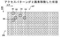
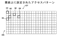
例えば、図19に示すように、水平方向に伸びる画素列が垂直方向に順次配列された画面SRNの上に5個の画素IM1〜IM5のパターンをアクセスパターンACPとして設定し、このアクセスパターンACPの設定位置を開始位置から画素列方向に移動していく場合を考える。この場合、画素列方向は水平方向であり、アクセスパターンACPの設定位置はラスタスキャン順に移動していく。また、図19の「□」は1画素を示しており、この図19におけるアクセスパターンACPの設定位置は、開始位置を示している。 For example, as shown in FIG. 19, a pattern of five pixels IM1 to IM5 is set as an access pattern ACP on a screen SRN in which pixel columns extending in the horizontal direction are sequentially arranged in the vertical direction. Consider a case where the set position is moved in the pixel column direction from the start position. In this case, the pixel column direction is the horizontal direction, and the setting position of the access pattern ACP moves in the raster scan order. Further, “□” in FIG. 19 indicates one pixel, and the setting position of the access pattern ACP in FIG. 19 indicates the start position.
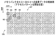
この画面SRNの各画素列の画素のデータを、左上の画素からラスタスキャン順に、図20に示すように、5個のメモリバンクBK0〜BK4に1画素ずつ順に格納したとする。図20の□内の数字はバンクアドレス0〜4を示している。この場合、アクセスパターンACPの設定位置が開始位置にあるとき、図21に示すように、アクセスパターンACPで特定される5個の画素IM1〜IM5の画素データは、メモリバンクBK0〜BK4の○印で示すアドレス位置に格納されていることから、5個の画素データに同時にアクセスして読み出すことができる。 It is assumed that the pixel data of each pixel column of the screen SRN is stored in order of raster scan from the upper left pixel, one pixel at a time in five memory banks BK0 to BK4 as shown in FIG. The numbers in the squares in FIG. 20 indicate the bank addresses 0-4. In this case, when the setting position of the access pattern ACP is at the start position, as shown in FIG. 21, the pixel data of the five pixels IM1 to IM5 specified by the access pattern ACP are marked with ○ in the memory banks BK0 to BK4. Since the pixel data is stored in the address position indicated by (5), five pixel data can be simultaneously accessed and read out.
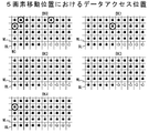
アクセスパターンACPの設定位置が開始位置から1画素ずつ移動して4画素の移動までは、上述した設定位置が開始位置にある場合と同様に、5個の画素データに同時にアクセスして読み出すことができる。しかし、図22に示すように、アクセスパターンACPの設定位置が5画素移動したとき、アクセスパターンACPで特定される5個の画素IM1〜IM5の画素データは、図23に示すように、メモリバンクBK0〜BK4の○印で示すアドレス位置に格納されており、メモリバンクBK0で複数のワード線のデータにアクセスすることが必要になるので、5個の画素データに同時アクセスして読み出すことができなくなる。 In the same manner as in the case where the set position is at the start position, the five pixel data can be simultaneously accessed and read out until the set position of the access pattern ACP moves one pixel at a time from the start position to four pixels. it can. However, as shown in FIG. 22, when the setting position of the access pattern ACP moves by 5 pixels, the pixel data of the five pixels IM1 to IM5 specified by the access pattern ACP are stored in the memory bank as shown in FIG. Since it is stored in the address positions indicated by ◯ in BK0 to BK4 and it is necessary to access data of a plurality of word lines in the memory bank BK0, it is possible to simultaneously access and read out five pixel data. Disappear.
アクセスパターンによっては、格納場所を上手く選べば同時にアクセスできるが、どのようなアクセスパターンでも複数の画素データに同時にアクセスできるようにするためには、1メモリバンクが1ワード線だけで構成されるぐらい細かく、バンク分割する必要がある。しかし、細かく分割するほどバンク数は多くなり、(a)それぞれのバンクに異なるアドレスを指定するのでアドレスバスが膨大になる、(b)デコーダやセレクタがバンクの数だけ必要なのでチップ面積が大きくなる、(c)同時に複数のバンクが動作するため消費電力が多くなる、等の問題点が出てくる。 Depending on the access pattern, it can be accessed at the same time if the storage location is selected well, but in order to be able to access a plurality of pixel data simultaneously in any access pattern, one memory bank is composed of only one word line. It is necessary to divide the bank finely. However, the smaller the number of banks, the larger the number of banks. (A) Since different addresses are designated for each bank, the address bus becomes enormous. (B) The chip area is increased because the number of decoders and selectors required is the same as the number of banks. (C) The problem arises that the power consumption increases because a plurality of banks operate simultaneously.
なお、アクセスパターンに対応した複数の画素データに時分割でアクセスし、キャッシュやバッファに一時記憶し、見かけ上の同時アクセスを達成することが提案されているが(実開昭63−35146号公報、実開平8−896号公報参照)、時間的な遅れが発生するという問題点があった。 It has been proposed that a plurality of pixel data corresponding to an access pattern is accessed in a time-sharing manner and temporarily stored in a cache or buffer to achieve apparent simultaneous access (Japanese Utility Model Publication No. 63-35146). And Japanese Utility Model Laid-Open No. 8-896), there is a problem that a time delay occurs.
この発明の目的は、アクセスパターンの設定位置を開始位置から画素列方向に移動した各設定位置で、当該アクセスパターンで特定される複数の画素の画素データを同時に取得することを容易に行い得るようにすることにある。 An object of the present invention is to easily obtain pixel data of a plurality of pixels specified by the access pattern at each setting position where the setting position of the access pattern is moved in the pixel column direction from the start position. Is to make it.
この発明の概念は、
複数のメモリバンクからなるメモリ部と、
水平または垂直の方向に伸びる画素列が垂直または水平の方向に順次配列された所定画面における各画素列の画素を順に注目画素とし、該注目画素の画素データを上記複数のメモリバンクに振り分けて格納するための制御を行うデータ格納制御部と、
上記所定画面上に設定される複数の画素のパターンをアクセスパターンとし、上記複数のメモリバンクから、上記アクセスパターンの設定位置を開始位置から画素列方向に移動した各設定位置で、上記アクセスパターンで特定される複数の画素の画素データを同時に取得するための制御を行うデータアクセス制御部とを備え、
上記データ格納制御部は、
上記設定位置の開始位置における上記アクセスパターンで特定される複数の画素に基づき、上記注目画素の画素データを最初のメモリバンクに格納することを開始した後、上記注目画素が上記複数の画素のいずれかになるとき、あるいは同一のメモリバンクに一定数の画素データを連続して格納したとき、上記注目画素の画素データを格納するメモリバンクを順次切り替え、
上記注目画素が上記複数の画素のいずれかになることで該注目画素の画素データを格納するメモリバンクを切り替えるとき、切り替え前のメモリバンクの書き込みアドレスを上記一定数に対応したアドレスの次のアドレスとし、
上記データアクセス制御部は、
上記設定位置が所定位置にあるとき、該所定位置における上記アクセスパターンで特定される複数の画素の画素データを上記複数のメモリバンクから同時に読み出し、上記設定位置が上記画素列方向に移動した際に、上記設定位置における上記アクセスパターンで特定される複数の画素の画素データがそれぞれ異なるメモリバンクに格納されているように、上記読み出した画素データのいずれかあるいは全部を、該画素データが格納されていたメモリバンクの1つ前のメモリバンクに格納する
ことを特徴とするデータアクセス装置にある。
The concept of this invention is
A memory unit composed of a plurality of memory banks;
Pixels in each pixel column in a predetermined screen in which pixel columns extending in the horizontal or vertical direction are sequentially arranged in the vertical or horizontal direction are used as target pixels in order, and the pixel data of the target pixel is distributed and stored in the plurality of memory banks. A data storage control unit for performing control to
A pattern of a plurality of pixels set on the predetermined screen is used as an access pattern, and from the plurality of memory banks, the setting position of the access pattern is moved in the pixel column direction from the start position, and the access pattern is A data access control unit that performs control to simultaneously acquire pixel data of a plurality of specified pixels,
The data storage control unit
Based on the plurality of pixels specified by the access pattern at the start position of the set position, after starting to store the pixel data of the target pixel in the first memory bank, the target pixel is one of the plurality of pixels. When a certain number of pixel data is stored continuously in the same memory bank, the memory banks for storing the pixel data of the pixel of interest are sequentially switched,
When switching the memory bank storing the pixel data of the pixel of interest by switching the pixel of interest to one of the plurality of pixels, the write address of the memory bank before switching is the next address after the address corresponding to the certain number age,
The data access control unit
When the set position is at a predetermined position, pixel data of a plurality of pixels specified by the access pattern at the predetermined position are simultaneously read from the plurality of memory banks, and the set position is moved in the pixel column direction. The pixel data is stored in any or all of the read pixel data so that the pixel data of the plurality of pixels specified by the access pattern at the set position are stored in different memory banks. In the data access device, the data is stored in a memory bank immediately preceding the memory bank.
この発明においては、水平または垂直の方向に伸びる画素列が垂直または水平の方向に順次配列された所定画面における各画素列の画素を順に注目画素とし、この注目画素の画素データを複数のメモリバンクに振り分けて格納する。 In the present invention, pixels of each pixel column in a predetermined screen in which pixel columns extending in the horizontal or vertical direction are sequentially arranged in the vertical or horizontal direction are sequentially used as the target pixel, and the pixel data of the target pixel is stored in a plurality of memory banks. Sort and store.
例えば、データ格納制御部は、注目画素が、開始位置に設定されたアクセスパターンで特定される複数の画素(初期アクセス画素)に一致する画素であるか否かを判定する一致判定部と、この一致判定部における一致判定出力でカウントを開始し、同一のメモリバンクに連続して格納される画素データの個数をカウントするカウント部と、一致判定部の判定出力およびカウント部のカウント値に基づいて、注目画素毎に、メモリ部に対する書き込みアドレスを生成するアドレス生成部とを有する。 For example, the data storage control unit includes a match determination unit that determines whether or not the target pixel is a pixel that matches a plurality of pixels (initial access pixels) specified by the access pattern set at the start position. Counting is started by the coincidence determination output in the coincidence determination unit, based on the count unit that counts the number of pixel data continuously stored in the same memory bank, the determination output of the coincidence determination unit, and the count value of the count unit And an address generation unit that generates a write address for the memory unit for each pixel of interest.
この場合、1番目の画素から順に注目画素となり、最初は複数のメモリバンクのうち最初のメモリバンクに格納される。その後、注目画素が複数の初期アクセス画素のいずれかになるとき、あるいは同一のメモリバンクに一定数の画素データを連続して格納したとき、注目画素の画素データを格納するメモリバンクが順次切り替えられる。 In this case, the pixel of interest is sequentially from the first pixel, and is initially stored in the first memory bank among the plurality of memory banks. After that, when the target pixel becomes one of a plurality of initial access pixels, or when a fixed number of pixel data is continuously stored in the same memory bank, the memory bank for storing the pixel data of the target pixel is sequentially switched. .
これにより、開始位置に設定されたアクセスパターンで特定される複数の初期アクセス画素の画素データはそれぞれ異なるメモリバンクに格納された状態となって同時アクセスが可能となり、また複数のメモリバンクに格納される画素データの数が平均化されるため、メモリバンクの容量を小さくできる。 As a result, the pixel data of a plurality of initial access pixels specified by the access pattern set at the start position are stored in different memory banks, and can be accessed simultaneously, and stored in a plurality of memory banks. Since the number of pixel data to be averaged is averaged, the capacity of the memory bank can be reduced.
またこの場合、注目画素が初期アクセス画素のいずれかとなることでこの注目画素の画素データを格納するメモリバンクを切り替えるとき、切り替え前のメモリバンクの書き込みアドレスが一定数に対応したアドレスの次のアドレスとされる。これにより、この切り替え前のメモリバンクに画素データが格納されていない領域が形成され、後述するように後のメモリバンクから読み出された画素データの格納が可能となる。 Further, in this case, when the memory pixel storing the pixel data of the target pixel is switched because the target pixel is one of the initial access pixels, the write address of the memory bank before switching is the next address after the address corresponding to a certain number. It is said. As a result, an area where no pixel data is stored is formed in the memory bank before switching, and pixel data read from the subsequent memory bank can be stored as will be described later.
また、この発明においては、アクセスパターンの設定位置が開始位置から画素列方向に移動した各設定位置で、アクセスパターンで特定される複数の画素(アクセス画素)の画素データを、複数のメモリバンクから同時に取得する。 In the present invention, the pixel data of a plurality of pixels (access pixels) specified by the access pattern is obtained from the plurality of memory banks at each setting position where the setting position of the access pattern is moved in the pixel column direction from the start position. Get at the same time.
例えば、データアクセス制御部は、複数のメモリバンクの読み出し開始アドレスを設定する読み出し開始アドレス設定部と、複数のメモリバンクの書き込み開始アドレスを設定する書き込み開始アドレス設定部と、複数のメモリバンクの読み出しアドレスを生成する読み出しアドレス生成部と、複数のメモリバンクの書き込みアドレスを生成する書き込みアドレス生成部と、複数のメモリバンクの、読み出しを行うか否かを示す読み出しフラグを生成する読み出しフラグ生成部と、複数のメモリバンクの、書き込みを行うか否かを示す書き込みフラグを生成する書き込みフラグ生成部と、最初に複数のアクセス画素のうち1番目の画素の画素データが格納されたメモリバンクを指定し、その後はアクセスパターンの設定位置が一定数だけ移動する毎に複数のメモリバンクを順次指定するバンク指定部とを有する。 For example, the data access control unit includes a read start address setting unit that sets read start addresses for a plurality of memory banks, a write start address setting unit that sets write start addresses for a plurality of memory banks, and a read operation for a plurality of memory banks. A read address generator for generating addresses, a write address generator for generating write addresses for a plurality of memory banks, a read flag generator for generating a read flag indicating whether or not to read a plurality of memory banks, and A write flag generation unit for generating a write flag indicating whether or not to perform writing in a plurality of memory banks, and a memory bank in which pixel data of a first pixel among a plurality of access pixels is first stored After that, the access pattern setting position moves by a certain number And a bank specifying unit that sequentially specifies a plurality of memory banks for each that.
そして、読み出し開始アドレス設定部は、各メモリバンクのそれぞれに対し、最初の読み出し開始アドレスを外部から与えられる読み出し開始アドレスとし、アクセスパターンの設定位置が一定数だけ移動する毎の読み出し開始アドレスを、バンク指定部で指定されていないメモリバンクについては1つ前のメモリバンクの書き込みフラグがフラグオフの状態となったときの読み出しアドレスとし、バンク指定部で指定されているメモリバンクについては1つ前のメモリバンクの書き込みフラグがフラグオフとなったときの読み出しアドレスを一定数だけ進めたアドレスとする。 Then, the read start address setting unit sets the first read start address as the read start address given from the outside for each of the memory banks, and sets the read start address every time the access pattern setting position moves by a certain number, For a memory bank that is not specified in the bank specification section, it is a read address when the write flag of the previous memory bank is in a flag-off state, and for a memory bank that is specified in the bank specification section, the previous one It is assumed that the read address when the write flag of the memory bank is turned off is an address advanced by a certain number.
また、書き込み開始アドレス設定部は、各メモリバンクのそれぞれに対し、最初の書き込み開始アドレスを、外部から与えられる書き込み開始アドレスとし、アクセスパターンの設定位置が一定数だけ移動する毎の書き込み開始アドレスを、バンク指定部で指定されていないメモリバンクについては直前の読み出し開始アドレスとし、バンク指定部で指定されているメモリバンクについては直前の読み出し開始アドレスを一定数だけ進めたアドレスを書き込み開始アドレスとする。 The write start address setting unit sets the first write start address for each memory bank as the write start address given from the outside, and sets the write start address every time the access pattern setting position moves by a certain number. A memory bank not designated by the bank designating unit is set as the immediately preceding read start address, and a memory bank designated by the bank designating unit is designated as an address obtained by advancing the previous read start address by a certain number. .
また、読み出しアドレス生成部は、各メモリバンクのそれぞれに対し、最初およびアクセスパターンの設定位置が一定数だけ移動する毎に、読み出し開始アドレス設定部で設定された読み出し開始アドレスを読み出しアドレスとし、各設定位置で画素データの読み出しが行われるとき、読み出しアドレスをインクリメントし、読み出し開始アドレスが一定数の(R−1)倍を越えると共にR倍以下にあるとき(Rは正の整数)、インクリメントされたアドレスが一定数のR倍を越えないときはこのインクリメントされたアドレスを次の読み出しアドレスとし、インクリメントされたアドレスが一定数のR倍を越えるときはこのインクリメントされたアドレスを一定数だけ戻したアドレスを次の読み出しアドレスとする。 Further, the read address generation unit uses the read start address set by the read start address setting unit as a read address every time the initial and access pattern setting positions move by a certain number for each memory bank, When pixel data is read out at the set position, the readout address is incremented, and when the readout start address exceeds a certain number (R-1) times and below R times (R is a positive integer), it is incremented. When the address does not exceed a certain number R times, the incremented address is set as the next read address, and when the incremented address exceeds a certain number R times, the incremented address is returned by a certain number. The address is set as the next read address.
また、書き込みアドレス生成部は、各メモリバンクのそれぞれに対し、最初およびアクセスパターンの設定位置が一定数だけ移動する毎に、書き込み開始アドレス設定部で設定された書き込み開始アドレスを書き込みアドレスとし、各設定位置で画素データの書き込みが行われるとき、書き込みアドレスをインクリメントし、書き込み開始アドレスが一定数の(R−1)倍を越えると共にR倍以下にあるとき(Rは正の整数)、インクリメントされたアドレスが一定数のR倍を越えないときはこのインクリメントされたアドレスを次の書き込みアドレスとし、インクリメントされたアドレスが一定数のR倍を越えるときはこのインクリメントされたアドレスを一定数だけ戻したアドレスを次の書き込みアドレスとする。 Further, the write address generation unit uses the write start address set by the write start address setting unit as the write address each time the initial and access pattern setting positions move by a certain number for each of the memory banks. When pixel data is written at the set position, the write address is incremented, and when the write start address exceeds a certain number (R-1) times and is less than R times (R is a positive integer), it is incremented. When the address does not exceed a certain number of R times, the incremented address is set as the next write address, and when the incremented address exceeds a certain number of R times, the incremented address is returned by a certain number. The address is set as the next write address.
また、読み出しフラグ生成部は、各メモリバンクのそれぞれに対し、最初は、外部から与えられる読み出しフラグに基づき、開始位置に設定されたアクセスパターンで特定される複数の画素(初期アクセス画素)の画素データのいずれかが格納されているメモリバンクについての読み出しフラグを読み出しを行うことを示すフラグオンの状態とし、その他のメモリバンクについての読み出しフラグを読み出しを行わないことを示すフラグオフの状態とし、アクセスパターンの設定位置が一定数だけ移動する毎に、1つ前のメモリバンクの読み出しフラグを新たな読み出しフラグとする。 In addition, the read flag generation unit first, for each of the memory banks, a plurality of pixels (initial access pixels) specified by an access pattern set at a start position based on a read flag given from outside. The read flag for the memory bank in which any of the data is stored is set to a flag-on state indicating that reading is performed, and the read flag for the other memory bank is set to a flag-off state indicating that reading is not performed, and the access pattern Each time the set position moves by a certain number, the read flag of the previous memory bank is set as a new read flag.
また、書き込みフラグ生成部は、各メモリバンクのそれぞれに対し、最初およびアクセスパターンの設定位置が一定数だけ移動する毎に、読み出し開始アドレス設定部で設定される読み出し開始アドレスと書き込み開始アドレス設定部で設定される書き込み開始アドレスに基づき、読み出し開始アドレスと書き込み開始アドレスが同じであるメモリバンクについての書き込みフラグを書き込みを行わないことを示すフラグオフの状態とし、その他のメモリバンクについての書き込みフラグを書き込みを行うことを示すフラグオンの状態とし、各設定位置毎に、書き込みアドレス生成部で生成された次の書き込みアドレスが読み出し開始アドレス生成部で生成された読み出し開始アドレスと同じになるメモリバンクについての書き込みフラグをフラグオンの状態からフラグオフの状態とする。
In addition, the write flag generation unit is configured so that the read start address and the write start address setting unit set by the read start address setting unit each time the initial and access pattern setting positions move by a certain number for each memory bank. Based on the write start address set in
この場合、アクセスパターンの設定位置が所定位置にあるとき、この所定位置におけるアクセスパターンで特定される複数の画素(アクセス画素)の画素データが複数のメモリバンクから同時に読み出されると共に、この設定位置が画素列方向に移動した際に、設定位置におけるアクセスパターンで特定される複数の画素の画素データがそれぞれ異なるメモリバンクに格納されているように、読み出された画素データのいずれかあるいは全部が、その画素データが格納されていたメモリバンクの1つ前のメモリバンクに格納される。これにより、アクセスパターンの設定位置が開始位置から移動した全ての位置で、当該アクセスパターンで特定される複数のアクセス画素の画素データがそれぞれ異なるメモリバンクに格納された状態となって同時アクセスが可能となる。 In this case, when the setting position of the access pattern is at a predetermined position, the pixel data of the plurality of pixels (access pixels) specified by the access pattern at the predetermined position are simultaneously read from the plurality of memory banks, and the setting position is When moving in the pixel column direction, any or all of the read pixel data is stored such that the pixel data of the plurality of pixels specified by the access pattern at the set position is stored in different memory banks, The pixel data is stored in the memory bank immediately preceding the memory bank in which the pixel data was stored. As a result, at all positions where the access pattern setting position has moved from the start position, the pixel data of a plurality of access pixels specified by the access pattern are stored in different memory banks, allowing simultaneous access. It becomes.
例えば、データアクセス制御部に与えられる読み出しフラグは、データ格納制御部から与えられる。この場合、データ格納制御部は、複数のメモリバンクのそれぞれに対応した、読み出しを行うか否かを示す読み出しフラグを生成する読み出しフラグ生成部をさらに有し、この読み出しフラグ生成部は、複数の画素のいずれかに対応する画素データが格納されるメモリバンクに対する読み出しフラグを読み出しを行うことを示すフラグオンの状態とし、その他のメモリバンクに対する読み出しフラグを読み出しを行わないことを示すフラグオフの状態とする。このように、データ格納制御部からデータアクセス制御部に読み出しフラグを与えることで、例えばこれらデータ格納制御部およびデータアクセス制御部を制御する制御装置が、アクセスパターンおよび一定数の情報に基づいて読み出しフラグを生成して、データアクセス制御部に与えることが必要でなくなる。 For example, the read flag given to the data access control unit is given from the data storage control unit. In this case, the data storage control unit further includes a read flag generation unit that generates a read flag indicating whether or not to perform reading corresponding to each of the plurality of memory banks. A read flag for a memory bank in which pixel data corresponding to one of the pixels is stored is turned on, and a read flag for another memory bank is turned off to indicate that no read is performed. . In this way, by giving a read flag to the data access control unit from the data storage control unit, for example, the control device that controls the data storage control unit and the data access control unit reads based on the access pattern and a certain number of information. It is not necessary to generate a flag and give it to the data access control unit.
また例えば、データアクセス制御部に与えられる読み出し開始アドレスおよび書き込み開始アドレスは、データ格納制御部から与えられる。この場合、データ格納制御部は、複数のメモリバンクのそれぞれに対応した、読み出し開始アドレスおよび書き込み開始アドレスを生成する開始アドレス生成部をさらに有し、この開始アドレス生成部は、それぞれのメモリバンクに対して、複数のアクセス画素の1番目の画素以降の画素のデータであって最初の画素データが格納されたアドレスを読み出し開始アドレスとし、最初の画素データから連続して格納された画素データの個数が一定数であるとき読み出し開始アドレスを書き込み開始アドレスとし、最初の画素データから連続して格納された画素データの個数が一定数に満たないとき、最後の画素データが格納されたアドレスの次のアドレスを書き込み開始アドレスとする。このように、データ格納制御部からデータアクセス制御部に読み出し開始アドレスおよび書き込み開始アドレスを与えることで、例えばこれらデータ格納制御部およびデータアクセス制御部を制御する制御装置が、アクセスパターンおよび一定数の情報に基づいて読み出し開始アドレスおよび書き込み開始アドレスを生成して、データアクセス制御部に与えることが必要でなくなる。 Further, for example, the read start address and the write start address given to the data access control unit are given from the data storage control unit. In this case, the data storage control unit further includes a start address generation unit that generates a read start address and a write start address corresponding to each of the plurality of memory banks, and the start address generation unit is provided in each memory bank. On the other hand, the number of pixel data stored successively from the first pixel data, with the address of the first and subsequent pixels of the plurality of access pixels as the read start address being the address where the first pixel data is stored When the number of pixel data continuously stored from the first pixel data is less than a certain number, the next address after the address where the last pixel data is stored The address is set as the write start address. In this way, by giving the read start address and the write start address from the data storage control unit to the data access control unit, for example, the control device that controls the data storage control unit and the data access control unit has an access pattern and a certain number of It is not necessary to generate a read start address and a write start address based on the information and give them to the data access control unit.
この発明によれば、アクセスパターンの設定位置を開始位置から画素列方向に順次移動した各設定位置で、当該アクセスパターンで特定される複数の画素の画素データがそれぞれ異なるメモリバンクに格納された状態として、当該複数の画素データを同時にアクセスできるようにしたものであり、当該複数の画素データの同時取得を容易に行うことができる。 According to the present invention, pixel data of a plurality of pixels specified by the access pattern is stored in different memory banks at each setting position where the setting position of the access pattern is sequentially moved from the start position in the pixel column direction. The plurality of pieces of pixel data can be accessed simultaneously, and the plurality of pieces of pixel data can be easily acquired simultaneously.
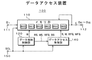
以下、図面を参照しながら、この発明の実施の形態について説明する。図1は、実施の形態としてのデータアクセス装置100の構成を示している。
Hereinafter, embodiments of the present invention will be described with reference to the drawings. FIG. 1 shows a configuration of a
このデータアクセス装置100は、メモリ部110と、データ格納制御部120と、データアクセス制御部140とを備えている。
The
メモリ部110は、6個のメモリバンクBK0〜BK5からなっている。このメモリ部110は、図示しない制御装置から入力端子150を介して与えられる制御信号SCLに基づいて動作する。
The
このメモリ部110には、初期格納時に、入力端子111から、格納すべき所定画面の画素データDiが入力される。ここで、所定画面は、水平方向に伸びる画素列が垂直方向に順次配列された構成となっており、メモリ部110には各画素列の画素データが順に注目画素としてラスタスキャン順に入力されていく。そして、このようにメモリ部110に入力されていく各注目画素の画素データは6個のメモリバンクBK0〜BK5に振り分けて格納される。
The
また、データアクセス時に、画面上に複数の画素のパターンがアクセスパターンACPとして設定され、このアクセスパターンACPの設定位置が開始位置から画素列方向に1画素ずつ移動した各設定位置で、アクセスパターンACPで特定される複数の画素(以下、適宜、「アクセス画素」という)の画素データDo1〜Do5が、6個のメモリバンクBK0〜BK5のいずれかから同時に読み出されて、出力端子112に出力される。
During data access, a pattern of a plurality of pixels is set as an access pattern ACP on the screen, and the access pattern ACP is set at each setting position where the setting position of the access pattern ACP is moved by one pixel from the start position in the pixel column direction. Pixel data Do1 to Do5 of a plurality of pixels (hereinafter referred to as “access pixels” where appropriate) are simultaneously read from any of the six memory banks BK0 to BK5 and output to the
この場合、アクセスパターンACPの設定位置は、ラスタスキャン順に移動していく。この実施の形態では、アクセスパターンACPは5個の画素のパターンとされ、上述の各設定位置でアクセスパターンACPで特定される5個のアクセス画素の画素データDo1〜Do5が同時に読み出される。なお、このように各設定位置で読み出される画素データDo1〜Do5は、他のメモリバンクに格納すべき画素データとして、メモリ部110に再入力される。
In this case, the setting position of the access pattern ACP moves in the raster scan order. In this embodiment, the access pattern ACP is a pattern of five pixels, and the pixel data Do1 to Do5 of the five access pixels specified by the access pattern ACP are read simultaneously at each of the above-described setting positions. Note that the pixel data Do1 to Do5 read at each setting position in this way are re-input to the
データ格納制御部120は、図示しない制御装置から入力端子150を介して供給される制御信号SCLに基づいて動作する。このデータ格納制御部120は、上述したように、各注目画素の画素データをメモリ部110の6個のメモリバンクBK0〜BK5に振り分けて格納するための制御を行う。つまり、このデータ格納制御部120は、1番目の画素から順に注目画素とし、最初は6個のメモリバンクBK0〜BK5のうち最初のメモリバンク、つまりメモリバンクBK0にその注目画素の画素データを格納する。
The data
その後に、このデータ格納制御部120は、開始位置に設定されたアクセスパターンACPで特定される5個の画素(以下、適宜、「初期アクセス画素」という)IM1〜IM5に基づき、注目画素が5個の初期アクセス画素IM1〜IM5のいずれかとなるとき、あるいは同一のメモリバンクに一定数Nの画素データを連続して格納したとき、注目画素の画素データを格納するメモリバンクを順次切り替える。この実施の形態では、画面の水平方向に伸びる画素列の画素数が22個とされ、一定数Nは画素列の画素数と同じく22とされている。
After that, the data
また、このデータ格納制御部120は、注目画素が5個の初期アクセス画素IM1〜IM5のいずれかになることでメモリバンクを切り替えるとき、切り替え前のメモリバンクの書き込みアドレスを一定数だけ進めて次の書き込みアドレスとする。
In addition, when the memory bank is switched because the target pixel is any of the five initial access pixels IM1 to IM5, the data
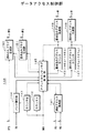
データ格納制御部120についてさらに詳細に説明する。図2は、このデータ格納制御部120の構成を示している。このデータ格納制御部120は、カウンタ(カウンタA)121と、カウンタ(カウンタB)122と、一致判定部123と、オフセット制御部124と、バンクアドレスカウンタ125と、ビット線アドレスカウンタ126と、ワード線アドレスカウンタ127と、アドレス生成部128と、読み出しフラグ生成部129とを有している。
The data
カウンタ(カウンタA)121は、上述したメモリ部111に順に入力される各注目画素の画素データの入力個数をカウントする。このカウンタ121には、メモリ部110に入力される各注目画素の画素データに同期したデータクロックDCKが供給される。このデータクロックDCKは、上述した制御信号SCLのひとつを構成しており、図示しない制御装置から供給される。このカウンタ121は、最初にそのカウント値が0とされ、その後はメモリ部110に各注目画素の画素データが入力される毎に、データクロックDCKによってインクリメントされていく。
The counter (counter A) 121 counts the number of input pixel data of each pixel of interest that is sequentially input to the
一致判定部123は、上述したメモリ部110に所定の注目画素の画素データが入力される毎に、その注目画素が、開始位置に設定されたアクセスパターンACPで特定される5個の初期アクセス画素に一致するか否かを判定する。そのため、この一致判定部123には、注目画素が当該5個の初期アクセス画素となるときに上述したカウンタ121から出力されるカウント値CN1〜CN5が、アクセスパターン情報IAPとして供給される。このアクセスパターン情報IAPは、上述した制御信号SCLのひとつを構成しており、図示しない制御装置から供給される。この一致判定部123は、ある注目画素におけるカウンタ121のカウント値が、カウント値CN1〜CN5と一致するとき、それぞれ、当該注目画素は1番目〜5番目の初期アクセス画素であると判定する。
Each time the pixel data of a predetermined target pixel is input to the
カウンタ(カウンタB)122は、同一のメモリバンクに連続して格納される画素データの個数をカウントする。このカウンタ122には、メモリ部110に入力される各注目画素の画素データに同期したデータクロックDCKが供給されると共に、上述した一致判定部123の判定出力が供給される。このカウンタ122は、最初はそのカウント値が0とされ、上述した一致判定部123で注目画素が初期アクセス画素であると判定されるか、同一のメモリバンクに連続して格納される画素データの個数が一定数Nとなり、カウント値が一定数Nを越えるとき、そのカウント値が1にセットされ、その後はメモリ部110に各注目画素の画素データが入力される毎に、データクロックDCKによってインクリメントされていく。
The counter (counter B) 122 counts the number of pixel data stored continuously in the same memory bank. The
バンクアドレスカウンタ125は、6個のメモリバンクBK0〜BK5のうち注目画素の画素データを格納すべきメモリバンクを示すカウント値、つまりバンクアドレスを出力する。このバンクアドレスカウンタ125には、上述した一致判定部123の判定出力が供給されると共に、カウンタ122のカウント値が供給される。このバンクアドレスカウンタ125は、最初はそのカウント値が0とされ、その後に注目画素が初期アクセス画素のいずれかであると判定されるか、あるいは同一メモリバンクに連続して格納される画素データの個数が一定数Nとなり、カウンタ122のカウント値が一定数Nを越えるとき、インクリメントされる。このバンクアドレスカウンタ125は、カウント値5の次はカウント値0となり、6進カウンタの構成となっている。このバンクアドレスカウンタ125のカウント値0〜5、つまりバンクアドレス0〜5は、それぞれメモリバンクBK0〜BK5を示している。
The
ビット線アドレスカウンタ126は、6個のメモリバンクBK0〜BK5にそれぞれ対応した6個のカウンタ126-0〜126-5からなっている。このビット線アドレスカウンタ126には、メモリ部110に入力される各注目画素の画素データに同期したデータクロックDCKが供給されると共に、バンクアドレスカウンタ125のカウント値(バンクアドレス)が供給される。これらのカウンタ126-0〜126-5は、最初はそのカウント値、つまりビット線アドレスが0とされ、その後はメモリ部110に各注目画素の画素データが入力されて格納される毎に、カウンタ126-0〜126-5のうちバンクアドレスに対応したカウンタがインクリメントされていく。この実施の形態では、各メモリバンクBK0〜BK5のワード線長は10とされ、カウンタ126-0〜126-5は、カウント値9の次はカウント値0となり、10進カウンタの構成となっている。
The bit
ワード線アドレスカウンタ127は、6個のメモリバンクBK0〜BK5にそれぞれ対応した6個のカウンタ127-0〜127-5からなっている。これらのカウンタ127-0〜127-5には、それぞれ上述したカウンタ126-0〜126-5の桁上げ信号であるキャリーCAが供給される。これらのカウンタ127-0〜127-5は、それぞれ、カウンタ126-0〜126-5からキャリーCAが供給される毎に、インクリメントされていく。
The word
オフセット制御部124は、ビット線アドレスカウンタ126およびワード線アドレスカウンタ127のカウント値のオフセット制御をする。このオフセット制御部124には、一致判定部123の判定出力が供給されると共に、バンクアドレスカウンタ125のカウント値(バンクアドレス)が供給される。このオフセット制御部124は、注目画素が初期アクセス画素のいずれかとなるとき、バンクアドレスカウンタ125のカウント値で示されるメモリバンクの書き込みアドレスが一定数Nに対応したアドレスの次のアドレスとなるように、ビット線アドレスカウンタ126およびワード線アドレスカウンタ127にオフセットを与える。
The offset
アドレス生成部128は、メモリ部110に供給する書き込みアドレスWを生成する。このアドレス生成部128には、カウンタ125〜127のカウント値が供給されると共に、カウンタ122のカウント値が供給される。このアドレス生成部128は、バンクアドレスカウンタ125のカウント値(バンクアドレス)、ビット線アドレスカウンタ126を構成するカウンタ126-0〜126-5のうちバンクアドレスに対応したカウンタのカウント値(ビット線アドレス)、およびワード線アドレスカウンタ127を構成するカウンタ127-0〜127-5のうちバンクアドレスに対応したカウンタのカウント値(ワード線アドレス)を合成して、メモリ部110に供給する書き込みアドレスWを生成する。
The
また、このアドレス生成部128は、データアクセス制御部140で用いられる、それぞれのメモリバンクBK0〜BK5に対する、読み出し開始アドレスRSおよび書き込み開始アドレスWSを生成する。この場合、アドレス生成部128は、それぞれのメモリバンクBK0〜BK5の、初期アクセス画素の1番目の画素以降のデータであって最初に画素データが格納された書き込みアドレスWを読み出し開始アドレスRSとする。また、アドレス生成部128は、最初の画素データから連続して格納された画素データの個数が一定数Nであるとき読み出し開始アドレスRSを書き込み開始アドレスWSとし、最初の画素データから連続して格納された画素データの個数が一定数Nに満たないとき、最後の画素データが格納されたアドレスの次のアドレスを書き込み開始アドレスWSとする。
The
また、アドレス生成部128は、データアクセス制御部140のバンク指定部のカウンタの初期値BSを生成する。この場合、5個の初期アクセス画素のうち1番目の初期アクセス画素の画素データが格納されたメモリバンクを示すバンクアドレス(バンクアドレスカウンタ125のカウント値)を初期値とする。
Further, the
読み出しフラグ生成部129は、データアクセス制御部140で用いられる、それぞれのメモリバンクBK0〜BK5に対する読み出しフラグRFGを生成する。この読み出しフラグ生成部129には、一致判定部123の判定出力が供給されると共に、バンクアドレスカウンタ125のカウント値(バンクアドレス)が供給される。この読み出しフラグ生成部129は、6個のメモリバンクBK0〜BK5のうち、5個の初期アクセス画素のいずれかに対応する画素データが格納されるメモリバンクに対する読み出しフラグRFGを読み出しを行うことを示すフラグオンの状態、例えば1とし、その他のメモリバンクに対する読み出しフラグRFGを読み出しを行わないことを示すフラグオフの状態、例えば0とする。
The read
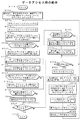
次に、図2に示すデータ格納制御部120の制御による初期格納時の動作を、図3のフローチャートを用いて説明する。なお、データ格納制御部120は、例えばマイクロプロセッサで構成され、図示しないプログラムメモリに格納されたデータ格納制御プログラムに従って制御処理をする。
Next, the operation at the time of initial storage under the control of the data
ステップST1で、動作を開始し、ステップST2で、バンクアドレスカウンタ125のカウント値(バンクアドレス)、ビット線アドレスカウンタ126(カウンタ126-0〜126-5)のカウント値(ビット線アドレス)およびワード線アドレスカウンタ127(カウンタ127-0〜127-5)のカウント値(ワード線アドレス)をそれぞれ0にし、カウンタ(カウンタA)121およびカウンタ(カウンタB)122のカウント値をそれぞれ0にし、さらに読み出しフラグ生成部129から出力される各メモリバンクBK0〜BK5に対応する読み出しフラグRFGを全て読み出しを行わないことを示すフラグオフの状態、例えば0にする。
In step ST1, and starts operating, in step ST2, the count value (bank address) of the
次に、ステップST3で、注目画素の画素データが入力されたか否かを判定する。この場合、データクロックDCKが供給されるとき、注目画素の画素データが入力されたと判定する。注目画素の画素データが入力されたと判定するとき、ステップST4で、カウンタ(カウンタA)121をインクリメントする。そして、ステップST5で、注目画素が初期アクセス画素であるか否かを、一致判定部123で判定する。この場合、カウンタ(カウンタA)121のカウント値が、アクセスパターン情報IAPとしてのカウント値CN1〜CN5のいずれかと一致するとき、注目画素が初期アクセス画素であると判定する。
Next, in step ST3, it is determined whether pixel data of the target pixel has been input. In this case, when the data clock DCK is supplied, it is determined that the pixel data of the target pixel has been input. When it is determined that pixel data of the target pixel has been input, the counter (counter A) 121 is incremented in step ST4. In step ST5, the
注目画素が初期アクセス画素であると判定するとき、ステップST6で、注目画素が1番目の画素であるか否か、すなわちカウンタ(カウンタA)121のカウント値が1であるか否かを判定する。注目画素が1番目の画素でないときは、ステップST7で、注目画素が1番目の初期アクセス画素であるか否かを、一致判定部123で判定する。この場合、カウンタ(カウンタA)121のカウント値が、アクセスパターン情報IAPとしてのカウント値CN1と一致するとき、注目画素が1番目の初期アクセス画素であると判定する。
When it is determined that the target pixel is the initial access pixel, it is determined in step ST6 whether or not the target pixel is the first pixel, that is, whether or not the count value of the counter (counter A) 121 is 1. . If the target pixel is not the first pixel, the
注目画素が1番目の初期アクセス画素ではなく、2番目以降の初期アクセス画素であると判定するとき、ステップST8で、書き込みアドレスWを、バンクアドレスに対応したメモリバンクの書き込み開始アドレスWSにし、その後にステップST9に進む。この書き込みアドレスWは、アドレス生成部128で、バンクアドレスカウンタ125のカウント値(バンクアドレス)、ビット線アドレスカウンタ126のバンクアドレスに対応したカウンタのカウント値(ビット線アドレス)およびワード線アドレスカウンタ127のバンクアドレスに対応したカウンタのカウント値(ワード線アドレス)を合成することで生成されている。
When it is determined that the target pixel is not the first initial access pixel but the second and subsequent initial access pixels, in step ST8, the write address W is set to the write start address WS of the memory bank corresponding to the bank address, and thereafter Then, the process proceeds to step ST9. This write address W is stored in the
一方、注目画素が1番目の初期アクセス画素であるときは、直ちにステップST9に進む。このステップST9では、オフセット制御部124は、バンクアドレスに対応したメモリバンクの書き込みアドレスWが一定数N、この実施の形態では22に対応したアドレスの次のアドレスとなるように、ビット線アドレスカウンタ126の当該バンクアドレスに対応したカウンタおよびワード線アドレスカウンタ127の当該バンクアドレスに対応したカウンタにオフセットを与える。そして、ステップST10で、バンクアドレスカウンタ125のカウント値(バンクアドレス)をインクリメントする。その後に、ステップST11に進む。
On the other hand, when the target pixel is the first initial access pixel, the process immediately proceeds to step ST9. In this step ST9, the offset
ステップST6で、注目画素が1番目の画素であるときは、直ちにステップST11に進む。このステップST11では、注目画素が1番目の初期アクセス画素であるか否かを、一致判定部123で判定する。注目画素が1番目の初期アクセス画素であるときは、ステップST12で、バンクアドレスカウンタ125のカウント値(バンクアドレス)を、データアクセス制御部140におけるバンク指定部のカウンタの初期値にする。その後にステップST13に進む。一方、注目画素が1番目の初期アクセス画素でないときは、直ちに、ステップST13に進む。
If the target pixel is the first pixel in step ST6, the process immediately proceeds to step ST11. In step ST11, the
ステップST13では、読み出しフラグ生成部129は、バンクアドレスに対応したメモリバンクの読み出しフラグRFGを読み出しを行うことを示すフラグオンの状態、例えば1にする。そして、ステップST14で、アドレス生成部128で生成されている書き込みアドレスWを、バンクアドレスに対応したメモリバンクの読み出し開始アドレスRSにする。その後に、ステップST15に進む。
In step ST13, the read
ステップST15では、インクリメントされたバンクアドレスに対応した、すなわち切り替えられたメモリバンクへの画素データの連続した格納個数をカウントするために、カウンタ(カウンタB)122を1にセットする。そして、ステップST16で、アドレス生成部128で生成されている書き込みアドレスWに基づき、当該書き込みアドレスWのバンクアドレスで指定されるメモリバンクの、当該書き込みアドレスWのビット線アドレスおよびワード線アドレスで指定されるアドレス位置に、注目画素の画素データを格納する。
In step ST15, the counter (counter B) 122 is set to 1 in order to count the number of consecutive pixel data stored in the memory bank corresponding to the incremented bank address. In step ST16, based on the write address W generated by the
次に、ステップST17で、ビット線アドレスカウンタ126のバンクアドレスに対応したカウンタのカウント値(ビット線アドレス)をインクリメントする。そして、ステップST18で、ステップST17で、カウンタのカウント値が0となったとき、そのカウンタから出力されるキャリーCAにより、ワード線アドレスカウンタ127のバンクアドレスに対応したカウンタのカウント値(ワード線アドレス)をインクリメントする。その後に、ステップST19に進む。
Next, in step ST17, the count value (bit line address) of the counter corresponding to the bank address of the bit
このステップST19では、画面SRNの全ての画素の画素データが入力されたか否かを判定する。この場合、カウンタ(カウンタA)121のカウント値が、画面SRNを構成する画素の個数に等しいとき、全ての画素の画素データが入力されたと判定する。全ての画素の画素データが入力されたと判定するとき、ステップST20で、動作を終了する。一方、全ての画素の画素データが入力されていないと判定するとき、ステップST3に戻り、次の注目画素の画素データの入力を待つ。 In this step ST19, it is determined whether or not the pixel data of all the pixels on the screen SRN has been input. In this case, when the count value of the counter (counter A) 121 is equal to the number of pixels constituting the screen SRN, it is determined that the pixel data of all the pixels has been input. When it is determined that the pixel data of all the pixels has been input, the operation ends in step ST20. On the other hand, when it is determined that the pixel data of all the pixels has not been input, the process returns to step ST3 and waits for the input of the pixel data of the next pixel of interest.
また、上述のステップST5で、注目画素が初期アクセス画素ではないと判定するとき、ステップST21で、カウンタ(カウンタB)122のカウント値をインクリメントする。そして、ステップST22で、カウンタ(カウンタB)122のカウント値が一定数Nより大きいか否かを判定する。カウント値が一定数Nより大きいときは、ステップST23に進み、注目画素が1番目の初期アクセス画素の後の画素であるか否かを判定する。この場合、カウンタ(カウンタA)121のカウント値が、アクセスパターン情報IAPとしてのカウント値CN1より大きいとき、注目画素が1番目の初期アクセス画素の後の画素である判定する。 When it is determined in step ST5 that the target pixel is not the initial access pixel, the count value of the counter (counter B) 122 is incremented in step ST21. In step ST22, it is determined whether or not the count value of the counter (counter B) 122 is greater than a certain number N. When the count value is larger than the certain number N, the process proceeds to step ST23, where it is determined whether or not the target pixel is a pixel after the first initial access pixel. In this case, when the count value of the counter (counter A) 121 is larger than the count value CN1 as the access pattern information IAP, it is determined that the target pixel is a pixel after the first initial access pixel.
注目画素が1番目の初期アクセス画素の後の画素であるときは、ステップST24で、アドレス生成部128で、バンクアドレスに対応したメモリバンクの書き込み開始アドレスが既に設定されているか否かを判定する。設定されていないと判定するときは、ステップST25で、書き込み開始アドレスを、読み出し開始アドレスと同じアドレスにする。その後、ステップST26に進む。上述のステップST24で、既に設定されていると判定するときは、直ちにステップST26に進む。
When the target pixel is a pixel after the first initial access pixel, in step ST24, the
このステップST26では、バンクアドレスカウンタ125のカウント値(バンクアドレス)をインクリメントする。そして、ステップST27で、アドレス生成部128で、バンクアドレスに対応した読み出し開始アドレスが既に設定されているか否かを判定する。設定されていないと判定するときは、上述したステップST14に進み、アドレス生成部128で生成されている書き込みアドレスWを読み出し開始アドレスRSにする。一方、設定されていると判定するときは、上述したステップST15に進む。
In step ST26, the count value (bank address) of the
なお、上述のステップST23で、注目画素が1番目の初期アクセス画素の後でないときは、直ちに、ステップST15に進む。また、上述ステップST22で、カウンタ(カウンタB)122のカウント値が一定数Nより大きくないと判定するときは、注目画素の画素データを格納すべきメモリバンクの切り替えが必要ないので、直ちに上述したステップST16に進む。 If the target pixel is not after the first initial access pixel in step ST23 described above, the process immediately proceeds to step ST15. Further, when it is determined in step ST22 that the count value of the counter (counter B) 122 is not larger than the predetermined number N, it is not necessary to switch the memory bank in which the pixel data of the target pixel is stored. Proceed to step ST16.
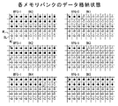
上述した初期格納時の動作により、画面SRNの各画素のデータは、図4、図5に示すように、メモリバンクBK0〜BK5に、振り分けられて格納される。 By the operation at the time of initial storage described above, the data of each pixel of the screen SRN is distributed and stored in the memory banks BK0 to BK5 as shown in FIGS.
図4の「□」は上述したように1画素を示しており、その□内の数字は、その画素の画素データが格納されるメモリバンクのバンクアドレスを示している。ここで、メモリバンクBK0〜BK5のバンクアドレスは、それぞれ、0〜5である。 “□” in FIG. 4 indicates one pixel as described above, and the number in the □ indicates the bank address of the memory bank in which the pixel data of the pixel is stored. Here, the bank addresses of the memory banks BK0 to BK5 are 0 to 5, respectively.
例えば、上述したように、画面SRNは水平方向に伸びる画素列が垂直方向に順次配列されたものであって、アクセスパターンACPは5個の画素IM1〜IM5のパターンからなっており、図4に示すアクセスパターンACPの設定位置がその開始位置であるとする。 For example, as described above, the screen SRN has pixel rows extending in the horizontal direction sequentially arranged in the vertical direction, and the access pattern ACP includes a pattern of five pixels IM1 to IM5. It is assumed that the set position of the access pattern ACP shown is the start position.
まず、第1列の先頭画素が注目画素となるが、この画素は1番目の初期アクセス画素IM1であり、この画素からメモリバンクBK0への画素データの格納が開始される。この場合、バンクアドレスカウンタ125のカウント値(バンクアドレス)が0にあるが、これがバンク指定部のカウンタの初期値とされる。またこの場合、このメモリバンクBK0の読み出しフラグRFGは読み出しを行うことを示すフラグオンの状態、例えば1に変更されると共に、この初期アクセス画素IM1の画素データを格納すべきアドレス位置を示すアドレス(書き込みアドレスW)が、当該メモリバンクBK0の読み出し開始アドレスRSとされる(図5のメモリバンクBK0参照)。
First, the first pixel in the first column is the target pixel. This pixel is the first initial access pixel IM1, and storage of pixel data from this pixel to the memory bank BK0 is started. In this case, the count value (bank address) of the
その後、この第1列の先頭画素に続く画素が順に注目画素となり、その画素データがメモリバンクBK0に格納されていく。このメモリバンクBK0に連続して22個(一定数N)だけ画素データが格納されるまでに、注目画素が2番目の初期アクセス画素IM2とならないので、当該メモリバンクBK0には22画素の画素データが連続して格納される(図5のメモリバンクBK0の最初の22個のアドレス位置参照)。 Thereafter, the pixel following the first pixel in the first column becomes the target pixel in order, and the pixel data is stored in the memory bank BK0. Since the pixel of interest does not become the second initial access pixel IM2 until 22 pixel data (a certain number N) are continuously stored in the memory bank BK0, the pixel data of 22 pixels is stored in the memory bank BK0. Are successively stored (see the first 22 address positions of the memory bank BK0 in FIG. 5).
そのため、このメモリバンクBK0の書き込み開始アドレスWSは、上述した読み出し開始アドレスRSと同じアドレスとされる(図5のメモリバンクBK0参照)。また、このメモリバンクBK0の次の書き込みアドレスWは、22個目の画素データが格納されたアドレス位置の次のアドレス位置を示すものとされる。 Therefore, the write start address WS of the memory bank BK0 is the same as the read start address RS described above (see the memory bank BK0 in FIG. 5). The next write address W of the memory bank BK0 indicates the next address position after the address position where the 22nd pixel data is stored.
メモリバンクBK0に22画素の画素データが連続して格納された後、バンクアドレスがインクリメントされて、画素データを格納すべきメモリバンクはBK1となる。この場合、第2列の先頭画素が注目画素となっており、この画素からメモリバンクBK1への画素データの格納が開始される。そして、この第2列の先頭画素の画素データを格納すべきアドレス位置を示すアドレス(書き込みアドレスW)が、当該メモリバンクBK1の読み出し開始アドレスRSとされる(図5のメモリバンクBK1参照)。 After the 22-pixel pixel data is continuously stored in the memory bank BK0, the bank address is incremented, and the memory bank to store the pixel data becomes BK1. In this case, the first pixel in the second column is the target pixel, and storage of pixel data from this pixel to the memory bank BK1 is started. The address (write address W) indicating the address position where the pixel data of the first pixel in the second column is to be stored is set as the read start address RS of the memory bank BK1 (see the memory bank BK1 in FIG. 5).
その後、第2列の先頭画素に続く画素が順に注目画素となって、その画素データがメモリバンクBK1に格納されていくが、第2列の4番目の画素は2番目の初期アクセス画素IM2であるので、この画素IM2が注目画素となるとき、バンクアドレスがインクリメントされて、画素データを格納すべきメモリバンクはBK2となる。 Thereafter, the pixel following the first pixel in the second column becomes the target pixel in order, and the pixel data is stored in the memory bank BK1, but the fourth pixel in the second column is the second initial access pixel IM2. Therefore, when this pixel IM2 becomes the target pixel, the bank address is incremented, and the memory bank to store the pixel data becomes BK2.
そのため、このメモリバンクBK1には3画素の画素データが連続して格納される(図5のメモリバンクBK1の最初の3個のアドレス位置参照)。この場合、このメモリバンクBK1の書き込み開始アドレスWSは、3画素の画素データのうち最後の画素データが格納されたアドレス位置の次のアドレス位置を示すアドレスとされる(図5のメモリバンクBK1参照)。 Therefore, the pixel data of three pixels is continuously stored in the memory bank BK1 (see the first three address positions of the memory bank BK1 in FIG. 5). In this case, the write start address WS of the memory bank BK1 is an address indicating an address position next to the address position where the last pixel data is stored among the pixel data of the three pixels (see the memory bank BK1 in FIG. 5). ).
また、このメモリバンクBK1の次の書き込みアドレスWは、仮に22画素の画素データが連続して格納されたとした場合の、22個目の画素データが格納されたアドレス位置の次のアドレス位置を示すものとされる。つまり、このメモリバンクBK1に対する書き込みアドレスWにオフセットが与えられる。なお、図5において、塗りつぶしもハッチングもされていないメモリセルMCは、初期格納時に、画素データが格納されないメモリセルMCを示している。 The next write address W of the memory bank BK1 indicates the next address position after the address position where the 22nd pixel data is stored, assuming that 22 pixel data is stored continuously. It is supposed to be. That is, an offset is given to the write address W for the memory bank BK1. In FIG. 5, memory cells MC that are not filled or hatched indicate memory cells MC in which pixel data is not stored during initial storage.
このように注目画素が2番目の初期アクセス画素IM2となると、メモリバンクがBK1からBK2に切り替えられるので、この画素IM2からメモリバンクBK2への画素データの格納が開始される。そして、このメモリバンクBK2の読み出しフラグRFGは読み出しを行うことを示すフラグオンの状態、例えば1に変更されると共に、この画素IM2の画素データを格納すべきアドレス位置を示すアドレス(書き込みアドレスW)が、当該メモリバンクBK2の読み出し開始アドレスRSとされる(図5のメモリバンクBK2参照)。 When the target pixel becomes the second initial access pixel IM2 in this way, the memory bank is switched from BK1 to BK2, and storage of pixel data from the pixel IM2 to the memory bank BK2 is started. The read flag RFG of the memory bank BK2 is changed to a flag-on state indicating that reading is to be performed, for example, 1, and an address (write address W) indicating an address position where the pixel data of the pixel IM2 is to be stored is set. The read start address RS of the memory bank BK2 is set (see the memory bank BK2 in FIG. 5).
その後、この画素IM2に続く画素が順に注目画素となって、その画素データがメモリバンクBK2に格納されていくが、第3列の2番目の画素は3番目の初期アクセス画素IM3であるので、この画素IM3が注目画素となるとき、バンクアドレスがインクリメントされて、画素データを格納すべきメモリバンクはBK3となる。 Thereafter, the pixel following this pixel IM2 becomes the target pixel in order, and the pixel data is stored in the memory bank BK2, but the second pixel in the third column is the third initial access pixel IM3. When this pixel IM3 becomes the target pixel, the bank address is incremented, and the memory bank to store the pixel data becomes BK3.
そのため、メモリバンクBK2には20画素の画素データが連続して格納される(図5のメモリバンクBK2の最初の20個のアドレス位置参照)。この場合、このメモリバンクBK2の書き込み開始アドレスWSは、20画素の画素データのうち最後の画素データが格納されたアドレス位置の次のアドレス位置を示すアドレスとされる(図5のメモリバンクBK2参照)。また、このメモリバンクBK2の次の書き込みアドレスWは、上述したメモリバンクBK1の場合と同様に、仮に22画素の画素データが連続して格納されたとした場合の、22個目の画素データが格納されたアドレス位置の次のアドレス位置を示すものとされる。 For this reason, pixel data of 20 pixels is continuously stored in the memory bank BK2 (see the first 20 address positions of the memory bank BK2 in FIG. 5). In this case, the write start address WS of the memory bank BK2 is an address indicating an address position next to the address position where the last pixel data is stored among the pixel data of 20 pixels (see the memory bank BK2 in FIG. 5). ). Further, the next write address W of the memory bank BK2 stores the 22nd pixel data in the case where the pixel data of 22 pixels is continuously stored, as in the case of the memory bank BK1 described above. It is assumed that the next address position of the designated address position is indicated.
このように注目画素が3番目の初期アクセス画素IM3となると、メモリバンクがBK2からBK3に切り替えられるので、この画素IM3からメモリバンクBK3への画素データの格納が開始される。そして、このメモリバンクBK3の読み出しフラグRFGは読み出しを行うことを示すフラグオンの状態、例えば1に変更されると共に、この画素IM3の画素データを格納すべきアドレス位置を示すアドレス(書き込みアドレスW)が、当該メモリバンクBK3の読み出し開始アドレスRSとされる(図5のメモリバンクBK3参照)。 When the target pixel becomes the third initial access pixel IM3 in this way, the memory bank is switched from BK2 to BK3, and storage of pixel data from the pixel IM3 to the memory bank BK3 is started. The read flag RFG of the memory bank BK3 is changed to a flag-on state indicating that reading is to be performed, for example, 1, and an address (write address W) indicating an address position where the pixel data of the pixel IM3 is to be stored is set. The read start address RS of the memory bank BK3 is set (see the memory bank BK3 in FIG. 5).
その後、この画素IM3に続く画素が順に注目画素となって、その画素データがメモリバンクBK3に格納されていくが、第3列の6番目の画素は4番目の初期アクセス画素IM4であるので、この画素IM4が注目画素となるとき、バンクアドレスがインクリメントされて、画素データを格納すべきメモリバンクはBK4となる。 Thereafter, the pixel following this pixel IM3 becomes the target pixel in order, and the pixel data is stored in the memory bank BK3. However, since the sixth pixel in the third column is the fourth initial access pixel IM4, When this pixel IM4 becomes the target pixel, the bank address is incremented, and the memory bank to store the pixel data becomes BK4.
そのため、メモリバンクBK3には4画素の画素データが連続して格納される(図5のメモリバンクBK3の最初の4個のアドレス位置参照)。この場合、このメモリバンクBK3の書き込み開始アドレスWSは、4画素の画素データのうち最後の画素データが格納されたアドレス位置の次のアドレス位置を示すアドレスとされる(図5のメモリバンクBK3参照)。また、このメモリバンクBK3の次の書き込みアドレスWは、上述したメモリバンクBK1,BK2の場合と同様に、仮に22画素の画素データが連続して格納されたとした場合の、22個目の画素データが格納されたアドレス位置の次のアドレス位置を示すものとされる。 For this reason, pixel data of four pixels is continuously stored in the memory bank BK3 (see the first four address positions of the memory bank BK3 in FIG. 5). In this case, the write start address WS of the memory bank BK3 is an address indicating an address position next to the address position where the last pixel data is stored among the pixel data of four pixels (see the memory bank BK3 in FIG. 5). ). Further, the next write address W of the memory bank BK3 is the 22nd pixel data when the pixel data of 22 pixels is stored continuously as in the case of the memory banks BK1 and BK2. Indicates an address position next to the address position in which is stored.
このように注目画素が4番目の初期アクセス画素IM4となると、メモリバンクがBK3からBK4に切り替えられるので、この画素IM4からメモリバンクBK4への画素データの格納が開始される。そして、このメモリバンクBK4の読み出しフラグRFGは読み出しを行うことを示すフラグオンの状態、例えば1に変更されると共に、この画素IM4の画素データを格納すべきアドレス位置を示すアドレス(書き込みアドレスW)が、当該メモリバンクBK4の読み出し開始アドレスRSとされる(図5のメモリバンクBK4参照)。 When the target pixel becomes the fourth initial access pixel IM4 in this way, the memory bank is switched from BK3 to BK4, and storage of pixel data from the pixel IM4 to the memory bank BK4 is started. The read flag RFG of the memory bank BK4 is changed to a flag-on state indicating that reading is to be performed, for example, 1, and an address (write address W) indicating an address position where the pixel data of the pixel IM4 is to be stored is set. The read start address RS of the memory bank BK4 is set (see the memory bank BK4 in FIG. 5).
その後、この画素IM4に続く画素が順に注目画素となって、その画素データがメモリバンクBK4に格納されていくが、第4列の1番目の画素は5番目の初期アクセス画素IM5であるので、この画素IM5が注目画素となるとき、バンクアドレスがインクリメントされて、画素データを格納すべきメモリバンクはBK5となる。 Thereafter, the pixel following this pixel IM4 becomes the target pixel in order, and the pixel data is stored in the memory bank BK4. However, the first pixel in the fourth column is the fifth initial access pixel IM5. When this pixel IM5 becomes the target pixel, the bank address is incremented, and the memory bank to store the pixel data becomes BK5.
そのため、メモリバンクBK4には17画素の画素データが連続して格納される(図5のメモリバンクBK4の最初の17個のアドレス位置参照)。この場合、このメモリバンクBK4の書き込み開始アドレスWSは、17画素の画素データのうち最後の画素データが格納されたアドレス位置の次のアドレス位置を示すアドレスとされる(図5のメモリバンクBK4参照)。また、このメモリバンクBK4の次の書き込みアドレスWは、上述したメモリバンクBK1〜BK3の場合と同様に、仮に22画素の画素データが連続して格納されたとした場合の、22個目の画素データが格納されたアドレス位置の次のアドレス位置を示すものとされる。 Therefore, pixel data of 17 pixels is continuously stored in the memory bank BK4 (see the first 17 address positions of the memory bank BK4 in FIG. 5). In this case, the write start address WS of the memory bank BK4 is an address indicating an address position next to the address position where the last pixel data is stored among the pixel data of 17 pixels (see the memory bank BK4 in FIG. 5). ). Further, the next write address W of the memory bank BK4 is the 22nd pixel data when the pixel data of 22 pixels is stored continuously as in the case of the memory banks BK1 to BK3 described above. Indicates an address position next to the address position in which is stored.
このように注目画素が5番目の初期アクセス画素IM5となると、メモリバンクがBK4からBK5に切り替えられるので、この画素IM5からメモリバンクBK5への画素データの格納が開始される。そして、このメモリバンクBK5の読み出しフラグRFGは読み出しを行うことを示すフラグオンの状態、例えば1に変更されると共に、この画素IM5の画素データを格納すべきアドレス位置を示すアドレス(書き込みアドレスW)が、当該メモリバンクBK5の読み出し開始アドレスRSとされる(図5のメモリバンクBK5参照)。 When the target pixel becomes the fifth initial access pixel IM5 in this way, the memory bank is switched from BK4 to BK5, and storage of pixel data from the pixel IM5 to the memory bank BK5 is started. The read flag RFG of the memory bank BK5 is changed to a flag-on state indicating that reading is to be performed, for example, 1, and an address (write address W) indicating an address position where the pixel data of the pixel IM5 is to be stored is set. The read start address RS of the memory bank BK5 is set (see the memory bank BK5 in FIG. 5).
その後、この画素IM5に続く画素が順に注目画素となって、その画素データがメモリバンクBK5に格納されていく。5番目の初期アクセス画素IM5が最後の初期アクセス画素であるため、メモリバンクBK5に連続して22個(一定数N)だけ画素データが格納されるまでに注目画素が初期アクセス画素となることはなく、当該メモリバンクBK5には22画素の画素データが連続して格納される(図5のメモリバンクBK5の最初の22個のアドレス位置参照)。 Thereafter, the pixel following this pixel IM5 becomes the target pixel in order, and the pixel data is stored in the memory bank BK5. Since the fifth initial access pixel IM5 is the last initial access pixel, the pixel of interest becomes the initial access pixel before only 22 (a certain number N) of pixel data are continuously stored in the memory bank BK5. Instead, the pixel data of 22 pixels is continuously stored in the memory bank BK5 (see the first 22 address positions of the memory bank BK5 in FIG. 5).
そのため、このメモリバンクBK5の書き込み開始アドレスWSは、上述した読み出し開始アドレスRSと同じアドレスとされる(図5のメモリバンクBK5参照)。また、このメモリバンクBK5の次の書き込みアドレスWは、22個目の画素データが格納されたアドレス位置の次のアドレス位置を示すものとされる。 Therefore, the write start address WS of the memory bank BK5 is the same address as the read start address RS described above (see the memory bank BK5 in FIG. 5). The next write address W of the memory bank BK5 indicates the next address position after the address position where the 22nd pixel data is stored.
メモリバンクBK5に22画素の画素データが連続して格納された後、バンクアドレスがインクリメントされて、画素データを格納すべきメモリバンクは再びBK0となる。この場合、第5列の先頭画素が注目画素となっており、この画素からメモリバンクBK0への画素データの格納が開始される。その後、この第5列の先頭画素に続く画素が順に注目画素となって、その画素データがメモリバンクBK0に格納されていく。 After the pixel data of 22 pixels are continuously stored in the memory bank BK5, the bank address is incremented, and the memory bank in which the pixel data is to be stored becomes BK0 again. In this case, the first pixel in the fifth column is the target pixel, and storage of pixel data from this pixel to the memory bank BK0 is started. Thereafter, the pixel following the first pixel in the fifth column becomes the target pixel in order, and the pixel data is stored in the memory bank BK0.
この場合、メモリバンクBK0に連続して22個(一定数N)だけ画素データが格納されるまでに注目画素がアクセス画素となることはなく、当該メモリバンクBK0には22画素の画素データが連続して格納される(図5のメモリバンクBK0の2番目の22個のアドレス位置参照)。この場合、このメモリバンクBK0の次の書き込みアドレスWは、22個目の画素データが格納されたアドレス位置の次のアドレス位置を示すものとされる。 In this case, the pixel of interest does not become an access pixel until only 22 (a certain number N) of pixel data are continuously stored in the memory bank BK0, and 22 pixels of pixel data are continuously stored in the memory bank BK0. (Refer to the second 22 address positions of the memory bank BK0 in FIG. 5). In this case, the next write address W of the memory bank BK0 indicates the next address position after the address position where the 22nd pixel data is stored.
以下、同様にして、22画素の画素データが格納される毎に、画素データを格納すべきメモリバンクが切り替えられ、注目画素の画素データが各メモリバンクに22個ずつ格納されていく(図5のメモリバンクBK1〜BK5の2番目の22個のアドレス位置参照)。 Similarly, every time pixel data of 22 pixels is stored, the memory bank in which the pixel data is stored is switched, and 22 pixel data of the target pixel are stored in each memory bank (FIG. 5). (Refer to the second 22 address positions of the memory banks BK1 to BK5).
図1に戻って、データアクセス制御部140は、図示しない制御装置から入力端子150を介して供給される制御信号SCLに基づいて動作する。このデータアクセス制御部140は、上述したように、アクセスパターンACPの各設定位置で、このアクセスパターンACPで特定される5個のアクセス画素IM1〜IM5の画素データを、6個のメモリバンクBK0〜BK5のいずれかから同時に読み出すための制御を行う。
Returning to FIG. 1, the data
つまり、このデータアクセス制御部140は、アクセスパターンACPの設定位置が所定位置にあるとき、この所定位置におけるアクセスパターンACPで特定される5個のアクセス画素IM1〜IM5の画素データを6個のメモリバンクBK0〜BK5のいずれかから同時に読み出す。
That is, when the set position of the access pattern ACP is at a predetermined position, the data
また、このデータアクセス制御部140は、アクセスパターンACPの設定位置が画素列方向に移動した際に、その設定位置におけるアクセスパターンACPで特定される5個のアクセス画素IM1〜IM5の画素データがそれぞれ異なるメモリバンクに格納されているように、読み出した画素データのいずれかあるいは全部を、その画素データが格納されていたメモリバンクの1つ前のメモリバンクに格納する。
Further, when the setting position of the access pattern ACP moves in the pixel column direction, the data
データアクセス制御部140についてさらに詳細に説明する。図6は、このデータアクセス制御部140の構成を示している。このデータアクセス制御部140は、開始アドレス保持部141と、カウンタ(カウンタA)142と、カウンタ(カウンタB)143と、バンク指定部144と、アドレスカウンタフラグ制御部145と、書き込みアドレスカウンタ146と、読み出しアドレスカウンタ147と、書き込みアドレス生成部148と、読み出しアドレス生成部149と、読み出しフラグ生成部150と、書き込みフラグ生成部151とを有している。
The data
カウンタ(カウンタA)142は、アクセスパターンACPの設定位置を示すカウント値を出力する。このカウンタ142には、アクセスパターンACPの設定位置を移動するための移動クロックMCKが供給される。この移動クロックMCKは、上述した制御信号SCLのひとつを構成しており、図示しない制御装置から供給される。このカウンタ142は、最初にそのカウント値が0とされ、その後アクセスパターンACPの設定位置を開始位置とするとき最初の移動クロックMCKでインクリメントされてカウント値が1となり、その後はこの設定位置が画素列方向に1画素ずつ移動する毎に、移動クロックMCKでインクリメントされていく。
The counter (counter A) 142 outputs a count value indicating the set position of the access pattern ACP. The
カウンタ(カウンタB)143は、アクセスパターンACPの設定位置の移動に際し、一定数N毎の設定位置で、いま何番目の設定位置にあるかを示すカウント値を出力する。この実施の形態では、この一定数Nは、水平方向の画素列の画素数と同じ22である。このカウンタ143には、上述したカウンタ(カウンタA)142と同様に、移動クロックMCKが供給される。このカウンタ143は、最初にそのカウント値が0とされ、その後アクセスパターンACPの設定位置を開始位置とするとき最初の移動クロックMCKでインクリメントされてカウント値が1となり、その後はこの設定位置が画素列方向に1画素ずつ移動する毎に、移動クロックMCKでインクリメントされていく。ただし、アクセスパターンACPが一定数Nだけ移動し、そのカウント値がNとなった場合、そのカウント値は0とされ、次の一定数Nのカウントに備えられる。
The counter (counter B) 143 outputs a count value indicating the current set position at a set number for every fixed number N when the set position of the access pattern ACP is moved. In this embodiment, this fixed number N is 22 which is the same as the number of pixels in the horizontal pixel row. Similarly to the counter (counter A) 142 described above, the moving clock MCK is supplied to the
バンク指定部144は、アクセスパターンACPの設定位置を一定数Nだけ移動する毎に設定される、各メモリバンクBK0〜BK5に対する次の読み出し開始アドレスRSおよび次の書き込み開始アドレスWSのうち、一定数Nだけそれらのアドレスを進めるオフセット処理を行うメモリバンクを指定するカウント値を出力する。このバンク指定部144には、カウンタ(カウンタB)143のカウント値が供給される。また、このバンク指定部144には、上述したデータ格納制御部120のアドレス生成部128で生成された初期値BSが供給される。
The
このバンク指定部144はカウンタ(図示せず)を備えている。最初は、そのカウント値が初期値BSにセットされる。その後、カウンタ(カウンタB)143のカウント値がNから0に変化する毎に、そのカウント値がインクリメントされる。このバンク指定部144のカウンタは、カウント値5の次はカウント値0となり、6進カウンタの構成となっている。このバンク指定部144のカウンタのカウント値0〜5は、それぞれ、メモリバンクBK0〜BK5を指定する。
The
開始アドレス保持部141は、それぞれのメモリバンクBK0〜BK5に対する読み出し開始アドレスRSおよび書き込み開始アドレスWSを保持する。この開始アドレス保持部141には、上述したデータ格納制御部120のアドレス生成部128で生成された、それぞれのメモリバンクBK0〜BK5に対する読み出し開始アドレスRSおよび書き込み開始アドレスWSが供給され、これが初期値として保持される。
The start
この開始アドレス保持部141は、それぞれのメモリバンクBK0〜BK5に対する次の書き込み開始アドレスWSとして、1つ前のメモリバンクの書き込みフラグWFGがフラグオフの状態、例えば0となったとき、そのとき保持されている読み出し開始アドレスRSを保持する。また、この開始アドレス保持部141は、それぞれのメモリバンクBK0〜BK5に対する次の読み出し開始アドレスRSとして、1つ前のメモリバンクの書き込みフラグWFGがフラグオフの状態、例えば0となったとき、そのときの読み出しアドレスを保持する。
This start
書き込みアドレスカウンタ146は、6個のメモリバンクBK0〜BK5にそれぞれ対応した6個のカウンタ146-0〜146-5からなっている。これらカウンタ146-0〜146-5のそれぞれは、ビット線アドレスを示すカウント値を得るためのビット線アドレスカウンタと、ワード線アドレスを示すカウント値を得るためのワード線アドレスカウンタとからなっている(図2のビット線アドレスカウンタ126およびワード線アドレスカウンタ127参照)。カウンタ146-0〜146-5は、アドレスカウンタフラグ制御部145の制御のもと、それぞれのメモリバンクBK0〜BK5に対する書き込みアドレス(ビット線アドレスおよびワード線アドレス)を示すカウント値を出力する。
The
読み出しアドレスカウンタ147は、6個のメモリバンクBK0〜BK5にそれぞれ対応した6個のカウンタ147-0〜147-5からなっている。これらカウンタ147-0〜147-5のそれぞれも、ビット線アドレスを示すカウント値を得るためのビット線アドレスカウンタと、ワード線アドレスを示すカウント値を得るためのワード線アドレスカウンタとからなっている。カウンタ147-0〜147-5は、アドレスカウンタフラグ制御部145の制御のもと、それぞれのメモリバンクBK0〜BK5に対する読み出しアドレス(ビット線アドレスおよびワード線アドレス)を示すカウント値を出力する。
Read
読み出しフラグ生成部150は、それぞれのメモリバンクBK0〜BK5に対する読み出しフラグRFGを生成する。この読み出しフラグ生成部150には、上述したデータ格納制御部120の読み出しフラグ生成部129で生成された、それぞれのメモリバンクBK0〜BK5に対する読み出しフラグRFGが供給される。この読み出しフラグ生成部150は、アドレスカウンタフラグ制御部145の制御のもと、それぞれのメモリバンクBK0〜BK5に対する読み出しフラグRFGを生成する。
The read
書き込みフラグ生成部151は、それぞれのメモリバンクBK0〜BK5に対する書き込みフラグWFGを生成する。この書き込みフラグ生成部151は、アドレスカウンタフラグ制御部145の制御のもと、それぞれのメモリバンクBK0〜BK5に対する書き込みフラグWFGを生成する。
The write
アドレスカウンタフラグ制御部145は、上述した書き込みアドレスカウンタ146、読み出しアドレスカウンタ147、読み出しフラグ生成部150および書き込みフラグ生成部151の動作を制御する。このアドレスカウンタフラグ制御部145には、アクセスパターンACPの設定位置を移動するための移動クロックMCK、カウンタ(カウンタB)143のカウント値、バンクカウンタ144のカウント値、書き込みアドレスカウンタ146を構成する各カウンタ146-0〜146-5のカウント値(書き込みアドレス)、読み出しアドレスカウンタ147を構成する各カウンタ147-0〜147-5のカウント値(読み出しアドレス)、読み出しフラグ生成部150で生成される読み出しフラグRFGおよび書き込みフラグ生成部151で生成される書き込みフラグWFGが供給される。
The address counter
このアドレスカウンタフラグ制御部145は、最初およびアクセスパターンACPの設定位置を一定数Nだけ移動する毎に、開始アドレス保持部141に保持されている、それぞれのメモリバンクBK0〜BK5に対する読み出し開始アドレスRSおよび書き込み開始アドレスWSをカウンタ146,147にセットする。この場合、アドレスカウンタフラグ制御部145は、読み出しアドレスカウンタ147を構成するカウンタ147-0〜147-5のカウント値(読み出しアドレス)を、それぞれ、メモリバンクBK0〜BK5に対する読み出し開始アドレスRSと等しくなるようにセットし、書き込みアドレスカウンタ146を構成するカウンタ146-0〜146-5のカウント値(読み出しアドレス)を、それぞれ、メモリバンクBK0〜BK5に対する書き込み開始アドレスWSと等しくなるようにセットする。
The address counter
ただしこの場合、アクセスパターンACPの設定位置を一定数Nだけ移動する毎の読み出し開始アドレスRSおよび書き込み開始アドレスWSのセットに関しては、バンク指定部144のカウンタのカウント値で指定されるメモリバンクに対応する開始アドレスRS,WSを一定数Nだけ進めるオフセット処理をさらに行う。この場合、アドレスカウンタフラグ制御部145は、読み出しアドレスカウンタ147を構成するカウンタ147-0〜147-5のうち、バンクカウンタ144のカウント値で特定されるメモリバンクに対応するカウンタのカウント値を一定数Nだけ進めたカウント値に再セットすると共に、書き込みアドレスカウンタ146を構成するカウンタ146-0〜146-5のうち、バンクカウンタ144のカウント値で特定されるメモリバンクに対応するカウンタのカウント値を一定数Nだけ進めたカウント値に再セットする。
However, in this case, the set of the read start address RS and the write start address WS every time the set position of the access pattern ACP is moved by a certain number N corresponds to the memory bank specified by the count value of the counter of the
また、アドレスカウンタフラグ制御部145は、アクセスパターンACPの各設定位置で、カウンタ147-0〜147-5のうち、画素データの読み出しが行われるメモリバンクに対応するカウンタをインクリメントする。そして、このアドレスカウンタフラグ制御部145は、それぞれのカウンタ147-0〜147-5に対し、読み出し開始アドレスRSが一定数Nの(R−1)倍を越えると共にR倍以下にあるとき(Rは正の整数)、インクリメントされたカウント値(読み出しアドレス)が一定数NのR倍を越えないときは、インクリメントされたカウント値をそのままとするが、インクリメントされたカウント値が一定数NのR倍を越えるときは、インクリメントされたカウント値から一定数Nだけ戻したカウント値とするオフセット処理をする。
Further, the address counter
また、アドレスカウンタフラグ制御部145は、アクセスパターンACPの各設定位置で、カウンタ146-0〜146-5のうち、画素データの書き込みが行われるメモリバンクに対応するカウンタをインクリメントする。そして、このアドレスカウンタフラグ制御部145は、それぞれのカウンタ146-0〜146-5に対し、書き込み開始アドレスWSが一定数Nの(R−1)倍を越えると共にR倍以下にあるとき(Rは正の整数)、インクリメントされたカウント値(書き込みアドレス)が一定数NのR倍を越えないときは、インクリメントされたカウント値をそのままとするが、インクリメントされたカウント値が一定数NのR倍を越えるときは、インクリメントされたカウント値から一定数Nだけ戻したカウント値とするオフセット処理をする。
In addition, the address counter
また、読み出しフラグ生成部150は、最初、それぞれのメモリバンクBK0〜BK5に対する読み出しフラグRFGを、上述したデータ格納制御部120の読み出しフラグ生成部129から供給される、それぞれのメモリバンクBK0〜BK5に対する読み出しフラグRFGと同じ状態とする。すなわち、開始位置に設定されたアクセスパターンACPで特定される5個の初期アクセス画素IM1〜IM5の画素データのいずれかが格納されているメモリバンクに対する読み出しフラグRFGをフラグオンの状態とし、その他のメモリバンクに対する読み出しフラグRFGをフラグオフの状態とする。
Further, the read
また、この読み出しフラグ生成部150は、アクセスパターンACPの設定位置が一定数Nだけ移動する毎に、それぞれのメモリバンクBK0〜BK5に対する読み出しフラグRFGを、1つ前のメモリバンクの読み出しフラグRFGとする。この場合、メモリバンクBK0,BK1,BK2,BK3,BK4,BK5の1つ前のメモリバンクは、それぞれ、メモリバンクBK5,BK0,BK1,BK2,BK3,BK4である。
Further, each time the setting position of the access pattern ACP moves by a certain number N, the read
また、書き込みフラグ生成部151は、最初およびアクセスパターンACPの設定位置を一定数Nだけ移動する毎に、読み出し開始アドレスRSと書き込み開始アドレスWSが同じであるメモリバンクに対応する書き込みフラグWFGを書き込みを行わないことを示すフラグオフの状態、例えば0とし、その他のメモリバンクに対応する書き込みフラグWFGを書き込みを行うことを示すフラグオンの状態、例えば1とする。
Further, the write
また、この書き込みフラグ制御部151は、アクセスパターンACPの各設定位置で、次の書き込みアドレスが読み出し開始アドレスRSと同じになるメモリバンクに対する書き込みフラグWFGを、フラグオンの状態からフラグオフの状態とする。
The write
書き込みアドレス生成部148は、それぞれのメモリバンクBK0〜BK5に対する書き込みアドレスWを生成する。この書き込みアドレス生成部148には、書き込み込みアドレスカウンタ146を構成する各カウンタ146-0〜146-5のカウント値(ビット線アドレスおよびワード線アドレス)が供給される。書き込みアドレス生成部148は、カウンタ146-0〜146-5のカウント値(ビット線アドレスおよびワード線アドレス)に、それぞれ、メモリバンクBK0〜BK5のバンクアドレスを合成することで、それぞれのメモリバンクBK0〜BK5に対する書き込みアドレスWを生成する。
The
読み出しアドレス生成部149は、それぞれのメモリバンクBK0〜BK5に対する読み出しアドレスRを生成する。この読み出しアドレス生成部149には、読み出しアドレスカウンタ147を構成する各カウンタ147-0〜147-5のカウント値(ビット線アドレスおよびワード線アドレス)が供給される。読み出しアドレス生成部149は、カウンタ147-0〜147-5のカウント値(ビット線アドレスおよびワード線アドレス)に、それぞれ、メモリバンクBK0〜BK5のバンクアドレスを合成することで、それぞれのメモリバンクBK0〜BK5に対する読み出しアドレスRを生成する。
The read
次に、図6に示すデータアクセス制御部140の制御によるデータアクセス時の動作を、図7のフローチャートを用いて説明する。なお、データアクセス制御部140は、例えばマイクロプロセッサで構成され、図示しないプログラムメモリに格納されたデータアクセス制御プログラムに従って制御処理をする。
Next, the operation at the time of data access under the control of the data
ステップST31で、動作を開始し、ステップST32で、アドレスカウンタフラグ制御部145は、読み出し開始アドレスRSおよび書き込み開始アドレスWSをセットする。この場合、アドレスカウンタフラグ制御部145は、読み出しアドレスカウンタ147を構成するカウンタ147-0〜147-5のカウント値(読み出しアドレス)を、それぞれ、開始アドレス保持部141に初期値として保持されている、メモリバンクBK0〜BK5に対する読み出し開始アドレスRSと等しくなるようにセットし、書き込みアドレスカウンタ146を構成するカウンタ146-0〜146-5のカウント値(読み出しアドレス)を、それぞれ、開始アドレス保持部141に初期値として保持されている、メモリバンクBK0〜BK5に対する書き込み開始アドレスWSと等しくなるようにセットする。
In step ST31, the operation is started. In step ST32, the address counter
またこの場合、読み出しフラグ生成部150は、それぞれのメモリバンクBK0〜BK5に対する読み出しフラグRFGを、上述したデータ格納制御部120の読み出しフラグ生成部129から供給される、それぞれのメモリバンクBK0〜BK5に対する読み出しフラグRFGと同じ状態とする。すなわち、開始位置に設定されたアクセスパターンACPで特定される5個の初期アクセス画素IM1〜IM5の画素データのいずれかが格納されているメモリバンクに対する読み出しフラグRFGをフラグオンの状態とし、その他のメモリバンクに対する読み出しフラグRFGをフラグオフの状態とする。
In this case, the read
またこの場合、書き込みフラグ生成部151は、開始アドレス保持部141に初期値として保持されているメモリバンクBK0〜BK5に対する読み出し開始アドレスRSおよび書き込み開始アドレスWSに基づいて、読み出し開始アドレスRSと書き込み開始アドレスWSが同じであるメモリバンクに対応する書き込みフラグWFGを書き込みを行わないことを示すフラグオフの状態、例えば0とし、その他のメモリバンクに対応する書き込みフラグWFGを書き込みを行うことを示すフラグオンの状態、例えば1とする。
In this case, the write
また、このステップST32で、カウンタ(カウンタA)142のカウント値およびカウンタ(カウンタB)143のカウント値をそれぞれ0にする。また、バンク指定部144のカウンタのカウント値を初期値BSにする。
In step ST32, the count value of the counter (counter A) 142 and the count value of the counter (counter B) 143 are each set to zero. In addition, the count value of the counter of the
次に、ステップST33で、移動クロックMCKにより、カウンタ(カウンタA)142をインクリメントし、ステップST34で、移動クロックMCKによりカウンタ(カウンタB)143をインクリメントする。そして、ステップST35で、メモリバンクBK0〜BK5のうち、読み出しフラグRFGが1となっている5個のメモリバンクの、読み出しアドレス生成部149で生成された読み出しアドレスRで示されるアドレス位置から、アクセスパターンACPで特定される5個のアクセス画素の画素データDo1〜Do5を読み出して出力する。
Next, in step ST33, the counter (counter A) 142 is incremented by the moving clock MCK, and in step ST34, the counter (counter B) 143 is incremented by the moving clock MCK. In step ST35, access is started from the address position indicated by the read address R generated by the read
次に、ステップST36で、各メモリバンクBK0〜BK5につき、1つ前のメモリバンクの書き込みフラグWFGが1であるか否かを判定する。1つ前のメモリバンクの書き込みフラグWFGが1であるメモリバンクについてはステップST37に進む。このステップST37では、そのメモリバンクよりステップST35で読み出された画素データを、1つ前のメモリバンクの、書き込みアドレス生成部148で生成された書き込みアドレスWで示されるアドレス位置に書き込む。そして、ステップST38で、アドレスカウンタフラグ制御部145は、書き込みアドレスカウンタ146を構成するカウンタ146-0〜146-5のうち、ステップST37で、画素データが書き込まれたメモリバンクに対応するカウンタのカウント値(書き込みアドレス)をインクリメントする。その後に、ステップST39に進む。
Next, in step ST36, it is determined whether or not the write flag WFG of the previous memory bank is 1 for each of the memory banks BK0 to BK5. For the memory bank in which the write flag WFG of the previous memory bank is 1, the process proceeds to step ST37. In this step ST37, the pixel data read from the memory bank in step ST35 is written in the address position indicated by the write address W generated by the write
上述のステップST36で、1つ前のメモリバンクの書き込みフラグWFGが0であるメモリバンクについてはステップST40進む。このステップST40では、開始アドレス保持部141に、次の開始アドレスRS,WSが既に保持されているか否かを判定する。次の開始アドレスRS,WSがまだ保持されていないと判定するときは、ステップST41に進む。このステップST41で、開始アドレス保持部141は、保持されている読み出し開始アドレスRSを次の書き込み開始アドレスWSとして保持する。そして、ステップST42で、読み出しアドレスカウンタ147を構成するカウンタ147-0〜147-5のうち、対応するメモリバンクのカウンタのカウント値(読み出しアドレス)を、次の読み出し開始アドレスRSとして保持する。その後にステップST39に進む。なお、ステップST40で、次の開始アドレスRS,WSが既に保持されていると判定するときは、直ちにステップST39に進む。
In step ST36 described above, the process proceeds to step ST40 for the memory bank in which the write flag WFG of the previous memory bank is 0. In this step ST40, it is determined whether or not the next start addresses RS and WS are already held in the start
このステップST39では、アドレスカウンタフラグ制御部145は、読み出しアドレスカウンタ147を構成するカウンタ147-0〜147-5のうち、ステップST35で、画素データDo1〜Do5が読み出されたメモリバンクに対応するカウンタのカウント値(読み出しアドレス)をインクリメントする。
In step ST39, the address counter
次に、ステップST43で、開始アドレスRS,WSが一定数Nの(R−1)倍を越えると共にR倍以下にあるとき(Rは正の整数)、各メモリバンクBK0〜BK5につき、読み出しアドレスまたは書き込みアドレスが一定数NのR倍を越えたか否かを判定する。上述したように、この実施の形態でNは22である。 Next, in step ST43, when the start addresses RS and WS exceed (R-1) times the predetermined number N and are equal to or less than R times (R is a positive integer), the read addresses for each of the memory banks BK0 to BK5. Alternatively, it is determined whether or not the write address exceeds R times a certain number N. As described above, N is 22 in this embodiment.
読み出しアドレスまたは書き込みアドレスが一定数NのR倍を越えたと判定するとき、アドレスカウンタフラグ制御部145は、ステップST44で、それぞれ、読み出しアドレスカウンタ147を構成するカウンタ147-0〜147-5のうち、対応するメモリバンクのカウンタのカウント値(読み出しアドレス)または書き込みアドレスカウンタ146を構成するカウンタ146-0〜146-5のうち、対応するメモリバンクのカウンタのカウント値(書き込みアドレス)を、一定数Nだけ戻したカウント値とするオフセット処理をする。その後に、ステップST45に進む。ステップST43で、読み出しアドレスまたは書き込みアドレスが一定数NのR倍を越えていないと判定するときは、直ちにステップST45に進む。
When it is determined that the read address or the write address exceeds R times the predetermined number N, the address counter
このステップST45では、各メモリバンクBK0〜BK5につき、書き込みアドレスカウンタ146を構成するカウンタ146-0〜146-5のカウント値(書き込みアドレス)が読み出し開始アドレスRSと同じであるか否かを判定する。同じであると判定するメモリバンクについては、ステップST46に進む。このステップST46では、書き込みフラグ生成部151は、対応するメモリバンクの書き込みフラグRFGを0にする。その後に、ステップST47に進む。一方、ステップST45で、同じでないと判定するときは、直ちにステップST47に進む。
In this step ST45, it is determined whether or not the count values (write addresses) of the
このステップST47では、全てアクセスしたか否か、つまりアクセスパターンACPが開始位置から終了位置まで移動したか否かを判定する。この場合、カウンタ(カウンタA)142のカウント値が終了位置を示す値となるとき、全てアクセスしたと判定する。全てアクセスしたと判定するとき、ステップST48で、動作を終了する。 In step ST47, it is determined whether or not all accesses have been made, that is, whether or not the access pattern ACP has moved from the start position to the end position. In this case, when the count value of the counter (counter A) 142 becomes a value indicating the end position, it is determined that all have been accessed. When it is determined that all have been accessed, the operation is terminated in step ST48.
ステップST47で、全てアクセスしていないと判定するときは、ステップST49に進む。このステップST49では、カウンタ(カウンタB)143のカウント値が一定数Nであるか否かを判定する。カウント値が一定数Nであるときは、ステップST50で、カウンタ(カウンタB)143のカウント値を0にする。 If it is determined in step ST47 that all are not accessed, the process proceeds to step ST49. In this step ST49, it is determined whether or not the count value of the counter (counter B) 143 is a certain number N. When the count value is a fixed number N, the count value of the counter (counter B) 143 is set to 0 in step ST50.
次に、ステップST51で、次の読み出し開始アドレスRSおよび次の書き込み開始アドレスWSをセットする。この場合、アドレスカウンタフラグ制御部145は、読み出しアドレスカウンタ147を構成するカウンタ147-0〜147-5のカウント値(読み出しアドレス)を、それぞれ、開始アドレス保持部141に保持されている、メモリバンクBK0〜BK5に対する次の読み出し開始アドレスRSと等しくなるようにセットし、書き込みアドレスカウンタ146を構成するカウンタ146-0〜146-5のカウント値(読み出しアドレス)を、それぞれ、開始アドレス保持部141に保持されている、メモリバンクBK0〜BK5に対する次の書き込み開始アドレスWSと等しくなるようにセットする。
Next, in step ST51, the next read start address RS and the next write start address WS are set. In this case, the address counter
次に、ステップST52で、バンク指定部144のカウンタのカウント値で指定されるメモリバンクの開始アドレスRS,WSを、一定数Nだけ進めるオフセット処理をする。この場合、アドレスカウンタフラグ制御部145は、読み出しアドレスカウンタ147を構成するカウンタ147-0〜147-5のうち、バンク指定部144のカウンタのカウント値で指定されるメモリバンクに対応するカウンタのカウント値を一定数Nだけ進めたカウント値に再セットすると共に、書き込みアドレスカウンタ146を構成するカウンタ146-0〜146-5のうち、バンク指定部144のカウンタのカウント値で指定されるメモリバンクに対応するカウンタのカウント値を一定数Nだけ進めたカウント値に再セットする。
Next, in step ST52, an offset process is performed to advance the memory bank start addresses RS and WS specified by the count value of the counter of the
次に、ステップST53で、バンク指定部144のカウンタのカウント値をインクリメントする。そして、ステップST54で、それぞれのメモリバンクBK0〜BKに対する書き込みフラグWFGをセットする。この場合、書き込みフラグ生成部151は、読み出し開始アドレスRSと書き込み開始アドレスWSが同じであるメモリバンクに対応する書き込みフラグWFGを0とし、その他のメモリバンクに対応する書き込みフラグWFGを1とする。
Next, in step ST53, the count value of the counter of the
次に、ステップST55で、それぞれのメモリバンクBK0〜BKに対する読み出しフラグRFGをセットする。この場合、読み出しフラグ生成部150は、それぞれのメモリバンクBK0〜BK5に対する読み出しフラグRFGを、1つ前のメモリバンクの読み出しフラグRFGとするシフト処理をする。その後に、ステップST33に戻り、アクセスパターンACPの次の設定位置の処理に移る。上述したステップST49で、カウンタ(カウンタB)143のカウント値が一定数Nと同じでないときは、直ちにステップST33に戻り、アクセスパターンACPの次の設定位置の処理に移る。
Next, in step ST55, the read flag RFG for each of the memory banks BK0 to BK is set. In this case, the read
上述したデータアクセス時の動作をさらに説明する。上述したように、初期格納時の動作により、画面SRNの各画素のデータは、上述した図4、図5に示すように、メモリバンクBK0〜BK5に、振り分けられて格納されている。 The operation at the time of data access will be further described. As described above, the data of each pixel of the screen SRN is distributed and stored in the memory banks BK0 to BK5 as shown in FIGS.
動作開始時に、メモリバンクBK0〜BK5の読み出し開始アドレスRSおよび書き込み開始アドレスWSがセットされる。この場合、メモリバンクBK0〜BK5の開始アドレスRS,WSは、図9に示すように、データ格納制御部120のアドレス生成部128で生成された開始アドレスRS,WSと同じアドレスにセットされる。そして、これらメモリバンクBK0〜BK5の初期状態の読み出しアドレスRおよび書き込みアドレスWは、図9に示すように、それぞれ、読み出し開始アドレスRSおよび書き込み開始アドレスWSと同じアドレスとなる。
At the start of operation, the read start address RS and the write start address WS of the memory banks BK0 to BK5 are set. In this case, the start addresses RS and WS of the memory banks BK0 to BK5 are set to the same addresses as the start addresses RS and WS generated by the
また動作開始時に、読み出しフラグRFGおよび書き込みフラグWFGがセットされる。この場合、メモリバンクBK0〜BK5の読み出しフラグRFGは、図9に示すように、データ格納制御部120の読み出しフラグ生成部129で生成された読み出しフラグRFGと同じ状態にセットされる。つまり、メモリバンクBK0,BK2〜BK5の読み出しフラグRFGは読み出しを行うことを示すフラグオンの状態、例えば1とされ、その他のメモリバンクBK1は読み出しを行わないことを示すフラグオフの状態、例えば0とされる。
At the start of operation, the read flag RFG and the write flag WFG are set. In this case, the read flag RFG of the memory banks BK0 to BK5 is set to the same state as the read flag RFG generated by the read
また、メモリバンクBK0〜BK5の書き込みフラグRFGは、図9に示すように、メモリバンクBK0,BK5については、書き込み開始アドレスRSと読み出し開始アドレスWSが同じであることから、書き込みを行わないことを示すフラグオフの状態、例えば0とされ、またその他のバンクBK1〜BK4については書き込みを行うことを示すフラグオンの状態、例えば1とされる。 Further, as shown in FIG. 9, the write flag RFG of the memory banks BK0 to BK5 indicates that the write start address RS and the read start address WS are the same for the memory banks BK0 and BK5. The other flag BK1 to BK4 is set to a flag-on state, for example, 1 for example.
カウンタ(カウンタA)142のカウントが開始され、図8に示すように、アクセスパターンACPの設定位置が開始位置とされると、メモリバンクBK0〜BK5のうち、読み出しフラグRFGが1となっている5個のメモリバンクBK0,BK2〜BK5の、読み出しアドレスRで示されるアドレス位置から、開始位置のアクセスパターンACPで特定される5個の初期アクセス画素IM1〜IM5の画素データDo1〜Do5が同時に読み出される。そして、メモリバンクBK0,BK2〜BK5の読み出しアドレスRはそれぞれインクリメントされる。 When the count of the counter (counter A) 142 is started and the setting position of the access pattern ACP is set to the start position as shown in FIG. 8, the read flag RFG is 1 in the memory banks BK0 to BK5. The pixel data Do1 to Do5 of the five initial access pixels IM1 to IM5 specified by the access pattern ACP at the start position are simultaneously read from the address position indicated by the read address R in the five memory banks BK0 and BK2 to BK5. It is. Then, the read addresses R of the memory banks BK0, BK2 to BK5 are respectively incremented.
メモリバンクBK2〜BK5から読み出された画素データは、図10に示すように、1つ前のメモリバンクBK1〜BK4の書き込みフラグWRGが1であるので、その書き込み込みアドレスWで示されるアドレス位置に書き込まれる。そして、メモリバンクBK1〜BK4の書き込みアドレスWはそれぞれインクリメントされる。 As shown in FIG. 10, the pixel data read from the memory banks BK2 to BK5 has an address position indicated by the write address W because the write flag WRG of the previous memory bank BK1 to BK4 is 1. Is written to. Then, the write addresses W of the memory banks BK1 to BK4 are respectively incremented.
メモリバンクBK0,BK1については、1つ前のメモリバンクBK5,BK0の書き込みフラグWRGが0であるので、読み出し開始アドレスRSが次の書き込み開始アドレスWSとして保持され、また読み出しアドレスRが次の読み出し開始アドレスRSとして保持される。 For the memory banks BK0 and BK1, since the write flag WRG of the previous memory bank BK5 and BK0 is 0, the read start address RS is held as the next write start address WS, and the read address R is the next read. It is held as the start address RS.
その後、移動クロックMCKの入力に伴ってアクセスパターンACPの設定位置が画素列方向(水平方向)に1画素移動する毎に、上述したと同様に、アクセスパターンACPで特定される5個のアクセス画素IM1〜IM5の画素データDo1〜Do5が同時に読み出され、読み出しアドレスRのインクリメント、読み出された画素データの他のメモリバンクへの移動、書き込みアドレスWのインクリメント、次の開始アドレスWS,RSの保持の処理が行われる。 Thereafter, every time the set position of the access pattern ACP moves one pixel in the pixel column direction (horizontal direction) in accordance with the input of the movement clock MCK, the five access pixels specified by the access pattern ACP are the same as described above. The pixel data Do1 to Do5 of IM1 to IM5 are simultaneously read out, the read address R is incremented, the read pixel data is moved to another memory bank, the write address W is incremented, and the next start addresses WS and RS are changed. A holding process is performed.
この場合、図11に示すように、アクセスパターンACPの設定位置が開始位置から画素列方向に2画素移動したところでは、メモリバンクBK2のインクリメントされた書き込みアドレスWが23となって一定数N=22を越えるので、図12に示すように、メモリバンクBK2の書き込みアドレスWは一定数N=22だけ戻され、またこれにより書き込みアドレスWが読み出し開始アドレスRSと同じになるので、メモリバンクBK2の書き込みフラグWFGは0に変更される。 In this case, as shown in FIG. 11, when the set position of the access pattern ACP has moved by two pixels in the pixel column direction from the start position, the incremented write address W of the memory bank BK2 becomes 23 and a certain number N = 12, the write address W of the memory bank BK2 is returned by a certain number N = 22 as shown in FIG. 12, and the write address W becomes the same as the read start address RS. The write flag WFG is changed to 0.
同様に、アクセスパターンACPの設定位置の移動に伴って、所定のメモリバンクの書き込みアドレスWまたは読み出しアドレスRが一定数N=22を越えるときは、その所定のメモリバンクの書き込みアドレスWまたは読み出しアドレスRは一定数N=22だけ戻され、またこれにより書き込みアドレスWが読み出し開始アドレスRSと同じになるとき、その所定のメモリバンクバンクの書き込みフラグWFGは0に変更される。 Similarly, when the write address W or read address R of a predetermined memory bank exceeds a certain number N = 22 as the set position of the access pattern ACP moves, the write address W or read address of the predetermined memory bank R is returned by a fixed number N = 22, and when the write address W becomes the same as the read start address RS, the write flag WFG of the predetermined memory bank is changed to 0.
図13は、アクセスパターンACPの設定位置が開始位置から22画素移動した状態を示しており、この場合アクセスパターンACPの設定位置は開始位置から垂直方向に1画素移動した位置となる。図14は、そのときの各メモリバンクBK0〜BK5の状態を示しており、各メモリバンクBK0〜BK5の次の読み出し開始アドレスRS′および読み出し開始アドレスWS′は、それぞれ図示の位置となる。 FIG. 13 shows a state where the set position of the access pattern ACP has moved 22 pixels from the start position. In this case, the set position of the access pattern ACP is a position moved by one pixel in the vertical direction from the start position. FIG. 14 shows the state of each of the memory banks BK0 to BK5 at that time, and the next read start address RS ′ and read start address WS ′ of each of the memory banks BK0 to BK5 are at the positions shown in the drawing.
図15は、上述したようにアクセスパターンACPの設定位置が開始位置から22画素移動した後に、読み出し開始アドレスRSおよび書き込み開始アドレスWSがセットされると共に、読み出しフラグRFGおよび書き込みフラグWFGがセットされた状態を示している。 In FIG. 15, after the set position of the access pattern ACP has moved 22 pixels from the start position as described above, the read start address RS and the write start address WS are set, and the read flag RFG and the write flag WFG are set. Indicates the state.
この場合、メモリバンクBK0〜BK5の開始アドレスRS,WSは、それぞれ保持されている次の開始アドレスRS′,WS′(図14参照)とされる。ただしこの場合、バンク指定部144のカウンタのカウント値は0にあるので、メモリバンクBK0に対応する開始アドレスRS,WSが、さらに一定数N=22だけ進めるようにオフセット処理される。
In this case, the start addresses RS and WS of the memory banks BK0 to BK5 are set to the next start addresses RS ′ and WS ′ (see FIG. 14) respectively held. However, in this case, since the count value of the counter of the
また、メモリバンクBK0〜BK5の書き込みフラグWFGは、メモリバンクBK0,BK1については書き込み開始アドレスRSと読み出し開始アドレスWSが同じであることから、書き込みを行わないことを示すフラグオフの状態、例えば0とされ、またその他のバンクBK2〜BK5については書き込みを行うことを示すフラグオンの状態、例えば1とされる。 Further, the write flag WFG of the memory banks BK0 to BK5 is the flag off state indicating that no write is performed, for example, 0, for the memory banks BK0 and BK1, since the write start address RS and the read start address WS are the same. In addition, the other banks BK2 to BK5 are set to a flag-on state indicating that writing is performed, for example, 1.
また、メモリバンクBK0〜BK5の読み出しフラグRFGは、それぞれ、1つ前のメモリバンクBK5〜BK4の読み出しフラグRFGとされる。つまり、メモリバンクBK0,BK1,BK3〜BK5の読み出しフラグRFGは読み出しを行うことを示すフラグオンの状態、例えば1とされ、その他のメモリバンクBK2の読み出しフラグRFGは読み出しを行わないことを示すフラグオフの状態、例えば0とされる。なお、図15に示す、メモリバンクBK0〜BK5の次の読み出し開始アドレスRS′および次の書き込み開始アドレスWS′は、アクセスパターンACPの設定位置をさらに22画素移動した後のものを示している。 Further, the read flag RFG of the memory banks BK0 to BK5 is set as the read flag RFG of the previous memory bank BK5 to BK4, respectively. That is, the read flag RFG of the memory banks BK0, BK1, BK3 to BK5 is set to a flag-on state indicating that reading is performed, for example, 1, and the read flags RFG of the other memory banks BK2 are flag-off indicating that reading is not performed. The state is set to 0, for example. Note that the next read start address RS ′ and the next write start address WS ′ of the memory banks BK0 to BK5 shown in FIG. 15 are those after the set position of the access pattern ACP is further moved by 22 pixels.
アクセスパターンACPの設定位置が上述の図13に示す位置に移動した後、上述したように開始アドレスRS,WS、およびフラグRFG,WFGのセットが行われ、メモリバンクBK0〜BK5のうち、読み出しフラグRFGが1となっている5個のメモリバンクBK0,BK1,BK3〜BK5の、読み出しアドレスRで示されるアドレス位置から、アクセスパターンACPで特定される5個のアクセス画素IM1〜IM5の画素データDo1〜Do5が同時に読み出される。その後、移動クロックMCKの入力に伴ってアクセスパターンACPの設定位置が画素列方向(水平方向)に1画素移動する毎に、上述したと同様に、アクセスパターンACPで特定される5個のアクセス画素IM1〜IM5の画素データDo1〜Do5が同時に読み出される。 After the set position of the access pattern ACP has moved to the position shown in FIG. 13 described above, the start addresses RS and WS and the flags RFG and WFG are set as described above, and the read flag of the memory banks BK0 to BK5 is set. The pixel data Do1 of the five access pixels IM1 to IM5 specified by the access pattern ACP from the address position indicated by the read address R of the five memory banks BK0, BK1, BK3 to BK5 with RFG = 1. .About.Do5 are read simultaneously. Thereafter, every time the set position of the access pattern ACP moves one pixel in the pixel column direction (horizontal direction) in accordance with the input of the movement clock MCK, the five access pixels specified by the access pattern ACP are the same as described above. Pixel data Do1 to Do5 of IM1 to IM5 are read simultaneously.
以下、アクセスパターンACPの設定位置が一定数N=22だけ移動する毎に、上述したと同様の動作が繰り返され、アクセスパターンACPの設定位置が終了位置となるまで、各設定位置で、アクセスパターンACPで特定される5個のアクセス画素IM1〜IM5の画素データDo1〜Do5が同時に読み出される。 Thereafter, every time the set position of the access pattern ACP moves by a certain number N = 22, the same operation as described above is repeated, and the access pattern at each set position until the set position of the access pattern ACP reaches the end position. The pixel data Do1 to Do5 of the five access pixels IM1 to IM5 specified by the ACP are read simultaneously.
図1に示すデータアクセス装置100によれば、初期格納時に、注目画素の画素データを最初のメモリバンクに格納することが開始された後、注目画素が5個の初期アクセス画素のいずれかになるとき、あるいは同一のメモリバンクに一定数N=22の画素データを連続して格納したとき、注目画素の画素データを格納するメモリバンクが順次切り替えられるものであり、5個の初期アクセス画素IM1〜IM5の画素データはそれぞれ異なるメモリバンクに格納された状態となって同時アクセスが可能となり、また6個のメモリバンクBK0〜BK5に格納される画素データの数が平均化されるため、各メモリバンクBK0〜BK5の容量を小さくできる。
According to the
また、図1に示すデータアクセス装置100によれば、データアクセス時に、アクセスパターンACPの設定位置が所定位置にあるとき、この所定位置におけるアクセスパターンで特定される5個のアクセス画素IM1〜IM5の画素データDo1〜Do5が6個のメモリバンクBK0〜BK5のいずれかから同時に読み出されると共に、この設定位置が移動した際に、この設定位置のアクセスパターンACPで特定される5個のアクセス画素IM1〜IM5の画素データDo1〜Do5がそれぞれ異なるメモリバンクに格納されているように、読み出された画素データDo1〜Do5のいずれかあるいは全部が、その画素データDo1〜Do5が格納されていたメモリバンクの1つ前のメモリバンクに格納されるものであり、アクセスパターンACPの設定位置が開始位置から移動した全ての位置で、当該アクセスパターンACPで特定される5個のアクセス画素IM1〜IM5の画素データDo1〜Do5がそれぞれ異なるメモリバンクに格納された状態となって同時アクセスが可能となる。
Further, according to the
また、図1に示すデータアクセス装置100によれば、データ格納制御部120からデータアクセス制御部140に各メモリバンクBK0〜BK5の読み出しフラグRFGを与えるものであり、例えばこれらデータ格納制御部120およびデータアクセス制御部140を制御する制御装置が、アクセスパターンACPおよび一定数Nの情報に基づいて各メモリバンクBK0〜BK5の読み出しフラグRFGを生成して、データアクセス制御部140に与えることが必要でなくなる。
Further, according to the
また、図1に示すデータアクセス装置100によれば、データ格納制御部120からデータアクセス制御部140に各メモリバンクBK0〜BK5の読み出し開始アドレスRSおよび書き込み開始アドレスWSを与えるものであり、例えばこれらデータ格納制御部120およびデータアクセス制御部140を制御する制御装置が、アクセスパターンACPおよび一定数Nの情報に基づいて各メモリバンクBK0〜BK5の読み出し開始アドレスRSおよび書き込み開始アドレスWSを生成して、データアクセス制御部140に与えることが必要でなくなる。
Further, according to the
なお、上述の実施の形態においては、アクセスパターンACPが5個の画素のパターンであり、メモリ部110が6個のメモリバンクBK0〜BK5で構成され、またそれぞれのメモリバンクのワード線長が10で、同一のメモリバンクに連続して格納する一定数Nが22であるものを示したが、これに限定されるものではない。必要なワード線長、メモリバンク数、および一定数Nは、アクセスパターンACPを構成する画素の個数およびこのアクセスパターンACPの分布範囲によって定めればよい。
In the above-described embodiment, the access pattern ACP is a pattern of five pixels, the
アクセスパターンACPを構成する各画素の画素データを異なるメモリバンクに格納するためのメモリバンクの最低個数は、アクセスパターンACPを構成する画素の個数と等しくなる。同一のメモリバンクに連続して格納する一定数Nを多くすればメモリバンクの必要個数は少なくなるが、初期格納時の書き込みアドレスWのオフセット処理により画素データが格納されない領域が増えるため、各メモリバンクに必要なメモリ容量が多くなる。逆に、一定数Nを少なくすると、各メモリバンクに必要なメモリ容量は少なくなるが、メモリバンクの必要個数が多くなる。 The minimum number of memory banks for storing the pixel data of each pixel constituting the access pattern ACP in different memory banks is equal to the number of pixels constituting the access pattern ACP. If the predetermined number N stored successively in the same memory bank is increased, the required number of memory banks is reduced. However, the area in which pixel data is not stored increases due to offset processing of the write address W at the time of initial storage. The memory capacity required for the bank increases. Conversely, if the fixed number N is reduced, the memory capacity required for each memory bank is reduced, but the required number of memory banks is increased.
なお、上述実施の形態においては、画面SRNが水平方向に伸びる画素列が垂直方向に順次配列された構成であるとし、初期格納時には、各画素列の画素を順に注目画素とし、この注目画素の画素データを各メモリバンクBK0〜BK5に振り分けて格納し、データアクセス時には、アクセスパターンACPの設定位置を画素列方向に移動した各設定位置で当該アクセスパターンACPで特定される5個の画素IM1〜IM5の画素データDo1〜Do5を同時に得るものを示したが、画面SRNが垂直方向に伸びる画素列が水平方向に順次配列された構成であるとして、初期格納時およびデータアクセス時の動作を行うように構成することもできる。 In the above-described embodiment, it is assumed that the screen SRN has a configuration in which pixel columns extending in the horizontal direction are sequentially arranged in the vertical direction, and at the time of initial storage, the pixels in each pixel column are sequentially set as target pixels. The pixel data is distributed and stored in each of the memory banks BK0 to BK5, and at the time of data access, the five pixels IM1 to IM5 specified by the access pattern ACP are set at each setting position where the setting position of the access pattern ACP is moved in the pixel column direction Although the IM5 pixel data Do1 to Do5 are obtained at the same time, it is assumed that the screen SRN has a configuration in which pixel columns extending in the vertical direction are sequentially arranged in the horizontal direction, and operations at the time of initial storage and data access are performed. It can also be configured.
また、上述実施の形態においては、データ格納制御部120からデータアクセス制御部140に開始アドレスRS,WSおよび読み出しフラグRFGを与えるものを示したが、これら開始アドレスRS,WSおよび読み出しフラグRFGを、データ格納制御部120およびデータアクセス制御部140の動作を制御する制御装置から、データアクセス制御部140に与える構成とすることもできる。
In the above-described embodiment, the data
この発明は、アクセスパターンの設定位置を開始位置から画素列方向に順次移動した各設定位置で、当該アクセスパターンで特定される複数の画素の画素データの同時取得を容易に行い得るものであり、例えば特定のデータ配列を認識してパターン認識や動き検出等の処理を行う装置に適用できる。 The present invention can easily simultaneously acquire pixel data of a plurality of pixels specified by the access pattern at each setting position where the access pattern setting position is sequentially moved in the pixel column direction from the start position. For example, the present invention can be applied to an apparatus that recognizes a specific data array and performs processing such as pattern recognition and motion detection.
100・・・データアクセス装置、110・・・メモリ部、111・・・入力端子、112・・・出力端子、BK0〜BK5・・・メモリバンク、120・・・データ格納制御部、121・・・カウンタ(カウンタA)、122・・・カウンタ(カウンタB)、123・・・一致判定部、124・・・オフセット制御部、125・・・バンクアドレスカウンタ、126・・・ビット線アドレスカウンタ、127・・・ワードアドレス線カウンタ、128・・・アドレス生成部、129・・・読み出しフラグ生成部、140・・・データアクセス制御部、141・・・開始アドレス保持部、142・・・カウンタ(カウンタA)、143・・・カウンタ(カウンタB)、144・・・バンク指定部、145・・・アドレスカウンタフラグ制御部、146・・・書き込みアドレスカウンタ、147・・・読み出しアドレスカウンタ、148・・・書き込みアドレス生成部、149・・・読み出しアドレス生成部、150・・・読み出しフラグ生成部、151・・・書き込みフラグ生成部
DESCRIPTION OF
Claims (10)
水平または垂直の方向に伸びる画素列が垂直または水平の方向に順次配列された所定画面における各画素列の画素を順に注目画素とし、該注目画素の画素データを上記複数のメモリバンクに振り分けて格納するための制御を行うデータ格納制御部と、
上記所定画面上に設定される複数の画素のパターンをアクセスパターンとし、上記複数のメモリバンクから、上記アクセスパターンの設定位置を開始位置から画素列方向に移動した各設定位置で、上記アクセスパターンで特定される複数の画素の画素データを同時に取得するための制御を行うデータアクセス制御部とを備え、
上記データ格納制御部は、
上記設定位置の開始位置における上記アクセスパターンで特定される複数の画素に基づき、上記注目画素の画素データを最初のメモリバンクに格納することを開始した後、上記注目画素が上記複数の画素のいずれかになるとき、あるいは同一のメモリバンクに一定数の画素データを連続して格納したとき、上記注目画素の画素データを格納するメモリバンクを順次切り替え、
上記注目画素が上記複数の画素のいずれかになることで該注目画素の画素データを格納するメモリバンクを切り替えるとき、切り替え前のメモリバンクの書き込みアドレスを上記一定数に対応したアドレスの次のアドレスとし、
上記データアクセス制御部は、
上記設定位置が所定位置にあるとき、該所定位置における上記アクセスパターンで特定される複数の画素の画素データを上記複数のメモリバンクから同時に読み出し、上記設定位置が上記画素列方向に移動した際に、上記設定位置における上記アクセスパターンで特定される複数の画素の画素データがそれぞれ異なるメモリバンクに格納されているように、上記読み出した画素データのいずれかあるいは全部を、該画素データが格納されていたメモリバンクの1つ前のメモリバンクに格納する
ことを特徴とするデータアクセス装置。 A memory unit composed of a plurality of memory banks;
Pixels in each pixel column in a predetermined screen in which pixel columns extending in the horizontal or vertical direction are sequentially arranged in the vertical or horizontal direction are used as target pixels in order, and the pixel data of the target pixel is distributed and stored in the plurality of memory banks. A data storage control unit for performing control to
A pattern of a plurality of pixels set on the predetermined screen is used as an access pattern, and from the plurality of memory banks, the setting position of the access pattern is moved in the pixel column direction from the start position, and the access pattern is A data access control unit that performs control to simultaneously acquire pixel data of a plurality of specified pixels,
The data storage control unit
Based on the plurality of pixels specified by the access pattern at the start position of the set position, after starting to store the pixel data of the target pixel in the first memory bank, the target pixel is one of the plurality of pixels. When a certain number of pixel data is stored continuously in the same memory bank, the memory banks for storing the pixel data of the pixel of interest are sequentially switched,
When switching the memory bank storing the pixel data of the pixel of interest by switching the pixel of interest to one of the plurality of pixels, the write address of the memory bank before switching is the next address after the address corresponding to the certain number age,
The data access control unit
When the set position is at a predetermined position, pixel data of a plurality of pixels specified by the access pattern at the predetermined position are simultaneously read from the plurality of memory banks, and the set position is moved in the pixel column direction. The pixel data is stored in any or all of the read pixel data so that the pixel data of the plurality of pixels specified by the access pattern at the set position are stored in different memory banks. A data access device storing the data in a memory bank immediately preceding the memory bank.
上記注目画素が、上記設定位置の開始位置における上記アクセスパターンで特定される複数の画素に一致する画素であるか否かを判定する一致判定部と、
上記一致判定部における一致判定出力でカウントを開始し、同一のメモリバンクに連続して格納される画素データの個数をカウントするカウント部と、
上記一致判定部の判定出力および上記カウント部のカウント値に基づいて、上記注目画素毎に、上記メモリ部に対する書き込みアドレスを生成するアドレス生成部とを有する
ことを特徴とする請求項1に記載のデータアクセス装置。 The data storage control unit
A match determination unit that determines whether or not the target pixel is a pixel that matches the plurality of pixels specified by the access pattern at the start position of the set position;
A count unit that starts counting with a match determination output in the match determination unit, and counts the number of pixel data that is continuously stored in the same memory bank;
2. An address generation unit that generates a write address for the memory unit for each pixel of interest based on a determination output of the coincidence determination unit and a count value of the count unit. Data access device.
上記複数のメモリバンクのそれぞれに対応した読み出しを行うか否かを示す読み出しフラグを生成する読み出しフラグ生成部をさらに有し、
上記読み出しフラグ生成部は、上記複数の画素のいずれかに対応する画素データが格納されるメモリバンクについての読み出しフラグを読み出しを行うことを示すフラグオンの状態とし、その他のメモリバンクについての読み出しフラグを読み出しを行わないことを示すフラグオフの状態とする
ことを特徴とする請求項2に記載のデータアクセス装置。 The data storage control unit
A read flag generation unit that generates a read flag indicating whether or not to perform reading corresponding to each of the plurality of memory banks;
The read flag generation unit sets a read flag for a memory bank in which pixel data corresponding to any of the plurality of pixels is stored to indicate that reading is performed, and sets read flags for other memory banks. The data access device according to claim 2, wherein a flag is turned off to indicate that reading is not performed.
上記複数のメモリバンクのそれぞれに対応した読み出し開始アドレスおよび書き込み開始アドレスを生成する開始アドレス生成部をさらに有し、
上記開始アドレス生成部は、それぞれのメモリバンクに対して、上記複数の画素の1番目の画素以降の画素のデータであって最初の画素データが格納されたアドレスを読み出し開始アドレスとし、上記最初の画素データから連続して格納された画素データの個数が上記一定数であるとき上記読み出し開始アドレスを書き込み開始アドレスとし、上記最初の画素データから連続して格納された画素データの個数が上記一定数に満たないとき、最後の画素データが格納されたアドレスの次のアドレスを上記書き込み開始アドレスとする
ことを特徴とする請求項2に記載のデータアクセス装置。 The data storage control unit
A start address generator for generating a read start address and a write start address corresponding to each of the plurality of memory banks;
The start address generation unit uses, as a read start address, an address at which the first pixel data stored after the first pixel of the plurality of pixels is stored as a read start address for each memory bank. When the number of pixel data continuously stored from the pixel data is the fixed number, the read start address is used as the write start address, and the number of pixel data stored continuously from the first pixel data is the fixed number. 3. The data access device according to claim 2, wherein the address next to the address where the last pixel data is stored is used as the write start address.
上記複数のメモリバンクの読み出し開始アドレスを設定する読み出し開始アドレス設定部と、
上記複数のメモリバンクの書き込み開始アドレスを設定する書き込み開始アドレス設定部と、
上記複数のメモリバンクの読み出しアドレスを生成する読み出しアドレス生成部と、
上記複数のメモリバンクの書き込みアドレスを生成する書き込みアドレス生成部と、
上記複数のメモリバンクの、読み出しを行うか否かを示す読み出しフラグを生成する読み出しフラグ生成部と、
上記複数のメモリバンクの、書き込みを行うか否かを示す書き込みフラグを生成する書き込みフラグ生成部と、
最初に上記複数の画素のうち1番目の画素の画素データが格納されたメモリバンクを指定し、その後は上記設定位置が上記一定数だけ移動する毎に上記複数のメモリバンクを順次指定するバンク指定部とを有し、
上記読み出し開始アドレス設定部は、
各メモリバンクのそれぞれに対し、
最初の読み出し開始アドレスを外部から与えられる読み出し開始アドレスとし、
上記設定位置が上記一定数だけ移動する毎の読み出し開始アドレスを、上記バンク指定部で指定されていないメモリバンクについては1つ前のメモリバンクの書き込みフラグがフラグオフの状態となったときの読み出しアドレスとし、上記バンク指定部で指定されているメモリバンクについては1つ前のメモリバンクの書き込みフラグがフラグオフとなったときの読み出しアドレスを上記一定数だけ進めたアドレスとし、
上記書き込み開始アドレス設定部は、
各メモリバンクのそれぞれに対し、
最初の書き込み開始アドレスを、外部から与えられる書き込み開始アドレスとし、
上記設定位置が一定数だけ移動する毎の書き込み開始アドレスを、上記バンク指定部で指定されていないメモリバンクについては直前の読み出し開始アドレスとし、上記バンク指定部で指定されているメモリバンクについては直前の読み出し開始アドレスを上記一定数だけ進めたアドレスを書き込み開始アドレスとし、
上記読み出しアドレス生成部は、
各メモリバンクのそれぞれに対し、
最初および上記設定位置が上記一定数だけ移動する毎に、上記読み出し開始アドレス設定部で設定された読み出し開始アドレスを読み出しアドレスとし、
各設定位置で画素データの読み出しが行われるとき、上記読み出しアドレスをインクリメントし、上記読み出し開始アドレスが上記一定数の(R−1)倍を越えると共にR倍以下にあるとき(Rは正の整数)、該インクリメントされたアドレスが上記一定数のR倍を越えないときは該インクリメントされたアドレスを次の読み出しアドレスとし、上記インクリメントされたアドレスが上記一定数のR倍を越えるときは該インクリメントされたアドレスを上記一定数だけ戻したアドレスを次の読み出しアドレスとし、
上記書き込みアドレス生成部は、
上記各メモリバンクのそれぞれに対し、
最初および上記設定位置が一定数だけ移動する毎に、上記書き込み開始アドレス設定部で設定された書き込み開始アドレスを書き込みアドレスとし、
各設定位置で画素データの書き込みが行われるとき、上記書き込みアドレスをインクリメントし、上記書き込み開始アドレスが上記一定数の(R−1)倍を越えると共にR倍以下にあるとき(Rは正の整数)、該インクリメントされたアドレスが上記一定数のR倍を越えないときは該インクリメントされたアドレスを次の書き込みアドレスとし、上記インクリメントされたアドレスが上記一定数のR倍を越えるときは該インクリメントされたアドレスを上記一定数だけ戻したアドレスを次の書き込みアドレスとし、
上記読み出しフラグ生成部は、
上記各メモリバンクのそれぞれに対し、
最初は、外部から与えられる読み出しフラグに基づき、上記設定位置の開始位置における上記アクセスパターンで特定される複数の画素の画素データのいずれかが格納されているメモリバンクについての読み出しフラグを読み出しを行うことを示すフラグオンの状態とし、その他のメモリバンクについての読み出しフラグを読み出しを行わないことを示すフラグオフの状態とし、
上記設定位置が一定数だけ移動する毎に、1つ前のメモリバンクの読み出しフラグを新たな読み出しフラグとし、
上記書き込みフラグ生成部は、
上記各メモリバンクのそれぞれに対し、
最初および上記設定位置が一定数だけ移動する毎に、上記読み出し開始アドレス設定部で設定される読み出し開始アドレスと上記書き込み開始アドレス設定部で設定される書き込み開始アドレスに基づき、上記読み出し開始アドレスと上記書き込み開始アドレスが同じであるメモリバンクについての書き込みフラグを書き込みを行わないことを示すフラグオフの状態とし、その他のメモリバンクについての書き込みフラグを書き込みを行うことを示すフラグオンの状態とし、
各設定位置毎に、上記書き込みアドレス生成部で生成された次の書き込みアドレスが上記読み出し開始アドレス生成部で生成された読み出し開始アドレスと同じになるメモリバンクについての書き込みフラグをフラグオンの状態からフラグオフの状態とする
ことを特徴とする請求項1に記載のデータアクセス装置。 The data access control unit
A read start address setting unit for setting read start addresses of the plurality of memory banks;
A write start address setting unit for setting write start addresses of the plurality of memory banks;
A read address generator for generating read addresses of the plurality of memory banks;
A write address generator for generating write addresses of the plurality of memory banks;
A read flag generation unit that generates a read flag indicating whether or not to perform reading of the plurality of memory banks;
A write flag generator for generating a write flag indicating whether or not to perform writing in the plurality of memory banks;
First, specify the memory bank in which the pixel data of the first pixel among the plurality of pixels is stored, and then specify the plurality of memory banks sequentially each time the set position moves by the fixed number And
The read start address setting unit
For each memory bank,
Let the first read start address be a read start address given from the outside,
The read start address every time the set position moves by the fixed number, the read address when the write flag of the previous memory bank is in the flag-off state for the memory bank not designated by the bank designating unit For the memory bank specified by the bank specifying unit, the read address when the write flag of the previous memory bank is turned off is set to the address advanced by the predetermined number,
The write start address setting unit
For each memory bank,
The first write start address is a write start address given from the outside,
Each time the set position moves by a certain number, the write start address is the previous read start address for the memory bank not specified by the bank specification unit, and the previous write address for the memory bank specified by the bank specification unit. The address obtained by advancing the read start address by the above-mentioned fixed number as the write start address,
The read address generation unit
For each memory bank,
Each time the initial position and the set position move by the fixed number, the read start address set by the read start address setting unit is set as a read address,
When pixel data is read at each set position, the read address is incremented, and when the read start address exceeds (R-1) times the fixed number and is equal to or less than R times (R is a positive integer) ) When the incremented address does not exceed the fixed number R times, the incremented address is set as the next read address, and when the incremented address exceeds the fixed number R times, the incremented address is incremented. The address obtained by returning the predetermined number of addresses as the next read address,
The write address generation unit
For each of the above memory banks,
Each time the initial position and the set position move by a certain number, the write start address set by the write start address setting unit is set as a write address,
When pixel data is written at each set position, the write address is incremented, and when the write start address exceeds (R-1) times the fixed number and is equal to or less than R times (R is a positive integer) ) When the incremented address does not exceed the fixed number R times, the incremented address is set as the next write address, and when the incremented address exceeds the fixed number R times, the incremented address is incremented. The next write address is an address obtained by returning a predetermined number of addresses,
The read flag generation unit
For each of the above memory banks,
First, based on a read flag given from the outside, a read flag is read for a memory bank in which any of pixel data of a plurality of pixels specified by the access pattern at the start position of the set position is stored. The flag is turned on to indicate that the read flag for the other memory banks is not to be read, and the flag is turned off to indicate that reading is not performed.
Each time the set position moves a certain number, the read flag of the previous memory bank becomes a new read flag,
The write flag generation unit
For each of the above memory banks,
Based on the read start address set by the read start address setting unit and the write start address set by the write start address setting unit at the beginning and every time the set position moves by a certain number, the read start address and the above The write flag for the memory bank having the same write start address is set to a flag-off state indicating that writing is not performed, and the write flag for the other memory bank is set to a flag-on state indicating performing writing.
For each set position, the write flag for the memory bank in which the next write address generated by the write address generation unit is the same as the read start address generated by the read start address generation unit is changed from the flag on state to the flag off state. The data access device according to claim 1, wherein the data access device is in a state.
ことを特徴とする請求項5に記載のデータアクセス装置。 6. The data access device according to claim 5, wherein the write start address and the read start address given from the outside are given from the data storage control unit.
ことを特徴とする請求項5に記載のデータアクセス装置。 6. The data access device according to claim 5, wherein the read flag given from the outside is given from the data storage control unit.
上記所定画面上に設定される複数の画素のパターンをアクセスパターンとし、上記複数のメモリバンクから、上記アクセスパターンの設定位置を開始位置から上記画素列方向に移動した各設定位置で、上記アクセスパターンで特定される複数の画素の画素データを同時に取得するデータアクセス工程とを備え、
上記データ格納工程では、
上記設定位置の開始位置における上記アクセスパターンで特定される複数の画素に基づき、上記注目画素の画素データを最初のメモリバンクに格納することを開始した後、上記注目画素が上記複数の画素のいずれかになるとき、あるいは同一のメモリバンクに一定数の画素データを連続して格納したとき、上記注目画素の画素データを格納するメモリバンクを順次切り替え、
上記注目画素が上記複数の画素のいずれかになることで該注目画素の画素データを格納するメモリバンクを切り替えるとき、切り替え前のメモリバンクの書き込みアドレスを上記一定数に対応したアドレスの次のアドレスとし、
上記データアクセス工程では、
上記設定位置が所定位置にあるとき、該所定位置における上記アクセスパターンで特定される複数の画素の画素データを上記複数のメモリバンクから同時に読み出し、上記設定位置が上記画素列方向に移動した際に、上記設定位置における上記アクセスパターンで特定される複数の画素の画素データがそれぞれ異なるメモリバンクに格納されているように、上記読み出した画素データのいずれかあるいは全部を、該画素データが格納されていたメモリバンクの1つ前のメモリバンクに格納する
ことを特徴とするデータアクセス方法。 Pixels in each pixel column in a predetermined screen in which pixel columns extending in the horizontal or vertical direction are sequentially arranged in the vertical or horizontal direction are used as target pixels in order, and the pixel data of the target pixel is distributed and stored in the plurality of memory banks. A data storage process,
A pattern of a plurality of pixels set on the predetermined screen is used as an access pattern, and the access pattern is set at each set position moved from the start position to the pixel column direction from the plurality of memory banks. A data access step of simultaneously acquiring pixel data of a plurality of pixels specified in
In the above data storage process,
Based on the plurality of pixels specified by the access pattern at the start position of the set position, after starting to store the pixel data of the target pixel in the first memory bank, the target pixel is one of the plurality of pixels. When a certain number of pixel data is stored continuously in the same memory bank, the memory banks for storing the pixel data of the pixel of interest are sequentially switched,
When switching the memory bank storing the pixel data of the pixel of interest by switching the pixel of interest to one of the plurality of pixels, the write address of the memory bank before switching is the next address after the address corresponding to the certain number age,
In the above data access process,
When the set position is at a predetermined position, pixel data of a plurality of pixels specified by the access pattern at the predetermined position are simultaneously read from the plurality of memory banks, and the set position is moved in the pixel column direction. The pixel data is stored in any or all of the read pixel data so that the pixel data of the plurality of pixels specified by the access pattern at the set position are stored in different memory banks. A data access method comprising storing data in a memory bank immediately preceding a memory bank.
上記所定画面上に設定される複数の画素のパターンをアクセスパターンとし、上記複数のメモリバンクから、上記アクセスパターンの設定位置を開始位置から上記画素列方向に移動した各設定位置で、上記アクセスパターンで特定される複数の画素の画素データを同時に取得するデータアクセス工程とを備え、
上記データ格納工程では、
上記設定位置の開始位置における上記アクセスパターンで特定される複数の画素に基づき、上記注目画素の画素データを最初のメモリバンクに格納することを開始した後、上記注目画素が上記複数の画素のいずれかになるとき、あるいは同一のメモリバンクに一定数の画素データを連続して格納したとき、上記注目画素の画素データを格納するメモリバンクを順次切り替え、
上記注目画素が上記複数の画素のいずれかになることで該注目画素の画素データを格納するメモリバンクを切り替えるとき、切り替え前のメモリバンクの書き込みアドレスを上記一定数に対応したアドレスの次のアドレスとし、
上記データアクセス工程では、
上記設定位置が所定位置にあるとき、該所定位置における上記アクセスパターンで特定される複数の画素の画素データを上記複数のメモリバンクから同時に読み出し、上記設定位置が上記画素列方向に移動した際に、上記設定位置における上記アクセスパターンで特定される複数の画素の画素データがそれぞれ異なるメモリバンクに格納されているように、上記読み出した画素データのいずれかあるいは全部を、該画素データが格納されていたメモリバンクの1つ前のメモリバンクに格納する
データアクセス方法をコンピュータに実行させるためのプログラム。 Pixels in each pixel column in a predetermined screen in which pixel columns extending in the horizontal or vertical direction are sequentially arranged in the vertical or horizontal direction are used as target pixels in order, and the pixel data of the target pixel is distributed and stored in the plurality of memory banks. A data storage process,
A pattern of a plurality of pixels set on the predetermined screen is used as an access pattern, and the access pattern is set at each set position moved from the start position to the pixel column direction from the plurality of memory banks. A data access step of simultaneously acquiring pixel data of a plurality of pixels specified in
In the above data storage process,
Based on the plurality of pixels specified by the access pattern at the start position of the set position, after starting to store the pixel data of the target pixel in the first memory bank, the target pixel is one of the plurality of pixels. When a certain number of pixel data is stored continuously in the same memory bank, the memory banks for storing the pixel data of the pixel of interest are sequentially switched,
When switching the memory bank storing the pixel data of the pixel of interest by switching the pixel of interest to one of the plurality of pixels, the write address of the memory bank before switching is the next address after the address corresponding to the certain number age,
In the above data access process,
When the set position is at a predetermined position, pixel data of a plurality of pixels specified by the access pattern at the predetermined position are simultaneously read from the plurality of memory banks, and the set position is moved in the pixel column direction. The pixel data is stored in any or all of the read pixel data so that the pixel data of the plurality of pixels specified by the access pattern at the set position are stored in different memory banks. A program for causing a computer to execute a data access method for storing data in a memory bank immediately preceding the memory bank.
上記所定画面上に設定される複数の画素のパターンをアクセスパターンとし、上記複数のメモリバンクから、上記アクセスパターンの設定位置を開始位置から上記画素列方向に移動した各設定位置で、上記アクセスパターンで特定される複数の画素の画素データを同時に取得するデータアクセス工程とを備え、
上記データ格納工程では、
上記設定位置の開始位置における上記アクセスパターンで特定される複数の画素に基づき、上記注目画素の画素データを最初のメモリバンクに格納することを開始した後、上記注目画素が上記複数の画素のいずれかになるとき、あるいは同一のメモリバンクに一定数の画素データを連続して格納したとき、上記注目画素の画素データを格納するメモリバンクを順次切り替え、
上記注目画素が上記複数の画素のいずれかになることで該注目画素の画素データを格納するメモリバンクを切り替えるとき、切り替え前のメモリバンクの書き込みアドレスを上記一定数に対応したアドレスの次のアドレスとし、
上記データアクセス工程では、
上記設定位置が所定位置にあるとき、該所定位置における上記アクセスパターンで特定される複数の画素の画素データを上記複数のメモリバンクから同時に読み出し、上記設定位置が上記画素列方向に移動した際に、上記設定位置における上記アクセスパターンで特定される複数の画素の画素データがそれぞれ異なるメモリバンクに格納されているように、上記読み出した画素データのいずれかあるいは全部を、該画素データが格納されていたメモリバンクの1つ前のメモリバンクに格納する
データアクセス方法をコンピュータに実行させるためのプログラムを記録したコンピュータ読み取り可能な記録媒体。
Pixels in each pixel column in a predetermined screen in which pixel columns extending in the horizontal or vertical direction are sequentially arranged in the vertical or horizontal direction are used as target pixels in order, and the pixel data of the target pixel is distributed and stored in the plurality of memory banks. A data storage process,
A pattern of a plurality of pixels set on the predetermined screen is used as an access pattern, and the access pattern is set at each set position moved from the start position to the pixel column direction from the plurality of memory banks. A data access step of simultaneously acquiring pixel data of a plurality of pixels specified in
In the above data storage process,
Based on the plurality of pixels specified by the access pattern at the start position of the set position, after starting to store the pixel data of the target pixel in the first memory bank, the target pixel is one of the plurality of pixels. When a certain number of pixel data is stored continuously in the same memory bank, the memory banks for storing the pixel data of the pixel of interest are sequentially switched,
When switching the memory bank storing the pixel data of the pixel of interest by switching the pixel of interest to one of the plurality of pixels, the write address of the memory bank before switching is the next address after the address corresponding to the certain number age,
In the above data access process,
When the set position is at a predetermined position, pixel data of a plurality of pixels specified by the access pattern at the predetermined position are simultaneously read from the plurality of memory banks, and the set position is moved in the pixel column direction. The pixel data is stored in any or all of the read pixel data so that the pixel data of the plurality of pixels specified by the access pattern at the set position are stored in different memory banks. The computer-readable recording medium which recorded the program for making a computer perform the data access method stored in the memory bank immediately before the memory bank.
Priority Applications (1)
| Application Number | Priority Date | Filing Date | Title |
|---|---|---|---|
| JP2005099835A JP4635687B2 (en) | 2005-03-30 | 2005-03-30 | DATA ACCESS DEVICE, DATA ACCESS METHOD, PROGRAM, AND RECORDING MEDIUM |
Applications Claiming Priority (1)
| Application Number | Priority Date | Filing Date | Title |
|---|---|---|---|
| JP2005099835A JP4635687B2 (en) | 2005-03-30 | 2005-03-30 | DATA ACCESS DEVICE, DATA ACCESS METHOD, PROGRAM, AND RECORDING MEDIUM |
Publications (2)
| Publication Number | Publication Date |
|---|---|
| JP2006277653A JP2006277653A (en) | 2006-10-12 |
| JP4635687B2 true JP4635687B2 (en) | 2011-02-23 |
Family
ID=37212307
Family Applications (1)
| Application Number | Title | Priority Date | Filing Date |
|---|---|---|---|
| JP2005099835A Expired - Fee Related JP4635687B2 (en) | 2005-03-30 | 2005-03-30 | DATA ACCESS DEVICE, DATA ACCESS METHOD, PROGRAM, AND RECORDING MEDIUM |
Country Status (1)
| Country | Link |
|---|---|
| JP (1) | JP4635687B2 (en) |
Cited By (1)
| Publication number | Priority date | Publication date | Assignee | Title |
|---|---|---|---|---|
| EP3063636A4 (en) * | 2013-12-31 | 2017-08-09 | Samsung Electronics Co., Ltd. | Memory management method and apparatus |
Family Cites Families (5)
| Publication number | Priority date | Publication date | Assignee | Title |
|---|---|---|---|---|
| JPS5667888A (en) * | 1979-11-06 | 1981-06-08 | Tokyo Shibaura Electric Co | Imageehandling memory unit |
| JP2002259208A (en) * | 2000-12-28 | 2002-09-13 | Canon Inc | Memory control device and method |
| JP2003323339A (en) * | 2002-03-01 | 2003-11-14 | Sony Computer Entertainment Inc | Memory access device, semiconductor device, memory access control method, computer program and recording medium |
| JP2004157695A (en) * | 2002-11-06 | 2004-06-03 | Matsushita Electric Ind Co Ltd | Information processing method and information processing apparatus |
| JP4487568B2 (en) * | 2004-01-05 | 2010-06-23 | ソニー株式会社 | Data storage device, data storage control device, data storage control method, and data storage control program |
-
2005
- 2005-03-30 JP JP2005099835A patent/JP4635687B2/en not_active Expired - Fee Related
Cited By (2)
| Publication number | Priority date | Publication date | Assignee | Title |
|---|---|---|---|---|
| EP3063636A4 (en) * | 2013-12-31 | 2017-08-09 | Samsung Electronics Co., Ltd. | Memory management method and apparatus |
| US10430339B2 (en) | 2013-12-31 | 2019-10-01 | Samsung Electronics Co., Ltd. | Memory management method and apparatus |
Also Published As
| Publication number | Publication date |
|---|---|
| JP2006277653A (en) | 2006-10-12 |
Similar Documents
| Publication | Publication Date | Title |
|---|---|---|
| EP1936628B1 (en) | Memory device, memory controller and memory system | |
| TW200828314A (en) | Memory device, memory controller and memory system | |
| JPH08307875A (en) | Image memory device and motion vector detection circuit | |
| JP4635687B2 (en) | DATA ACCESS DEVICE, DATA ACCESS METHOD, PROGRAM, AND RECORDING MEDIUM | |
| US20180314640A1 (en) | Memory Device Accessed In Consideration Of Data Locality And Electronic System Including The Same | |
| JP4586627B2 (en) | DATA ACCESS DEVICE, DATA ACCESS METHOD, PROGRAM, AND RECORDING MEDIUM | |
| US6278644B1 (en) | Serial access memory having data registers shared in units of a plurality of columns | |
| JP3464621B2 (en) | Bank variable memory | |
| EP1575298B1 (en) | Data storage apparatus, data storage control apparatus, data storage control method, and data storage control program | |
| JP2007122706A (en) | Memory mapping method and apparatus | |
| WO2001016954A1 (en) | Pipeline structure of memory for high-fast row-cycle | |
| US7401177B2 (en) | Data storage device, data storage control apparatus, data storage control method, and data storage control program | |
| JP4538737B2 (en) | DATA ACCESS DEVICE, DATA ACCESS METHOD, PROGRAM, AND RECORDING MEDIUM | |
| JP4534488B2 (en) | Data storage device, data storage control device, data storage control method, and data storage control program | |
| JPH09106669A (en) | Synchronous DRAM and semiconductor memory device | |
| JP4687108B2 (en) | Data storage device, data storage control device, data storage control method, and data storage control program | |
| JP2000187983A (en) | Memory device | |
| JP2615050B2 (en) | Semiconductor memory | |
| JP4487568B2 (en) | Data storage device, data storage control device, data storage control method, and data storage control program | |
| JP4506256B2 (en) | Data storage device, data storage control device, data storage control method, and data storage control program | |
| JP2002112163A (en) | Image data storage device and image data storage method | |
| GB2249415A (en) | Addressing frame data in memory | |
| JP4735008B2 (en) | Data storage device, data storage control device, data storage control method, and data storage control program | |
| JP4655220B2 (en) | DESIGN DEVICE AND METHOD, AND DATA STORAGE DEVICE | |
| KR950033862A (en) | Interface method and device with RAM |
Legal Events
| Date | Code | Title | Description |
|---|---|---|---|
| A621 | Written request for application examination |
Free format text: JAPANESE INTERMEDIATE CODE: A621 Effective date: 20070829 |
|
| RD03 | Notification of appointment of power of attorney |
Free format text: JAPANESE INTERMEDIATE CODE: A7423 Effective date: 20090918 |
|
| RD04 | Notification of resignation of power of attorney |
Free format text: JAPANESE INTERMEDIATE CODE: A7424 Effective date: 20091105 |
|
| A977 | Report on retrieval |
Free format text: JAPANESE INTERMEDIATE CODE: A971007 Effective date: 20101018 |
|
| TRDD | Decision of grant or rejection written | ||
| A01 | Written decision to grant a patent or to grant a registration (utility model) |
Free format text: JAPANESE INTERMEDIATE CODE: A01 Effective date: 20101026 |
|
| A01 | Written decision to grant a patent or to grant a registration (utility model) |
Free format text: JAPANESE INTERMEDIATE CODE: A01 |
|
| A61 | First payment of annual fees (during grant procedure) |
Free format text: JAPANESE INTERMEDIATE CODE: A61 Effective date: 20101108 |
|
| FPAY | Renewal fee payment (event date is renewal date of database) |
Free format text: PAYMENT UNTIL: 20131203 Year of fee payment: 3 |
|
| FPAY | Renewal fee payment (event date is renewal date of database) |
Free format text: PAYMENT UNTIL: 20131203 Year of fee payment: 3 |
|
| R250 | Receipt of annual fees |
Free format text: JAPANESE INTERMEDIATE CODE: R250 |
|
| R250 | Receipt of annual fees |
Free format text: JAPANESE INTERMEDIATE CODE: R250 |
|
| LAPS | Cancellation because of no payment of annual fees |