JP4610422B2 - Manufacturing method of ZnO substrate - Google Patents
Manufacturing method of ZnO substrate Download PDFInfo
- Publication number
- JP4610422B2 JP4610422B2 JP2005180990A JP2005180990A JP4610422B2 JP 4610422 B2 JP4610422 B2 JP 4610422B2 JP 2005180990 A JP2005180990 A JP 2005180990A JP 2005180990 A JP2005180990 A JP 2005180990A JP 4610422 B2 JP4610422 B2 JP 4610422B2
- Authority
- JP
- Japan
- Prior art keywords
- zno
- substrate
- heat treatment
- concentration
- manufacturing
- Prior art date
- Legal status (The legal status is an assumption and is not a legal conclusion. Google has not performed a legal analysis and makes no representation as to the accuracy of the status listed.)
- Expired - Fee Related
Links
Images


Classifications
-
- C—CHEMISTRY; METALLURGY
- C30—CRYSTAL GROWTH
- C30B—SINGLE-CRYSTAL GROWTH; UNIDIRECTIONAL SOLIDIFICATION OF EUTECTIC MATERIAL OR UNIDIRECTIONAL DEMIXING OF EUTECTOID MATERIAL; REFINING BY ZONE-MELTING OF MATERIAL; PRODUCTION OF A HOMOGENEOUS POLYCRYSTALLINE MATERIAL WITH DEFINED STRUCTURE; SINGLE CRYSTALS OR HOMOGENEOUS POLYCRYSTALLINE MATERIAL WITH DEFINED STRUCTURE; AFTER-TREATMENT OF SINGLE CRYSTALS OR A HOMOGENEOUS POLYCRYSTALLINE MATERIAL WITH DEFINED STRUCTURE; APPARATUS THEREFOR
- C30B29/00—Single crystals or homogeneous polycrystalline material with defined structure characterised by the material or by their shape
- C30B29/10—Inorganic compounds or compositions
- C30B29/16—Oxides
-
- C—CHEMISTRY; METALLURGY
- C30—CRYSTAL GROWTH
- C30B—SINGLE-CRYSTAL GROWTH; UNIDIRECTIONAL SOLIDIFICATION OF EUTECTIC MATERIAL OR UNIDIRECTIONAL DEMIXING OF EUTECTOID MATERIAL; REFINING BY ZONE-MELTING OF MATERIAL; PRODUCTION OF A HOMOGENEOUS POLYCRYSTALLINE MATERIAL WITH DEFINED STRUCTURE; SINGLE CRYSTALS OR HOMOGENEOUS POLYCRYSTALLINE MATERIAL WITH DEFINED STRUCTURE; AFTER-TREATMENT OF SINGLE CRYSTALS OR A HOMOGENEOUS POLYCRYSTALLINE MATERIAL WITH DEFINED STRUCTURE; APPARATUS THEREFOR
- C30B33/00—After-treatment of single crystals or homogeneous polycrystalline material with defined structure
-
- C—CHEMISTRY; METALLURGY
- C30—CRYSTAL GROWTH
- C30B—SINGLE-CRYSTAL GROWTH; UNIDIRECTIONAL SOLIDIFICATION OF EUTECTIC MATERIAL OR UNIDIRECTIONAL DEMIXING OF EUTECTOID MATERIAL; REFINING BY ZONE-MELTING OF MATERIAL; PRODUCTION OF A HOMOGENEOUS POLYCRYSTALLINE MATERIAL WITH DEFINED STRUCTURE; SINGLE CRYSTALS OR HOMOGENEOUS POLYCRYSTALLINE MATERIAL WITH DEFINED STRUCTURE; AFTER-TREATMENT OF SINGLE CRYSTALS OR A HOMOGENEOUS POLYCRYSTALLINE MATERIAL WITH DEFINED STRUCTURE; APPARATUS THEREFOR
- C30B7/00—Single-crystal growth from solutions using solvents which are liquid at normal temperature, e.g. aqueous solutions
Description
本発明は、ZnO基板の製造方法に関し、特に水熱合成法を用いて作製したZnO結晶からZnO基板を製造する方法に関する。 The present invention relates to a method for manufacturing a ZnO substrate, and more particularly to a method for manufacturing a ZnO substrate from a ZnO crystal manufactured using a hydrothermal synthesis method.
下記の特許文献1に開示されたZnO基板の製造方法について説明する。まず、水熱合成法を用いてZnO単結晶基板を作製する。この基板の上に、ZnO系化合物からなるバッファ層を形成する。さらにその上に、ZnOからなる素子層を形成する。水熱合成法により作製した基板の主表面や表面近傍には、界面不純物が過度に存在する場合がある。バッファ層を形成することで、界面不純物に伴う結晶欠陥や転位の層厚方向への成長を効果的に抑止することができる。
A method for manufacturing a ZnO substrate disclosed in
水熱合成法により作製されたZnO結晶は、ウエハ状にスライスされて研磨された後、通常、多結晶ZnOの坩堝中で熱処理される。この熱処理により、表面の研磨時に発生した表層部の歪が除去され、さらに表面の平坦化が行われる。基板の主表面が−c面(O極性面)である場合、1原始層の高さを持つステップが観察される程度まで平坦化される。本明細書において「主表面」とは、基板の両面のうち発光素子等の機能素子を形成する方の面を意味する。 A ZnO crystal produced by a hydrothermal synthesis method is sliced into a wafer and polished, and then usually heat-treated in a crucible made of polycrystalline ZnO. By this heat treatment, the distortion of the surface layer portion generated during the polishing of the surface is removed, and the surface is flattened. When the main surface of the substrate is the -c plane (O-polar plane), the substrate is planarized to such an extent that a step having a height of one primitive layer is observed. In this specification, the “main surface” means a surface on which a functional element such as a light emitting element is formed, on both surfaces of the substrate.
ところが、本願発明者らは、基板の主表面が+c面(Zn極性面)である場合には、ステップの高さが原子層複数分になるステップバンチングが発生し、表面の凹凸が大きくなることを見出した。これは、+c面での解離圧が−c面での解離圧よりも高いためと考えられる。 However, when the main surface of the substrate is the + c plane (Zn polar plane), the inventors of the present application generate step bunching in which the step height is equivalent to a plurality of atomic layers, and the surface unevenness increases. I found. This is presumably because the dissociation pressure on the + c plane is higher than the dissociation pressure on the -c plane.
さらに、本願発明者らは、水熱合成法で作製されたZnO基板の上に、有機金属化学気相成長(MOCVD)等によりZnO膜を形成する場合、形成されたZnO膜の電気的特性が所望の特性からずれてしまうことを見出した。特に、n型導電性のZnO膜を形成する場合に、所望の電気的特性を得ることが困難であることがわかった。この理由について以下に説明する。 Furthermore, when the present inventors form a ZnO film by metal organic chemical vapor deposition (MOCVD) or the like on a ZnO substrate produced by a hydrothermal synthesis method, the electrical characteristics of the formed ZnO film are It has been found that it deviates from the desired characteristics. In particular, it has been found that it is difficult to obtain desired electrical characteristics when forming an n-type conductive ZnO film. The reason for this will be described below.
図8に、水熱合成法により作製したZnO基板を熱処理した後に、基板に含まれる不純物の濃度を二次イオン質量分析法により測定した結果を示す。横軸は、基板の深さを単位「μm」で表し、縦軸は不純物濃度を単位「cm−3」で表す。深さ0.4μmよりも浅い表層部に、比較的多くのLi原子が含まれていることがわかる。基板にLiが含まれるのは、水熱合成法で結晶成長を行う際に溶媒として水酸化リチウム(LiOH)を用いるためである。 FIG. 8 shows the result of measuring the concentration of impurities contained in the substrate by secondary ion mass spectrometry after heat-treating the ZnO substrate produced by the hydrothermal synthesis method. The horizontal axis represents the depth of the substrate in the unit “μm”, and the vertical axis represents the impurity concentration in the unit “cm −3 ”. It can be seen that a relatively large amount of Li atoms is contained in the surface portion shallower than the depth of 0.4 μm. The reason why Li is contained in the substrate is that lithium hydroxide (LiOH) is used as a solvent when crystal growth is performed by the hydrothermal synthesis method.
Liは、ZnO結晶中でZnの格子位置に取り込まれると、p型ドーパントとして働き、格子間に取り込まれると、n型ドーパントとして働くため、ZnOの導電性に影響を与える。このZnO基板の上にZnO膜を形成すると、基板中のLi原子がZnO膜中に拡散する。拡散したLi原子によってZnO膜の電気的特性が影響を受けるため、所望の電気的特性を得ることが困難である。 When Li is incorporated into the Zn lattice position in the ZnO crystal, it acts as a p-type dopant, and when incorporated between the lattices, it acts as an n-type dopant, thus affecting the conductivity of ZnO. When a ZnO film is formed on this ZnO substrate, Li atoms in the substrate diffuse into the ZnO film. Since the electrical characteristics of the ZnO film are affected by the diffused Li atoms, it is difficult to obtain desired electrical characteristics.
図8に示したように、ZnO基板中に取り込まれたLi原子は、熱処理によって表面側に拡散し、表層部のLi濃度が高くなったと考えられる。基板上に形成したZnO膜の電気的特性を所望の特性に制御するためには、ZnO膜を形成する前に、基板に含まれるLi原子を除去しておく必要がある。 As shown in FIG. 8, it is considered that Li atoms taken into the ZnO substrate diffused to the surface side by the heat treatment, and the Li concentration in the surface layer portion increased. In order to control the electrical characteristics of the ZnO film formed on the substrate to desired characteristics, it is necessary to remove Li atoms contained in the substrate before forming the ZnO film.
本発明の目的は、水熱合成法で得られたZnO基板の表面を平坦化し、かつLi濃度を低下させることができるZnO基板の製造方法を提供することである。 The objective of this invention is providing the manufacturing method of the ZnO board | substrate which can planarize the surface of the ZnO board | substrate obtained by the hydrothermal synthesis method, and can reduce Li density | concentration.
本発明の一観点によると、
(a)水熱合成法で形成したZnOからなる基板から、不純物であるLiを除去する工程と、
(b)エチレンジアミン四酢酸二水素二ナトリウムとエチレンジアミンとの混合液を含むpHが7以上11以下のエッチング液を用いて、不純物であるLiが除去された前記基板の表層部をエッチングして平坦化する工程と
を有するZnO基板の製造方法が提供される。
According to one aspect of the invention,
(A) removing Li as an impurity from a substrate made of ZnO formed by a hydrothermal synthesis method;
(B) Etching and planarizing the surface layer portion of the substrate from which Li as an impurity has been removed , using an etching solution having a pH of 7 or more and 11 or less containing a mixed solution of disodium ethylenediaminetetraacetate and ethylenediamine . There is provided a method for manufacturing a ZnO substrate.
水熱合成法で作製されたZnO基板に含まれるLiを除去し、その後、ZnO膜を形成することにより、所望の電気的特性を持つ膜を形成することができる。ZnO基板を、ZnOからなる部材に接触させて熱処理すると、ZnO部材に接触させた面の表層部に含まれるLiを効果的に除去することができる。 A film having desired electrical characteristics can be formed by removing Li contained in a ZnO substrate manufactured by a hydrothermal synthesis method and then forming a ZnO film. When the ZnO substrate is brought into contact with a member made of ZnO and heat-treated, Li contained in the surface layer portion of the surface in contact with the ZnO member can be effectively removed.
図1に、第1の実施例によるZnO基板の製造方法のフローチャートを示す。第1の実施例では、−c面を主表面とするZnO基板を作製する。まず、ステップST1において、水熱合成法によりZnOの結晶を作製する。溶媒として水酸化カリウム(KOH)及びLiOHを用いる。ステップST2において、得られたZnO結晶をスライスし、表面の研磨を行う。次に、ステップST3において、基板の熱処理を行う。 FIG. 1 shows a flowchart of a method of manufacturing a ZnO substrate according to the first embodiment. In the first example, a ZnO substrate having a −c plane as a main surface is manufactured. First, in step ST1, a ZnO crystal is produced by a hydrothermal synthesis method. Potassium hydroxide (KOH) and LiOH are used as solvents. In step ST2, the obtained ZnO crystal is sliced and the surface is polished. Next, in step ST3, the substrate is heat-treated.
図2に、熱処理装置の概略図を示す。石英製の炉心管1内に、抵抗加熱ヒータ2が配置されている。抵抗加熱ヒータ2の上に、多結晶のZnOで形成された坩堝3が載置されている。坩堝3の蓋4も、多結晶のZnOで形成されている。
FIG. 2 shows a schematic diagram of the heat treatment apparatus. A
次に、図2に示した熱処理装置を用いた熱処理方法について説明する。ステップST2で作製されたZnO基板5を、その主表面が坩堝3の底面に接触するように、坩堝3内に格納する。坩堝3を蓋4で塞ぎ、炉心管1内に挿入してヒータ2の上に載置する。炉心管1内に酸素ガスを流しながら、ヒータ2でZnO基板5を加熱する。例えば、加熱温度を1000℃、酸素ガス圧を1気圧、熱処理時間を1時間とする。なお、雰囲気を大気としてもよい。
Next, a heat treatment method using the heat treatment apparatus shown in FIG. 2 will be described. The
熱処理後、坩堝3及びZnO基板5の温度を室温程度まで低下させて、坩堝3を炉心管1から取り出し、坩堝3からZnO基板5を取り出す。
After the heat treatment, the temperature of the crucible 3 and the
図3に、第1の実施例による方法で作製したZnO基板内の不純物濃度分布を、二次イオン質量分析法で測定した結果を示す。横軸は深さを単位「μm」で表し、縦軸は不純物濃度を単位「cm−3」で表す。深さ方向の全域に亘って、Li濃度が1×1017cm−3以下になっていることがわかる。図8に示したように、表層部においてLi濃度が高くなる現象は発生していない。これは、ZnO基板の内部から表面に向かって拡散したLi原子が、表層部に止まることなく、ZnO製の坩堝3に吸収されたためと考えられる。ZnO製の坩堝3に代えて、不純物としてLiを含まないZnO製の他の部材を用いてもよい。 FIG. 3 shows the result of measuring the impurity concentration distribution in the ZnO substrate produced by the method according to the first embodiment by secondary ion mass spectrometry. The horizontal axis represents the depth in the unit “μm”, and the vertical axis represents the impurity concentration in the unit “cm −3 ”. It can be seen that the Li concentration is 1 × 10 17 cm −3 or less over the entire region in the depth direction. As shown in FIG. 8, the phenomenon that the Li concentration increases in the surface layer portion does not occur. This is considered to be because Li atoms diffused from the inside of the ZnO substrate toward the surface were absorbed by the crucible 3 made of ZnO without stopping at the surface layer portion. Instead of the ZnO crucible 3, another member made of ZnO that does not contain Li as an impurity may be used.
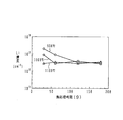
図4に、熱処理時間とLi濃度との関係を、熱処理温度別に示す。横軸は熱処理時間を単位「分」で表し、縦軸はLi濃度を単位「cm−3」で表す。ここで、Li濃度は、二次イオン質量分析法で得られた結果を、深さ方向に関して平均した値である。図中の丸記号、四角記号、及び三角記号は、それぞれ熱処理温度を900℃、1000℃、及び1100℃とした場合のLi濃度を示す。 FIG. 4 shows the relationship between the heat treatment time and the Li concentration for each heat treatment temperature. The horizontal axis represents the heat treatment time in the unit “minute”, and the vertical axis represents the Li concentration in the unit “cm −3 ”. Here, the Li concentration is a value obtained by averaging the results obtained by secondary ion mass spectrometry in the depth direction. The circle symbol, square symbol, and triangle symbol in the figure indicate the Li concentration when the heat treatment temperatures are 900 ° C., 1000 ° C., and 1100 ° C., respectively.
いずれの熱処理温度の場合にも、熱処理時間を十分長くすると、Li濃度を約3×1016cm−3まで低下させることができる。熱処理温度が1100℃の場合には、少なくとも30分でほぼ定常状態に達し、熱処理温度が1000℃の場合には、約50分で定常状態に達し、熱処理温度が900℃の場合には、約100分で定常状態に達する。後述するように、ZnO基板の上に発光素子を形成する場合には、基板中のLi濃度を4×1016cm−3以下にしておくことが好ましい。この要件を満たすために、熱処理温度900℃以上で熱処理時間100分以上、熱処理温度1000℃以上で熱処理時間50分以上、または熱処理温度1100℃以上で熱処理時間30分以上とすることが好ましい。 At any heat treatment temperature, if the heat treatment time is sufficiently long, the Li concentration can be reduced to about 3 × 10 16 cm −3 . When the heat treatment temperature is 1100 ° C., the steady state is reached in at least 30 minutes, when the heat treatment temperature is 1000 ° C., the steady state is reached in about 50 minutes, and when the heat treatment temperature is 900 ° C., about A steady state is reached in 100 minutes. As will be described later, when a light-emitting element is formed on a ZnO substrate, the Li concentration in the substrate is preferably 4 × 10 16 cm −3 or less. In order to satisfy this requirement, it is preferable that the heat treatment temperature is 900 ° C. or more and the heat treatment time is 100 minutes or more, the heat treatment temperature is 1000 ° C. or more and the heat treatment time is 50 minutes or more, or the heat treatment temperature is 1100 ° C. or more and the heat treatment time is 30 minutes or more.
基板上のZnO膜の電気的特性を評価するために、上記第1の実施例による方法で作製したZnO基板、及び従来の方法により作製したZnO基板の主表面上に、分子線エピタキシ(MBE)によりZnO膜を形成した。成膜時の基板温度は700℃である。 In order to evaluate the electrical characteristics of the ZnO film on the substrate, molecular beam epitaxy (MBE) is formed on the main surface of the ZnO substrate produced by the method according to the first embodiment and the ZnO substrate produced by the conventional method. Thus, a ZnO film was formed. The substrate temperature during film formation is 700 ° C.
図5に、ZnO膜中のLi濃度と電子移動度との関係を示す。Li濃度は、二次イオン質量分析法により測定し、電子移動度は、ファン・デル・ポー法により測定したホール係数から求めた。Li濃度が増大するに従って電子移動度が低下していることがわかる。Li濃度が2×1017cm−3以上になると、ZnO膜はほぼ絶縁性を示すようになる。 FIG. 5 shows the relationship between the Li concentration in the ZnO film and the electron mobility. The Li concentration was measured by secondary ion mass spectrometry, and the electron mobility was determined from the Hall coefficient measured by the van der Pau method. It can be seen that the electron mobility decreases as the Li concentration increases. When the Li concentration is 2 × 10 17 cm −3 or more, the ZnO film becomes substantially insulative.
ZnO膜を発光素子として用いる場合には、Li濃度を1×1016cm−3以下にすることが好ましい。この要請を満たすために、ZnO膜の成長温度が700℃の場合、ZnO基板中のLi濃度を4×1016cm−3以下にしておくことが好ましい。 When using a ZnO film as the light-emitting element, it is preferable that the Li concentration in 1 × 10 16 cm -3 or less. In order to satisfy this requirement, when the growth temperature of the ZnO film is 700 ° C., the Li concentration in the ZnO substrate is preferably 4 × 10 16 cm −3 or less.
上記第1の実施例では、ZnO基板の主表面が−c面である場合を取り扱ったが、ZnO基板の主表面が+c面である場合、第1の実施例と同様の方法を採用すると、熱処理中に主表面にステップバンチングが起こり、表面に1原子層以上の高さのステップが発生してしまう。次に説明する第2の実施例では、平坦な主表面を得ることを目的とする。 In the first embodiment, the case where the main surface of the ZnO substrate is the −c plane has been dealt with. However, when the main surface of the ZnO substrate is the + c plane, when the same method as the first embodiment is adopted, Step bunching occurs on the main surface during the heat treatment, and a step having a height of one atomic layer or more occurs on the surface. The second embodiment to be described next aims to obtain a flat main surface.
図6に、第2の実施例によるZnO基板の製造方法のフローチャートを示す。ステップST1からST3までは、第1の実施例の場合と同一である。ただし、第2の実施例で取り扱うZnO基板の主表面は+c面である。第2の実施例では、ステップST3において熱処理を行った後、ステップST4でアルカリ薬液による表面処理を行う。 FIG. 6 shows a flowchart of a method for manufacturing a ZnO substrate according to the second embodiment. Steps ST1 to ST3 are the same as those in the first embodiment. However, the main surface of the ZnO substrate handled in the second embodiment is the + c plane. In the second embodiment, after performing heat treatment in step ST3, surface treatment with an alkaline chemical is performed in step ST4.
アルカリ薬液として、エチレンジアミン四酢酸二水素二ナトリウム(EDTA溶液)とエチレンジアミンとの混合液を用いた。酸性のEDTA溶液にアルカリ性の液体であるエチレンジアミンを混ぜることにより、pHを調整することができる。濃度0.2mol/LのEDTAと濃度99%のエチレンジアミンとを体積比で20:1になるように混合した第1の薬液、及び体積比で10:1になるように混合した第2の薬液を調合し、第1の薬液及び第2の薬液でZnO基板の表面処理を行った。 As an alkaline chemical solution, a mixed solution of ethylenediaminetetraacetic acid disodium dihydrogen (EDTA solution) and ethylenediamine was used. The pH can be adjusted by mixing ethylenediamine, which is an alkaline liquid, into the acidic EDTA solution. A first chemical solution in which EDTA with a concentration of 0.2 mol / L and ethylenediamine with a concentration of 99% are mixed at a volume ratio of 20: 1, and a second chemical solution with a volume ratio of 10: 1. The ZnO substrate was surface-treated with the first chemical solution and the second chemical solution.
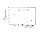
また、比較のために、濃度25%のテトラメチルアンモニウムヒドロキシド(TMAH)、濃度4%の塩酸、及び濃度8%のリン酸を用いて表面処理を行った。 For comparison, surface treatment was performed using tetramethylammonium hydroxide (TMAH) having a concentration of 25%, hydrochloric acid having a concentration of 4%, and phosphoric acid having a concentration of 8%.
図7に、各薬液によるZnOのエッチング速度を示す。横軸は薬液の種類に対応し、縦軸はエッチング速度を単位「nm/分」で表す。塩酸及びリン酸を用いて、室温で30分間のエッチングを行うと、ZnO基板の表面に正六角形のエッチピットが多数形成された。これは、ZnOが、酸に対して異方性のエッチング特性を示すためである。酸性薬液を用いると、アルカリ薬液を用いる場合に比べて、エッチング速度が速くなるが、エッチピットが発生するため、ZnO基板の表面を平坦化することはできない。TMAHを用いた場合には、ZnO基板はほとんどエッチングされなかった。 FIG. 7 shows the etching rate of ZnO by each chemical solution. The horizontal axis corresponds to the type of chemical solution, and the vertical axis represents the etching rate in the unit of “nm / min”. When etching was performed at room temperature for 30 minutes using hydrochloric acid and phosphoric acid, many regular hexagonal etch pits were formed on the surface of the ZnO substrate. This is because ZnO exhibits an anisotropic etching characteristic with respect to acid. When an acidic chemical solution is used, the etching rate is faster than when an alkaline chemical solution is used, but etch pits are generated, so that the surface of the ZnO substrate cannot be planarized. When TMAH was used, the ZnO substrate was hardly etched.
第1の薬液を用いて、室温で1時間のエッチングを行うことにより、エッチピットの形成されない平坦な表面を得ることができた。エチレンジアミンの濃度を高めたアルカリ性の強い第2の薬液を用いると、エッチング速度が速くなるが、表面の平坦性が悪くなる。表面の高い平坦性を維持するためには、EDTAとエチレンジアミンとの混合割合を、pHが7〜11の範囲内に収まるように調整することが好ましい。 By performing etching for 1 hour at room temperature using the first chemical solution, a flat surface on which no etch pits were formed could be obtained. When the second alkaline chemical solution having a high concentration of ethylenediamine is used, the etching rate is increased, but the flatness of the surface is deteriorated. In order to maintain high flatness of the surface, it is preferable to adjust the mixing ratio of EDTA and ethylenediamine so that the pH falls within the range of 7-11.
上記第2の実施例では、EDTAとエチレンジアミンとを混合した薬液を用いて表面の平坦化を行ったが、その他のpHが7〜11の薬液を用いてもよい。 In the said 2nd Example, although the surface planarization was performed using the chemical | medical solution which mixed EDTA and ethylenediamine, you may use the chemical | medical solution whose other pH is 7-11.
以上実施例に沿って本発明を説明したが、本発明はこれらに制限されるものではない。例えば、種々の変更、改良、組み合わせ等が可能なことは当業者に自明であろう。 Although the present invention has been described with reference to the embodiments, the present invention is not limited thereto. It will be apparent to those skilled in the art that various modifications, improvements, combinations, and the like can be made.
1 石英炉心管
2 ヒータ
3 坩堝
4 蓋
5 ZnO基板
1 Quartz
Claims (4)
(b)エチレンジアミン四酢酸二水素二ナトリウムとエチレンジアミンとの混合液を含むpHが7以上11以下のエッチング液を用いて、不純物であるLiが除去された前記基板の表層部をエッチングして平坦化する工程と
を有するZnO基板の製造方法。 (A) removing Li as an impurity from a substrate made of ZnO formed by a hydrothermal synthesis method;
(B) Etching and planarizing the surface layer portion of the substrate from which Li as an impurity has been removed , using an etching solution having a pH of 7 or more and 11 or less containing a mixed solution of disodium ethylenediaminetetraacetate and ethylenediamine . A method for manufacturing a ZnO substrate.
前記工程bにおいて、前記主表面を平坦化する請求項1に記載のZnO基板の製造方法。 The step a includes a step of performing a heat treatment in a state where the main surface of the substrate is in contact with a member made of ZnO,
The method for manufacturing a ZnO substrate according to claim 1 , wherein in the step b, the main surface is planarized.
Priority Applications (2)
| Application Number | Priority Date | Filing Date | Title |
|---|---|---|---|
| JP2005180990A JP4610422B2 (en) | 2005-06-21 | 2005-06-21 | Manufacturing method of ZnO substrate |
| US11/392,863 US7288208B2 (en) | 2005-06-21 | 2006-03-29 | Method of manufacturing ZnO substrate from ZnO crystal formed by hydrothermal synthesis method |
Applications Claiming Priority (1)
| Application Number | Priority Date | Filing Date | Title |
|---|---|---|---|
| JP2005180990A JP4610422B2 (en) | 2005-06-21 | 2005-06-21 | Manufacturing method of ZnO substrate |
Publications (3)
| Publication Number | Publication Date |
|---|---|
| JP2007001787A JP2007001787A (en) | 2007-01-11 |
| JP2007001787A5 JP2007001787A5 (en) | 2008-07-24 |
| JP4610422B2 true JP4610422B2 (en) | 2011-01-12 |
Family
ID=37572344
Family Applications (1)
| Application Number | Title | Priority Date | Filing Date |
|---|---|---|---|
| JP2005180990A Expired - Fee Related JP4610422B2 (en) | 2005-06-21 | 2005-06-21 | Manufacturing method of ZnO substrate |
Country Status (2)
| Country | Link |
|---|---|
| US (1) | US7288208B2 (en) |
| JP (1) | JP4610422B2 (en) |
Families Citing this family (9)
| Publication number | Priority date | Publication date | Assignee | Title |
|---|---|---|---|---|
| JP4994235B2 (en) * | 2005-08-09 | 2012-08-08 | スタンレー電気株式会社 | ZnO crystal and method for growing the same, and method for manufacturing light-emitting element |
| JP4953879B2 (en) | 2007-03-29 | 2012-06-13 | スタンレー電気株式会社 | Semiconductor device, manufacturing method thereof, and template substrate |
| JP2009029688A (en) * | 2007-06-28 | 2009-02-12 | Rohm Co Ltd | ZnO-BASED SUBSTRATE AND METHOD FOR PROCESSING THE SAME |
| JP2010053017A (en) | 2008-04-04 | 2010-03-11 | Fukuda Crystal Laboratory | Zinc oxide single crystal and method for producing the same |
| JP5411681B2 (en) * | 2009-12-09 | 2014-02-12 | スタンレー電気株式会社 | Method for growing zinc oxide based semiconductor and method for manufacturing semiconductor light emitting device |
| GB201010915D0 (en) | 2010-06-28 | 2010-08-11 | Uni I Oslo | Process |
| JP5647881B2 (en) * | 2010-12-17 | 2015-01-07 | スタンレー電気株式会社 | Zinc oxide semiconductor growth method |
| JP5654910B2 (en) * | 2011-03-14 | 2015-01-14 | スタンレー電気株式会社 | Zinc oxide substrate processing method |
| JP5647922B2 (en) * | 2011-03-16 | 2015-01-07 | スタンレー電気株式会社 | Zinc oxide-based substrate processing method and substrate with growth layer |
Citations (3)
| Publication number | Priority date | Publication date | Assignee | Title |
|---|---|---|---|---|
| JPH10229212A (en) * | 1996-12-13 | 1998-08-25 | Canon Inc | Manufacturing method of photovoltaic element |
| JP2004315361A (en) * | 2003-04-03 | 2004-11-11 | Tokyo Denpa Co Ltd | Zinc oxide single crystal |
| JP2005039131A (en) * | 2003-07-17 | 2005-02-10 | National Institute For Materials Science | Method for processing zinc oxide monocrystal wafer |
Family Cites Families (30)
| Publication number | Priority date | Publication date | Assignee | Title |
|---|---|---|---|---|
| JP2793047B2 (en) | 1991-02-08 | 1998-09-03 | シャープ株式会社 | Still image recording and playback device |
| JPH0581787A (en) | 1991-09-20 | 1993-04-02 | Mita Ind Co Ltd | Recording device for recording medium |
| JPH05165935A (en) | 1991-10-18 | 1993-07-02 | Konica Corp | Image photographing device and image filing device |
| CA2081762C (en) | 1991-12-05 | 2002-08-13 | Henry D. Hendrix | Method and apparatus to improve a video signal |
| JPH05158778A (en) | 1991-12-09 | 1993-06-25 | Canon Inc | Picture information storage device |
| JP3561930B2 (en) | 1993-08-14 | 2004-09-08 | ソニー株式会社 | Recording method of image search ID signal, image search method, and recorded image reproduction device |
| JP3610084B2 (en) | 1993-11-19 | 2005-01-12 | キヤノン株式会社 | Recording device |
| WO1995016262A1 (en) | 1993-12-10 | 1995-06-15 | Sony Corporation | Data recording medium and data reproduction apparatus |
| JPH08106721A (en) | 1994-10-07 | 1996-04-23 | Sony Corp | Recording apparatus and reproducing apparatus for disc-like recording medium |
| KR100197585B1 (en) | 1995-01-16 | 1999-06-15 | 윤종용 | Apparatus for recording/reproducing image and audio information into/from a semiconductor memory |
| JPH08205014A (en) | 1995-01-31 | 1996-08-09 | Casio Comput Co Ltd | Electronic still camera |
| US5745643A (en) | 1995-04-06 | 1998-04-28 | Kabushiki Kaisha Toshiba | System for and method of reproducing playback data appropriately by the use of attribute information on the playback data |
| KR100371429B1 (en) | 1995-08-21 | 2003-03-15 | 마츠시타 덴끼 산교 가부시키가이샤 | Multimedia optical disk, reproduction apparatus and method for achieving variable scene development based on interactive control |
| TW436777B (en) | 1995-09-29 | 2001-05-28 | Matsushita Electric Ind Co Ltd | A method and an apparatus for reproducing bitstream having non-sequential system clock data seamlessly therebetween |
| JP3824699B2 (en) | 1996-03-15 | 2006-09-20 | パイオニア株式会社 | Information recording medium, recording apparatus and method thereof, reproducing apparatus and method thereof, and information processing apparatus and method |
| JP3437371B2 (en) | 1996-03-22 | 2003-08-18 | パイオニア株式会社 | Information recording device and information reproducing device |
| EP1134988A1 (en) | 1996-03-29 | 2001-09-19 | Matsushita Electric Industrial Co., Ltd. | Multimedia optical disc having improved interactive reproduction procedure, a reproduction apparatus and a method for such a disc |
| US20020054049A1 (en) | 1996-11-12 | 2002-05-09 | Kenji Toyoda | Image playback apparatus, image recording apparatus, and methods thereof |
| JPH09182013A (en) | 1996-12-19 | 1997-07-11 | Casio Comput Co Ltd | Electronic still camera |
| US6078727A (en) | 1997-09-17 | 2000-06-20 | Matsushita Electric Industrial Co., Ltd. | Optical disc, recording apparatus, and computer-readable recording medium |
| JPH11136613A (en) | 1997-10-31 | 1999-05-21 | Canon Inc | Image recording device and its method |
| JP3597689B2 (en) | 1998-01-21 | 2004-12-08 | 株式会社東芝 | Information recording medium and information recording medium processing device |
| EP2267720A3 (en) | 1998-02-23 | 2011-03-09 | Kabushiki Kaisha Toshiba | Information storage medium, information playback method and apparatus and information recording method |
| JP3389086B2 (en) | 1998-02-23 | 2003-03-24 | 株式会社東芝 | Optical disc recording method, optical disc, reproducing method, and reproducing apparatus |
| JP3356991B2 (en) | 1998-06-17 | 2002-12-16 | 株式会社日立製作所 | Optical disc, recording method, recording device, reproducing method, and reproducing device |
| US6721493B1 (en) | 1998-06-24 | 2004-04-13 | Samsung Electronics Co., Ltd. | Recording medium for storing information for still picture, recording and/or reproducing method and apparatus therefor |
| US6389222B1 (en) | 1998-07-07 | 2002-05-14 | Kabushiki Kaisha Toshiba | Management system for protected and temporarily-erased still picture information |
| JP3383587B2 (en) | 1998-07-07 | 2003-03-04 | 株式会社東芝 | Still image continuous information recording method, optical disc, optical disc information reproducing apparatus and information reproducing method |
| KR100326337B1 (en) | 1998-09-05 | 2002-09-12 | 엘지전자주식회사 | Generation and recording method of data reproduction order information on a rewritable recording medium |
| JP4045499B2 (en) | 2003-03-27 | 2008-02-13 | 信越半導体株式会社 | Method for manufacturing ZnO-based semiconductor element |
-
2005
- 2005-06-21 JP JP2005180990A patent/JP4610422B2/en not_active Expired - Fee Related
-
2006
- 2006-03-29 US US11/392,863 patent/US7288208B2/en active Active
Patent Citations (3)
| Publication number | Priority date | Publication date | Assignee | Title |
|---|---|---|---|---|
| JPH10229212A (en) * | 1996-12-13 | 1998-08-25 | Canon Inc | Manufacturing method of photovoltaic element |
| JP2004315361A (en) * | 2003-04-03 | 2004-11-11 | Tokyo Denpa Co Ltd | Zinc oxide single crystal |
| JP2005039131A (en) * | 2003-07-17 | 2005-02-10 | National Institute For Materials Science | Method for processing zinc oxide monocrystal wafer |
Also Published As
| Publication number | Publication date |
|---|---|
| JP2007001787A (en) | 2007-01-11 |
| US20060283834A1 (en) | 2006-12-21 |
| US7288208B2 (en) | 2007-10-30 |
Similar Documents
| Publication | Publication Date | Title |
|---|---|---|
| JP4610422B2 (en) | Manufacturing method of ZnO substrate | |
| JP7001660B2 (en) | Board structure designed for power and RF applications | |
| TWI326103B (en) | ||
| JP2006216826A (en) | Manufacturing method of soi wafer | |
| US20090291523A1 (en) | Method of Manufacturing High Quality ZnO Monocrystal Film on Silicon(111) Substrate | |
| US8906786B2 (en) | Method for producing single crystal SiC substrate and single crystal SiC substrate produced by the same | |
| JP2009149481A (en) | Method for manufacturing semiconductor substrate | |
| JP2009272471A (en) | Bonded wafer manufacturing method | |
| JP2009049411A (en) | Method for manufacturing ssoi substrate | |
| WO2011151968A1 (en) | Method for manufacturing bonded wafer | |
| JP5625239B2 (en) | Manufacturing method of bonded wafer | |
| JP5310004B2 (en) | Manufacturing method of bonded wafer | |
| JP2008263025A (en) | Manufacturing method of semiconductor substrate | |
| JP5205840B2 (en) | Manufacturing method of semiconductor substrate | |
| JP6280301B2 (en) | Epitaxial silicon wafer manufacturing method, epitaxial silicon wafer, and solid-state imaging device manufacturing method | |
| KR20230013132A (en) | Pre-cleaning and encapsulation of microLED features | |
| TW200844276A (en) | Monocrystal zinc oxide substrate | |
| JP4733729B2 (en) | ZnTe compound semiconductor surface treatment method and semiconductor device manufacturing method | |
| JP6361779B2 (en) | Epitaxial silicon wafer manufacturing method, epitaxial silicon wafer, and solid-state imaging device manufacturing method | |
| JP2012064802A (en) | Manufacturing method for bonded wafer | |
| JP2009302097A (en) | Method of manufacturing single crystal sic substrate, and single crystal sic substrate | |
| JP2012015394A (en) | AlGaAs SUBSTRATE, EPITAXIAL WAFER FOR INFRARED LED, AND INFRARED LED | |
| JP2010258134A (en) | Method of manufacturing quantum well structure, semiconductor laser, and compound semiconductor layer, and method of controlling mbe (molecular beam epitaxy) device | |
| JP2011134983A (en) | Method of manufacturing silicon semiconductor substrate | |
| JP2011138956A (en) | Method of manufacturing silicon semiconductor substrate |
Legal Events
| Date | Code | Title | Description |
|---|---|---|---|
| A521 | Request for written amendment filed |
Free format text: JAPANESE INTERMEDIATE CODE: A523 Effective date: 20080609 |
|
| A621 | Written request for application examination |
Free format text: JAPANESE INTERMEDIATE CODE: A621 Effective date: 20080609 |
|
| A977 | Report on retrieval |
Free format text: JAPANESE INTERMEDIATE CODE: A971007 Effective date: 20100420 |
|
| A131 | Notification of reasons for refusal |
Free format text: JAPANESE INTERMEDIATE CODE: A131 Effective date: 20100427 |
|
| A521 | Request for written amendment filed |
Free format text: JAPANESE INTERMEDIATE CODE: A523 Effective date: 20100531 |
|
| TRDD | Decision of grant or rejection written | ||
| A01 | Written decision to grant a patent or to grant a registration (utility model) |
Free format text: JAPANESE INTERMEDIATE CODE: A01 Effective date: 20101005 |
|
| A01 | Written decision to grant a patent or to grant a registration (utility model) |
Free format text: JAPANESE INTERMEDIATE CODE: A01 |
|
| A61 | First payment of annual fees (during grant procedure) |
Free format text: JAPANESE INTERMEDIATE CODE: A61 Effective date: 20101012 |
|
| FPAY | Renewal fee payment (event date is renewal date of database) |
Free format text: PAYMENT UNTIL: 20131022 Year of fee payment: 3 |
|
| R150 | Certificate of patent or registration of utility model |
Ref document number: 4610422 Country of ref document: JP Free format text: JAPANESE INTERMEDIATE CODE: R150 Free format text: JAPANESE INTERMEDIATE CODE: R150 |
|
| R250 | Receipt of annual fees |
Free format text: JAPANESE INTERMEDIATE CODE: R250 |
|
| R250 | Receipt of annual fees |
Free format text: JAPANESE INTERMEDIATE CODE: R250 |
|
| R250 | Receipt of annual fees |
Free format text: JAPANESE INTERMEDIATE CODE: R250 |
|
| R250 | Receipt of annual fees |
Free format text: JAPANESE INTERMEDIATE CODE: R250 |
|
| R250 | Receipt of annual fees |
Free format text: JAPANESE INTERMEDIATE CODE: R250 |
|
| R250 | Receipt of annual fees |
Free format text: JAPANESE INTERMEDIATE CODE: R250 |
|
| R250 | Receipt of annual fees |
Free format text: JAPANESE INTERMEDIATE CODE: R250 |
|
| R250 | Receipt of annual fees |
Free format text: JAPANESE INTERMEDIATE CODE: R250 |
|
| LAPS | Cancellation because of no payment of annual fees |