JP4601843B2 - Light emitting device - Google Patents
Light emitting device Download PDFInfo
- Publication number
- JP4601843B2 JP4601843B2 JP2001056033A JP2001056033A JP4601843B2 JP 4601843 B2 JP4601843 B2 JP 4601843B2 JP 2001056033 A JP2001056033 A JP 2001056033A JP 2001056033 A JP2001056033 A JP 2001056033A JP 4601843 B2 JP4601843 B2 JP 4601843B2
- Authority
- JP
- Japan
- Prior art keywords
- film
- light
- emitting device
- electrode
- light emitting
- Prior art date
- Legal status (The legal status is an assumption and is not a legal conclusion. Google has not performed a legal analysis and makes no representation as to the accuracy of the status listed.)
- Expired - Fee Related
Links
- 239000000463 material Substances 0.000 claims description 52
- 230000015572 biosynthetic process Effects 0.000 claims description 23
- 229920005989 resin Polymers 0.000 claims description 16
- 239000011347 resin Substances 0.000 claims description 16
- 229910010272 inorganic material Inorganic materials 0.000 claims description 10
- 239000011147 inorganic material Substances 0.000 claims description 10
- 229920001940 conductive polymer Polymers 0.000 claims description 9
- 239000010408 film Substances 0.000 description 163
- 238000005401 electroluminescence Methods 0.000 description 115
- 239000010410 layer Substances 0.000 description 69
- 239000000758 substrate Substances 0.000 description 52
- 238000000034 method Methods 0.000 description 21
- 238000012546 transfer Methods 0.000 description 19
- 229910052751 metal Inorganic materials 0.000 description 18
- 239000002184 metal Substances 0.000 description 18
- 239000004065 semiconductor Substances 0.000 description 14
- 229910052581 Si3N4 Inorganic materials 0.000 description 13
- HQVNEWCFYHHQES-UHFFFAOYSA-N silicon nitride Chemical compound N12[Si]34N5[Si]62N3[Si]51N64 HQVNEWCFYHHQES-UHFFFAOYSA-N 0.000 description 13
- 238000002347 injection Methods 0.000 description 11
- 239000007924 injection Substances 0.000 description 11
- 239000000853 adhesive Substances 0.000 description 10
- 230000001070 adhesive effect Effects 0.000 description 10
- 239000007789 gas Substances 0.000 description 10
- 239000011229 interlayer Substances 0.000 description 10
- 239000002985 plastic film Substances 0.000 description 10
- 238000007789 sealing Methods 0.000 description 10
- 238000007740 vapor deposition Methods 0.000 description 10
- IJGRMHOSHXDMSA-UHFFFAOYSA-N Atomic nitrogen Chemical compound N#N IJGRMHOSHXDMSA-UHFFFAOYSA-N 0.000 description 9
- 229910052782 aluminium Inorganic materials 0.000 description 9
- XAGFODPZIPBFFR-UHFFFAOYSA-N aluminium Chemical compound [Al] XAGFODPZIPBFFR-UHFFFAOYSA-N 0.000 description 9
- 238000004519 manufacturing process Methods 0.000 description 9
- 229920006255 plastic film Polymers 0.000 description 9
- -1 polyethylene Polymers 0.000 description 9
- VYPSYNLAJGMNEJ-UHFFFAOYSA-N silicon dioxide Inorganic materials O=[Si]=O VYPSYNLAJGMNEJ-UHFFFAOYSA-N 0.000 description 9
- BASFCYQUMIYNBI-UHFFFAOYSA-N platinum Chemical compound [Pt] BASFCYQUMIYNBI-UHFFFAOYSA-N 0.000 description 8
- 238000012545 processing Methods 0.000 description 8
- XUIMIQQOPSSXEZ-UHFFFAOYSA-N Silicon Chemical compound [Si] XUIMIQQOPSSXEZ-UHFFFAOYSA-N 0.000 description 7
- 239000003990 capacitor Substances 0.000 description 7
- 238000001704 evaporation Methods 0.000 description 7
- 230000007246 mechanism Effects 0.000 description 7
- 229910052710 silicon Inorganic materials 0.000 description 7
- 239000010703 silicon Substances 0.000 description 7
- 229910052814 silicon oxide Inorganic materials 0.000 description 7
- PXHVJJICTQNCMI-UHFFFAOYSA-N Nickel Chemical compound [Ni] PXHVJJICTQNCMI-UHFFFAOYSA-N 0.000 description 6
- 229910052736 halogen Inorganic materials 0.000 description 6
- 239000012298 atmosphere Substances 0.000 description 5
- OMRRUNXAWXNVFW-UHFFFAOYSA-N fluoridochlorine Chemical compound ClF OMRRUNXAWXNVFW-UHFFFAOYSA-N 0.000 description 5
- 239000011521 glass Substances 0.000 description 5
- 238000010438 heat treatment Methods 0.000 description 5
- 239000004033 plastic Substances 0.000 description 5
- 229920003023 plastic Polymers 0.000 description 5
- 125000006850 spacer group Chemical group 0.000 description 5
- 239000000126 substance Substances 0.000 description 5
- JOHWNGGYGAVMGU-UHFFFAOYSA-N trifluorochlorine Chemical compound FCl(F)F JOHWNGGYGAVMGU-UHFFFAOYSA-N 0.000 description 5
- XKRFYHLGVUSROY-UHFFFAOYSA-N Argon Chemical compound [Ar] XKRFYHLGVUSROY-UHFFFAOYSA-N 0.000 description 4
- OKTJSMMVPCPJKN-UHFFFAOYSA-N Carbon Chemical compound [C] OKTJSMMVPCPJKN-UHFFFAOYSA-N 0.000 description 4
- WHXSMMKQMYFTQS-UHFFFAOYSA-N Lithium Chemical compound [Li] WHXSMMKQMYFTQS-UHFFFAOYSA-N 0.000 description 4
- 238000000137 annealing Methods 0.000 description 4
- QVGXLLKOCUKJST-UHFFFAOYSA-N atomic oxygen Chemical compound [O] QVGXLLKOCUKJST-UHFFFAOYSA-N 0.000 description 4
- 229910052799 carbon Inorganic materials 0.000 description 4
- 239000011651 chromium Substances 0.000 description 4
- 229910021419 crystalline silicon Inorganic materials 0.000 description 4
- 239000002019 doping agent Substances 0.000 description 4
- 229910052744 lithium Inorganic materials 0.000 description 4
- PQXKHYXIUOZZFA-UHFFFAOYSA-M lithium fluoride Chemical compound [Li+].[F-] PQXKHYXIUOZZFA-UHFFFAOYSA-M 0.000 description 4
- 239000001301 oxygen Substances 0.000 description 4
- 229910052760 oxygen Inorganic materials 0.000 description 4
- 230000000737 periodic effect Effects 0.000 description 4
- 229920000642 polymer Polymers 0.000 description 4
- 239000003566 sealing material Substances 0.000 description 4
- 238000004544 sputter deposition Methods 0.000 description 4
- UHOVQNZJYSORNB-UHFFFAOYSA-N Benzene Chemical compound C1=CC=CC=C1 UHOVQNZJYSORNB-UHFFFAOYSA-N 0.000 description 3
- 230000004913 activation Effects 0.000 description 3
- 229910021417 amorphous silicon Inorganic materials 0.000 description 3
- MZJUGRUTVANEDW-UHFFFAOYSA-N bromine fluoride Chemical compound BrF MZJUGRUTVANEDW-UHFFFAOYSA-N 0.000 description 3
- 229910001873 dinitrogen Inorganic materials 0.000 description 3
- 239000000428 dust Substances 0.000 description 3
- 230000008020 evaporation Effects 0.000 description 3
- 230000005284 excitation Effects 0.000 description 3
- RBTKNAXYKSUFRK-UHFFFAOYSA-N heliogen blue Chemical compound [Cu].[N-]1C2=C(C=CC=C3)C3=C1N=C([N-]1)C3=CC=CC=C3C1=NC([N-]1)=C(C=CC=C3)C3=C1N=C([N-]1)C3=CC=CC=C3C1=N2 RBTKNAXYKSUFRK-UHFFFAOYSA-N 0.000 description 3
- 238000005984 hydrogenation reaction Methods 0.000 description 3
- 239000012535 impurity Substances 0.000 description 3
- 239000011261 inert gas Substances 0.000 description 3
- 229910052757 nitrogen Inorganic materials 0.000 description 3
- 238000002161 passivation Methods 0.000 description 3
- 238000005268 plasma chemical vapour deposition Methods 0.000 description 3
- 229910052697 platinum Inorganic materials 0.000 description 3
- 229920001721 polyimide Polymers 0.000 description 3
- 230000001681 protective effect Effects 0.000 description 3
- 230000004044 response Effects 0.000 description 3
- 238000003860 storage Methods 0.000 description 3
- CXWXQJXEFPUFDZ-UHFFFAOYSA-N tetralin Chemical compound C1=CC=C2CCCCC2=C1 CXWXQJXEFPUFDZ-UHFFFAOYSA-N 0.000 description 3
- WFKWXMTUELFFGS-UHFFFAOYSA-N tungsten Chemical compound [W] WFKWXMTUELFFGS-UHFFFAOYSA-N 0.000 description 3
- 229910052721 tungsten Inorganic materials 0.000 description 3
- 239000010937 tungsten Substances 0.000 description 3
- INJJUVRCCVMHPA-UHFFFAOYSA-N 2-dodecan-3-ylthiophene Chemical compound CCCCCCCCCC(CC)C1=CC=CS1 INJJUVRCCVMHPA-UHFFFAOYSA-N 0.000 description 2
- JJQBWCOFORHRQI-UHFFFAOYSA-N 2-hexan-3-ylthiophene Chemical compound CCCC(CC)C1=CC=CS1 JJQBWCOFORHRQI-UHFFFAOYSA-N 0.000 description 2
- CRFAKQQUNCZMID-UHFFFAOYSA-N 2-octadecan-3-ylthiophene Chemical compound CCCCCCCCCCCCCCCC(CC)C1=CC=CS1 CRFAKQQUNCZMID-UHFFFAOYSA-N 0.000 description 2
- LCCZHWHVBHKPCD-UHFFFAOYSA-N 2-octan-3-ylthiophene Chemical compound CCCCCC(CC)C1=CC=CS1 LCCZHWHVBHKPCD-UHFFFAOYSA-N 0.000 description 2
- 229920000178 Acrylic resin Polymers 0.000 description 2
- KYXNZHWESMSPDE-UHFFFAOYSA-N CCCCCCCCCCCCCCCCCC(CC)C1=CC=CS1 Chemical compound CCCCCCCCCCCCCCCCCC(CC)C1=CC=CS1 KYXNZHWESMSPDE-UHFFFAOYSA-N 0.000 description 2
- HEDRZPFGACZZDS-UHFFFAOYSA-N Chloroform Chemical compound ClC(Cl)Cl HEDRZPFGACZZDS-UHFFFAOYSA-N 0.000 description 2
- VYZAMTAEIAYCRO-UHFFFAOYSA-N Chromium Chemical compound [Cr] VYZAMTAEIAYCRO-UHFFFAOYSA-N 0.000 description 2
- FYYHWMGAXLPEAU-UHFFFAOYSA-N Magnesium Chemical compound [Mg] FYYHWMGAXLPEAU-UHFFFAOYSA-N 0.000 description 2
- 239000004952 Polyamide Substances 0.000 description 2
- 239000004642 Polyimide Substances 0.000 description 2
- ZLMJMSJWJFRBEC-UHFFFAOYSA-N Potassium Chemical compound [K] ZLMJMSJWJFRBEC-UHFFFAOYSA-N 0.000 description 2
- NRCMAYZCPIVABH-UHFFFAOYSA-N Quinacridone Chemical compound N1C2=CC=CC=C2C(=O)C2=C1C=C1C(=O)C3=CC=CC=C3NC1=C2 NRCMAYZCPIVABH-UHFFFAOYSA-N 0.000 description 2
- YTPLMLYBLZKORZ-UHFFFAOYSA-N Thiophene Chemical compound C=1C=CSC=1 YTPLMLYBLZKORZ-UHFFFAOYSA-N 0.000 description 2
- RTAQQCXQSZGOHL-UHFFFAOYSA-N Titanium Chemical compound [Ti] RTAQQCXQSZGOHL-UHFFFAOYSA-N 0.000 description 2
- XLOMVQKBTHCTTD-UHFFFAOYSA-N Zinc monoxide Chemical compound [Zn]=O XLOMVQKBTHCTTD-UHFFFAOYSA-N 0.000 description 2
- NIXOWILDQLNWCW-UHFFFAOYSA-N acrylic acid group Chemical group C(C=C)(=O)O NIXOWILDQLNWCW-UHFFFAOYSA-N 0.000 description 2
- MWPLVEDNUUSJAV-UHFFFAOYSA-N anthracene Chemical class C1=CC=CC2=CC3=CC=CC=C3C=C21 MWPLVEDNUUSJAV-UHFFFAOYSA-N 0.000 description 2
- 229910052786 argon Inorganic materials 0.000 description 2
- QVQLCTNNEUAWMS-UHFFFAOYSA-N barium oxide Chemical compound [Ba]=O QVQLCTNNEUAWMS-UHFFFAOYSA-N 0.000 description 2
- 230000008901 benefit Effects 0.000 description 2
- 239000000919 ceramic Substances 0.000 description 2
- 229910052804 chromium Inorganic materials 0.000 description 2
- 150000001875 compounds Chemical class 0.000 description 2
- 229920000547 conjugated polymer Polymers 0.000 description 2
- XCJYREBRNVKWGJ-UHFFFAOYSA-N copper(II) phthalocyanine Chemical compound [Cu+2].C12=CC=CC=C2C(N=C2[N-]C(C3=CC=CC=C32)=N2)=NC1=NC([C]1C=CC=CC1=1)=NC=1N=C1[C]3C=CC=CC3=C2[N-]1 XCJYREBRNVKWGJ-UHFFFAOYSA-N 0.000 description 2
- VBVAVBCYMYWNOU-UHFFFAOYSA-N coumarin 6 Chemical compound C1=CC=C2SC(C3=CC4=CC=C(C=C4OC3=O)N(CC)CC)=NC2=C1 VBVAVBCYMYWNOU-UHFFFAOYSA-N 0.000 description 2
- 239000003085 diluting agent Substances 0.000 description 2
- 230000000694 effects Effects 0.000 description 2
- 239000003822 epoxy resin Substances 0.000 description 2
- 229910052732 germanium Inorganic materials 0.000 description 2
- GNPVGFCGXDBREM-UHFFFAOYSA-N germanium atom Chemical compound [Ge] GNPVGFCGXDBREM-UHFFFAOYSA-N 0.000 description 2
- 229910003437 indium oxide Inorganic materials 0.000 description 2
- PJXISJQVUVHSOJ-UHFFFAOYSA-N indium(iii) oxide Chemical compound [O-2].[O-2].[O-2].[In+3].[In+3] PJXISJQVUVHSOJ-UHFFFAOYSA-N 0.000 description 2
- PDJAZCSYYQODQF-UHFFFAOYSA-N iodine monofluoride Chemical compound IF PDJAZCSYYQODQF-UHFFFAOYSA-N 0.000 description 2
- 150000002500 ions Chemical class 0.000 description 2
- 239000004973 liquid crystal related substance Substances 0.000 description 2
- 239000011777 magnesium Substances 0.000 description 2
- 239000011159 matrix material Substances 0.000 description 2
- 229910052759 nickel Inorganic materials 0.000 description 2
- 239000011368 organic material Substances 0.000 description 2
- 229920003227 poly(N-vinyl carbazole) Polymers 0.000 description 2
- 229920003207 poly(ethylene-2,6-naphthalate) Polymers 0.000 description 2
- 229920006122 polyamide resin Polymers 0.000 description 2
- 229920000767 polyaniline Polymers 0.000 description 2
- 239000004417 polycarbonate Substances 0.000 description 2
- 229920000647 polyepoxide Polymers 0.000 description 2
- 239000011112 polyethylene naphthalate Substances 0.000 description 2
- 229920000139 polyethylene terephthalate Polymers 0.000 description 2
- 239000005020 polyethylene terephthalate Substances 0.000 description 2
- 229920000123 polythiophene Polymers 0.000 description 2
- 229910052700 potassium Inorganic materials 0.000 description 2
- 239000011591 potassium Substances 0.000 description 2
- 238000007781 pre-processing Methods 0.000 description 2
- 230000008569 process Effects 0.000 description 2
- 239000010453 quartz Substances 0.000 description 2
- 239000000565 sealant Substances 0.000 description 2
- 238000002230 thermal chemical vapour deposition Methods 0.000 description 2
- 229920001187 thermosetting polymer Polymers 0.000 description 2
- 239000010409 thin film Substances 0.000 description 2
- 239000010936 titanium Substances 0.000 description 2
- 229910052719 titanium Inorganic materials 0.000 description 2
- JEOQACOXAOEPLX-WCCKRBBISA-N (2s)-2-amino-5-(diaminomethylideneamino)pentanoic acid;1,3-thiazolidine-4-carboxylic acid Chemical compound OC(=O)C1CSCN1.OC(=O)[C@@H](N)CCCN=C(N)N JEOQACOXAOEPLX-WCCKRBBISA-N 0.000 description 1
- DTZWGKCFKSJGPK-VOTSOKGWSA-N (e)-2-(2-methyl-6-(2-(1,1,7,7-tetramethyl-1,2,3,5,6,7-hexahydropyrido[3,2,1-ij]quinolin-9-yl)vinyl)-4h-pyran-4-ylidene)malononitrile Chemical compound O1C(C)=CC(=C(C#N)C#N)C=C1\C=C\C1=CC(C(CCN2CCC3(C)C)(C)C)=C2C3=C1 DTZWGKCFKSJGPK-VOTSOKGWSA-N 0.000 description 1
- POILWHVDKZOXJZ-ARJAWSKDSA-M (z)-4-oxopent-2-en-2-olate Chemical compound C\C([O-])=C\C(C)=O POILWHVDKZOXJZ-ARJAWSKDSA-M 0.000 description 1
- NBYLBWHHTUWMER-UHFFFAOYSA-N 2-Methylquinolin-8-ol Chemical class C1=CC=C(O)C2=NC(C)=CC=C21 NBYLBWHHTUWMER-UHFFFAOYSA-N 0.000 description 1
- YLYPIBBGWLKELC-RMKNXTFCSA-N 2-[2-[(e)-2-[4-(dimethylamino)phenyl]ethenyl]-6-methylpyran-4-ylidene]propanedinitrile Chemical compound C1=CC(N(C)C)=CC=C1\C=C\C1=CC(=C(C#N)C#N)C=C(C)O1 YLYPIBBGWLKELC-RMKNXTFCSA-N 0.000 description 1
- ROTNFTXFUKFPHE-UHFFFAOYSA-N 2-butan-2-ylthiophene Chemical compound CCC(C)C1=CC=CS1 ROTNFTXFUKFPHE-UHFFFAOYSA-N 0.000 description 1
- QENGPZGAWFQWCZ-UHFFFAOYSA-N 3-Methylthiophene Chemical compound CC=1C=CSC=1 QENGPZGAWFQWCZ-UHFFFAOYSA-N 0.000 description 1
- SLDBAXYJAIRQMX-UHFFFAOYSA-N 3-ethylthiophene Chemical compound CCC=1C=CSC=1 SLDBAXYJAIRQMX-UHFFFAOYSA-N 0.000 description 1
- ZNJRONVKWRHYBF-VOTSOKGWSA-N 4-(dicyanomethylene)-2-methyl-6-julolidyl-9-enyl-4h-pyran Chemical compound O1C(C)=CC(=C(C#N)C#N)C=C1\C=C\C1=CC(CCCN2CCC3)=C2C3=C1 ZNJRONVKWRHYBF-VOTSOKGWSA-N 0.000 description 1
- ZCYVEMRRCGMTRW-UHFFFAOYSA-N 7553-56-2 Chemical compound [I] ZCYVEMRRCGMTRW-UHFFFAOYSA-N 0.000 description 1
- 229910001316 Ag alloy Inorganic materials 0.000 description 1
- ZOXJGFHDIHLPTG-UHFFFAOYSA-N Boron Chemical compound [B] ZOXJGFHDIHLPTG-UHFFFAOYSA-N 0.000 description 1
- WKBOTKDWSSQWDR-UHFFFAOYSA-N Bromine atom Chemical compound [Br] WKBOTKDWSSQWDR-UHFFFAOYSA-N 0.000 description 1
- OYPRJOBELJOOCE-UHFFFAOYSA-N Calcium Chemical compound [Ca] OYPRJOBELJOOCE-UHFFFAOYSA-N 0.000 description 1
- RYGMFSIKBFXOCR-UHFFFAOYSA-N Copper Chemical compound [Cu] RYGMFSIKBFXOCR-UHFFFAOYSA-N 0.000 description 1
- YMWUJEATGCHHMB-UHFFFAOYSA-N Dichloromethane Chemical compound ClCCl YMWUJEATGCHHMB-UHFFFAOYSA-N 0.000 description 1
- PXGOKWXKJXAPGV-UHFFFAOYSA-N Fluorine Chemical compound FF PXGOKWXKJXAPGV-UHFFFAOYSA-N 0.000 description 1
- UFHFLCQGNIYNRP-UHFFFAOYSA-N Hydrogen Chemical compound [H][H] UFHFLCQGNIYNRP-UHFFFAOYSA-N 0.000 description 1
- DGAQECJNVWCQMB-PUAWFVPOSA-M Ilexoside XXIX Chemical compound C[C@@H]1CC[C@@]2(CC[C@@]3(C(=CC[C@H]4[C@]3(CC[C@@H]5[C@@]4(CC[C@@H](C5(C)C)OS(=O)(=O)[O-])C)C)[C@@H]2[C@]1(C)O)C)C(=O)O[C@H]6[C@@H]([C@H]([C@@H]([C@H](O6)CO)O)O)O.[Na+] DGAQECJNVWCQMB-PUAWFVPOSA-M 0.000 description 1
- 229910000861 Mg alloy Inorganic materials 0.000 description 1
- ISWSIDIOOBJBQZ-UHFFFAOYSA-N Phenol Chemical class OC1=CC=CC=C1 ISWSIDIOOBJBQZ-UHFFFAOYSA-N 0.000 description 1
- 229920001609 Poly(3,4-ethylenedioxythiophene) Polymers 0.000 description 1
- 239000004698 Polyethylene Substances 0.000 description 1
- 238000001069 Raman spectroscopy Methods 0.000 description 1
- BQCADISMDOOEFD-UHFFFAOYSA-N Silver Chemical compound [Ag] BQCADISMDOOEFD-UHFFFAOYSA-N 0.000 description 1
- 229910001080 W alloy Inorganic materials 0.000 description 1
- HSFWRNGVRCDJHI-UHFFFAOYSA-N alpha-acetylene Natural products C#C HSFWRNGVRCDJHI-UHFFFAOYSA-N 0.000 description 1
- 239000010405 anode material Substances 0.000 description 1
- 229910052788 barium Inorganic materials 0.000 description 1
- DSAJWYNOEDNPEQ-UHFFFAOYSA-N barium atom Chemical compound [Ba] DSAJWYNOEDNPEQ-UHFFFAOYSA-N 0.000 description 1
- 229910052790 beryllium Inorganic materials 0.000 description 1
- ATBAMAFKBVZNFJ-UHFFFAOYSA-N beryllium atom Chemical compound [Be] ATBAMAFKBVZNFJ-UHFFFAOYSA-N 0.000 description 1
- UFVXQDWNSAGPHN-UHFFFAOYSA-K bis[(2-methylquinolin-8-yl)oxy]-(4-phenylphenoxy)alumane Chemical compound [Al+3].C1=CC=C([O-])C2=NC(C)=CC=C21.C1=CC=C([O-])C2=NC(C)=CC=C21.C1=CC([O-])=CC=C1C1=CC=CC=C1 UFVXQDWNSAGPHN-UHFFFAOYSA-K 0.000 description 1
- 229910052796 boron Inorganic materials 0.000 description 1
- GDTBXPJZTBHREO-UHFFFAOYSA-N bromine Substances BrBr GDTBXPJZTBHREO-UHFFFAOYSA-N 0.000 description 1
- 229910052794 bromium Inorganic materials 0.000 description 1
- 229910052792 caesium Inorganic materials 0.000 description 1
- TVFDJXOCXUVLDH-UHFFFAOYSA-N caesium atom Chemical compound [Cs] TVFDJXOCXUVLDH-UHFFFAOYSA-N 0.000 description 1
- 229910052791 calcium Inorganic materials 0.000 description 1
- 239000011575 calcium Substances 0.000 description 1
- 239000000969 carrier Substances 0.000 description 1
- 238000006243 chemical reaction Methods 0.000 description 1
- 238000010549 co-Evaporation Methods 0.000 description 1
- 238000000576 coating method Methods 0.000 description 1
- 229910052802 copper Inorganic materials 0.000 description 1
- 239000010949 copper Substances 0.000 description 1
- 238000002425 crystallisation Methods 0.000 description 1
- 230000008025 crystallization Effects 0.000 description 1
- 230000007423 decrease Effects 0.000 description 1
- 230000007547 defect Effects 0.000 description 1
- 238000000151 deposition Methods 0.000 description 1
- 230000008021 deposition Effects 0.000 description 1
- 230000006866 deterioration Effects 0.000 description 1
- 238000011161 development Methods 0.000 description 1
- 238000010586 diagram Methods 0.000 description 1
- 238000010790 dilution Methods 0.000 description 1
- 239000012895 dilution Substances 0.000 description 1
- 239000006185 dispersion Substances 0.000 description 1
- 238000009826 distribution Methods 0.000 description 1
- 238000010894 electron beam technology Methods 0.000 description 1
- 238000005530 etching Methods 0.000 description 1
- 229920002457 flexible plastic Polymers 0.000 description 1
- 229910052731 fluorine Inorganic materials 0.000 description 1
- 239000011737 fluorine Substances 0.000 description 1
- 150000002367 halogens Chemical group 0.000 description 1
- 239000001307 helium Substances 0.000 description 1
- 229910052734 helium Inorganic materials 0.000 description 1
- SWQJXJOGLNCZEY-UHFFFAOYSA-N helium atom Chemical compound [He] SWQJXJOGLNCZEY-UHFFFAOYSA-N 0.000 description 1
- 238000004770 highest occupied molecular orbital Methods 0.000 description 1
- 230000005525 hole transport Effects 0.000 description 1
- 239000001257 hydrogen Substances 0.000 description 1
- 229910052739 hydrogen Inorganic materials 0.000 description 1
- 239000012212 insulator Substances 0.000 description 1
- 229910052740 iodine Inorganic materials 0.000 description 1
- 239000011630 iodine Substances 0.000 description 1
- VJUJMLSNVYZCDT-UHFFFAOYSA-N iodine trifluoride Chemical compound FI(F)F VJUJMLSNVYZCDT-UHFFFAOYSA-N 0.000 description 1
- 230000001678 irradiating effect Effects 0.000 description 1
- 238000010030 laminating Methods 0.000 description 1
- 238000005224 laser annealing Methods 0.000 description 1
- 239000003446 ligand Substances 0.000 description 1
- 229910052749 magnesium Inorganic materials 0.000 description 1
- 238000012423 maintenance Methods 0.000 description 1
- 229910052754 neon Inorganic materials 0.000 description 1
- GKAOGPIIYCISHV-UHFFFAOYSA-N neon atom Chemical compound [Ne] GKAOGPIIYCISHV-UHFFFAOYSA-N 0.000 description 1
- VOFUROIFQGPCGE-UHFFFAOYSA-N nile red Chemical compound C1=CC=C2C3=NC4=CC=C(N(CC)CC)C=C4OC3=CC(=O)C2=C1 VOFUROIFQGPCGE-UHFFFAOYSA-N 0.000 description 1
- 239000012299 nitrogen atmosphere Substances 0.000 description 1
- 239000003921 oil Substances 0.000 description 1
- 230000003287 optical effect Effects 0.000 description 1
- 239000013307 optical fiber Substances 0.000 description 1
- 230000003647 oxidation Effects 0.000 description 1
- 238000007254 oxidation reaction Methods 0.000 description 1
- TWNQGVIAIRXVLR-UHFFFAOYSA-N oxo(oxoalumanyloxy)alumane Chemical compound O=[Al]O[Al]=O TWNQGVIAIRXVLR-UHFFFAOYSA-N 0.000 description 1
- BPUBBGLMJRNUCC-UHFFFAOYSA-N oxygen(2-);tantalum(5+) Chemical compound [O-2].[O-2].[O-2].[O-2].[O-2].[Ta+5].[Ta+5] BPUBBGLMJRNUCC-UHFFFAOYSA-N 0.000 description 1
- 238000000059 patterning Methods 0.000 description 1
- 125000002080 perylenyl group Chemical group C1(=CC=C2C=CC=C3C4=CC=CC5=CC=CC(C1=C23)=C45)* 0.000 description 1
- CSHWQDPOILHKBI-UHFFFAOYSA-N peryrene Natural products C1=CC(C2=CC=CC=3C2=C2C=CC=3)=C3C2=CC=CC3=C1 CSHWQDPOILHKBI-UHFFFAOYSA-N 0.000 description 1
- 238000000206 photolithography Methods 0.000 description 1
- 229920001197 polyacetylene Polymers 0.000 description 1
- 229920000515 polycarbonate Polymers 0.000 description 1
- 229920000573 polyethylene Polymers 0.000 description 1
- 229920002098 polyfluorene Polymers 0.000 description 1
- 238000010926 purge Methods 0.000 description 1
- 230000004043 responsiveness Effects 0.000 description 1
- YYMBJDOZVAITBP-UHFFFAOYSA-N rubrene Chemical compound C1=CC=CC=C1C(C1=C(C=2C=CC=CC=2)C2=CC=CC=C2C(C=2C=CC=CC=2)=C11)=C(C=CC=C2)C2=C1C1=CC=CC=C1 YYMBJDOZVAITBP-UHFFFAOYSA-N 0.000 description 1
- 238000000926 separation method Methods 0.000 description 1
- 229910052709 silver Inorganic materials 0.000 description 1
- 239000004332 silver Substances 0.000 description 1
- 229910052708 sodium Inorganic materials 0.000 description 1
- 239000011734 sodium Substances 0.000 description 1
- 239000007787 solid Substances 0.000 description 1
- 239000000243 solution Substances 0.000 description 1
- 239000002904 solvent Substances 0.000 description 1
- 230000003595 spectral effect Effects 0.000 description 1
- 229910001936 tantalum oxide Inorganic materials 0.000 description 1
- 229930192474 thiophene Natural products 0.000 description 1
- XOLBLPGZBRYERU-UHFFFAOYSA-N tin dioxide Chemical compound O=[Sn]=O XOLBLPGZBRYERU-UHFFFAOYSA-N 0.000 description 1
- 229910001887 tin oxide Inorganic materials 0.000 description 1
- 238000002834 transmittance Methods 0.000 description 1
- 230000007723 transport mechanism Effects 0.000 description 1
- FQFKTKUFHWNTBN-UHFFFAOYSA-N trifluoro-$l^{3}-bromane Chemical compound FBr(F)F FQFKTKUFHWNTBN-UHFFFAOYSA-N 0.000 description 1
- ODHXBMXNKOYIBV-UHFFFAOYSA-N triphenylamine Chemical class C1=CC=CC=C1N(C=1C=CC=CC=1)C1=CC=CC=C1 ODHXBMXNKOYIBV-UHFFFAOYSA-N 0.000 description 1
- XLYOFNOQVPJJNP-UHFFFAOYSA-N water Substances O XLYOFNOQVPJJNP-UHFFFAOYSA-N 0.000 description 1
- 239000011787 zinc oxide Substances 0.000 description 1
Images


Classifications
-
- H—ELECTRICITY
- H10—SEMICONDUCTOR DEVICES; ELECTRIC SOLID-STATE DEVICES NOT OTHERWISE PROVIDED FOR
- H10K—ORGANIC ELECTRIC SOLID-STATE DEVICES
- H10K50/00—Organic light-emitting devices
- H10K50/80—Constructional details
- H10K50/805—Electrodes
- H10K50/82—Cathodes
- H10K50/828—Transparent cathodes, e.g. comprising thin metal layers
-
- H—ELECTRICITY
- H10—SEMICONDUCTOR DEVICES; ELECTRIC SOLID-STATE DEVICES NOT OTHERWISE PROVIDED FOR
- H10K—ORGANIC ELECTRIC SOLID-STATE DEVICES
- H10K50/00—Organic light-emitting devices
- H10K50/80—Constructional details
- H10K50/85—Arrangements for extracting light from the devices
-
- H—ELECTRICITY
- H10—SEMICONDUCTOR DEVICES; ELECTRIC SOLID-STATE DEVICES NOT OTHERWISE PROVIDED FOR
- H10K—ORGANIC ELECTRIC SOLID-STATE DEVICES
- H10K59/00—Integrated devices, or assemblies of multiple devices, comprising at least one organic light-emitting element covered by group H10K50/00
- H10K59/10—OLED displays
- H10K59/12—Active-matrix OLED [AMOLED] displays
-
- H—ELECTRICITY
- H10—SEMICONDUCTOR DEVICES; ELECTRIC SOLID-STATE DEVICES NOT OTHERWISE PROVIDED FOR
- H10K—ORGANIC ELECTRIC SOLID-STATE DEVICES
- H10K59/00—Integrated devices, or assemblies of multiple devices, comprising at least one organic light-emitting element covered by group H10K50/00
- H10K59/80—Constructional details
- H10K59/805—Electrodes
Description
【0001】
【発明の属する技術分野】
本発明は、電極間に発光性材料を挟んだ素子(以下、発光素子という)を有する装置(以下、発光装置という)およびその作製方法に関する。特に発光性材料としてEL(Electro Luminescence)が得られる発光性材料(以下、EL材料という)を利用した発光素子(以下、EL素子という)を用いた発光装置(特にEL発光装置という)に関する。
【0002】
なお、本発明に用いることのできるEL材料は、一重項励起もしくは三重項励起または両者の励起を経由して発光(燐光および/または蛍光)するすべての発光性材料を含む。
【0003】
【従来の技術】
近年、EL発光装置の開発が進んでいる。EL発光装置は、陽極と陰極との間にEL材料を挟んだ構造のEL素子を有した構造からなる。この陽極と陰極との間に電圧を加えてEL材料中に電流を流することによりキャリアを再結合させて発光させる。即ち、EL発光装置は発光素子自体に発光能力があるため、液晶表示装置に用いるようなバックライトが不要である。さらに視野角が広く、軽量であり、且つ、低消費電力という利点をもつ。
【0004】
EL発光装置の陽極としては仕事関数の大きい導電膜、代表的には透明な酸化物導電膜が用いられる。酸化物導電膜は可視光を透過するためEL層から発した光を容易に取り出すことができるが、金属膜に比べて抵抗が高いという欠点を持っていた。陽極の抵抗が高いとEL層に電流を注入する効率が悪くなるばかりでなく、応答の遅い素子となってしまうといった問題があった。
【0005】
また、酸化物導電膜は蒸着法もしくはスパッタ法により形成されるが、成膜時にゴミが出るなどの問題が多かった。また、結晶化することでエッチングが困難になるといった問題もあり、金属膜に比べて取り扱いが難しい導電膜の一つであった。
【0006】
ところが、EL発光装置の陰極が金属膜であるため、陽極側には透明な導電膜を用いないと発光が取り出せないといった問題があった。そのため現状では陽極材料としては酸化物導電膜を用いる以外になかった。
【0007】
【発明が解決しようとする課題】
本発明は陽極として酸化物導電膜の代わりに仕事関数の高い金属膜もしくは半導体膜を用いることで陽極の抵抗を低め、電流注入効率が高く、応答性に優れた発光装置を作製することを課題とする。また、そのために必要な素子構造を有した発光装置およびそれを用いた電気器具を提供することを課題とする。
【0008】
【課題を解決するための手段】
本発明では、陽極として仕事関数の高い金属膜もしくは半導体膜を用いるために、発光素子の陽極もしくは陰極にスリット(光を遮らないようにするための細隙)を設け、陽極もしくは陰極としての機能を果たすと同時に光の通路を確保する電極構造を用いることを特徴とする。このとき、スリットは陽極に設けても良いし、陰極に設けても良い。また、陽極と陰極の両方に設けても良い。本発明では光の通路としてスリットを設けた電極を用いることで、陽極として金属膜もしくは半導体膜を用いることができる。
【0009】
ここで、スリットの間隔(隣接するスリット間の距離)は0.5〜3μm(好ましくは1.0〜2.0μm)で、スリットの幅はスリットの間隔の5〜15倍が良い。例えば、スリットの間隔が1.5μmのとき、スリットの幅は10〜15μmが望ましい。また、陽極においてスリットの占める割合が70〜90%となるように設けると良い。
【0010】
EL発光装置において、陽極の役割は正孔(ホール)を注入することであり、EL材料よりもHOMO準位の高い材料であることが要求される。即ち、仕事関数の大きい材料であることが望ましい。このような要求を満たす材料ならば酸化物導電膜に限らず、金属膜もしくは半導体膜を用いることも可能である。そのような金属膜としては、白金(Pt)、クロム(Cr)、タングステン(W)もしくはニッケル(Ni)を用いることができる。また、半導体膜としては、シリコン(Si)もしくはゲルマニウム(Ge)を用いることができる。
【0011】
このように本発明を実施することで、陽極として使用可能な材料の選択の幅が増加し、従来の発光装置よりも駆動電圧の低い発光装置や発光輝度の高い発光装置を得ることが可能となる。また、酸化物導電膜よりも抵抗の低い金属膜もしくは半導体膜を陽極として用いることも可能となるため、電流注入効率が高く、応答性に優れた発光装置を得ることができる。
【0012】
【発明の実施の形態】
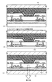
本発明の実施の形態について図1、2を用いて説明する。なお、図1、2に示したのは画素部における作製工程を示す断面図である。また、本実施の形態によって作製される画素の上面図を図3に示す。図3に用いた符号は図1、2で用いた符号に対応している。
【0013】
図1(A)において、101は素子が形成される基板(以下、素子形成基板という)であり、その上には非晶質シリコン膜からなる剥離層102が100〜500nm(本実施の形態では300nm)の厚さに形成される。本実施の形態では素子形成基板101としてガラス基板を用いるが、石英基板、シリコン基板、金属基板もしくはセラミックス基板を用いても構わない。
【0014】
なお、本明細書中では、半導体素子もしくは発光素子が形成された基板全体を指して素子形成基板と呼ぶ場合もある。
【0015】
また、剥離層102の成膜は減圧熱CVD法、プラズマCVD法、スパッタ法もしくは蒸着法を用いれば良い。剥離層102の上には酸化シリコン膜からなる絶縁膜103が200nmの厚さに形成される。絶縁膜103の形成は減圧熱CVD法、プラズマCVD法、スパッタ法もしくは蒸着法を用いれば良い。
【0016】
また、絶縁膜103の上には結晶質シリコン膜104が50nmの厚さに形成される。結晶質シリコン膜104の形成方法としては公知の手段を用いることが可能である。固体レーザーもしくはエキシマレーザーを用いて非晶質シリコン膜をレーザー結晶化させても良いし、非晶質シリコン膜を加熱処理(ファーネスアニール)により結晶化させても良い。
【0017】
次に、図1(B)に示すように、結晶質シリコン膜104をパターニングして島状の結晶質シリコン膜(以下、活性層という)105、106を形成する。そして活性層を覆って酸化シリコン膜からなるゲート絶縁膜107を80nmの厚さに形成する。さらに、ゲート絶縁膜107の上にゲート電極108、109を形成する。本実施の形態ではゲート電極108、109の材料として、350nm厚のタングステン膜もしくはタングステン合金膜を用いる。勿論、ゲート電極の材料としては他の公知の材料を用いることができる。
【0018】
そして、ゲート電極108、109をマスクとして周期表の13族に属する元素(代表的にはボロン)を添加する。添加方法は公知の手段を用いれば良い。こうしてp型の導電型を示す不純物領域(以下、p型不純物領域という)110〜114が形成される。また、ゲート電極の直下にはチャネル形成領域115〜117が画定する。なお、p型不純物領域110〜114はTFTのソース領域もしくはドレイン領域となる。
【0019】
次に、図1(C)に示すように、保護膜(ここでは窒化シリコン膜)118を50nmの厚さに形成し、その後、加熱処理を行って添加された周期表の13族に属する元素の活性化を行う。この活性化はファーネスアニール、レーザーアニールもしくはランプアニールにより行うか、又はそれらを組み合わせて行えば良い。本実施の形態では500℃4時間の加熱処理を窒素雰囲気で行う。
【0020】
活性化が終了したら、水素化処理を行うと効果的である。水素化処理は公知の水素アニール技術もしくはプラズマ水素化技術を用いれば良い。
【0021】
次に、図1(D)に示すように、酸化シリコン膜からなる第1層間絶縁膜119を800nmの厚さに形成し、コンタクトホールを形成して配線120〜123を形成する。第1層間絶縁膜119としては他の無機絶縁膜を用いても良いし、樹脂(有機絶縁膜)を用いても良い。本実施の形態では配線120〜123としてチタン/アルミニウム/チタンの三層構造からなる金属配線を用いる。勿論、導電膜であれば如何なる材料を用いても良い。配線120〜123はTFTのソース配線もしくはドレイン配線となる。
【0022】
この状態でスイッチング用TFT201及び電流制御用TFT(駆動用TFT)202が完成する。本実施の形態ではどちらのTFTもpチャネル型TFTで形成される。但し、スイッチング用TFT201はゲート電極が活性層を二カ所で横切るように形成されており、二つのチャネル形成領域が直列に接続された構造となっている。このような構造とすることでオフ電流値(TFTがオフされた時に流れる電流)を効果的に抑制することができる。
【0023】
また、同時に図3(B)に示すように保持容量301が形成される。保持容量301はTFTの活性層と同時に形成された半導体層302、ゲート絶縁膜107及びゲート電極109で形成される下側保持容量と、ゲート電極109、第1層間絶縁膜119及び配線123で形成される上側保持容量とで形成される。また、半導体層302は配線123と電気的に接続されている。
【0024】
次に、図1(E)に示すように、金属膜を100nmの厚さに形成し、パターニングにより画素電極(EL素子の陽極として機能する)124を形成する。このとき、配線122と画素電極124とはオーミック接触をする。従って、画素電極124と電流制御用TFT202とは電気的に接続される。なお、金属膜としては、白金(Pt)、クロム(Cr)、タングステン(W)もしくはニッケル(Ni)を用いることができる。また、半導体膜としては、シリコン(Si)もしくはゲルマニウム(Ge)を用いることができる。
【0025】
また、ここで形成された画素電極124を上面から見ると図3(A)に示すような構造となっている。但し、図3(A)に示す上面図では有機EL材料および陰極を図示していない。
【0026】
図3(A)に示すように、画素電極124は複数のスリット300を有し、電流制御TFT202のドレイン配線122に接続される。また、画素電極124はスイッチングTFT201および電流制御TFT202のチャネル形成領域を隠す遮光膜としても機能している。また、本実施の形態では、スリット300の間隔(図3(A)中のAで示される距離)を2μm、スリットの幅(図3(A)中のBで示される距離)を20μmとする。
【0027】
画素電極124を形成したら、酸化シリコン膜からなる第2層間絶縁膜125を300nmの厚さに形成する。そして、開口部126を形成し、1〜20nm(好ましくは3〜5nm)の厚さの無機材料からなる絶縁膜を形成する。この様子を図4に示す。図4(A)において401で示された領域を拡大したのが図4(B)である。図4(B)に示すように画素電極124を覆うように無機材料からなる絶縁膜402が形成されている。
【0028】
無機材料からなる絶縁膜402としては、珪素を含む絶縁膜(典型的には酸化珪素膜、窒化珪素膜、窒化酸化珪素膜もしくはこれらにアルミニウムを添加した膜)、酸化タンタル膜、酸化アルミニウムまたは非晶質炭素膜(ダイヤモンドライクカーボン膜を含む)を用いることができる。膜厚はトンネル電流が流れる程度に薄いことが望ましく、1〜20nm(好ましくは3〜5nm)とする。
【0029】
図4(B)のような構造とすると、有機EL層127が直接第1層間絶縁膜119に触れることがない。第1層間絶縁膜119として樹脂膜を用いるような場合には有効な構造である。もちろん、無機材料からなる絶縁膜402は省略することも可能である。
【0030】
次に、70nm厚の有機EL層127及び300nm厚の陰極128を蒸着法により形成する。なお、陰極128としては、MgAg(マグネシウムと銀の合金)膜とアルミニウム膜との積層膜またはリチウムを含有したアルミニウム膜を用いることができる。
【0031】
また、本実施の形態では有機EL層127として20nm厚の正孔注入層及び50nm厚の発光層を積層した構造を用いる。勿論、発光層に正孔注入層、正孔輸送層、電子輸送層もしくは電子注入を組み合わせた公知の他の構造を用いても良い。
【0032】
本実施の形態では、正孔注入層としてCuPc(銅フタロシアニン)を用いる。この場合、まず全ての画素電極を覆うように銅フタロシアニンを形成し、その後、赤色、緑色及び青色に対応する画素ごとに各々赤色の発光層、緑色の発光層及び青色の発光層を形成する。形成する領域の区別は蒸着時にシャドーマスクを用いて行えば良い。このようにすることでカラー表示が可能となる。
【0033】
なお、緑色の発光層を形成する時は、発光層の母体材料としてAlq3(トリス−8−キノリノラトアルミニウム錯体)を用い、キナクリドンもしくはクマリン6をドーパントとして添加する。また、赤色の発光層を形成する時は、発光層の母体材料としてAlq3を用い、DCJT、DCM1もしくはDCM2をドーパントとして添加する。また、青色の発光層を形成する時は、発光層の母体材料としてBAlq3(2−メチル−8−キノリノールとフェノール誘導体の混合配位子を持つ5配位の錯体)を用い、ペリレンをドーパントとして添加する。
【0034】
また、陽極とEL層との間に導電性ポリマーを設けても良い。可溶性の導電性ポリマーを印刷法もしくはインクジェット法で塗布すると、画素電極124のスリット300による段差を平坦化するという効果が得られる。
【0035】
勿論、本願発明では上記有機材料に限定する必要はなく、公知の低分子系有機EL材料、高分子系有機EL材料もしくは無機EL材料を用いることが可能である。高分子系有機EL材料を用いる場合は塗布法を用いることもできる。
【0036】
以上のようにして、画素電極(陽極)124、無機材料からなる絶縁膜402、有機EL層127及び陰極128からなるEL素子(図3(B)において303で示される)が形成される。本実施の形態ではこのEL素子が発光素子として機能する。
【0037】
次に、図2(A)に示すように、第1接着剤129により素子を固定するための基板(以下、固定基板という)130を貼り合わせる。本実施の形態では固定基板130として可撓性のプラスチックフィルムを用いるが、ガラス基板、石英基板、プラスチック基板、シリコン基板もしくはセラミックス基板を用いても良い。なお、プラスチックフィルムとしては、PES(ポリエチレンサルファイル)、PC(ポリカーボネート)、PET(ポリエチレンテレフタレート)もしくはPEN(ポリエチレンナフタレート)を用いることができる。
【0038】
また、第1接着剤129としては、後に剥離層102を除去する際に選択比のとれる材料を用いる必要がある。代表的には樹脂からなる絶縁膜を用いることができ、本実施の形態ではポリイミドを用いるが、アクリル、ポリアミドもしくはエポキシ樹脂を用いても良い。なお、EL素子から見て観測者側(発光装置の使用者側)に位置する場合は、光を透過する材料であることが必要である。
【0039】
図2(A)のプロセスを行うことによりEL素子を完全に大気から遮断することができる。これにより酸化による有機EL材料の劣化をほぼ完全に抑制することができ、EL素子の信頼性を大幅に向上させることができる。
【0040】
次に、図2(B)に示すように、EL素子の形成された基板全体を、フッ化ハロゲンを含むガス中に晒し、剥離層102の除去を行う。なお、フッ化ハロゲンとは化学式XFn(Xはフッ素以外のハロゲン、nは整数)で示される物質であり、一フッ化塩素(ClF)、三フッ化塩素(ClF3)、一フッ化臭素(BrF)、三フッ化臭素(BrF3)、一フッ化ヨウ素(IF)もしくは三フッ化ヨウ素(IF3)を用いることができる。
【0041】
本実施の形態ではフッ化ハロゲンとして三フッ化塩素(ClF3)を用い、希釈ガスとして窒素を用いる。希釈ガスとしては、アルゴン、ヘリウムもしくはネオンを用いても良い。流量は共に500sccm(8.35×10⁻⁶m3/s)とし、反応圧力は1〜10Torr(1.3×102〜1.3×103Pa)とすれば良い。また、処理温度は室温(典型的には20〜27℃)で良い。
【0042】
この場合、シリコン膜はエッチングされるが、プラスチックフィルム、ガラス基板、ポリイミド膜、酸化シリコン膜はエッチングされない。即ち、三フッ化塩素ガスに晒すことで剥離層102が選択的にエッチングされ、最終的には完全に除去される。なお、同じくシリコン膜で形成されている活性層105、106はゲート絶縁膜107に覆われているため三フッ化塩素ガスに晒されることがなく、エッチングされることはない。
【0043】
本実施の形態の場合、剥離層102は露呈した端部から徐々にエッチングされていき、完全に除去された時点で素子形成基板101と絶縁膜103が分離される。このとき、TFT及びEL素子は薄膜を積層して形成されているが、固定基板130に移された形で残る。
【0044】
なお、ここでは剥離層102が端部からエッチングされていくことになるが、素子形成基板101が大きくなると完全に除去されるまでの時間が長くなり好ましいものではない。従って、本実施の形態は素子形成基板101が対角3インチ以下(好ましくは対角1インチ以下)の場合に実施することが望ましい。
【0045】
こうして固定基板130にTFT及びEL素子を移したら、図2(C)に示すように、第2接着剤131を形成し、プラスチックフィルム132を貼り合わせる。第2接着剤131としては樹脂からなる絶縁膜(代表的にはポリイミド、アクリル、ポリアミドもしくはエポキシ樹脂)を用いても良いし、無機材料からなる絶縁膜(代表的には酸化シリコン膜)を用いても良い。なお、EL素子から見て観測者側に位置する場合は、光を透過する材料であることが必要である。
【0046】
こうしてガラス基板101からプラスチックフィルム132へとTFT及びEL素子が移される。その結果、二枚のプラスチックフィルム130、132によって挟まれたフレキシブルなEL表示装置を得ることができる。このように固定基板(ここではプラスチックフィルム)130と貼り合わせ基板(ここではプラスチックフィルム)132を同一材料とすると熱膨張係数が等しくなるので、温度変化による応力歪みの影響を受けにくくすることができる。
【0047】
以上のような本発明の発光装置は、EL素子の陽極として金属膜もしくは半導体膜を用いることができるため、ゴミの発生等の成膜時の不具合を従来の酸化物導電膜よりも低減しうる。そのため、作製工程における歩留まりが向上し、製造コストの低減を図ることができる。
【0048】
さらに本実施の形態により作製されたEL表示装置は、フォトリソグラフィに必要なマスク枚数がトータルで6枚と非常に少なく、高い歩留まりと低い製造コストを達成することができる。また、こうして形成されたEL表示装置は、プラスチック支持体の耐熱性に制限されることなく形成されたTFTを半導体素子として用いることができるので非常に高性能なものとすることができる。
【0049】
なお、本発明の構成は、本実施の形態の構成に限定されるべきものではない。
本発明は陰極もしくは陽極にスリットが設けられている点に特徴があり、その他の構成は如何なる構成であっても良い。例えば、アクティブマトリクス型の表示装置に限らず、パッシブマトリクス型の表示装置に適用することもできる。
【0050】
【実施例】
〔実施例1〕
本実施例では、図1〜図3とは異なる構造の画素部を有する発光装置について説明する。説明には図5、図6を用いる。
【0051】
まず、図1の作製工程に従って図1(D)の工程まで行う。但し、本実施例では画素電極501を、スリットを設けずに形成する。また、本実施例では画素電極501の形成材料として白金を用いる。(図5(A))
【0052】
次に、発明の実施の形態で説明したように、同様に第2層間絶縁膜125を形成し、開口部126を形成して有機EL層502を形成する。EL層502の形成は実施例1に従えば良い。また、EL層502の上に陰極503を形成する。本実施例では陰極503の材料としてリチウムを添加したアルミニウム膜を用いる。なお、陰極503の成膜は蒸着法を用いるが、本実施例ではシャドーマスクを用いることによりスリットを有した陰極とする。ここで図5(B)の状態の上面図を図6に示す。
【0053】
図6において、503が陰極であり、陰極503には複数のスリット504が設けられている。この場合、スリット504の部分だけ陰極503の下に形成されたEL層が露呈することになる。そこで本実施例では図5(C)に示すように陰極503を覆うパッシベーション膜505を形成する。
【0054】
パッシベーション膜505としては、無機材料からなる絶縁膜を用いることができる。本実施例では300nmの厚さの窒化珪素膜を用い、有機EL層502が外気に触れることを防ぐ構造となっている。このパッシベーション膜505は陰極503を形成した後に大気解放しないで連続的に形成することが望ましい。
【0055】
このあとは、発明の実施の形態で説明したように、第1接着剤129により固定基板130を貼り合わせ、EL素子の形成された基板全体を、フッ化ハロゲンを含むガス中に晒して剥離層102の除去を行う。本実施例ではフッ化ハロゲンとして三フッ化塩素(ClF3)を用い、希釈ガスとして窒素を用いる。その他の条件は発明の実施の形態を参照すれば良い。
【0056】
そして、固定基板130にTFT及びEL素子を移したら、第2接着剤131によりプラスチックフィルム132を貼り合わせる。こうしてガラス基板101からプラスチックフィルム132へとTFT及びEL素子が移され、図5(C)に示すEL発光装置が得られる。
【0057】
〔実施例2〕
本発明において、固定基板及び/又は貼り合わせ基板の片面もしくは両面にDLC(ダイヤモンドライクカーボン)膜を形成しておくことは有効である。但し、膜厚が厚すぎると透過率が落ちるので、50nm以下(好ましくは10〜20nm)とすると良い。
【0058】
DLC膜の特徴としては、1550cm-1くらいに非対称のピークを有し、1300cm-1くらいに肩をもつラマンスペクトル分布を有する。また、微小硬度計で測定した時に15〜25Paの硬度を示すという特徴をもつ。
【0059】
DLC膜はプラスチック支持体に比べて硬度が大きく、熱伝導率も大きいため、表面保護や熱分散のための保護膜として設けておくことが有効である。
【0060】
従って、プラスチック支持体を貼り付ける前に予めDLC膜を成膜しておいて貼り付けるか、プラスチック支持体を貼り付けた後にDLC膜を成膜することも可能である。いずれにしてもDLC膜の成膜はスパッタ法もしくはECRプラズマCVD法を用いれば良い。
【0061】
〔実施例3〕
本発明のEL発光装置は図7に示す回路構成の画素部とすることができる。図7において、701はソース配線、702はゲート配線、703はスイッチングTFT、704は電流制御TFT、705は電流供給線、706はEL素子である。本実施例ではスイッチングTFT703および電流制御TFT704がpチャネル型TFTで作製されている。勿論、スイッチングTFT703および電流制御TFT704はどちらか片方がnチャネル型TFTであっても良いし、両者がnチャネル型TFTであっても良い。
【0062】
なお、本実施例では図3のコンデンサ301と同じ役割を、電流制御TFT704のゲート容量で補っている。これは、デジタル駆動により時分割階調表示を行う場合、1フレーム期間(もしくは1フィールド期間)が短いため、電流制御TFTのゲート容量だけで電荷を保持しうるためである。
【0063】
なお、本実施例の構成は実施例1、2の構成と組み合わせて実施することが可能である。
【0064】
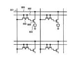
〔実施例4〕
実施例3において、図7に示した画素部の回路構成は、図8に示した回路構成としても良い。図8において、801はソース配線、802はゲート配線、803はスイッチングTFT、804は電流制御TFT、805は電流供給線、806はEL素子である。本実施例ではスイッチングTFT803および電流制御TFT804がpチャネル型TFTで作製されている。勿論、スイッチングTFT703および電流制御TFT704はどちらか片方がnチャネル型TFTであっても良いし、両者がnチャネル型TFTであっても良い。
【0065】
このとき、ゲート配線802と電流供給線805は異なる層に形成されるため、両者が層間絶縁膜を挟んで重なるように設けることは有効である。このようにすることで実質的に配線の占有面積を共通化することができ、画素の有効発光面積を増やすことができる。
【0066】
なお、本実施例の構成は実施例1〜3のいずれの構成とも自由に組み合わせて実施することが可能である。
【0067】
〔実施例5〕
本実施例では、本発明のEL発光装置の外観図を説明する。なお、図9(A)は本発明のEL発光装置の上面図であり、図9(B)はその断面図である。
【0068】
図9(A)において、901は素子形成基板、902は画素部、903はソース側駆動回路、904はゲート側駆動回路であり、それぞれの駆動回路は配線905を経てFPC(フレキシブルプリントサーキット)906に至り、外部機器へと接続される。このとき、画素部902、ソース側駆動回路903及びゲート側駆動回路904を囲むようにして第1シール材911、カバー材912、接着剤913(図9(B)参照)及び第2シール材914が設けられている。
【0069】
また、図9(B)は図9(A)をA−A’で切断した断面図に相当する。このとき、素子形成基板901の上方(厳密には素子形成基板901上に設けられた絶縁体の上)には駆動回路を形成するTFT91、スイッチングTFT92および電流制御TFT93が設けられる。スイッチングTFT92および電流制御TFT93の形成方法は既に説明したので省略する。本実施例では電流制御TFT93の画素電極(陽極)にスリットが設けられている。また、駆動回路を形成するTFT93は、公知のCMOS回路、PMOS回路もしくはNMOS回路で形成すれば良い。
【0070】
EL素子の陰極は915で示される領域において配線905に電気的に接続される。配線905は陰極に所定の電圧を与えるための配線であり、異方導電性フィルム916を介してFPC906に電気的に接続される。さらにEL素子は、第1シール材911及びそれによって基板901に貼り合わされたカバー材912で囲まれ、接着剤913により封入されている。
【0071】
なお、接着剤913の中にスペーサを含有させてもよい。このとき、スペーサを酸化バリウムで形成すればスペーサ自体に吸湿性をもたせることが可能である。また、スペーサを設けた場合、スペーサからの圧力を緩和するバッファ層として陰極上に樹脂膜を設けることも有効である。
【0072】
また、接着剤913の代わりに不活性ガス(希ガスもしくは窒素ガス)を封入することもできる。この際、加圧雰囲気で不活性ガスの封入工程を行えば、外部からの酸素や水の侵入を効果的に防ぐことが可能である。
【0073】
また、配線905は異方導電性フィルム916を介してFPC906に電気的に接続される。配線905は画素部902、ソース側駆動回路903及びゲート側駆動回路904に送られる信号をFPC906に伝え、FPC906により外部機器と電気的に接続される。
【0074】
また、本実施例では第1シール材911の露呈部及びFPC906の一部を覆うように第2シール材914を設け、EL素子を徹底的に外気から遮断する構造となっている。こうして図9(B)の断面構造を有するEL発光装置となる。なお、本実施例のEL発光装置は実施例1〜4のいずれの構成を組み合わせて作製しても構わない。
【0075】
〔実施例6〕
本実施例では、本発明のEL発光装置の画素構造について図10(A)、(B)に示す。本実施例において、1001はスイッチングTFT1002のソース配線、1003はスイッチングTFT1002のゲート配線、1004は電流制御TFT、1005はコンデンサ(省略することも可能)、1006は電流供給線、1007は電源制御TFT、1008はEL素子、1009は電源制御線とする。このとき、ソース配線1001、ゲート配線1003、電流供給線1006および電源制御線1009が同一の層に同一の導電膜で形成される。
【0076】
なお、電源制御TFT1007の動作については特願平11−341272号を参照すると良い。ただし本実施例では電源制御TFTを電流制御TFTと同一構造のpチャネル型TFTとする。
【0077】
また、本実施例では電源制御TFT1007を電流制御TFT1004とEL素子1008との間に設けているが、電源制御TFT1007とEL素子1008との間に電流制御TFT1004が設けられた構造としても良い。また、電源制御TFT1007は電流制御TFT1004と同一構造とするか、同一の活性層で直列させて形成するのが好ましい。
【0078】
また、図10(A)は、二つの画素間で電流供給線1006を共通とした場合の例である。即ち、二つの画素が電流供給線1006を中心に線対称となるように形成されている点に特徴がある。この場合、電流供給線の本数を減らすことができるため、画素部をさらに高精細化することができる。また、図10(B)は、ゲート配線1003と平行に電流供給線1010を設け、ソース配線1001と平行に電源制御線1011を設けた場合の例である。
【0079】
なお、本実施例の構成は実施例1〜5のいずれの構成とも自由に組み合わせて実施することが可能である。
【0080】
〔実施例7〕
本実施例では、本発明のEL発光装置の画素構造について図11(A)、(B)に示す。なお、本実施例において、1101はスイッチングTFT1102のソース配線、1103はスイッチングTFT1102のゲート配線、1104は電流制御TFT、1105はコンデンサ(省略することも可能)、1106は電流供給線、1107は消去TFT、1108は消去用ゲート配線、1109はEL素子とする。このとき、ソース配線1101、ゲート配線1103、電流供給線1106および消去用ゲート配線1108が同一の層に同一の導電膜で形成される。
【0081】
なお、消去TFT1107の動作については特願平11−338786号を参照すると良い。ただし本実施例では電源制御TFTを電流制御TFTと同一構造のpチャネル型TFTとする。また、特願平11−338786号では消去用ゲート配線を消去用ゲート信号線と呼んでいる。
【0082】
消去TFT1107のドレインは電流制御TFT1104のゲートに接続され、電流制御TFT1104のゲート電圧を強制的に変化させることができるようになっている。なお、消去TFT1107はpチャネル型TFTとし、オフ電流を小さくできるようにスイッチング用TFT1102と同一構造とすることが好ましい。
【0083】
また、図11(A)は、二つの画素間で電流供給線1106を共通とした場合の例である。即ち、二つの画素が電流供給線1106を中心に線対称となるように形成されている点に特徴がある。この場合、電流供給線の本数を減らすことができるため、画素部をさらに高精細化することができる。また、図11(B)は、ゲート配線1103と平行に電流供給線1110を設け、ソース配線1101と平行に消去ゲート配線1111を設けた場合の例である。
【0084】
なお、本実施例の構成は実施例1〜5のいずれの構成とも自由に組み合わせて実施することが可能である。
【0085】
〔実施例8〕
本発明のEL発光装置は画素内にいくつのTFTを設けた構造としても良い。
実施例6、7ではTFTを三つ設けた例を示しているが、四つ乃至六つのTFTを設けても構わない。本発明はEL発光装置の画素構造に限定されずに実施することが可能である。
【0086】
なお、本実施例の構成は実施例1〜5のいずれの構成とも自由に組み合わせて実施することが可能である。
【0087】
〔実施例9〕
「発明の実施の形態」において、絶縁膜103に窒化珪素膜もしくは窒化酸化珪素膜を設け、保護膜118に窒化珪素膜もしくは窒化酸化珪素膜を設ける構成とすることが好ましい。
【0088】
このような構造とすると、スイッチング用TFT201および電流制御用TFT202が窒化珪素膜もしくは窒化酸化珪素膜で挟まれた構造となり、外部からの水分や可動イオンの侵入を効果的に防ぐことができる。
【0089】
また、第1層間絶縁膜119として有機絶縁膜を用いる場合、第1層間絶縁膜119と画素電極124の間に窒化珪素膜もしくはDLC(ダイヤモンドライクカーボン)膜を設け、さらに陰極128の上に前述の窒化珪素膜もしくはDLC膜を設けることは好ましい。
【0090】
このような構造とすると、EL素子303が窒化珪素膜もしくはDLC膜で挟まれた構造となり、外部からの水分や可動イオンの侵入を防ぐだけでなく、酸素の侵入をも効果的に防ぐことができる。EL素子中の発光層などの有機材料は酸素によって容易に酸化して劣化するため、本実施例のような構造とすることで大幅に信頼性を向上することができる。
【0091】
以上のように、TFTを保護するための対策とEL素子を保護するための対策を併用して施すことで電子装置全体の信頼性を高めることができる。
【0092】
なお、本実施例の構成は、実施例1〜実施例8のいずれの構成とも自由に組み合わせることが可能である。
【0093】
〔実施例10〕
本実施例では、スリットを設けた画素電極の上に導電性ポリマー膜を形成した例を図15に示す。なお、本実施例の発光装置は、EL層の構成以外の構成にお
いて
【発明の実施の形態】
に示した発光装置と同じである。従って、EL層の構成以外の説明は省略する。
【0094】
導電性ポリマーとしては、共役系高分子であるポリアセチレン、ポリチオフェン、ポリ(3−メチル)チオフェン、ポリ(3−エチル)チオフェン、ポリ(3−n−ブチル)チオフェン、ポリ(3−ヘキシル)チオフェン、ポリ(3−オクチル)チオフェン、ポリ(3−ドデシル)チオフェン、ポリ(3−オクタデシル)チオフェン、ポリ(3−アイコシル)チオフェンもしくはポリ(3−メチル−Co−ブチル)チオフェンに、ドーパントとしてPF6 -、臭素もしくはヨウ素を用いたものを用いることができる。
【0095】
なお、ポリ(3−ヘキシル)チオフェン、ポリ(3−オクチル)チオフェン、ポリ(3−ドデシル)チオフェン、ポリ(3−オクタデシル)チオフェン、ポリ(3−アイコシル)チオフェン及びポリ(3−メチル−Co−ブチル)チオフェンは可溶性である。溶媒としては、クロロホルム、ベンゼンもしくはテトラリンなどを用いることができる。
【0096】
本実施例では、スリット300を設けた画素電極(陽極)124上に導電性ポリマー膜150を10〜50nm(好ましくは20〜30nm)の厚さに形成する。導電性ポリマー膜150として可溶性のものを用い、印刷法もしくはインクジェット法により成膜すればスリット300による段差を平坦化することが可能である。
【0097】
そして、導電性ポリマー膜150上に、発光層151としてAlq3を蒸着法により形成する。勿論、公知の発光層で代用しても良い。
【0098】
こうしてEL層が形成されたら、その上に陰極128としてリチウムを含有したアルミニウム膜を形成する。
【0099】
以上のようにして、画素電極124、導電性ポリマー膜150、発光層151および陰極128からなるEL素子152が形成される。
【0100】
なお、本実施例の構成は、実施例1〜9のいずれの構成とも組み合わせて実施することが可能である。
【0101】
〔実施例11〕
本実施例ではEL層および陰極を形成するための成膜装置について図12を用いて説明する。図12において、1201は搬送室(A)であり、搬送室(A)1201には搬送機構(A)1202が備えられ、基板1203の搬送が行われる。搬送室(A)1201は減圧雰囲気にされており、各処理室とはゲートによって遮断されている。各処理室への基板の受け渡しは、ゲートを開けた際に搬送機構(A)によって行われる。
【0102】
また、搬送室(A)1201を減圧するためにクライオポンプを用いる。なお、図12の成膜装置では、搬送室(A)1201の側面に排気ポート1204が設けられ、その下に排気ポンプが設置される。このような構造とすると排気ポンプのメンテナンスが容易になるという利点がある。
【0103】
以下に、各処理室についての説明を行う。なお、搬送室(A)1201は減圧雰囲気となるので、搬送室(A)1201に直接的に連結された処理室には全て排気ポンプ(図示せず)が備えられている。排気ポンプとしては油回転ポンプ、メカニカルブースターポンプ、ターボ分子ポンプもしくはクライオポンプが用いられる。
【0104】
まず、1205は基板のセッティング(設置)を行うストック室であり、ロードロック室とも呼ばれる。ストック室1205はゲート1200aにより搬送室(A)1201と遮断され、ここに基板1203をセットしたキャリア(図示せず)が配置される。また、ストック室1205は上述の排気ポンプと高純度の窒素ガスまたは希ガスを導入するためのパージラインを備えている。
【0105】
また、本実施例では基板1203を、素子形成面を下向きにしてキャリアにセットする。これは後に蒸着法による成膜を行う際に、フェイスダウン方式を行いやすくするためである。フェイスダウン方式とは、基板の素子形成面が下を向いた状態で成膜する方式をいい、この方式によればゴミの付着などを抑えることができる。
【0106】
次に、1206は搬送室(B)であり、ストック室1205とはゲート1200bを介して連結され、搬送機構(B)1207を備えている。また、1208は焼成室(ベーク室)であり、ゲート1200cを介して搬送室(B)1206と連結している。
【0107】
なお、焼成室1208は基板の面の上下を反転させる機構を有する。即ち、フェイスダウン方式で搬送されてきた基板はここで一旦フェイスアップ方式に切り替わる。これは次のスピンコータ室1209での処理がフェイスアップ方式で行えるようにするためである。また逆に、スピンコータ室1209で処理を終えた基板は再び焼成室1208に戻ってきて焼成され、再び上下を反転させてフェイスダウン方式に切り替わり、ストック室1205へ戻る。
【0108】
ところでスピンコータ室1209はゲート1200dを介して搬送室(B)1206と連結している。スピンコータ室1209はEL材料を含む溶液を基板上に塗布することでEL材料を含む膜を形成する成膜室であり、主に高分子系(ポリマー系)有機EL材料を成膜する。このとき、成膜室は常に窒素やアルゴンなどの不活性ガスで充填しておく。
【0109】
なお、成膜されるEL材料は、発光層として用いるものだけでなく、電荷注入層または電荷輸送層をも含む。また、公知の如何なる高分子系有機EL材料を用いても良い。発光層となる代表的な有機EL材料としては、PPV(ポリパラフェニレンビニレン)誘導体、PVK(ポリビニルカルバゾール)誘導体またはポリフルオレン誘導体が挙げられる。これはπ共役ポリマーとも呼ばれる。また、電荷注入層としては、PEDOT(ポリチオフェン)またはPAni(ポリアニリン)が挙げられる。
【0110】
次に、1210で示されるのはEL素子の画素電極となる陰極もしくは陽極の表面を処理する処理室(以下、前処理室という)であり、前処理室1210はゲート1200eにより搬送室(A)1201と遮断される。前処理室はEL素子の作製プロセスによって様々に変えることができるが、ここでは画素電極の表面に紫外光を照射しつつ100〜120℃で加熱できるようにする。このような前処理は、EL素子の陽極表面を処理する際に有効である。
【0111】
次に、1211は蒸着法により導電膜またはEL材料を形成するための蒸着室であり、ゲート1200fを介して搬送室(A)1201に連結される。蒸着室1211は内部に複数の蒸着源を設置できる。また、抵抗加熱または電子ビームにより蒸着源を蒸発させ、成膜を行うことができる。
【0112】
この蒸着室1211で形成される導電膜はEL素子の陰極側の電極として設けられる導電膜であり、仕事関数の小さい金属、代表的には周期表の1族もしくは2族に属する元素(代表的にはリチウム、マグネシウム、セシウム、カルシウム、カリウム、バリウム、ナトリウムもしくはベリリウム)またはそれらに近い仕事関数をもつ金属を蒸着できる。また、低抵抗な導電膜としてアルミニウム、銅もしくは銀を蒸着することもできる。さらに、透明導電膜として酸化インジウムと酸化スズとの化合物からなる導電膜や酸化インジウムと酸化亜鉛との化合物からなる導電膜を蒸着法により形成することも可能である。
【0113】
また、蒸着室1211では公知のあらゆるEL材料(特に低分子系有機EL材料)を形成することが可能である。発光層の代表例としてはAlq3(トリス−8−キノリノラトアルミニウム錯体)もしくはDSA(ジスチルアリーレン誘導体)があり、電荷注入層の代表例としてはCuPc(銅フタロシアニン)、LiF(フッ化リチウム)もしくはacacK(カリウムアセチルアセトネート)があり、電荷輸送層の代表例としてはTPD(トリフェニルアミン誘導体)もしくはNPD(アントラセン誘導体)が挙げられる。
【0114】
また、上記EL材料と蛍光物質(代表的には、クマリン6、ルブレン、ナイルレッド、DCM、キナクリドン等)とを共蒸着することも可能である。蛍光物質としては公知の如何なる材料を用いても良い。また、EL材料と周期表の1族または2族に属する元素とを共蒸着して発光層の一部に電荷輸送層または電荷注入層としての役割をもたせることも可能である。なお、共蒸着とは、同時に蒸着源を加熱し、成膜段階で異なる物質を混合する蒸着法をいう。
【0115】
いずれにしてもゲート1200fによって搬送室(A)1201と遮断され、真空下でEL材料または導電膜の成膜が行われる。なお、成膜はフェイスダウン方式で行われる。
【0116】
次に、1212は封止室(封入室またはグローブボックスともいう)であり、ゲート1200gを介して搬送室(A)1201に連結されている。封止室1212では、最終的にEL素子を密閉空間に封入するための処理が行われる。この処理は形成されたEL素子を酸素や水分から保護するための処理であり、カバー材で機械的に封入する、又は熱硬化性樹脂若しくは紫外光硬化性樹脂で封入するといった手段を用いる。
【0117】
カバー材と上記EL素子が形成された基板とは熱硬化性樹脂又は紫外光硬化性樹脂を用いて貼り合わせられ、熱処理又は紫外光照射処理によって樹脂を硬化させて密閉空間を形成する。
【0118】
図12に示した成膜装置では、封止室1212の内部に紫外光を照射するための機構(以下、紫外光照射機構という)1213が設けられており、この紫外光照射機構1213から発した紫外光によって紫外光硬化性樹脂を硬化させる構成となっている。封止室1212の内部は排気ポンプを取り付けることで減圧することも可能であるし、高純度な窒素ガスや希ガスでパージしつつ与圧とすることも可能である。
【0119】
次に、封止室1212には受渡室(パスボックス)1214が連結される。受渡室1214には搬送機構(C)1215が設けられ、封止室1212でEL素子の封入が完了した基板を受渡室1214へと搬送する。受渡室1214も排気ポンプを取り付けることで減圧することが可能である。この受渡室1214は封止室1212を直接外気に晒さないようにするための設備であり、ここから基板を取り出す。
【0120】
以上のように、図12に示した成膜装置を用いることで完全にEL素子を密閉空間に封入するまで外気に晒さずに済む。このような成膜装置を用いることで信頼性の高いEL発光装置を作製することが可能となる。
【0121】
〔実施例12〕
本発明は、バックライト等の光源として用いるEL発光装置に対して実施することが可能である。光源として用いる場合、基板上に発光素子を形成すれば良いだけである。
【0122】
本発明は発光素子の陽極もしくは陰極にスリットを設けることで、陽極として金属膜もしくは半導体膜を用いることができる。従って、発光素子の面積に拘わらず本発明を実施することが可能である。
【0123】
〔実施例13〕
本発明を実施して形成したEL発光装置は様々な電気器具の表示部もしくは光源として用いることができる。例えば、TV放送等を鑑賞するには対角20〜60インチの本発明のEL発光装置を筐体に組み込んだディスプレイを用いるとよい。なお、EL発光装置を筐体に組み込んだディスプレイには、パソコン用ディスプレイ、TV放送受信用ディスプレイ、広告表示用ディスプレイ等の全ての情報表示用ディスプレイが含まれる。
【0124】
また、その他の本発明の電気器具としては、ビデオカメラ、デジタルカメラ、ゴーグル型ディスプレイ(ヘッドマウントディスプレイ)、ナビゲーションシステム、音楽再生装置(カーオーディオ、オーディオコンポ等)、ノート型パーソナルコンピュータ、ゲーム機器、携帯情報端末(モバイルコンピュータ、携帯電話、携帯型ゲーム機または電子書籍)、画像再生装置(記録媒体に記録された画像を再生し、その画像を表示する表示部を備えた装置)が挙げられる。それら電気器具の具体例を図13、図14に示す。
【0125】
図13(A)はEL発光装置を筐体に組み込んだディスプレイであり、筐体2001、支持台2002、表示部2003を含む。本発明のEL発光装置は表示部2003に用いることができる。このようなディスプレイは自発光型であるためバックライトが必要なく、液晶ディスプレイよりも薄い表示部とすることができる。
【0126】
図13(B)はビデオカメラであり、本体2101、表示部2102、音声入力部2103、操作スイッチ2104、バッテリー2105、受像部2106を含む。本発明のEL発光装置は表示部2102に用いることができる。
【0127】
図13(C)は頭部取り付け型のELディスプレイの一部(右片側)であり、本体2201、信号ケーブル2202、頭部固定バンド2203、表示部2204、光学系2205、発光装置2206を含む。本発明はEL発光装置2206に用いることができる。
【0128】
図13(D)は記録媒体を備えた画像再生装置(具体的にはDVD再生装置)であり、本体2301、記録媒体(DVD等)2302、操作スイッチ2303、表示部(a)2304、表示部(b)2305を含む。表示部(a)は主として画像情報を表示し、表示部(b)は主として文字情報を表示するが、本発明のEL発光装置はこれら表示部(a)、(b)に用いることができる。なお、記録媒体を備えた画像再生装置には家庭用ゲーム機器なども含まれる。
【0129】
図13(E)は携帯型(モバイル)コンピュータであり、本体2401、カメラ部2402、受像部2403、操作スイッチ2404、表示部2405を含む。本発明のEL発光装置は表示部2405に用いることができる。
【0130】
図13(F)はパーソナルコンピュータであり、本体2501、筐体2502、表示部2503、キーボード2504を含む。本発明のEL発光装置は表示部2503に用いることができる。
【0131】
なお、将来的に発光輝度がさらに高くなれば、出力した画像情報を含む光をレンズや光ファイバー等で拡大投影してフロント型若しくはリア型のプロジェクターに用いることも可能となる。
【0132】
また、発光装置は発光している部分が電力を消費するため、発光部分が極力少なくなるように情報を表示することが望ましい。従って、携帯情報端末、特に携帯電話や音楽再生装置のような文字情報を主とする表示部に発光装置を用いる場合には、非発光部分を背景として文字情報を発光部分で形成するように駆動することが望ましい。
【0133】
ここで図14(A)は携帯電話であり、本体2601、音声出力部2602、音声入力部2603、表示部2604、操作スイッチ2605、アンテナ2606を含む。本発明のEL発光装置は表示部2604に用いることができる。なお、表示部2604は黒色の背景に白色の文字を表示することで携帯電話の消費電力を抑えることができる。
【0134】
また、図14(B)は音楽再生装置、具体的にはカーオーディオであり、本体2701、表示部2702、操作スイッチ2703、2704を含む。本発明のEL発光装置は表示部2702に用いることができる。また、本実施例では車載用のカーオーディオを示すが、携帯型や家庭用の音楽再生装置に用いても良い。
なお、表示部2704は黒色の背景に白色の文字を表示することで消費電力を抑えられる。これは携帯型の音楽再生装置において特に有効である。
【0135】
以上の様に、本発明の適用範囲は極めて広く、あらゆる分野の電気器具に用いることが可能である。また、本実施例の電気器具は実施例1〜12に示したいずれの構成の発光装置を用いても良い。
【0136】
【発明の効果】
発光素子の陽極もしくは陰極にスリットを設けることで、陽極として金属膜もしくは半導体膜を用いることが可能となる。これにより従来用いられていた酸化物導電膜を陽極に用いることなく、発光の取り出しが可能な発光素子を形成することが可能となる。
【0137】
また、酸化物導電膜よりも抵抗の低い材料を陽極として用いることが可能となることから、電流注入効率が高く、応答性に優れた発光装置とすることができる。また、そのような発光装置を表示部として用いた高性能な電気器具を得ることができる。
【図面の簡単な説明】
【図1】 発光装置の作製工程を示す図。
【図2】 発光装置の作製工程を示す図。
【図3】 発光装置の上面構造及び回路構成を示す図。
【図4】 発光装置の断面構造を示す図。
【図5】 発光装置の作製工程を示す図。
【図6】 発光装置の上面構造を示す図。
【図7】 発光装置の回路構成を示す図。
【図8】 発光装置の回路構成を示す図。
【図9】 発光装置の上面構造および断面構造を示す図。
【図10】 発光装置の回路構成を示す図。
【図11】 発光装置の回路構成を示す図。
【図12】 薄膜形成装置の構成を示す図。
【図13】 電気器具の一例を示す図。
【図14】 電気器具の一例を示す図。
【図15】 発光装置の断面構造を示す図。[0001]
BACKGROUND OF THE INVENTION
The present invention relates to a device (hereinafter referred to as a light-emitting device) having an element (hereinafter referred to as a light-emitting device) in which a light-emitting material is sandwiched between electrodes and a manufacturing method thereof. In particular, the present invention relates to a light-emitting device (particularly referred to as an EL light-emitting device) using a light-emitting element (hereinafter referred to as an EL element) using a light-emitting material (hereinafter referred to as an EL material) from which EL (Electro Luminescence) can be obtained as a light-emitting material.
[0002]
Note that EL materials that can be used in the present invention include all luminescent materials that emit light (phosphorescence and / or fluorescence) via singlet excitation, triplet excitation, or both excitations.
[0003]
[Prior art]
In recent years, the development of EL light emitting devices has been advanced. An EL light emitting device has a structure having an EL element having a structure in which an EL material is sandwiched between an anode and a cathode. By applying a voltage between the anode and the cathode and passing a current through the EL material, carriers are recombined to emit light. That is, since the EL light emitting device has a light emitting capability, the backlight used for the liquid crystal display device is unnecessary. Furthermore, it has the advantages of a wide viewing angle, light weight, and low power consumption.
[0004]
A conductive film having a high work function, typically a transparent oxide conductive film, is used as the anode of the EL light emitting device. Since the oxide conductive film transmits visible light, light emitted from the EL layer can be easily extracted, but has a disadvantage that resistance is higher than that of the metal film. When the resistance of the anode is high, there is a problem that not only the efficiency of injecting current into the EL layer is deteriorated but also an element having a slow response is obtained.
[0005]
Moreover, although the oxide conductive film is formed by vapor deposition or sputtering, there are many problems such as dust coming out during film formation. In addition, there is a problem that etching becomes difficult due to crystallization, and this is one of the conductive films that is difficult to handle as compared with a metal film.
[0006]
However, since the cathode of the EL light emitting device is a metal film, there is a problem that light cannot be extracted unless a transparent conductive film is used on the anode side. Therefore, at present, there has been no use other than using an oxide conductive film as the anode material.
[0007]
[Problems to be solved by the invention]
It is an object of the present invention to produce a light-emitting device that has a low work resistance, high current injection efficiency, and excellent responsiveness by using a metal film or semiconductor film having a high work function instead of an oxide conductive film as an anode. And It is another object of the present invention to provide a light emitting device having an element structure necessary for this purpose and an electric appliance using the light emitting device.
[0008]
[Means for Solving the Problems]
In the present invention, since a metal film or a semiconductor film having a high work function is used as the anode, a slit (a slit for preventing light from being blocked) is provided in the anode or cathode of the light emitting element, and the function as the anode or cathode is achieved. And an electrode structure that secures a light passage at the same time. At this time, the slit may be provided in the anode or the cathode. Moreover, you may provide in both an anode and a cathode. In the present invention, a metal film or a semiconductor film can be used as an anode by using an electrode provided with a slit as a light path.
[0009]
Here, the interval between the slits (the distance between adjacent slits) is 0.5 to 3 μm (preferably 1.0 to 2.0 μm), and the width of the slit is preferably 5 to 15 times the interval between the slits. For example, when the slit interval is 1.5 μm, the slit width is desirably 10 to 15 μm. Moreover, it is good to provide so that the ratio which a slit may occupy in an anode may be 70 to 90%.
[0010]
In the EL light emitting device, the role of the anode is to inject holes, and it is required that the material has a higher HOMO level than the EL material. That is, it is desirable that the material has a high work function. A material that satisfies such requirements is not limited to an oxide conductive film, and a metal film or a semiconductor film can also be used. As such a metal film, platinum (Pt), chromium (Cr), tungsten (W), or nickel (Ni) can be used. As the semiconductor film, silicon (Si) or germanium (Ge) can be used.
[0011]
By implementing the present invention in this way, the range of selection of materials that can be used as an anode is increased, and it is possible to obtain a light emitting device with a lower driving voltage or a higher luminance than conventional light emitting devices. Become. In addition, since a metal film or a semiconductor film whose resistance is lower than that of the oxide conductive film can be used as the anode, a light-emitting device with high current injection efficiency and excellent response can be obtained.
[0012]
DETAILED DESCRIPTION OF THE INVENTION
An embodiment of the present invention will be described with reference to FIGS. 1 and 2 are cross-sectional views showing a manufacturing process in the pixel portion. A top view of a pixel manufactured according to this embodiment mode is shown in FIG. The codes used in FIG. 3 correspond to the codes used in FIGS.
[0013]
In FIG. 1A,
[0014]
In this specification, the entire substrate on which a semiconductor element or a light emitting element is formed may be referred to as an element formation substrate.
[0015]
In addition, the
[0016]
On the insulating
[0017]
Next, as shown in FIG. 1B, the
[0018]
Then, an element (typically boron) belonging to Group 13 of the periodic table is added using the
[0019]
Next, as shown in FIG. 1C, a protective film (here, a silicon nitride film) 118 is formed to a thickness of 50 nm, and is then subjected to heat treatment, and added to elements belonging to Group 13 of the periodic table. Activation of. This activation may be performed by furnace annealing, laser annealing or lamp annealing, or a combination thereof. In this embodiment, heat treatment at 500 ° C. for 4 hours is performed in a nitrogen atmosphere.
[0020]
When the activation is completed, it is effective to perform a hydrogenation treatment. For the hydrogenation treatment, a known hydrogen annealing technique or plasma hydrogenation technique may be used.
[0021]
Next, as shown in FIG. 1D, a first
[0022]
In this state, the switching
[0023]
At the same time, a
[0024]
Next, as shown in FIG. 1E, a metal film is formed to a thickness of 100 nm, and a pixel electrode (functioning as an anode of an EL element) 124 is formed by patterning. At this time, the
[0025]
Further, when the
[0026]
As shown in FIG. 3A, the
[0027]
After the
[0028]
As the insulating
[0029]
With the structure as shown in FIG. 4B, the
[0030]
Next, a 70 nm thick
[0031]
In this embodiment, a structure in which a 20 nm thick hole injection layer and a 50 nm thick light emitting layer are stacked is used as the
[0032]
In this embodiment, CuPc (copper phthalocyanine) is used as the hole injection layer. In this case, first, copper phthalocyanine is formed so as to cover all the pixel electrodes, and then a red light emitting layer, a green light emitting layer, and a blue light emitting layer are formed for each pixel corresponding to red, green, and blue. The regions to be formed may be distinguished using a shadow mask during vapor deposition. In this way, color display is possible.
[0033]
When forming a green light emitting layer, Alq is used as the base material of the light emitting layer.Three(Tris-8-quinolinolato aluminum complex) is used and quinacridone or coumarin 6 is added as a dopant. When a red light emitting layer is formed, Alq is used as a base material of the light emitting layer.ThreeAnd DCJT, DCM1 or DCM2 is added as a dopant. When a blue light emitting layer is formed, BAlq is used as a base material of the light emitting layer.Three(5-coordinate complex having a mixed ligand of 2-methyl-8-quinolinol and a phenol derivative) and perylene is added as a dopant.
[0034]
Further, a conductive polymer may be provided between the anode and the EL layer. When a soluble conductive polymer is applied by a printing method or an ink jet method, an effect of flattening a step due to the
[0035]
Of course, in the present invention, it is not necessary to limit to the above organic material, and it is possible to use a known low molecular organic EL material, high molecular organic EL material or inorganic EL material. When using a polymer organic EL material, a coating method can also be used.
[0036]
As described above, an EL element (denoted by 303 in FIG. 3B) including the pixel electrode (anode) 124, the insulating
[0037]
Next, as shown in FIG. 2A, a substrate (hereinafter, referred to as a fixed substrate) 130 for fixing the element with a
[0038]
In addition, as the
[0039]
By performing the process of FIG. 2A, the EL element can be completely shielded from the atmosphere. Thereby, deterioration of the organic EL material due to oxidation can be suppressed almost completely, and the reliability of the EL element can be greatly improved.
[0040]
Next, as illustrated in FIG. 2B, the entire substrate on which the EL element is formed is exposed to a gas containing halogen fluoride, and the
[0041]
In this embodiment, chlorine trifluoride (ClF) is used as halogen fluoride.Three) And nitrogen as the diluent gas. Argon, helium, or neon may be used as the dilution gas. Both flow rates were 500 sccm (8.35 × 10⁻⁶mThree/ S), and the reaction pressure is 1 to 10 Torr (1.3 × 10 6).2~ 1.3 × 10ThreePa). The processing temperature may be room temperature (typically 20 to 27 ° C.).
[0042]
In this case, the silicon film is etched, but the plastic film, glass substrate, polyimide film, and silicon oxide film are not etched. That is, the
[0043]
In the case of this embodiment mode, the
[0044]
Note that the
[0045]
When the TFT and the EL element are transferred to the fixed
[0046]
Thus, the TFT and the EL element are transferred from the
[0047]
Since the light emitting device of the present invention as described above can use a metal film or a semiconductor film as an anode of an EL element, it can reduce defects during film formation such as generation of dust as compared with a conventional oxide conductive film. . Therefore, the yield in the manufacturing process can be improved and the manufacturing cost can be reduced.
[0048]
Further, the EL display device manufactured according to this embodiment has a very small number of masks necessary for photolithography, which is 6 in total, and can achieve a high yield and a low manufacturing cost. In addition, the EL display device thus formed can have a very high performance because a TFT formed without being limited by the heat resistance of the plastic support can be used as a semiconductor element.
[0049]
Note that the configuration of the present invention should not be limited to the configuration of the present embodiment.
The present invention is characterized in that a slit is provided in a cathode or an anode, and any other configuration may be used. For example, the invention can be applied not only to an active matrix display device but also to a passive matrix display device.
[0050]
【Example】
[Example 1]
In this embodiment, a light-emitting device having a pixel portion having a structure different from those in FIGS. 5 and 6 are used for the description.
[0051]
First, the steps up to the step of FIG. However, in this embodiment, the
[0052]
Next, as described in the embodiment of the invention, the second
[0053]
In FIG. 6,
[0054]
As the
[0055]
Thereafter, as described in the embodiment of the invention, the fixed
[0056]
Then, after the TFT and the EL element are transferred to the fixed
[0057]
[Example 2]
In the present invention, it is effective to form a DLC (diamond-like carbon) film on one or both surfaces of the fixed substrate and / or the bonded substrate. However, if the film thickness is too thick, the transmittance decreases, so it is preferable to set the thickness to 50 nm or less (preferably 10 to 20 nm).
[0058]
As a feature of DLC film, 1550cm-11300cm with asymmetric peaks-1It has a Raman spectral distribution with shoulders. Moreover, it has the characteristic of showing a hardness of 15-25 Pa when measured with a micro hardness meter.
[0059]
Since the DLC film has higher hardness and higher thermal conductivity than the plastic support, it is effective to provide it as a protective film for surface protection and heat dispersion.
[0060]
Therefore, it is possible to form a DLC film in advance before attaching the plastic support and attach it, or to apply a DLC film after attaching the plastic support. In any case, the DLC film may be formed by sputtering or ECR plasma CVD.
[0061]
Example 3
The EL light-emitting device of the present invention can be a pixel portion having a circuit configuration shown in FIG. In FIG. 7, 701 is a source wiring, 702 is a gate wiring, 703 is a switching TFT, 704 is a current control TFT, 705 is a current supply line, and 706 is an EL element. In this embodiment, the switching
[0062]
In this embodiment, the same role as the
[0063]
The configuration of this embodiment can be implemented in combination with the configurations of Embodiments 1 and 2.
[0064]
Example 4
In Embodiment 3, the circuit configuration of the pixel portion illustrated in FIG. 7 may be the circuit configuration illustrated in FIG. In FIG. 8, 801 is a source wiring, 802 is a gate wiring, 803 is a switching TFT, 804 is a current control TFT, 805 is a current supply line, and 806 is an EL element. In this embodiment, the switching
[0065]
At this time, since the
[0066]
In addition, the structure of a present Example can be implemented in combination freely with any structure of Examples 1-3.
[0067]
Example 5
In this example, an external view of an EL light-emitting device of the present invention will be described. 9A is a top view of the EL light-emitting device of the present invention, and FIG. 9B is a cross-sectional view thereof.
[0068]
9A,
[0069]
FIG. 9B corresponds to a cross-sectional view taken along line A-A ′ of FIG. At this time, a
[0070]
The cathode of the EL element is electrically connected to the
[0071]
Note that a spacer may be included in the adhesive 913. At this time, if the spacer is formed of barium oxide, the spacer itself can be hygroscopic. In the case where a spacer is provided, it is also effective to provide a resin film on the cathode as a buffer layer that relieves pressure from the spacer.
[0072]
Further, an inert gas (a rare gas or a nitrogen gas) can be sealed instead of the adhesive 913. At this time, if an inert gas sealing step is performed in a pressurized atmosphere, it is possible to effectively prevent oxygen and water from entering from the outside.
[0073]
The
[0074]
Further, in this embodiment, the
[0075]
Example 6
In this embodiment, the pixel structure of the EL light-emitting device of the present invention is shown in FIGS. In this embodiment, 1001 is a source wiring of the switching
[0076]
For the operation of the power
[0077]
In this embodiment, the
[0078]
FIG. 10A shows an example in which the
[0079]
In addition, the structure of a present Example can be implemented in combination with any structure of Examples 1-5 freely.
[0080]
Example 7
In this embodiment, a pixel structure of an EL light-emitting device of the present invention is shown in FIGS. In this embodiment, 1101 is the source wiring of the switching
[0081]
For the operation of the erasing
[0082]
The drain of the erase
[0083]
FIG. 11A shows an example in which the
[0084]
In addition, the structure of a present Example can be implemented in combination with any structure of Examples 1-5 freely.
[0085]
Example 8
The EL light emitting device of the present invention may have a structure in which any number of TFTs are provided in a pixel.
In Examples 6 and 7, an example in which three TFTs are provided is shown, but four to six TFTs may be provided. The present invention can be practiced without being limited to the pixel structure of an EL light emitting device.
[0086]
In addition, the structure of a present Example can be implemented in combination with any structure of Examples 1-5 freely.
[0087]
Example 9
In the embodiment mode, a structure in which a silicon nitride film or a silicon nitride oxide film is provided for the insulating
[0088]
With such a structure, the switching
[0089]
In the case where an organic insulating film is used as the first
[0090]
With such a structure, the
[0091]
As described above, the reliability of the entire electronic device can be improved by combining the measures for protecting the TFT and the measures for protecting the EL element.
[0092]
In addition, the structure of a present Example can be freely combined with any structure of Example 1- Example 8. FIG.
[0093]
Example 10
In this embodiment, an example in which a conductive polymer film is formed on a pixel electrode provided with a slit is shown in FIG. Note that the light emitting device of this example has a configuration other than the configuration of the EL layer.
And
DETAILED DESCRIPTION OF THE INVENTION
The same as the light emitting device shown in FIG. Therefore, descriptions other than the structure of the EL layer are omitted.
[0094]
As the conductive polymer, polyacetylene, polythiophene, poly (3-methyl) thiophene, poly (3-ethyl) thiophene, poly (3-n-butyl) thiophene, poly (3-hexyl) thiophene, which are conjugated polymers, Poly (3-octyl) thiophene, poly (3-dodecyl) thiophene, poly (3-octadecyl) thiophene, poly (3-icosyl) thiophene or poly (3-methyl-Co-butyl) thiophene, with PF as dopant6 -, Bromine or iodine can be used.
[0095]
Poly (3-hexyl) thiophene, poly (3-octyl) thiophene, poly (3-dodecyl) thiophene, poly (3-octadecyl) thiophene, poly (3-icosyl) thiophene and poly (3-methyl-Co— (Butyl) thiophene is soluble. As the solvent, chloroform, benzene, tetralin, or the like can be used.
[0096]
In this embodiment, the
[0097]
Then, on the
[0098]
When the EL layer is thus formed, an aluminum film containing lithium is formed thereon as the
[0099]
As described above, the
[0100]
In addition, the structure of a present Example can be implemented in combination with any structure of Examples 1-9.
[0101]
Example 11
In this embodiment, a film formation apparatus for forming an EL layer and a cathode will be described with reference to FIG. In FIG. 12, reference numeral 1201 denotes a transfer chamber (A), and the transfer chamber (A) 1201 is provided with a transfer mechanism (A) 1202 to transfer the substrate 1203. The transfer chamber (A) 1201 is in a reduced-pressure atmosphere, and is separated from each processing chamber by a gate. The transfer of the substrate to each processing chamber is performed by the transport mechanism (A) when the gate is opened.
[0102]
A cryopump is used to decompress the transfer chamber (A) 1201. In the film forming apparatus of FIG. 12, an exhaust port 1204 is provided on the side surface of the transfer chamber (A) 1201, and an exhaust pump is installed therebelow. Such a structure has an advantage that maintenance of the exhaust pump is facilitated.
[0103]
Hereinafter, each processing chamber will be described. Since the transfer chamber (A) 1201 has a reduced pressure atmosphere, all the processing chambers directly connected to the transfer chamber (A) 1201 are provided with an exhaust pump (not shown). An oil rotary pump, a mechanical booster pump, a turbo molecular pump, or a cryopump is used as the exhaust pump.
[0104]
First, reference numeral 1205 denotes a stock chamber for setting (installing) a substrate, which is also called a load lock chamber. The stock chamber 1205 is cut off from the transfer chamber (A) 1201 by a
[0105]
In this embodiment, the substrate 1203 is set on the carrier with the element formation surface facing downward. This is for facilitating the face-down method when the film is formed later by vapor deposition. The face-down method refers to a method in which a film is formed with the element formation surface of the substrate facing down, and according to this method, adhesion of dust can be suppressed.
[0106]
Reference numeral 1206 denotes a transfer chamber (B), which is connected to the stock chamber 1205 via a
[0107]
Note that the baking chamber 1208 has a mechanism for turning the substrate surface upside down. That is, the substrate transferred by the face-down method is once switched to the face-up method. This is so that the next processing in the spin coater chamber 1209 can be performed in a face-up manner. On the other hand, the substrate that has been processed in the spin coater chamber 1209 returns to the baking chamber 1208 and is then baked.
[0108]
By the way, the spin coater chamber 1209 is connected to the transfer chamber (B) 1206 through a gate 1200d. The spin coater chamber 1209 is a film formation chamber in which a film containing an EL material is formed by applying a solution containing an EL material on a substrate, and mainly a polymer (polymer) organic EL material is formed. At this time, the film forming chamber is always filled with an inert gas such as nitrogen or argon.
[0109]
Note that the EL material to be deposited includes not only a light emitting layer but also a charge injection layer or a charge transport layer. Any known polymer organic EL material may be used. As a typical organic EL material that becomes a light emitting layer, a PPV (polyparaphenylene vinylene) derivative, a PVK (polyvinylcarbazole) derivative, or a polyfluorene derivative can be given. This is also called a π-conjugated polymer. Examples of the charge injection layer include PEDOT (polythiophene) and PAni (polyaniline).
[0110]
Next, reference numeral 1210 denotes a processing chamber (hereinafter referred to as a preprocessing chamber) for processing the surface of the cathode or anode serving as the pixel electrode of the EL element. The preprocessing chamber 1210 is transferred to the transfer chamber (A) by the
[0111]
Next, reference numeral 1211 denotes an evaporation chamber for forming a conductive film or an EL material by an evaporation method, and is connected to the transfer chamber (A) 1201 through a
[0112]
The conductive film formed in the evaporation chamber 1211 is a conductive film provided as an electrode on the cathode side of the EL element, and is a metal having a small work function, typically an element belonging to Group 1 or Group 2 of the periodic table (typically (Lithium, magnesium, cesium, calcium, potassium, barium, sodium or beryllium) or a metal having a work function close thereto can be deposited. Alternatively, aluminum, copper, or silver can be deposited as the low resistance conductive film. Further, a conductive film made of a compound of indium oxide and tin oxide or a conductive film made of a compound of indium oxide and zinc oxide can be formed by a vapor deposition method as the transparent conductive film.
[0113]
In the vapor deposition chamber 1211, any known EL material (particularly a low molecular organic EL material) can be formed. A typical example of the light emitting layer is Alq.Three(Tris-8-quinolinolato aluminum complex) or DSA (distilarylene derivative), and typical examples of the charge injection layer are CuPc (copper phthalocyanine), LiF (lithium fluoride) or acacK (potassium acetylacetonate). Typical examples of the charge transport layer include TPD (triphenylamine derivative) or NPD (anthracene derivative).
[0114]
The EL material and a fluorescent substance (typically, coumarin 6, rubrene, Nile red, DCM, quinacridone, and the like) can be co-evaporated. Any known material may be used as the fluorescent substance. Alternatively, an EL material and an element belonging to Group 1 or Group 2 of the periodic table may be co-evaporated so that a part of the light emitting layer serves as a charge transport layer or a charge injection layer. Note that co-evaporation refers to an evaporation method in which an evaporation source is heated at the same time and different substances are mixed in a film formation stage.
[0115]
In any case, the
[0116]
Next, reference numeral 1212 denotes a sealing chamber (also referred to as a sealing chamber or a glove box), which is connected to the transfer chamber (A) 1201 through a
[0117]
The cover material and the substrate on which the EL element is formed are bonded together using a thermosetting resin or an ultraviolet light curable resin, and the resin is cured by heat treatment or ultraviolet light irradiation treatment to form a sealed space.
[0118]
In the film forming apparatus shown in FIG. 12, a mechanism (hereinafter, referred to as an ultraviolet light irradiation mechanism) 1213 for irradiating ultraviolet light is provided inside the sealing chamber 1212, and the ultraviolet light irradiation mechanism 1213 emits light. An ultraviolet light curable resin is cured by ultraviolet light. The inside of the sealing chamber 1212 can be decompressed by attaching an exhaust pump, or can be pressurized while being purged with high-purity nitrogen gas or rare gas.
[0119]
Next, a delivery chamber (pass box) 1214 is connected to the sealing chamber 1212. A delivery mechanism (C) 1215 is provided in the delivery chamber 1214, and the substrate in which the EL element is completely sealed in the sealing chamber 1212 is delivered to the delivery chamber 1214. The delivery chamber 1214 can also be decompressed by attaching an exhaust pump. The delivery chamber 1214 is a facility for preventing the sealing chamber 1212 from being directly exposed to the outside air, from which the substrate is taken out.
[0120]
As described above, by using the film forming apparatus shown in FIG. 12, it is not necessary to expose the EL element until it is completely enclosed in the sealed space. By using such a film formation apparatus, a highly reliable EL light-emitting device can be manufactured.
[0121]
Example 12
The present invention can be implemented for an EL light-emitting device used as a light source such as a backlight. When used as a light source, it is only necessary to form a light emitting element on a substrate.
[0122]
In the present invention, a slit is provided in the anode or cathode of the light-emitting element, so that a metal film or a semiconductor film can be used as the anode. Therefore, the present invention can be implemented regardless of the area of the light emitting element.
[0123]
Example 13
An EL light-emitting device formed by implementing the present invention can be used as a display portion or a light source of various electric appliances. For example, in order to appreciate TV broadcasting or the like, a display in which the EL light-emitting device of the present invention having a diagonal size of 20 to 60 inches is incorporated in a housing may be used. Note that the display in which the EL light emitting device is incorporated in the housing includes all information display displays such as a personal computer display, a TV broadcast receiving display, and an advertisement display.
[0124]
As other electrical appliances of the present invention, a video camera, a digital camera, a goggle type display (head mounted display), a navigation system, a music playback device (car audio, audio component, etc.), a notebook type personal computer, a game machine, Examples thereof include a portable information terminal (mobile computer, mobile phone, portable game machine or electronic book), and an image playback device (a device including a display unit that plays back an image recorded on a recording medium and displays the image). Specific examples of these electric appliances are shown in FIGS.
[0125]
FIG. 13A illustrates a display in which an EL light-emitting device is incorporated in a housing, which includes a
[0126]
FIG. 13B illustrates a video camera, which includes a main body 2101, a display portion 2102, an
[0127]
FIG. 13C illustrates a part (right side) of a head-mounted EL display, which includes a main body 2201, a signal cable 2202, a
[0128]
FIG. 13D shows an image reproducing device (specifically, a DVD reproducing device) provided with a recording medium, which includes a main body 2301, a recording medium (DVD or the like) 2302, an
[0129]
FIG. 13E illustrates a portable (mobile) computer, which includes a
[0130]
FIG. 13F illustrates a personal computer, which includes a main body 2501, a housing 2502, a display portion 2503, and a
[0131]
If the light emission luminance is further increased in the future, the light including the output image information can be enlarged and projected by a lens, an optical fiber or the like and used for a front type or rear type projector.
[0132]
Further, since the light emitting part consumes power in the light emitting device, it is desirable to display information so that the light emitting part is minimized. Therefore, when a light emitting device is used for a display unit mainly including character information such as a portable information terminal, particularly a mobile phone or a music playback device, it is driven so that character information is formed by the light emitting part with the non-light emitting part as the background. It is desirable to do.
[0133]
Here, FIG. 14A illustrates a mobile phone, which includes a
[0134]
FIG. 14B shows a music playback device, specifically a car audio, which includes a
Note that the
[0135]
As described above, the application range of the present invention is extremely wide and can be used for electric appliances in various fields. Moreover, the electric appliance of a present Example may use the light-emitting device of any structure shown in Examples 1-12.
[0136]
【The invention's effect】
By providing a slit in the anode or the cathode of the light emitting element, a metal film or a semiconductor film can be used as the anode. Accordingly, it is possible to form a light-emitting element that can extract emitted light without using a conventionally used oxide conductive film as an anode.
[0137]
In addition, since a material having lower resistance than the oxide conductive film can be used as the anode, a light-emitting device with high current injection efficiency and excellent response can be obtained. In addition, a high-performance electric appliance using such a light-emitting device as a display portion can be obtained.
[Brief description of the drawings]
FIGS. 1A to 1C illustrate a manufacturing process of a light-emitting device. FIGS.
FIGS. 2A and 2B illustrate a manufacturing process of a light-emitting device. FIGS.
3A and 3B are a top view and a circuit configuration of a light-emitting device.
FIG. 4 illustrates a cross-sectional structure of a light-emitting device.
FIG. 5 illustrates a manufacturing process of a light-emitting device.
FIG. 6 illustrates a top structure of a light-emitting device.
FIG 7 illustrates a circuit configuration of a light-emitting device.
FIG 8 illustrates a circuit configuration of a light-emitting device.
FIGS. 9A and 9B are a top view and a cross-sectional structure of a light-emitting device. FIGS.
FIG 10 illustrates a circuit configuration of a light-emitting device.
FIG 11 illustrates a circuit configuration of a light-emitting device.
FIG. 12 is a diagram showing a configuration of a thin film forming apparatus.
FIG. 13 shows an example of an electric appliance.
FIG. 14 illustrates an example of an electric appliance.
FIG 15 illustrates a cross-sectional structure of a light-emitting device.
Claims (7)
前記有機樹脂膜上に設けられ、スリットを有する第1の電極と、A first electrode provided on the organic resin film and having a slit;
前記第1の電極上及び前記スリットにおいて露出した前記有機樹脂膜上に設けられ、トンネル電流が流れる膜厚の無機材料からなる絶縁膜と、An insulating film formed on the first electrode and on the organic resin film exposed in the slit and made of an inorganic material having a thickness through which a tunnel current flows;
前記無機材料からなる絶縁膜上に設けられ、電流が流れることにより発光する発光性材料を含む層と、A layer containing a luminescent material that is provided on the insulating film made of the inorganic material and emits light when a current flows;
前記発光性材料を含む層上に設けられた第2の電極と、を有することを特徴とする発光装置。And a second electrode provided over the layer containing the light-emitting material.
前記有機樹脂膜下に設けられ、前記第1の電極と電気的に接続するトランジスタを有することを特徴とする発光装置。A light-emitting device including a transistor provided below the organic resin film and electrically connected to the first electrode.
前記トランジスタのチャネル形成領域は、前記第1の電極において前記スリットが設けられていない領域と重なるように配置されていることを特徴とする発光装置。The channel formation region of the transistor is arranged so as to overlap with a region where the slit is not provided in the first electrode.
前記第1の電極は前記スリットを複数有することを特徴とする発光装置。The light emitting device, wherein the first electrode includes a plurality of the slits.
前記有機樹脂膜下に設けられ、前記第1の電極と電気的に接続するトランジスタを有し、A transistor provided under the organic resin film and electrically connected to the first electrode;
前記第1の電極は前記スリットを複数有し、The first electrode has a plurality of the slits,
前記第1の電極において前記スリットの占める割合は70%〜90%であり、The ratio of the slit in the first electrode is 70% to 90%,
前記トランジスタのチャネル形成領域は、前記第1の電極において前記スリットが設けられていない領域と重なるように配置されていることを特徴とする発光装置。The channel formation region of the transistor is disposed so as to overlap with a region where the slit is not provided in the first electrode.
前記第1の電極と前記発光性材料を含む層との間に導電性ポリマー膜を有することを特徴とする発光装置。A light-emitting device having a conductive polymer film between the first electrode and the layer containing the light-emitting material.
前記無機材料からなる絶縁膜は、DLC膜であることを特徴とする発光装置。The light-emitting device, wherein the insulating film made of an inorganic material is a DLC film.
Priority Applications (1)
| Application Number | Priority Date | Filing Date | Title |
|---|---|---|---|
| JP2001056033A JP4601843B2 (en) | 2000-02-29 | 2001-02-28 | Light emitting device |
Applications Claiming Priority (3)
| Application Number | Priority Date | Filing Date | Title |
|---|---|---|---|
| JP2000-55020 | 2000-02-29 | ||
| JP2000055020 | 2000-02-29 | ||
| JP2001056033A JP4601843B2 (en) | 2000-02-29 | 2001-02-28 | Light emitting device |
Publications (3)
| Publication Number | Publication Date |
|---|---|
| JP2001319789A JP2001319789A (en) | 2001-11-16 |
| JP2001319789A5 JP2001319789A5 (en) | 2008-03-27 |
| JP4601843B2 true JP4601843B2 (en) | 2010-12-22 |
Family
ID=26586480
Family Applications (1)
| Application Number | Title | Priority Date | Filing Date |
|---|---|---|---|
| JP2001056033A Expired - Fee Related JP4601843B2 (en) | 2000-02-29 | 2001-02-28 | Light emitting device |
Country Status (1)
| Country | Link |
|---|---|
| JP (1) | JP4601843B2 (en) |
Families Citing this family (22)
| Publication number | Priority date | Publication date | Assignee | Title |
|---|---|---|---|---|
| JP2002202737A (en) * | 2000-12-28 | 2002-07-19 | Nec Corp | Method of manufacturing light-emitting element, and the light-emitting element |
| JP4152665B2 (en) | 2001-07-11 | 2008-09-17 | 株式会社半導体エネルギー研究所 | Light emitting device and manufacturing method thereof |
| US7483001B2 (en) | 2001-11-21 | 2009-01-27 | Seiko Epson Corporation | Active matrix substrate, electro-optical device, and electronic device |
| TWI264121B (en) * | 2001-11-30 | 2006-10-11 | Semiconductor Energy Lab | A display device, a method of manufacturing a semiconductor device, and a method of manufacturing a display device |
| JP3944653B2 (en) * | 2001-12-06 | 2007-07-11 | セイコーエプソン株式会社 | Electro-optical device and electronic apparatus |
| JP3698208B2 (en) | 2001-12-06 | 2005-09-21 | セイコーエプソン株式会社 | Electro-optical device and electronic apparatus |
| US7098069B2 (en) | 2002-01-24 | 2006-08-29 | Semiconductor Energy Laboratory Co., Ltd. | Light emitting device, method of preparing the same and device for fabricating the same |
| JP2003243182A (en) * | 2002-02-19 | 2003-08-29 | Sanyo Electric Co Ltd | Organic el element |
| JP2003264071A (en) * | 2002-03-08 | 2003-09-19 | Ulvac Japan Ltd | Manufacturing method of organic el element and installation of the same |
| US7129635B2 (en) | 2002-08-06 | 2006-10-31 | Rohm Co., Ltd. | Organic EL display device with plural electrode segments |
| JP3999606B2 (en) * | 2002-08-28 | 2007-10-31 | ローム株式会社 | Organic EL display device and manufacturing method thereof |
| US7057208B2 (en) * | 2003-03-25 | 2006-06-06 | Semiconductor Energy Laboratory Co., Ltd. | Display device and manufacturing method thereof |
| JP2005093989A (en) * | 2003-08-04 | 2005-04-07 | Iwatani Internatl Corp | Surface treatment method for printed circuit board |
| JP2005063839A (en) * | 2003-08-13 | 2005-03-10 | Toshiba Matsushita Display Technology Co Ltd | Optical device and organic electroluminescent display device |
| JP4165478B2 (en) | 2003-11-07 | 2008-10-15 | セイコーエプソン株式会社 | LIGHT EMITTING DEVICE AND ELECTRONIC DEVICE |
| JP4826806B2 (en) * | 2003-11-07 | 2011-11-30 | セイコーエプソン株式会社 | LIGHT EMITTING DEVICE AND ELECTRONIC DEVICE |
| JP4785373B2 (en) * | 2003-11-27 | 2011-10-05 | 株式会社半導体エネルギー研究所 | Display device |
| US7619258B2 (en) * | 2004-03-16 | 2009-11-17 | Semiconductor Energy Laboratory Co., Ltd. | Display device |
| KR101097301B1 (en) * | 2005-02-05 | 2011-12-23 | 삼성모바일디스플레이주식회사 | white light emitting device |
| JP2005310779A (en) * | 2005-04-18 | 2005-11-04 | Seiko Epson Corp | Electro-optical apparatus and electronic apparatus |
| JP3944652B2 (en) * | 2005-04-18 | 2007-07-11 | セイコーエプソン株式会社 | Electro-optical device and electronic apparatus |
| JP2009231278A (en) * | 2008-02-29 | 2009-10-08 | Mitsubishi Chemicals Corp | Method for manufacturing organic el element, organic el display, and organic el lighting |
Citations (9)
| Publication number | Priority date | Publication date | Assignee | Title |
|---|---|---|---|---|
| JPS62296152A (en) * | 1986-06-17 | 1987-12-23 | Konica Corp | Electrophotographic sensitive body |
| JPS63264642A (en) * | 1987-04-22 | 1988-11-01 | Mitsui Toatsu Chem Inc | Molding of five-membered cyclic compound polymer |
| JPH02269360A (en) * | 1989-04-11 | 1990-11-02 | Mitsubishi Kasei Corp | Memory type electrophotographic sensitive body |
| JPH0334292A (en) * | 1989-06-29 | 1991-02-14 | Komatsu Ltd | Dot matrix display using membtanous el element |
| JPH04132189A (en) * | 1990-09-21 | 1992-05-06 | Toppan Printing Co Ltd | Organic thin film el element |
| WO1998057381A1 (en) * | 1997-06-10 | 1998-12-17 | Uniax Corporation | Ultra-thin layer alkaline earth metals as stable electron-injecting cathodes for polymer light emitting diodes |
| JPH11251059A (en) * | 1998-02-27 | 1999-09-17 | Sanyo Electric Co Ltd | Color display device |
| WO1999048339A1 (en) * | 1998-03-17 | 1999-09-23 | Seiko Epson Corporation | Substrate for patterning thin film and surface treatment thereof |
| JP2000012922A (en) * | 1998-06-25 | 2000-01-14 | Toshiba Corp | Organic thin-film element |
-
2001
- 2001-02-28 JP JP2001056033A patent/JP4601843B2/en not_active Expired - Fee Related
Patent Citations (10)
| Publication number | Priority date | Publication date | Assignee | Title |
|---|---|---|---|---|
| JPS62296152A (en) * | 1986-06-17 | 1987-12-23 | Konica Corp | Electrophotographic sensitive body |
| JPS63264642A (en) * | 1987-04-22 | 1988-11-01 | Mitsui Toatsu Chem Inc | Molding of five-membered cyclic compound polymer |
| JPH02269360A (en) * | 1989-04-11 | 1990-11-02 | Mitsubishi Kasei Corp | Memory type electrophotographic sensitive body |
| JPH0334292A (en) * | 1989-06-29 | 1991-02-14 | Komatsu Ltd | Dot matrix display using membtanous el element |
| JPH04132189A (en) * | 1990-09-21 | 1992-05-06 | Toppan Printing Co Ltd | Organic thin film el element |
| WO1998057381A1 (en) * | 1997-06-10 | 1998-12-17 | Uniax Corporation | Ultra-thin layer alkaline earth metals as stable electron-injecting cathodes for polymer light emitting diodes |
| JP2002504261A (en) * | 1997-06-10 | 2002-02-05 | ユニアックス コーポレイション | Ultrathin alkaline earth metals as stable electron injection cathodes in polymer light emitting diodes |
| JPH11251059A (en) * | 1998-02-27 | 1999-09-17 | Sanyo Electric Co Ltd | Color display device |
| WO1999048339A1 (en) * | 1998-03-17 | 1999-09-23 | Seiko Epson Corporation | Substrate for patterning thin film and surface treatment thereof |
| JP2000012922A (en) * | 1998-06-25 | 2000-01-14 | Toshiba Corp | Organic thin-film element |
Also Published As
| Publication number | Publication date |
|---|---|
| JP2001319789A (en) | 2001-11-16 |
Similar Documents
| Publication | Publication Date | Title |
|---|---|---|
| JP6644186B1 (en) | EL display device | |
| JP4601843B2 (en) | Light emitting device | |
| JP6633665B2 (en) | Light emitting device | |
| US6882102B2 (en) | Light emitting device and manufacturing method thereof | |
| US20050231123A1 (en) | Semiconductor device | |
| US6933673B2 (en) | Luminescent device and process of manufacturing the same | |
| JP2001195016A (en) | Electronic device | |
| KR20030017435A (en) | A luminous device | |
| JP2001318624A (en) | Display device and manufacturing method therefor | |
| JP3708916B2 (en) | Light emitting device | |
| JP4260440B2 (en) | Light emitting device and electric appliance | |
| JP4244126B2 (en) | Method for manufacturing light emitting device | |
| JP2004079452A6 (en) | Light emitting device | |
| JP3691475B2 (en) | Light emitting device | |
| JP2004127592A6 (en) | Method for manufacturing light emitting device | |
| JP2014044958A (en) | Light-emitting device |
Legal Events
| Date | Code | Title | Description |
|---|---|---|---|
| A521 | Request for written amendment filed |
Free format text: JAPANESE INTERMEDIATE CODE: A523 Effective date: 20080206 |
|
| A621 | Written request for application examination |
Free format text: JAPANESE INTERMEDIATE CODE: A621 Effective date: 20080206 |
|
| A977 | Report on retrieval |
Free format text: JAPANESE INTERMEDIATE CODE: A971007 Effective date: 20100723 |
|
| A131 | Notification of reasons for refusal |
Free format text: JAPANESE INTERMEDIATE CODE: A131 Effective date: 20100727 |
|
| A521 | Request for written amendment filed |
Free format text: JAPANESE INTERMEDIATE CODE: A523 Effective date: 20100902 |
|
| TRDD | Decision of grant or rejection written | ||
| A01 | Written decision to grant a patent or to grant a registration (utility model) |
Free format text: JAPANESE INTERMEDIATE CODE: A01 Effective date: 20100928 |
|
| A01 | Written decision to grant a patent or to grant a registration (utility model) |
Free format text: JAPANESE INTERMEDIATE CODE: A01 |
|
| A61 | First payment of annual fees (during grant procedure) |
Free format text: JAPANESE INTERMEDIATE CODE: A61 Effective date: 20100929 |
|
| FPAY | Renewal fee payment (event date is renewal date of database) |
Free format text: PAYMENT UNTIL: 20131008 Year of fee payment: 3 |
|
| R150 | Certificate of patent or registration of utility model |
Ref document number: 4601843 Country of ref document: JP Free format text: JAPANESE INTERMEDIATE CODE: R150 Free format text: JAPANESE INTERMEDIATE CODE: R150 |
|
| FPAY | Renewal fee payment (event date is renewal date of database) |
Free format text: PAYMENT UNTIL: 20131008 Year of fee payment: 3 |
|
| R250 | Receipt of annual fees |
Free format text: JAPANESE INTERMEDIATE CODE: R250 |
|
| R250 | Receipt of annual fees |
Free format text: JAPANESE INTERMEDIATE CODE: R250 |
|
| R250 | Receipt of annual fees |
Free format text: JAPANESE INTERMEDIATE CODE: R250 |
|
| R250 | Receipt of annual fees |
Free format text: JAPANESE INTERMEDIATE CODE: R250 |
|
| R250 | Receipt of annual fees |
Free format text: JAPANESE INTERMEDIATE CODE: R250 |
|
| R250 | Receipt of annual fees |
Free format text: JAPANESE INTERMEDIATE CODE: R250 |
|
| LAPS | Cancellation because of no payment of annual fees |