JP4560901B2 - Digital satellite broadcast demodulation apparatus and method - Google Patents
Digital satellite broadcast demodulation apparatus and method Download PDFInfo
- Publication number
- JP4560901B2 JP4560901B2 JP2000188500A JP2000188500A JP4560901B2 JP 4560901 B2 JP4560901 B2 JP 4560901B2 JP 2000188500 A JP2000188500 A JP 2000188500A JP 2000188500 A JP2000188500 A JP 2000188500A JP 4560901 B2 JP4560901 B2 JP 4560901B2
- Authority
- JP
- Japan
- Prior art keywords
- synchronization
- frame
- symbol
- data
- timing
- Prior art date
- Legal status (The legal status is an assumption and is not a legal conclusion. Google has not performed a legal analysis and makes no representation as to the accuracy of the status listed.)
- Expired - Fee Related
Links
Images


Description
【0001】
【発明の属する技術分野】
本発明は、デジタル衛星放送の復調を行うデジタル衛星放送復調装置及びデジタル衛星放送復調方法に関するものである。
【0002】
【従来の技術】
図19は、デジタル直交変調を行ってデジタルデータの伝送をする場合の一般的な伝送モデルを示すブロック図である。
【0003】
送信系Txは、データ発生器11と、シリアル/パラレル(S/P)変換器12と、局部発振部13と、−90度移相器14と、第1の乗算器15と、第2の乗算器16と、加算器17と、波形整形フィルタ18とを備えて構成される。
【0004】
送信系Txのデータ発生器11は、I信号データ及びQ信号データをシリアル化したデジタルデータを発生する。発生されたデジタルデータは、シリアル/パラレル(S/P)変換器12に供給される。
【0005】
S/P変換器12は、入力されたデジタルデータを、(0,1)のデータから、(1,−1)のデータにレベル変換を行い、それとともにシリアル/パラレル変換を行って、I信号データを第1の乗算器15に供給し、Q信号データを第2の乗算器16に供給する。
【0006】
局部発振器13は、周波数fc、初期位相thのcos波である搬送波を発生する。発生された搬送波は、−90度移相器14及び第1の乗算器15に供給される。
【0007】
−90度移相器14は、cos波である搬送波を90度位相を遅らせ、−sin波を生成する。生成した−sin波は、第2の乗算器16に供給される。
【0008】
第1の乗算器15は、I信号データとcos波とを乗算し、加算回路17に供給する。第2の乗算器16は、Q信号データと−sin波とを乗算し、加算回路17に供給する。加算回路17は、I信号データが乗算されたcos波とQ信号データが乗算されたsin波とを加算する。加算した結果、周波数fcの搬送波をデジタル直交変調した直交変調信号が生成される。
【0009】
そして、この直交変調信号は、波形整形フィルタ18により波形整形及び増幅がされ、伝送路(Channel)に伝送される。
【0010】
伝送路(Channel)は、伝送信号にノイズを付加する加算器19を備えて構成される。送信系Txから伝送された伝送信号は、伝送路によってノイズが付加されて受信系Rxに受信されることとなる。
【0011】
受信系Rxは、第1の乗算器21と、第2の乗算器22と、局部発振器23と、90度移相器24と、第1のローパスフィルタ25と、第2のローパスフィルタ26と、第1のアナログ/デジタル(A/D)変換器27と、第2のアナログ/デジタル(A/D)変換器28と、搬送波補正部29と、第1の波形整形フィルタ30と、第2の波形整形フィルタ31と、搬送波同期部32と、タイミング同期部33と、パラレル/シリアル(P/S)変換器34と、スライサ35とを備えて構成される。
【0012】
受信信号は、第1の乗算器21及び第2の乗算器22に入力される。
【0013】
局部発振器23は、周波数fc′、初期位相th′のcos波である搬送波を発生する。周波数fc′及び初期位相th′は、送信側の搬送波とは一般的には一致せず異なる周波数、位相となる。発生された搬送波は、90度移相器24及び第1の乗算器21に供給される。
【0014】
90度移相器24は、cos波である搬送波を90度位相を進ませ、sin波を生成する。生成したsin波は、第2の乗算器22に供給される。
【0015】
第1の乗算器21は、受信信号とcos波とを乗算し、I信号を直交復調する。第2の乗算器22は、受信信号とsin波とを乗算し、Q信号を直交復調する。復調されたI信号は、第1のローパスフィルタ25により高域成分が除去されて第1のA/D変換器27に供給される。また、復調されたQ信号は、第2のローパスフィルタ26により高域成分が除去されて第2のA/D変換器28に供給される。
【0016】
第1のA/D変換器27は、I信号をデジタル化する。また、第2のA/D変換器28は、Q信号をデジタル化する。第1のA/D変換器27及び第2のA/D変換器28は、タイミング同期部33から出力されるサンプリングクロックCLKによってI信号及びQ信号をサンプリングする。このときサンプリング周波数は、送信側の伝送シンボルクロックと周波数及び位相が同期するように、タイミング同期部33により制御される。デジタル化されたI信号データ及びQ信号データは、それぞれ搬送波補正部29に供給される。
【0017】
搬送波補正部29は、搬送波同期部33から出力される回転位相補正信号(RI,RQ)を、I信号データ及びQ信号データに複素乗算する。I信号データ及びQ信号データは、回転位相補正信号(RI,RQ)が複素乗算されることによって、受信側の局部発振器23により発生された搬送波の周波数fc′及び位相th′と、受信信号の搬送波の周波数fc及び位相thとのずれが補正される。位相補正されたI信号データは、第1の波形整形フィルタ30により波形整形がされた後、P/S変換器34に供給される。位相補正されたQ信号データは、第2の波形整形フィルタ31により波形整形がされた後、P/S変換器34に供給される。
【0018】
搬送波同期部32は、受信データの搬送波周波数誤差及び位相誤差に応じた周波数及び位相の信号である回転位相補正信号(RI,RQ)を算出する。この受信データの搬送波周波数誤差及び位相誤差は、局部発振器23の搬送波の周波数ずれ及び位相ずれによって生じるものである。算出した回転位相補正信号(RI,RQ)は、搬送波補正部29に供給される。
【0019】
タイミング同期部33は、受信データのクロック誤差を検出し、このクロック誤差が0となるようなサンプリングクロック、即ち、送信側の伝送シンボルのシンボルクロックと同期したサンプリングクロックを生成する。生成したサンプリングクロックは、第1のA/D変換器27及び第2のA/D変換器28に供給される。
【0020】
P/S変換器34は、I信号データ、Q信号データの順で受信データを選択して、シリアルデータに変換する。生成されたシリアルデータは、スライサ35に供給される。
【0021】
スライサ35は、入力データがある所定の値より大きい場合には0を出力し、入力データがある所定の値より小さい場合には1を出力する。
【0022】
そして、このスライサ35から送信データが再生される。
【0023】
このようなデジタルデータ伝送において、受信側では、送信側で生成した伝送シンボルクロックを再生して、復調処理が行われる。この伝送シンボルクロックの再生のことをタイミング再生と呼ぶ。また、受信側においては、伝送シンボルクロックの再生をするのではなく、何らかの手段により受信信号のシンボルクロックを補正することによって、正しい復調結果を得ることもできる。タイミング再生をして復調処理を行うことを含め、伝送シンボルを補正することによって正しい復調結果を得る処理のことを、タイミング同期と呼ぶ。
【0024】
また、受信側では、送信側で生成した伝送シンボル空間を定義する座標系を再生して復調処理が行われる。この伝送シンボル空間の座標系の再生のことを搬送波再生と呼ぶ。また、受信側においては、この伝送シンボル空間を定義する座標系を再生するのではなく、何らかの手段により受信信号のシンボル空間を定義する座標系を補正することによって、正しい復調結果を得ることもできる。伝送シンボル空間を定義する座標系を再生して復調処理を行うことも含め、伝送シンボル空間を定義する座標系を補正することによって正しい復調結果を得ることを、搬送波同期と呼ぶ。
【0025】
【発明が解決しようとする課題】
ところで、日本においてすでにサービスが開始されているCSデジタル放送では、伝送信号は全てQPSK変調されている。QPSKの信号点配置は、例えば図20(A)に示すシンボル空間上に定義されており、波形整形フィルタを通過したしたのちの受信信号のアイパターンは、I,Q軸ともに図20(B)のようになる。すなわち、QPSK変調方式ではI信号、Q信号にそれぞれ1ビットの情報が割り当てられ、かつ、I信号、Q信号を変調するデータは互いに独立に定義することができる。
【0026】
これに対して、日本におけるBSデジタル放送方式では、BPSK、QPSK、8PSKの3種類の変調方式が採用されており、各変調方式が動的に変化する。
【0027】
8PSKの信号点配置は、例えば図21(A)に示すシンボル空間上に定義されており、波形整形フィルタを通過したしたのちの受信信号のアイパターンは、I,Q軸ともに図21(B)のようになる。そのため、8PSKの場合には、タイミング同期を行うために0交差法を適用した場合にはQPSK信号に比して検出レベルが下がるうえ、検出結果の雑音成分が大きくなってしまう。
【0028】
ここで、送信側と受信側との間で局部発振器から発生される搬送波に位相誤差が存在する場合には、受信信号は、送信信号に対して誤差位相に対応する角度だけ回転して受信されることとなる。また、搬送波に周波数誤差が存在する場合には、受信信号は、送信信号に対して誤差周波数に対応する角速度で回転して受信されることになる。
【0029】
そのため、受信側では、搬送波同期を行う場合、通常、受信信号点から位相誤差量を検出し、誤差位相分及び周波数誤差分に応じた補正量をフィードバックすることによって位相誤差及び周波数誤差を補正するようにしている。
【0030】
しかしながら、QPSK変調方式においては位相誤差検出範囲は45度であるのに対して、BSデジタル放送方式で用いられる8PSK変調方式では、位相誤差検出範囲が22.5度と半減してしまい、位相検出精度が悪くなってしまう。
【0031】
さらに、BSデジタル放送の場合、伝送環境という面では、BPSK変調方式で伝送されるTMCCデータに対しては、C/N=0dBでの信頼性を確保するように規格化策定がなされており、非常に劣悪な受信環境下に対する対策を講じる必要がある。
【0032】
本発明は、各変調方式が動的に変化するデジタル衛星放送信号の搬送波同期を確実に検出し、また、劣悪な受信環境下においても確実に同期を検出するデジタル衛星放送受信装置及び受信方法を提供することを目的とする。
【0033】
【課題を解決するための手段】
本発明にかかるデジタル衛星放送復調装置では、伝送データのシンボルタイミングの同期処理を行うタイミング同期手段と、タイミング同期がとられた伝送データから同期ワードを検出して、伝送データのフレーム同期タイミングを検出するフレーム同期手段と、フレームタイミングに基づき少なくとも上記同期ワードのシンボル位置を特定し、この同期ワードの各シンボルの受信位相を検出して搬送波の同期処理を行う搬送波同期手段とを備える。
【0034】
このデジタル衛星放送復調装置では、デジタル衛星放送の伝送データのシンボルタイミングの同期処理を行い、続いて、デジタル衛星放送の伝送データに含まれている同期ワードを検出することによってフレームタイミングの同期処理を行い、続いて、このフレーム同期タイミングに基づき少なくとも同期ワードの受信位相を検出して搬送波同期処理を行う。
【0035】
すなわち、このデジタル衛星放送復調装置では、フレーム同期処理を行った後に搬送波同期処理を行うようにしている。
【0036】
また、本発明にかかるデジタル衛星放送復調装置では、フレーム同期タイミングをとる際に、伝送データのシンボル間の差分データを検出し、この伝送データの差分データと同期ワードの差分データとの相関をとっている。
【0037】
また、本発明にかかるデジタル衛星放送復調装置では、フレーム同期タイミングをとる際に、伝送データの差分データと同期ワードの差分データとの相関値を、フレーム周期でフィルタリングを行っている。そのフィルタリングは、例えば、IIR(Infinite Impulse Response)フィルタを用いてフィルタリングを行っている。
【0038】
また、本発明にかかるデジタル衛星放送復調装置では、フレーム同期確立後には、同期ワードの発生位置のシンボルに対してのみフィルタリングを行うようにする。そして、フレーム同期の引き込み時には、フレーム同期が確立する前には使用されないエラー訂正用のメモリやデインタリーバ等のメモリ等の復号用メモリを用いてフィルタリングを行い、フレーム同期確立後には、1シンボル分のデータ容量の遅延メモリを用いてフィルタリングを行うようにしている。
【0039】
また、本発明にかかるデジタル衛星放送復調装置では、上記相関値データと所定の値とを比較して同期位置を検出し、さらに、この同期位置の間隔と上記同期位置の間隔とを比較して同期間隔を検出する。そして、伝送データのシンボル数を1フレーム周期でカウントするシンボルカウンタを用い、上記同期間隔が所定回連続して1フレーム間隔となった後に、そのカウント値が初期値とされ、以後、このカウント値が所定の値となったときにフレーム開始信号を発行するようにしている。
【0040】
また、本発明にかかるデジタル衛星放送復調装置では、同期位置検出部により検出された上記同期位置及び上記同期間隔検出部により得られた上記同期間隔に基づき、シンボルカウンタのカウント値を伝送データに同期させるための同期引き込み状態と、シンボルカウンタのカウント値が伝送データに同期している状態を保持するための同期保持状態とを遷移するステートマシーンを用いて、フレーム同期処理を制御している。
【0041】
また、本発明にかかるデジタル衛星放送復調装置では、直交座標信号からなる伝送データに対して、回転補正信号を複素乗算することによって搬送波誤差を補正し、搬送波誤差が補正された伝送データから位相回転誤差量を検出し、この位相回転誤差量に応じた回転補正信号を生成し、搬送波誤差が補正された伝送データの位相回転誤差量を同期ワードの変調方式に基づき算出し、フレーム同期タイミングからシンボル数をカウントして少なくとも同期ワードのシンボル位置を特定して、特定したシンボルの位相回転誤差量に対してフィルタリングを行い、フィルタリングされた位相回転誤差量に応じて周波数及び位相が制御された回転補正信号を生成することによって、搬送波同期処理を行う。
【0042】
本発明にかかるデジタル衛星放送の放送信号を復調するデジタル衛星放送の復調方法では、伝送データのシンボルタイミングの同期処理を行い、タイミング同期がとられた伝送データから同期ワードを検出して、伝送データのフレーム同期タイミングを検出し、フレームタイミングに基づき少なくとも上記同期ワードのシンボル位置を特定し、この同期ワードの各シンボルの受信位相を検出して搬送波の同期処理を行うことを特徴とする。
【0043】
すなわち、このデジタル衛星放送復調方法では、フレーム同期処理を行った後に搬送波同期処理を行うようにしている。
【0050】
【発明の実施の形態】
以下、本発明の実施の形態のBSデジタル放送の受信装置について説明する。
【0051】
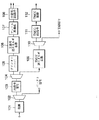
全体構成
図1に、BSデジタル放送の受信装置のブロック図を示し、このBSデジタル放送の受信装置について説明を行う。
【0052】
受信装置100は、復調部101と、第1のデマルチプレクサ102と、内符号復号部103と、第2のデマルチプレクサ104と、デインタリーバ105と、主信号逆エネルギー拡散部106と、フレーム再構成部107と、主信号RS復号部108と、TMCC逆エネルギー拡散部109と、第3のデマルチプレクサ110と、TMCCRS復号部111と、TMCC制御部112とを備えて構成される。
【0053】
復調部101には、例えばパラボラアンテナ等で受信して得られたRF信号が入力される。復調部101は、RF信号に搬送波信号を乗算して、直交変調信号であるI信号、Q信号を復調する。また、この復調部101は、周波数変換、搬送波同期、タイミング同期、フレーム同期処理も行う。また、この復調部101は、BPSK変調されているTAB信号(同期ワード)からスーパーフレーム及びフレームの開始位置を検出する。復調されたI信号データ、Q信号データは、第1のデマルチプレクサ102に送出される。
【0054】
第1のデマルチプレクサ102は、復調部101で検出されたフレーム開始位置からシンボルをカウントし、所定のシンボル位置にあるバースト信号を、主信号データ及びTMCCデータ(TAB信号も含む)から分離する。バースト信号は、そのまま読み捨てられる。主信号データ及びTMCCデータは、内符号復号部103に送出される。
【0055】
内符号復号部104は、各シンボルの変調方式及び内符号符号化率に従って、デパンクチャリング処理及びビタビ復号を行う。内符号復号されたデータは、第2のデマルチプレクサ104に送出される。
【0056】
第2のデマルチプレクサ104は、主信号データと、TMCCデータ(TAB信号も含む)とを分離する。分離された主信号データは、デインタリーバ105に送出される。分離されたTMCCデータ(TAB信号も含む)は、TMCC逆エネルギー拡散処理部106に送出される。
【0057】
デインタリーバ105は、送信側で行われたインターリーブ処理と逆の規則に従い、主信号データをデインタリーブする。デインタリーブされた主信号は、主信号逆エネルギー拡散部106に送出される。
【0058】
主信号逆エネルギー拡散部106は、15次系列の疑似ランダム系列(PRBS)を、主信号データに対して1ビットずつ加算して、送信側で行われたエネルギー拡散処理に対する逆処理を行う。なお、疑似ランダム符号系列(PRBS)はスーパーフレームの先頭で初期化される。また、各スロットの先頭の1バイト目に対してはエネルギー拡散処理はされないが、この間も、PRBSの発生は継続する。逆エネルギー拡散された主信号データは、フレーム再構成部107に送られる。
【0059】
フレーム再構成部107は、伝送時において削除されたトランスポートパケット(TSP)の同期ワード(0x47)を付加する処理等の送信側のデータフレームに対応したフレーム構造にデータ構造を再構成する。再構成された主信号データは、主信号リード・ソロモン復号部108に送出される。
【0060】
主信号リード・ソロモン復号部108は、204バイトからなる伝送パケット単位で、RS(204,188)のRS復号を行い、TSPを出力する。
【0061】
TMCC逆エネルギー拡散処理部109は、1スーパーフレーム分のTMCCデータ及びTAB信号をバッファに蓄積したのち、9次の疑似ランダム系列(PRBS)を、TMCCデータ及びTAB信号に対して1ビットずつ加算して、送信側で行われたエネルギー拡散処理に対する逆処理を行う。なお、この疑似ランダム符号系列(PRBS)はスーパーフレームの先頭で初期化される。また、TAB信号に対してはエネルギー拡散は行わないが、PRBSの発生は継続する。エネルギー拡散されたTMCCデータ及びTAB信号は、第3のデマルチプレクサ110に送出される。
【0062】
第3のデマルチプレクサ110は、TMCCデータとTAB信号とを分離する。分離されたTAB信号は、読み捨てられる。分離されたTMCCデータは、TMCCリード・ソロモン復号部111に送出される。
【0063】
TMCCリード・ソロモン復号部111は、64バイトからなるTMCCデータを、RS(64,48)のRS復号を行い、TMCC情報を出力する。RS復号されたTMCC情報は、TMCC制御部112に送出される。
【0064】
TMCC制御部112は、TMCC情報から伝送路復号に必要なTMCCデータを抽出し、各トランスポートストリーム(TS)に対応したTMCC情報を得るとともに、復号に必要な情報を各機能ブロックに配信する。
【0065】
受信装置100は、以上のような構成により、BSデジタル放送を受信して、MEPG−2システムに準拠したトランスポートストリームを復調する。
【0066】
復調部の構成
図2に、BSデジタル受信装置100の復調部101の構成を示し、この復調部101についてさらに説明する。
【0067】
復調部101は、第1の乗算器121と、第2の乗算器122と、局部発振器123と、90度移相器124と、第1のローパスフィルタ125と、第2のローパスフィルタ126と、第1のアナログ/デジタル(A/D)変換器127と、第2のアナログ/デジタル(A/D)変換器128と、搬送波補正部129と、第1の波形整形フィルタ130と、第2の波形整形フィルタ131と、タイミング同期部132と、フレーム同期部133と、搬送波同期部134と、第3の乗算器135と、第4の乗算器136と、パラレル/シリアル(P/S)変換器137と、スライサ138とを備えて構成される。
【0068】
例えば、パラボラアンテナ等により受信されたRF信号は、第1の乗算器121及び第2の乗算器122に入力される。
【0069】
局部発振器123は、周波数fc′、初期位相th′のcos波である搬送波を発生する。周波数fc′及び初期位相th′は、送信側の搬送波とは一致せず異なる周波数となる。発生された搬送波は、90度移相器124及び第1の乗算器121に供給される。
【0070】
90度移相器124は、cos波である搬送波を90度位相を進ませ、sin波を生成する。生成したsin波は、第2の乗算器122に供給される。
【0071】
第1の乗算器121は、受信信号とcos波とを乗算し、I信号を直交復調する。第2の乗算器122は、受信信号とsin波とを乗算し、Q信号を直交復調する。復調されたI信号は、第1のローパスフィルタ125により高域成分が除去されて第1のA/D変換器127に供給される。また、復調されたQ信号は、第2のローパスフィルタ126により高域成分が除去されて第2のA/D変換器128に供給される。
【0072】
第1のA/D変換器127は、I信号をデジタル化する。また、第2のA/D変換器128は、Q信号をデジタル化する。第1のA/D変換器127及び第2のA/D変換器128は、タイミング同期部132から出力されるサンプリングクロックCLKによってI信号及びQ信号をサンプリングする。このときサンプリング周波数は、送信側の伝送シンボルクロックと周波数及び位相が同期するように、タイミング同期部132により制御される。デジタル化されたI信号データ及びQ信号データは、それぞれ搬送波補正部129に供給される。
【0073】
搬送波補正部129は、搬送波同期部134から出力される回転位相補正信号(RI,RQ)を、第1及び第2のA/D変換器127,128から出力されたI信号データ及びQ信号データに、複素乗算する。I信号データ及びQ信号データは、この回転位相補正信号(RI,RQ)が複素乗算されることによって、受信側の局部発振器123により発生された搬送波の周波数fc′及び位相th′と送信側の搬送波の周波数fc及び位相thとの間で生じている周波数ずれ及び位相ずれが補正される。すなわち、搬送波周波数誤差及び位相誤差が補正される。補正されたI信号データは、第1の波形整形フィルタ130により波形整形がされた後、第3の乗算器135に供給される。位相補正がされたQ信号データは、第2の波形整形フィルタ131により波形整形がされた後、第4の乗算器136に供給される。
【0074】
タイミング同期部132は、A/D変換器127,128のサンプリングクロックを制御することによって、タイミング同期処理を行う回路である。タイミング同期部132は、波形整形フィルタ130,131により波形整形された受信データのクロック誤差を検出し、このクロック誤差が0となるようなサンプリングクロック、即ち、送信側の伝送シンボルのシンボルクロックに対して位相及び周波数が同期したサンプリングクロックを生成する。タイミング同期部132は、例えば、0交差法を用いてクロック誤差を検出する。生成されたクロックは、第1のA/D変換器127及び第2のA/D変換器128のサンプリングクロックとして用いられる。
【0075】
なお、タイミング同期部132は、波形整形フィルタ130,131から出力されるI,Q信号データに、搬送波周波数誤差および位相誤差が含まれていたとしても、受信C/N=0dBに対しても所定の特性が得られるだけのタイミング同期特性を有しているものとする。
【0076】
フレーム同期部133は、伝送データ内のTAB信号(同期ワード)を検出することによって、フレームの開始位置を検出するフレーム同期処理を行う回路である。
【0077】
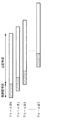
ここで、BSデジタル放送では、スーパーフレームと呼ばれるデータ構造が規定されている。スーパーフレームは、図3に示すように、8個のフレーム(フレーム#0〜フレーム#7)から構成されている。各フレームは、制御信号部(TMCC信号とTAB信号(同期ワード))と、主信号部(主信号とバースト信号)とから構成されている。
【0078】
主信号部は、図4に示すように、1フレームあたり48個のスロット(スロット#0〜スロット#47)により構成されている。主信号部は、203シンボルの主信号データと、BPSK変調(r=1/2)された4シンボルのバースト信号とが交互に配置されて構成されている。
【0079】
制御信号部は、1フレームあたり8バイトのTMCC(Transmission and Multiplexing Configuration Control)信号と、その前後に付加された2バイトずつのTAB信号(同期ワード)により構成される。TMCC信号とTAB信号は、それぞれBPSK変調(r=1/2)されており、伝送シンボル数でいうと、TMCCが128シンボル、TAB信号がそれぞれ32シンボルとなる。ここで、TMCCの前段に付けられているTAB信号は、その値がW1(0x1B95)とされている。また、TMCCの後段に付けられているTAB信号は、第1フレーム#0に対してはその値がW2(0xA340)とされており、第2〜8フレームに対してはその値がW3(0x5CBF)とされている。W2とW3とは、ビット反転した関係となっている。
【0080】
従って、このTAB信号(同期ワード)を検出することによって、フレームの同期をとることができ、また、W2とW3とを区別して検出することによって、スーパーフレームの同期をとることができる。なお、2バイトのTAB信号は、実際には畳み込み符号化され、32ビットの伝送シンボルとなる。そのうち、前半の12ビットは、前のフレームの最後の主信号データの影響を受けており値は不定であるが、後半の20ビットは前のフレームの影響が及ばない範囲であり、固定値となる。受信側では、この畳み込み符号化された固定値(W1に対してw1、W2/W3に対してw2/w3)を同期信号として検出することとなる。
【0081】
フレーム同期部133は、タイミング同期がとられているが、搬送波同期はとられていない状態で、このフレーム同期処理を行う。具体的には、タイミング同期がとられている伝送データに対して、シンボル間の差分演算を行う。そして、この差分演算されたビット列と、差分演算した同期ワードとの相関をとる。そして、その相関が最も高いシンボル位置(或いは、ある閾値より高い相関値のシンボル)を検出し、そのシンボル位置をフレームの同期位置とする。なお、TAB信号のW2とW3とは、ビット反転した関係にあるので、シンボル間の差分演算を行うと、値が同一になる。
【0082】
フレーム同期部133は、このようなTAB信号を検出して、フレーム開始位置を示すフレーム開始フラグ(FSTフラグ)、及び、スーパーフレームの開始位置を示すスーパーフレーム開始フラグ(SFSTフラグ)を生成する。また、フレーム同期部133は、FSTフラグ及びSFSTフラグだけではなく、SFSTフラグからシンボル数を計数することによって、TAB信号(同期ワード)のシンボル位置を示すTABフラグ、TMCCのシンボル位置を示すフラグであるTMCフラグ、主信号のシンボル位置を示すフラグであるDENフラグ、バースト信号のシンボル位置を示すフラグであるBRSTフラグも生成し出力してもよい。フレーム開始信号(FST)及びスーパフレーム開始フラグ(SFST)は、搬送波同期部134に供給される。
【0083】
また、フレーム同期部133は、180度位相反転信号も生成する。後述する搬送波同期部134は、180度の位相不確定性を許容する搬送波同期方式(搬送波同期を行ったときに位相が180度回転して同期がかかる可能性がある方式)をとっている。そのため、このフレーム同期部133は、同期ワード(TAB信号)のビット反転状態を検出して、180度の搬送波位相誤差を検出する。180度の搬送波位相誤差が検出された場合には、180度位相反転信号を−1として出力し、180度の搬送波位相誤差が検出されない場合には、180度位相反転信号を+1として出力する。この180度位相反転信号は、第3の乗算器135及び第4の乗算器136に供給される。
【0084】
なお、搬送波同期部134が180度の位相不確定性を残さずに搬送波同期を行える場合には、180度位相反転信号を常に+1としておくか、或いは、第3の乗算器135、第4の乗算器136及び180度位相反転信号を省略すればよい。また、フレーム同期部133は、タイミング同期部132によりタイミング同期がとられている状態で、フレーム同期動作を行う。そして、フレーム同期部133は、搬送波同期がとれていないという条件のもとで、受信C/N=0dBに対しても所定の特性が得られるだけのフレーム同期特性を有しているものとする。
【0085】
搬送波同期部134は、受信データの搬送波周波数誤差及び位相誤差に応じた回転位相補正信号(RI,RQ)を生成し、搬送波の同期処理を行う。受信データの搬送波周波数誤差及び位相誤差は、局部発振器123の搬送波の周波数ずれ及び位相ずれによって生じるものである。
【0086】
具体的には、搬送波同期部134は、直交座標系である受信データを角度データに変換し、その角度データが本来の受信点からどれだけ回転しているかを示す回転位相誤差を検出する。そして、その回転位相誤差をフィルタリングし、回転位相誤差の周波数成分及び位相成分を検出する。そして、この搬送波同期部134は、この検出した回転位相誤差の周波数成分及び位相成分を、キャンセルするような周波数及び位相の回転位相補正信号(RI,RQ)を、VCO等により生成する。搬送波補正部129は、この回転位相補正信号(RI,RQ)を、受信データに複素乗算して、搬送波周波数誤差及び位相誤差をキャンセルする。
【0087】
なお、搬送波同期部134は、タイミング同期部132によりタイミング同期がとられており、且つ、フレーム同期部133によりフレーム同期がとられているという状態で、搬送波同期動作を行う。そして、搬送波同期部134は、タイミング同期及びフレーム同期がとれているという条件のもとで、また、受信C/N=0dBに対しても所定の特性が得られるだけの搬送波同期特性を有しているものとする。
【0088】
第3の乗算器135は、第1の波形整形フィルタ130により波形整形されたI信号データと、フレーム同期部133から供給された180度位相反転信号とを乗算する。180度位相反転信号が+1であれば、I信号データはそのままで出力される。180度位相反転信号が−1であれば、I信号データの符号が反転して出力される。出力されたI信号データは、P/S変換部137に供給される。
【0089】
第4の乗算器136は、第2波形整形フィルタ131により波形整形されたQ信号データと、フレーム同期部133から供給された180度位相反転信号とを乗算する。180度位相反転信号が+1であれば、Q信号データはそのままで出力される。180度位相反転信号が−1であれば、Q信号データの符号が反転して出力される。出力されたQ信号データは、P/S変換部137に供給される。
【0090】
P/S変換器137は、I信号データ、Q信号データの順で受信データを選択して、シリアルデータに変換する。生成されたシリアルデータは、スライサ138に供給される。
【0091】
スライサ138は、入力データがある所定の値より大きい場合には0を出力し、入力データがある所定の値より小さい場合には1を出力する。
【0092】
そして、このスライサ138から復調データが出力され、内符号復号部103に供給される。
【0093】
復調部の同期動作フロー
図5に復調部の同期動作フローを示し、この復調部の同期動作について説明をする。
【0094】
まず、システムのリセット動作(ステップS1)がされると、タイミング同期の引き込み処理(ステップS)2に遷移する。
【0095】
タイミング同期の引き込み処理(ステップS2)では、タイミング同期部132が、波形整形フィルタ130,131の出力信号を検出し、A/D変換器127,128のサンプリングクロックの同期制御を行う。タイミング同期が確立すると、タイミング同期が完了した通知を発行し、次のフレーム同期の引き込み処理(ステップS3)に推移する。
【0096】
なお、タイミング同期の引き込み処理時(ステップS2)において、フレーム同期の引き込み処理及び搬送波同期の引き込み処理も並行して行ってる場合には、タイミング同期が完了した通知を特に発行しなくてもよい。もっとも、タイミング同期が確立しなければフレーム同期の引き込み処理及び搬送波同期の引き込み処理ができないので、これらの引き込み動作を停止しておいてもよい。このタイミング同期の引き込み処理時にフレーム同期の引き込み処理、搬送波同期の引き込み処理の動作を停止しておけば、消費電力の節約等ができる。このタイミング同期が確立した後は、以後、このタイミング同期が確立した状態が保護され続ける。
【0097】
続いて、フレーム同期の引き込み処理(ステップS3)では、フレーム同期部133が、波形整形フィルタ130,131の出力信号を検出し、その出力信号のシンボル間の差分データと同期ワードの差分データとの相関をとって、フレーム同期タイミングを検出する。フレーム同期タイミングが検出されると、フレーム同期が完了した通知を発行し、次の搬送波同期の引き込み処理(ステップS4)に推移する。
【0098】
なお、フレーム同期の引き込み処理(ステップS3)において、搬送波同期の引き込み処理を並行して行っている場合には、フレーム同期が完了した通知を発行しなくてもよい。もっとも、フレーム同期タイミングが検出されなければ搬送波同期の引き込み処理が困難なので、この搬送波同期の引き込み動作を停止しておいてもよい。このフレーム同期の引き込み処理時に、搬送波同期の引き込み処理の動作を停止しておけば、消費電力の節約等ができる。このフレーム同期が確立した後は、以後、このフレーム同期が確立した状態が保護され続ける。
【0099】
続いて、搬送波同期の引き込み処理(ステップS4)では、搬送波同期部134が、波形整形フィルタ130,131の出力信号から、フレーム同期部133から出力されたフレーム同期タイミングに基づき特定されるシンボルの位相回転誤差量を検出し、この位相回転誤差を補正する周波数及び位相の位相回転補正信号を生成する。この生成された位相回転補正信号は、搬送波補正部129に供給され、伝送データと複素乗算されることにより、搬送波誤差が補正される。
【0100】
そして、この搬送波誤差が補正され搬送波同期が確立すると、以後、タイミング同期の保護、フレーム同期の保護及び搬送波同期の保護がされた状態に推移する(ステップS5)。
【0101】
なお、以上の処理中に、タイミング同期が外れた場合には、タイミング同期の引き込み処理(ステップS2)に推移し、このステップ2から処理が続行される。また、フレーム同期が外れた場合には、フレーム同期の引き込み処理(ステップS3)に推移し、このステップS3から処理が続行される。また、搬送波同期が外れた場合には、搬送波同期の引き込み処理(ステップS4)に推移し、このステップS4から処理が続行される。
【0102】
このように、タイミング同期、フレーム同期、搬送波同期といった順序で、同期動作を行うことによって、復調部101では、複数の変調方式が採用され各変調方式が動的に変化するデジタル衛星放送の各種同期を簡易な構成で確実に検出することができる。また、劣悪な受信環境下においても小さな回路規模で確実に同期を検出することができる。
【0103】
フレーム同期部
つぎに、フレーム同期部133についてさらに詳細に説明を行う。
【0104】
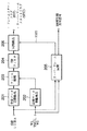
図6にフレーム同期部133のブロック構成図を示す。
【0105】
フレーム同期部133は、受信データ差動検出回路201と、同期ワード差動検出回路202と、フレーム相関回路203と、IIRフィルタ204と、スーパーフレーム同期回路205と、同期検出回路206とを備えて構成されている。
【0106】
受信データ差動検出回路201には、受信データが1シンボル毎入力される。
この受信データ差動検出回路201は、現在の時刻のシンボルと、1サイクル前のシンボルの複素共役とを複素乗算することによって、シンボル間の差動検出を行う。差動検出した結果得られる差動受信データは、フレーム相関回路203に供給される。
【0107】
同期ワード差動検出回路202は、フレームの先頭位置を示す同期ワードに対して、シンボル間の差動検出を行う。差動検出した結果得られる差動同期ワードデータは、フレーム相関回路203に供給される。
【0108】
フレーム相関回路203は、差動受信データが1シンボル毎に順次入力され、この差動受信データと差動同期ワードデータとの相関を算出する。フレーム相関回路203は、算出した相関値を1シンボル毎に出力していく。フレーム相関回路203から出力される相関値データは、IIRフィルタ204に供給される。
【0109】
IIRフィルタ204は、フレーム周期の遅延メモリを用いて、相関値データをIIRフィルタリングする。IIRフィルタリングされた相関値データは、同期検出回路206に供給される。
【0110】
スーパーフレーム同期回路205は、受信データが1シンボル毎に順次入力され、この受信データと同期ワードとの相関を算出する。ここで、スーパーフレーム同期回路205は、同期ワードw1と、同期ワードw2との相関をそれぞれ独立に算出し、搬送波同期が180度回転して同期がかかっているかどうかを検出する。また、このスーパーフレーム同期回路205は、同期ワードw1と、同期ワードw2との相関をそれぞれ独立に算出し、スーパーフレームの開始位置のフレームを検出する。なお、このスーパーフレーム同期回路205は、搬送波同期がかかった後に動作が可能となるものであればよい。
【0111】
同期検出回路206は、IIRフィルタ204から出力された相関値データに基づき、フレームの開始位置を検出し、フレームの開始位置を示すFSTフラグを出力する。また、同期検出回路206は、スーパーフレーム同期回路205から出力に基づき、スーパーフレームの開始位置を示すSFSTフラグを出力する。
【0112】
ここで、受信データと同期ワードとの相関を算出するにあたり、受信データを差動化する理由は、以下のとおりである。
【0113】
すなわち、受信データのシンボルに搬送波周波数誤差が含まれている場合、伝送路で雑音が付加されていなくとも、搬送波周波数誤差に対応する位相分1サンプル毎に進む。このような搬送波周波数誤差を含んだ入力シンボルを、サンプル毎に位相を検出して同期ワードと比較しても、正確に同期ワードのシンボル位置を検出することができない。それに対して、シンボル間で差動化することによって、各サンプルに含まれている搬送波周波数誤差が除去される。そのため、サンプル毎に一定の搬送波位相誤差成分のみが含まれている位相のシンボルとなるこのとき、差動化したシンボルと比較される同期ワードも同じく差動化しておけばよい。従って、受信データを差動化することによって、搬送波同期がとられておらず搬送波周波数誤差が含まれている受信データに対してフレーム同期をとることができる。なお、同期ワードのw2及びw3は、ビット反転の関係にあるため、差動をとれば、同一の値となる。
【0114】
また、受信データと同期ワードとの相関をとることによってフレームの同期を検出することができる理由及び相関値をフィルタリングする理由は、以下のとおりである。
【0115】
伝送されてくるシンボルに関して、同期ワード以外のシンボルはエネルギー拡散によって疑似的にランダム化されており、差動化した場合も同様にランダム化されていると考えられる。したがって、差動化した入力シンボルと差動化した同期ワードとの相関を計算することによって、同期ワードの挿入位置を検出することができる。すなわち、シンボル毎に相関を計算したとき、同期ワード位置では相関結果が最大値となり、同期ワードの位置以外では相関結果がほぼ0となるので、相関結果が最大値となる時刻が同期ワード位置であるといえる。
【0116】
もっとも、実際の運用では伝送路において雑音が付加され、相関結果にも影響を及ぼす。すなわち、同期ワードが挿入されている位置にもかかわらず相関結果が最大値より小さく出力されたり、同期ワード位置以外の位置でも相関結果がより大きく出力されたりする。したがって、このような雑音の影響を除去することが重要となる。そこで、同期ワードが周期的に伝送されることに着目する。上記のように相関結果が影響されるのは雑音の影響であると考えられるので、平均的には、同期ワードの挿入位置では相関結果が大きく出力され、同期ワード位置以外では相関結果がほぼ0となる。この性質を利用して、相関結果をフィルタリングすることによって雑音成分を低減し、同期ワード情報を強調することができる。すなわち、1フレーム内の先頭からpシンボル目の位置における相関値に対して、フレーム内のあるpシンボル目の位置における瞬時相関値を計算し、その結果を1フレーム前の先頭からpシンボル目の出力結果を用いてフィルタリングすることによって、フレーム内のそのpの位置における平均的な相関値を得ることができる。この処理を1フレーム内の全ての位置に対して行うことによって、各位置における平均的な相関値が得られる。
【0117】
フレームの同期検出方法、搬送波同期の180度の位相不確定性の除去方法及びスーパーフレームの同期検出方法は以下のとおりである。
【0118】
IIRフィルタリングされることにより、フレームの同期位置では相関値が大きく出力され、フレーム同期位置以外では相関値がほぼ0となるので、同期検出部206では、相関値の平均がもっとも大きくなる位置を同期位置として検出すればよい。また、フレーム同期位置以外では相関値がほぼ0となることから、相関値が所定の値よりも大きくなる位置を同期位置としてもよい。ここでは、装置の簡単化のため、相関値の値が所定の値よりも大きな位置を同期位置として検出するものとする。なお、このとき、同期位置検出結果の精度を高めるとともに、雑音による外乱を防ぐ目的でフレーム同期保護も行う。
【0119】
また、同期検出回路206は、搬送波同期が180度の位相不確定性を許容する場合、180度の位相不確定性の除去も行う。180度の位相不確定性は、搬送波同期がとられた後の受信シンボルから、同期ワードのw1のビットが正転か、反転かを検出することにより、判断している。
【0120】
また、同期検出回路206は、スーパーフレームの同期も検出している。スーパーフレームの同期は、搬送波同期がとられた後の受信シンボルから、同期ワードのw2が付加されているのか、同期ワードw3が付加されているのかを検出することにより、判断している。同期ワードw2が付加されているフレームがスーパーフレームの開始フレームとなる。
【0121】
各サブブロックの詳細な回路構成例
つぎに、フレーム同期回路133を構成する各サブブロックの回路構成例について説明をする。
【0122】
(差動検出回路)
図7に受信データ差動検出回路201の回路構成図を示す。
【0123】
受信データ差動検出回路201は、第1の遅延回路251と、第2の遅延回路252と、第1の乗算回路253と、第2の乗算回路254と、加算回路255と、第3の乗算回路256と、第4の乗算回路257と、減算回路258とを備えて構成される。
【0124】
第1の遅延回路251は、1シンボル分のI信号データを格納して、1サイクル分遅延させる。第2の遅延回路252は、1シンボル分のQ信号データを格納して、1サイクル分遅延させる。第1の乗算回路253は、現在の時刻のI信号データと、第1の遅延回路252に格納されている1サイクル前のI信号データとを乗算する。第2の乗算回路254は、現在の時刻のQ信号データと、第2の遅延回路253に格納されている1サイクル前のQ信号データとを乗算する。加算回路255は、第1の乗算回路253と第2の乗算回路254との出力を加算する。加算した出力が差動受信データのI信号成分(DI)となる。
【0125】
第3の乗算回路256は、現在の時刻のQ信号データと、第1の遅延回路251に格納されている1サイクル前のI信号データとを乗算する。第4の乗算回路257は、現在の時刻のI信号データと、第2の遅延回路252に格納されている1サイクル前のQ信号データとを乗算する。減算回路258は、第3の乗算回路256の出力から第4の乗算回路257の出力を減算する。減算した出力が差動受信データのQ信号成分(DQ)となる。
【0126】
すなわち、受信データ差動検出回路201は、
(DI,DQ)=(Ik,Qk)×(Ik-1,Qk-1)?
=(Ik×Ik-1+Qk×Qk-1 ,Qk×Ik-1−Ik×Qk-1)
といった演算を行う。なお、kはシンボル番号、(Ik-1,Qk-1)?は、(Ik-1,Qk-1)の共役複素数である。
【0127】
なお、同期ワードは、BPSK変調されているので、本来、差動結果のQ成分は常にゼロであり、後段の相関を求める際には使用されない。そのため、図中点線で囲んだ第3の乗算器256、第4の乗算器257及び減算回路258は、削除してもよい。
【0128】
また、同期ワード差動検出回路202は、この受信データ差動検出回路201と同一の回路構成となる。もっとも、TAB信号(同期ワード)は、既知の値であるので、予めTAB信号の差動演算結果をメモリに有しておけば、TAB用差動検出回路202は、特に設ける必要はない。
【0129】
(フレーム相関回路)
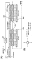
図8(A)にフレーム相関回路203の回路構成図を示す。
【0130】
フレーム相関回路203は、符号器301と、シフトレジスタ302と、第1のTABメモリ303と、第2のTABメモリ304と、相関演算器305とを備えて構成される。
【0131】
まず、受信データ用相関回路201には、差動化された受信データのI信号成分(DI)が、1シンボル毎に入力されてくる。
【0132】
符号器301は、差動受信データ(DI)が正数のとき0を出力し、負数のとき1を出力する。このよう符号化するのは、相関回路の回路規模削減のためである。このように符号化をすることによって、差動化された入力シンボルに対して硬判定を行い、その硬判定結果を用いて相関を計算していることに相当することとなる。符号器301の出力は、シフトレジスタ302に入力される。
【0133】
シフトレジスタ302は、1サイクル毎にに差動受信データのシフト動作を行う。格納するシンボル数は、192シンボル分である。
【0134】
第1のTABメモリ303は、19シンボル分の差動同期ワードw1を格納している。第2のTABメモリ304は、19シンボル分の差動同期ワードw2/w3を格納している。
【0135】
第1のTABメモリ303及び第2のTABメモリ304がそれぞれ19シンボル分のみのデータしか格納していないのは、以下のような理由によるものである。
【0136】
シンボル間で差動化していない状態の同期ワードw1、TMCC、同期ワードw2/w3は、図9(A)に示すように、それぞれ32シンボル、128シンボル、32シンボルで構成されている。ここで、同期ワードは、全て既知であり、その値は受信側で予めわかる。しかしながら、BSデジタル放送では、内符号の符号化方式として、拘束長7の畳み込み符号化又はトレリス符号化が行われている。そのため、同期ワードの前半12シンボル分は、その値が過去のデータに影響され、既知とならない。従って、同期ワードのうちで相関を求めることができるシンボルは、後半20シンボルに対してのみとなる。さらに、この相関回路では、受信データに対してシンボル間の差動化を行っている。従って、図9(B)に示すように、相関をとることが可能な既知のシンボル数が1シンボル分減少する。
【0137】
なお、同期ワードw1の20シンボル分のデータは、具体的には、以下のような値となる。
w1=1110_1100_1101_0010_1000
このw1の差動化をすると以下のような値となる。
w1(Diff)=001_1010_1011_1011_1100
同期ワードw2の20シンボル分データは、以下のような値となる。
w2=0000_1011_0110_0111_0111
同期ワードw3の20シンボル分データは、以下のような値となる。
w3=1111_0100_1001_1000_1000
この同期ワードw1、w2の差動化をすると以下のような値となる。
w2(Diff)=w3(Diff)=000_1110_1101_0100_1100
相関演算器305は、同期ワードw1の相関を演算する19個の演算器と、同期ワードw2/w3の相関を演算する19個の演算器から構成されている。同期ワードw1の相関を演算する19個の演算器は、シフトレジスタ302の第14シンボルから第33シンボルに格納されている値がi1として入力され、第1のTABメモリ303に格納されている値(即ち、同期ワードw1の差動シンボル)がi2として入力される。また、w2演算器は、シフトレジスタ302の第173シンボルから192シンボルに格納されている値がi1として入力され、第2のTABメモリ304に格納されている値(即ち、同期ワードw2/w3の差動シンボル)がi2として入力される。
【0138】
各演算器は、図8(B)に示すような演算を行う。
【0139】
すなわち、S0=f(i1,i2)+Si
f(i1,i2)は、i1=i2のときは1となり、i1≠i2のときは−1となる関数である。また、i1は、シフトレジスタ302に格納されている値で、i2は、TABメモリに格納されている値である。
【0140】
つまり、この相関演算器305は、以下のような差分受信データと差分同期ワードとの内積演算をしていることにほかならない。
diff(I,Q)・diff(TAB)
= diff(I,Q)[0] * diff(TAB)[0] + diff(I,Q)[1] * diff(TAB)[1] + ...
ここで、「・」は内積を示し、「*」はf(i1,i2)の演算を表している。
【0141】
そして、この38個の全演算器の演算結果が、1サイクル毎に全て累加算され、その1サイクル毎の累加算値が、相関値データとして出力される。
【0142】
従って、このような受信データ用相関回路201は、最も相関が高い場合には、相関値データとして、38という値を出力することとなる。
【0143】
なお、ここでは、相関値を1サイクル毎にシーケンシャルに求める回路を示したが、同時並行的、或いは、トーナメント型に演算を行ってもよいし、演算器を繰り返し使用して最終的な相関値を求めてもよい。
【0144】
(IIRフィルタ)
つぎに、IIRフィルタ204について説明をする。
【0145】
図10に、IIRフィルタ204の回路構成図を示す。
【0146】
IIRフィルタ204は、第1の増幅器351と、加算器352と、シフトレジスタ353と、第2の増幅器354とを備えている。
【0147】
第1の増幅器351は、フレーム相関回路205から出力された相関値データが入力される。第1の増幅器351は、相関値データに所定の利得Kを乗算する。利得Kが乗算された相関値データは、加算器352に供給される。
【0148】
加算器352は、第1の増幅器351からの出力と、第2の増幅器354からの出力を加算する。加算結果は、シフトレジスタ353に供給されるとともに、相関値データのフィルタリング結果として出力される。
【0149】
シフトレジスタ353は、1フレームに含まれるシンボル数分のワード数(39936ワード)のレジスタからなる。シフトレジスタ353は、入力されたデータ順に相関値データを格納し、1サイクル毎に格納している相関値データをシフトしていく。すなわち、シフトレジスタ353は、相関値データを1フレーム分遅延させる。最終段のレジスタに格納されている1フレーム分遅延した相関値データは、第2の増幅器354に供給される。
【0150】
第2の増幅器354は、シフトレジスタ353から出力された相関値データに、利得(1−K)を乗算する。乗算した結果は、加算器532に供給される。
【0151】
このようなIIRフィルタ204では、現在の時刻の相関値データと、1フレーム前に出力された相関値データとを適当な重み付けを行って加算している。すなわち、1フレーム間隔毎に取り出した相関値データに対して、それぞれ適当な重み付けをして、平均化している。また、重み付けを決定する利得Kは、雑音帯域を決める働きをもっている。
【0152】
(同期検出回路)
つぎに、同期検出回路について説明をする。
【0153】
図11に、同期検出回路206の回路構成図を示し、図12に、この同期検出回路206のフラグ制御を行うステートマシーンを示している。
【0154】
この同期検出回路206は、図11に示した論理回路と、図12に示したステートマシーン550により構成され、IIRフィルタ204によってフィルタリングされた相関値データからフレーム開始位置を検出するフレーム同期の引き込み動作(後方保護)を行うとともに、フレーム同期が確立したのちのフレーム同期の保護動作(前方保護)を行う回路である。
【0155】
論理回路では、IIRフィルタ204から出力された平均化された相関値と予め設定されている比較値とを比較する比較動作、現在のシンボル位置が確実にフレーム同期位置(同期ワードw1,w2/w3が発生する位置)であるかどうかを判定する同期位置判定動作、フレーム開始位置を示すフレームスタートフラグ(FSTフラグ)の発行動作、並びに、スーパーフレームの開始位置を示すスーパーフレームスタートフラグ(SFSTフラグ)の発行動作を行う。
【0156】
ステートマシーン550では、フレーム同期の引き込み中の状態(後方保護の状態)、フレーム同期の保持の状態(前方保護の状態)とで、その状態を分けて制御が行われる。ステートマシーン550は、フレーム同期の保持状態(前方保護の状態)であるかを示す同期確立フラグlockを発行して、論理回路に供給する。この同期確立フラグは、同期が確立しているときには有効(1)とされ、同期引き込み中のときには無効(0)とされる。また、ステートマシーン550は、論理回路に設けられるカウンタ及びレジスタの初期値をロードするロードフラグld4を発行する。このロードフラグld4は、初期値のロードタイミングに有効(1)とされ、それ以外のタイミングでは無効(0)とされる。
【0157】
まず、図11に示す論理回路の具体的な回路構成について説明をする。
【0158】
同期検出回路206は、第1の比較器501と、セレクタ502と、主同期判定回路503と、NAND回路504と、シンボルカウンタ505と、第2の比較回路506と、第3の比較器507と、レジスタ508と、第4の比較器509と、同期間隔判定回路510と、フレームカウンタ511と、第5の比較器512と、AND回路513とから構成されている。
【0159】
第1の比較器501には、IIRフィルタ204から出力された平均化された相関値Corrと、予め設定されている比較値Thとが入力される。第1の比較器501は、相関値Corrと比較値Thと比較して、Corr≧Thのときに有効(1)、Corr<Thのときに無効(0)という出力をする。
【0160】
比較値Thは、同期引き込み時(後方保護時)と、同期確立後の同期保持時(前方保護時)とで、その値がセレクタ502により切り換えられる。この切り替えは、ステートマシーン550から出力される同期確立フラグlockにより制御される。同期引き込み時に用いられる比較値Thは、同期保持時に用いられる比較値Thよりもより大きくしている。これは、同期引き込み時には、同期保持時よりも厳しい条件でフレーム開始位置が判断し、誤った位置で同期引き込みを行わないようにするためである。
【0161】
主同期判定回路503は、現在のシンボル位置がフレーム同期位置(同期ワードが発生される位置)であるかどうかを示す同期位置判定結果(ok,ng)を発生する回路である。この主同期判定回路503は、第1のAND回路531と、第2のAND回路532とから構成されている。第1のAND回路531は、第1の比較器501の比較結果と、判定動作有効フラグENとのAND論理演算をする。第1のAND回路531の演算結果は、okフラグとして出力される。第2のAND回路531は、第1の比較器501の比較結果の反転信号と、判定動作有効フラグENとのAND論理演算をする。第2のAND回路531の演算結果は、ngフラグとして出力される。
【0162】
ここで、判定動作有効フラグENは、NAND回路504から発行される。NAND回路504は、同期確立フラグlockと、同期確立時に同期ワードの発生予定位置を示すこととなる同期位置フラグTimingの反転信号とのNAND論理演算をして、判定動作有効フラグENを発行する。この判定動作有効フラグENは、同期引き込み時(後方保護時)には常に有効(1)とされる。また、この判定動作有効フラグは、同期保持時(前方保護時)には、同期ワードの発生予定位置でのみ有効(1)とされ、それ以外の時には無効(0)とされる。
【0163】
このような主同期判定回路503により発行される同期位置判定結果(ok,ng)は、以下のような意味となる。
(0,0):判定動作を行っていない(同期確立状態ではあるが、同期ワードの発生予定位置ではない)
(0,1):同期位置ではない
(1,0):同期位置である
(1,1):定義されていない。
【0164】
シンボルカウンタ505は、シンボル数をカウントするカウンタ回路である。シンボルカウンタ505は、1フレームのシンボル数(0〜39935)を周期的にカウントする。すなわち、シンボルカウンタ505は、シンボルクロックをインクリメントしていき、その値が39935となると、次にカウント値が0となるといったカウンタである。また、シンボルカウンタ505は、カウンタ値のロード機能を有している。このシンボルカウンタ505は、ステートマシーン550から与えられるロードフラグld4が有効(1)とされると、同期ワードの発生予定位置(TAB2の終了シンボル位置)を示す“191”の次の値である“192”が、カウンタ値としてロードする。ここで、シンボルカウンタ505にカウント値“192”がロードされるタイミングは、同期処理開始直後(リセット直後)の最初に同期位置が発見されたとき(すなわち、リセット後の最初に主同期判定回路503のokフラグが有効(1)となったとき)、及び、フレーム同期が確立するとき(一旦同期が外れて再び同期が確立するときも含む)である。また、シンボルカウンタ505は、カウンタ値が“39935”の最終値となったタイミングで、キャリーアウトフラグcoが有効(1)となる。
【0165】
第2の比較器506は、シンボルカウンタ505のカウント値が、フレーム同期検出シンボル位置(TAB2の終了シンボル位置)のシンボル番号である“191”となったときに、同期位置フラグTimingを有効(1)とする。この同期位置フラグTimingは、フレーム同期が確立している状態のときに、同期ワードの発生予定位置(TAB2の終了シンボル位置)のタイミングを示すこととなる。 この同期位置フラグTimingは、同期確立フラグlockが有効(1)となっているときにのみ判定動作有効フラグENに反映される。
【0166】
第3の比較器507は、シンボルカウンタ505のカウント値が、フレームの開始位置のシンボル番号である“0”となったときに、フレームの開始位置を示すFSTフラグを有効(1)とし、それ以外のシンボルタイミングではFSTフラグを無効(0)とする。
【0167】
レジスタ508は、主同期判定回路503のokフラグが有効(1)となったときに、シンボルカウンタ505のカウント値を取り込んで、その値を保持する回路である。すなわち、レジスタ508は、主同期判定回路503により同期位置であると判定されたときにシンボルカウンタ505により発生されたカウント値を保持する。また、レジスタ508は、レジスタ値のロード機能を有しており、ステートマシーン550からのロードフラグld4が有効(1)とされると、フレーム同期位置(TAB2の終了位置のシンボル番号)を示す“191”がレジスタ値としてロードされる。
【0168】
第4の比較器509は、シンボルカウンタ505のカウント値と、レジスタ508のカウント値とを比較する。比較した結果、値が一致すれば有効(1)、値が一致しなければ無効(0)という出力をする。
【0169】
同期間隔判定回路510は、okフラグが、フレーム間隔(39936シンボル)毎に発行されているかどうかを判定する回路である。同期間隔判定回路510は、okフラグの発生間隔が1フレーム期間となっているかどうかを示す同期間隔判定結果(ok2,ng2)を発行する。具体的には、同期間隔判定回路510は、第3のAND回路533と、第4のAND回路534とから構成されている。第3のAND回路533は、第4の比較器509の比較結果と、okフラグとのAND論理演算をする。第3のAND回路533の演算結果は、ok2フラグとして出力される。第4のAND回路534は、第4の比較器509の比較結果の反転信号と、okフラグとのAND論理演算をする。第4のAND回路534の演算結果は、ng2フラグとして出力される。
【0170】
この同期間隔判定回路510により出力される同期間隔判定結果(ok2,ng2)は、前回okフラグが有効(1)となったときのシンボルカウンタ505のカウント値と、現在のシンボルカウンタ505のカウント値とを比較した結果である。つまり、同期間隔判定回路510は、前回の同期位置と判別されたカウンタ値と、今回同期位置と判別されたカウンタ値とが一致しているかどうかを判別している。すなわち、同期間隔判定回路510は、シンボルカウンタ505が1フレーム周期でカウント値を発生することから、1フレーム周期で同期位置が発生されているかどうかを判断していることとなる。ここで、同期位置が1フレーム周期で発生され続ければ、その同期位置はフレームの同期位置として確からしいものと考えらる。従って、ok2フラグが連続して発生されれば、同期引き込み状態から同期確立状態に遷移させてもよいと判断できる。なお、後述するステートマシーン550では、ok2フラグが連続して3回発行されると、同期を確立させた前方保護状態に遷移させている。
【0171】
また、一方、同期引き込み時におけるカウント値及びレジスタ値は、特に受信データのシンボル番号と同期がとられていなくても、フレーム同期の引き込みを行うことができ、同期確立の直前にカウント値及びレジスタ値を正確な値にロードする回路構成となっている。そのため、もし同期状態から同期がはずれたとしても、シンボルカウンタ505は、カウント値を初期化や停止をせずに、同期保持状態から連続してカウントを継続して、同期引き込み状態に遷移させることができる。従って、なんらかのノイズによってフレーム同期位置で相関値が低くなってしまい、フレーム同期が外れたとしても、カウンタ値は保持されたままととなり、或いは、再引き込み時に偶然同期位置以外で判定結果がokとなってしまったとしても、FSTフラグは正確に発行され続けることとなる。
【0172】
このような同期間隔判定回路510により発行される同期間隔判定結果(ok2,ng2)は、以下のような意味となる。
(0,0):判定動作を行っていない(okフラグが有効(1)となっておらず、同期位置ではない)
(0,1):前回のokフラグからの間隔が1フレーム周期となっていない
(1,0):前回のokフラグからの間隔が1フレーム周期となっている
(1,1):定義されていない。
【0173】
フレームカウンタ511は、シンボルカウンタ505のキャリアウトのタイミングを、8カウント周期でカウントするカウンタである。フレームカウンタ511は、カウンタ値のリセット機能を有しており、詳細を後述するスーパーフレーム同期回路205からのFST0フラグ(フレーム番号0を示すフラグ)によってカウンタ値が0にリセットされる。スーパーフレームの同期が確立された後は、このフレームカウンタ511のカウント値が、フレーム番号を示すこととなる。
【0174】
第5の比較器512は、フレームカウンタ511のカウント値が0となっているときに有効(1)となる。
【0175】
AND回路513は、第3の比較器507から出力されるFSTフラグと、第5の比較器512からの比較結果とのAND論理演算を行うことによって、スーパーフレームの開始位置を示すSFSTフラグを発行する。すなわち、フレーム番号が0のフレームの開始位置をスーパーフレームの開始位置として出力する。
【0176】
以上のように同期検出回路206では、フレームの同期位置を示すフレームスタートフラグ(FSTフラグ)及びスーパーフレームの同期位置を示すスーパーフレームフラグ(SFSTフラグ)を発行することができる。
【0177】
つぎに、図12に示すステートマシーンを説明しながら、同期検出回路206の動作について説明を行う。
【0178】
ステートマシーン550には、okフラグ、ngフラグ、ok2フラグ、ng2フラグ、リセットフラグが入力される。
【0179】
また、ステートマシーン550からは、同期確立フラグlock、及び、カウンタ値及びレジスタ値のロードフラグld4が出力される。
【0180】
また、ステートマシーン550には、内部状態として、以下の状態M、状態0〜7がある。
状態M:リセット直後の状態
状態0:同期ワードの位置探索状態にある非同期状態(後方保護)
状態1:同期ワードの位置確認状態にある非同期状態(後方保護)
状態2:同期ワードの位置確認状態にある非同期状態(後方保護)
状態3:同期ワードの位置確認状態にある非同期状態(後方保護)
状態4:同期ワードの位置確認状態にある同期状態(前方保護)
状態5:同期ワードの位置確認状態にある同期状態(前方保護)
状態6:同期ワードの位置確認状態にある同期状態(前方保護)
状態7:同期ワードの位置確認状態にある同期状態(前方保護)。
【0181】
以下各状態について説明をしていく。
【0182】
---状態M---
まず、ステートマシーン550は、リセットフラグが入力されると状態Mに遷移する。このとき、シンボルカウンタ505のカウンタ値及びレジスタ508のレジスタ値は、不定の状態である。 okフラグが有効(1)となったタイミングで、ロードフラグld4を有効(1)とし、シンボルカウンタ505のカウンタ値に“192”をロードし、レジスタ508のレジスタ値に“191”をロードする。そして、状態1に遷移する。
【0183】
なお、この状態Mでは、同期確立フラグlockが無効(0)とされていて、同期引き込み用の比較値Thが第1の比較器501に入力される。また、同期位置判別回路503に入力される判定動作有効フラグENも常に有効(1)となっており、相関値Corr≧比較値Thであれば、常にokフラグが発行される状態である。
【0184】
---状態1---
状態1は、フレーム同期引き込みの後方保護状態であり、同期間隔判定結果(ok2,ng2)により状態が次に遷移する。ok2フラグが有効(1)となれば、次の状態2に遷移し、ng2フラグが有効(1)となれば、状態0に遷移する。ここで、この状態1では、シンボルカウンタ505のカウンタ値が、伝送されているデータのシンボル位置を正確に示しているとは限らないが、okフラグが有効(1)となったときのカウンタ値が、前回のカウンタ値と一致すれば、次の状態に遷移することとなる。すなわち、okフラグの発行周期が1フレームとなっていればが同期間隔判定結果ok2フラグが発行されるので次の状態2に遷移し、okフラグの発行周期が1フレームとなっていなければ、ng2フラグが発行されるので状態0に戻る。なお、この状態1では、ロードフラグld4は無効(0)とされ、同期確立フラグも無効(0)とされている。
【0185】
---状態2---
状態2も、状態1と同様に、フレーム同期引き込みの後方保護状態であり、同期間隔判定結果(ok2,ng2)により状態が次に遷移する。ok2フラグが有効(1)となれば、次の状態3に遷移し、ng2フラグが有効(1)となれば、状態0に遷移する。また、この状態1でも、ロードフラグld4は無効(0)とされ、同期確立フラグも無効(0)とされている。
【0186】
---状態3---
状態3は、フレーム同期引き込みの後方保護状態であり、同期間隔判定結果(ok2,ng2)により状態が次に遷移する。ok2フラグが有効(1)となれば、次の状態4に遷移し、ng2フラグが有効(1)となれば、状態0に遷移する。
【0187】
ここで、この状態3では、okフラグが有効(1)となったタイミングで、ロードフラグld4を有効(1)として、シンボルカウンタ505のカウンタ値に“192”をロードし、レジスタ508のレジスタ値に“191”をロードする。また、次の状態4に遷移するときに、同期確立フラグlockを有効(1)とし、以後、論理回路500を同期確立状態で動作させる。すなわち、このステートマシーン550では、3回連続して、okフラグの発行位置が同一のカウント値であった場合には、フレーム同期が確立したものと判断し、以後、フレーム同期を保持する前方向保護状態に遷移する。そして以後、同期確立状態(状態4,状態5,状態6,状態7)では、シンボルカウンタ505のカウンタ値が、伝送されているデータのシンボル位置を正確に示している判断し、以後の処理が行われる。
【0188】
---状態4---
状態4は、フレーム同期確立時の前方向保護状態であり、同期位置判定結果(ok,ng)により状態が次に遷移する。okフラグが有効(1)となれば、この状態4を繰り返し、ngフラグが有効(1)となれば、状態5に遷移する。なお、この状態4では、同期確立フラグlockが有効(1)とされ、同期保持用の比較値Thが第1の比較器501に入力される。また、同期位置判別回路503に入力される判定動作有効フラグENは、シンボルカウンタ505のカウンタ値が191となったときにのみ、有効(1)となり、このタイミングでのみ、相関値Corrと比較値Thとの比較が行われる。
【0189】
---状態5---
状態5は、フレーム同期確立時の前方向保護状態であり、同期位置判定結果(ok,ng)により状態が次に遷移する。okフラグが有効(1)となれば、状態4に遷移し、ngフラグが有効(1)となれば、状態6に遷移する。なお、この状態5でも、状態4と同様に、同期確立フラグlockが有効(1)されている。
【0190】
---状態6---
状態6は、フレーム同期確立時の前方向保護状態であり、同期位置判定結果(ok,ng)により状態が次に遷移する。okフラグが有効(1)となれば、状態4に遷移し、ngフラグが有効(1)となれば、状態7に遷移する。なお、この状態6でも、状態4と同様に、同期確立フラグlockが有効(1)されている。
【0191】
---状態7---
状態7は、フレーム同期確立時の前方向保護状態であり、同期位置判定結果(ok,ng)により状態が次に遷移する。okフラグが有効(1)となれば、状態4に遷移し、ngフラグが有効(1)となれば、状態0に遷移する。なお、この状態7でも、状態4と同様に、同期確立フラグlockが有効(1)されている。
【0192】
ここで、この状態7で、ngフラグが有効(1)となると、同期保持状態(前方保護状態)から同期がはずれたことを示し、以後、状態0からの引き込み状態に移る。このようにこのステートマシーン550では、4回連続して同期が外れた場合に、再度引き込み状態に移るようにしており、例えば、ノイズ等により偶発的に同期がはずれた場合であっても、すぐに引き込み動作を行わないようにしている。
【0193】
---状態0---
状態0は、フレーム同期引き込みの後方保護状態であり、同期間隔判定結果(ok,ng)により状態が次に遷移する。okフラグが有効(1)となれば、次の状態1に遷移し、ngフラグが有効(1)となれば、この状態0を繰り返す。ここで、この状態0では、シンボルカウンタ505のカウンタ値を、新たに更新していない。そのため、例えば、偶発的に同期が外れ、同期引き込み状態となっても、シンボルカウンタ505のカウント値はリセットされず、そのままカウントが続行されることとなる。もっとも、シンボルカウンタ505のカウント値が、伝送されているデータのシンボル位置を正確に示しているとは限らないが、okフラグが有効(1)となったときのカウンタ値が、前回のカウンタ値と一致しているかどうかを判断しているので、okフラグの発行周期が1フレームとなっているかどうかは、確実に判断することができる。
【0194】
(スーパーフレーム同期回路)
つぎに、スーパーフレーム同期回路について説明をする。
【0195】
スーパーフレーム同期回路205は、受信データと同期ワードとの相関を算出し、後段の同期ワードがw2であるかw3であるかを検出して、スーパーフレーム開始位置を検出する。これとともに、スーパーフレーム同期回路205は、受信データと同期ワード(w1)との相関を算出し、この同期ワードw1が反転しているかどうかを検出して、搬送波同期が180度回転して同期がかかっているかどうかを検出する。なお、スーパーフレーム同期回路205は、搬送波同期が確立した後に動作をすればよい。そのため、搬送波誤差を除去するために、シンボル間で差動演算することなく、相関を検出をすることができる。
【0196】
このスーパーフレーム同期回路205の構成図を図13に示す。スーパーフレーム同期回路205は、この図13に示すように、相関回路561と、同期検出回路562とから構成される。
【0197】
相関回路561は、受信データのI信号成分が1シンボル毎に順次入力され、この受信データと、同期ワードw1,w2との相関を算出する。相関回路561は、算出した相関値を1シンボル毎に出力していく。相関回路561から出力される相関値データは、同期検出回路562に供給される。
【0198】
同期検出回路562は、相関回路561から出力された相関値データに基づき、フレーム番号0の開始位置(すなわち、スーパーフレームの開始位置)を検出し、FST0フラグを出力する。また、同期検出回路562は、相関回路561から出力された相関値データに基づき、搬送波同期が180度位相回転してかかっているかどうかを検出し、タイミング信号に同期させて、180度位相反転信号を出力する。
【0199】
図14(A)に、相関回路561の回路構成図を示す。
【0200】
相関回路561は、符号器571と、シフトレジスタ572と、第1のTABメモリ573と、第2のTABメモリ574と、w1相関演算器575と、w2相関演算器576とを備えて構成される。
【0201】
まず、相関回路561には、受信データのI信号成分(I)が、1シンボル毎に入力されてくる。
【0202】
符号器571は、受信データ(I)が正数のとき0を出力し、負数のとき1を出力する。このよう符号化するのは、相関回路の回路規模削減のためである。このように符号化をすることによって、入力シンボルに対して硬判定を行い、その硬判定結果を用いて相関を計算していることに相当することとなる。符号器571の出力は、シフトレジスタ572に入力される。
【0203】
シフトレジスタ572は、1サイクル毎にに受信データのシフト動作を行う。
格納するシンボル数は、例えば192シンボル分である。
【0204】
第1のTABメモリ573は、20シンボル分の同期ワードw1を格納している。第2のTABメモリ574は、20シンボル分の同期ワードw2を格納している。
【0205】
なお、同期ワードw1の20シンボル分のデータは、具体的には、以下のような値となる。
w1=1110_1100_1101_0010_1000
同期ワードw2の20シンボル分データは、以下のような値となる。
w2=0000_1011_0110_0111_0111
w1相関演算器575は、同期ワードw1の相関を演算する20個の演算器とから構成されている。w1相関演算器575は、シフトレジスタ572の第13シンボルから第33シンボルに格納されている値がi1として入力され、第1のTABメモリ573に格納されている値(即ち、同期ワードw1)がi2として入力される。また、w2相関演算器576は、シフトレジスタ572の第172シンボルから192シンボルに格納されている値がi1として入力され、第2のTABメモリ574に格納されている値(即ち、同期ワードw2)がi2として入力される。
【0206】
各演算器は、図14(B)に示すような演算を行う。
【0207】
すなわち、S0=f(i1,i2)+Si
f(i1,i2)は、i1=i2のときは1となり、i1≠i2のときは−1となる関数である。また、i1は、シフトレジスタ575に格納されている値で、iは、TABメモリに格納されている値である。
【0208】
そして、w1相関演算器575の20個の全演算器の演算結果が1サイクル毎に全て累加算され、その1サイクル毎の累加算値が、w1相関値データとして出力される。また、w2相関演算器576の20個の全演算器の演算結果が1サイクル毎に累加算され、その1サイクル毎の累加算値が、w2相関値データとして出力される。
【0209】
なお、シフトレジスタ572は、192個の一連のシフトレジスタとしているが、w1相関値データとw2相関値データとは、同時刻に出力される必要はないので、20個のシフトレジスタとしてもよい。この場合、TAB1が全て入力されたタイミングでw1との相関結果を演算し、その相関結果を保持しておき、また、TAB2が全て入力されたタイミングでw2との相関結果を演算し、その相関結果を保持しておき、同期検出回路562に供給してもよい。
【0210】
続いて、同期検出回路について説明をする。
【0211】
フレーム番号0の同期ワードは、w1とw2との組み合わせとなっている。一方、フレーム番号0以外のフレームの同期ワードは、w1とw3との組み合わせになっている。また、搬送波同期が180度位相回転している場合には、伝送データが全てビット反転する。そのため、スーパーフレームの先頭のフレーム(フレーム番号0)の検出及び搬送波同期の位相反転状態の検出は、
・フレーム同期タイミングにおけるTAB1の受信シンボルが正転しているか、反転しているかを判断する。
・TAB2の受信シンボルがw2であるかw3であるかを判断する。
ことにより行うことができる。
【0212】
ここで、受信データの正/反転を評価するためには、同期ワードの発生タイミングで得られるw1相関値データが整数であるか負数であるかを評価すればよい。w1相関値データが正数であれば、受信データは正転となる。また、w1相関値データが負数であればば、受信データは反転となる。すなわち、搬送波同期が180度回転している場合には、伝送データは、全てビット反転してしまうため、w1相関値データは、最も相関が低い値(具体的に先に示した図14の回路であれば−20という値となる。)となる。
【0213】
TAB2の受信シンボルがw2であるかw3であるかを判断するには、まず、フレーム同期タイミングにおけるw2相関値データが整数であるか負数であるかを評価する。そして、TAB1が正転であり、且つ、TAB2が正転であれば、TAB2に記述されている同期ワードはw2である。TAB1が正転であり、且つ、TAB2が反転であれば、TAB2に記述されている同期ワードはw3である。また、TAB1が反転であり、且つ、TAB2が正転であれば、TAB2に記述されている同期ワードはw3である。TAB1が反転であり、且つ、TAB2が反転であれば、TAB2に記述されている同期ワードはw2である。
【0214】
そして、TAB2がw2であれば、スーパーフレームの先頭フレーム(フレーム番号0)であるので、FST0フラグを有効(1)とし、TAB2がw3であれば、スーパーフレームの先頭フレームではない(フレーム番号1〜7)であるので、FST0フラグを無効(0)とする。
【0215】
具体的に、同期検出回路562の回路構成例としては、図15に示すように、第1の比較回路581と、第2の比較回路582と、EXOR回路583と、反転回路584と、第1のAND回路585と、第2のAND回路586と、ラッチ回路587とから構成されている。
【0216】
第1の比較回路581は、w1相関値データが正数であるか負数であるかを比較する。第1の比較回路581は、w1相関値データが、0以上であれば出力を有効(1)とし、w1相関値データが0未満であれば出力を無効(0)とする。
【0217】
第2の比較回路582は、w2相関値データが正数であるか負数であるかを比較する。第2の比較回路582は、w2相関値データが 0以上であれば出力を有効(1)とし、w2相関値データが0未満であれば出力を無効(0)とする。
【0218】
EXOR回路583は、第1の比較回路581と第2の比較回路582との出力が一致していれば、出力を有効(1)とし、不一致であれば無効(0)とする。
【0219】
反転回路584は、第1の比較回路581の出力を反転する。
【0220】
第1のAND回路585は、同期ワード発生タイミングtimingと、EXOR回路583の出力とのAND論理演算を行い、同期ワード発生タイミングtiming以外での検出出力をマスクする。
【0221】
第2のAND回路586は、同期ワード発生タイミングtimingと、反転回路585の出力とのAND論理演算を行い、同期ワード発生タイミングtiming以外での検出出力をマスクする。
【0222】
レジスタ回路587は、同期ワード発生タイミングtimingで、書き込み許可が当たられるレジスタであり、第2のAND回路586の出力値が書き込まれる。
【0223】
以上のような回路構成の同期検出回路562では、第1のAND回路585の出力が、FST0フラグとして出力され、レジスタ回路587の出力が180度位相反転信号として出力される。
【0224】
搬送波同期部
つぎに、搬送波同期部134についてさらに詳細に説明を行う。
【0225】
図16に搬送波同期部134のブロック構成図を示す。
【0226】
搬送波同期部134は、タイミング制御回路601と、誤差量検出回路602と、ループフィルタ604と、VCO(Voltage Controlled Oscillator)604とから構成される。
【0227】
タイミング制御回路601には、図2に示したフレーム同期回路133からフレームスタートフラグ(FSTフラグ)が入力される。タイミング制御回路601は、このFSTフラグから、シンボル数をカウントすることによって、TMCCデータ、TAB信号(同期ワード)、バースト信号等のBSデジタル放送で必ずBPSK変調されることが規定されているシンボルタイミングを特定する。タイミング制御回路601は、そのシンボルがTMCCデータ、TAB信号、バースト信号である場合に有効(1)となるBPSKフラグを生成し、ループフィルタ602に供給する。
【0228】
誤差量検出回路602には、図2に示した波形整形フィルタ130,131から出力されたI信号データ及びQ信号データが入力される。誤差量検出回路602は、入力されたシンボルに対する、BPSKの本来信号点からの位相誤差量又は周波数誤差量Δθを算出する。検出された誤差量Δθは、ループフィルタ603に供給される。
【0229】
ループフィルタ603は、例えば1次以上の遅れ要素を有し、入力された誤差量Δθを所定量の重み付けを行ってループフィルタリングを行う。ループフィルタ603は、フィルタリングした誤差量ΔθをVCO604に供給する。ここで、このループフィルタ603は、BPSKフラグに応じて、TMCC,TAB,バースト位置でのみ遅れ要素が更新される。そのため、VCO604に対する発振周波数の更新がTAB,TMCC,バースト位置でのみ行われ、それ以外の位置では、最後の制御値が保持される。すなわち、BPSKで変調されているシンボルの誤差量Δθのみを用いて、間欠的に搬送波同期の動作を行うことになる。
【0230】
例えば、ループフィルタ603は、誤差量Δθに定数Kを乗算する第1の乗算器611と、フィルタ出力に定数(1−K)を乗算する第2の乗算器612と、第1の乗算器611の出力と第2の乗算器612の出力とを加算する加算器613と、加算器613の出力を遅延させるレジスタ614とから構成される。この場合、レジスタ614と乗算器611及び加算器613でが遅れ要素を構成することになる。このレジスタ614は、BPSKフラグがイネーブル信号として入力され、BPSKフラグが有効(1)とされているときにのみ、内部データを更新する。
【0231】
VCO604は、例えばアキュミレータと(cosθ,sin-1θ)* 回路等により構成され、ループフィルタ603から出力をMod360°で累加算し、その加算結果を直交信号に変換して、搬送波誤差に応じた周波数の位相回転補正信号(RI,RQ)を出力する。なお、* は複素共役を示す。
【0232】
このように生成された位相回転補正信号は、図2に示す搬送波補正回路129に供給される。搬送波補正回路129では、この位相回転補正信号を受信信号に複素乗算することにより、受信信号に含まれている搬送波誤差成分を除去している。
【0233】
以上のように搬送波同期部134では、フレーム同期部133により求められたフレームスタートフラグ(FST)に基づきTAB、TMCC、バースト信号のシンボル位置を特定し、これらのシンボルに含まれている位相及び周波数誤差量に応じて搬送波誤差の補正をしている。
【0234】
ところで、この搬送波同期部134により搬送波の同期がとられた後は、スーパーフレームの同期がとられTMCC情報が復号される。そのため、一旦搬送波の同期がとられれば、TMCC情報を参照することによって、TAB,TMCC,バースト位置のみならず全シンボルの変調方式を特定することができる。
【0235】
そのため、搬送波同期が確立した後は、TAB,TMCC,バースト位置のみ用いて間欠的に搬送波同期処理を行わず、全シンボルの位相誤差量を検出して搬送波同期処理を行ってもよい。
【0236】
図17に全シンボルの位相誤差量を検出して搬送波同期処理を行う搬送波同期部650の回路構成図を示す。
【0237】
タイミング制御回路651は、フレームスタートフラグ(FSTフラグ)、スーパーフレームスタートフラグ(SFST)及びTMCC情報が入力される。タイミング制御回路651は、TMCC情報を解析するとともに、FSTフラグ及びSFSTフラグからシンボル数をカウントして、各シンボルの変調方式を特定する変調方式指定信号TMを生成する。変調方式指定信号TMは、誤差量検出回路652及びループフィルタ653に供給される。
【0238】
誤差量検出回路652には、図2に示した波形整形フィルタ130,131から出力されたI信号データ及びQ信号データが入力される。誤差量検出回路652は、入力されたシンボルに対する位相誤差量又は周波数誤差量Δθを算出する。ここで、誤差量検出回路652は、供給された変調方式指定信号に応じた信号点からの位相誤差量Δθを算出する。例えば、BPSK変調されたシンボルであれば、0及びπの信号点からの位相誤差を算出する。また、QPSK変調されたシンボルであれば、π/4、3π/4、5π/4及び7π/4の信号点からの位相誤差量を算出する。また、8PSK変調されたシンボルであれば、0,π/4,π/2,3π/4,π,5π/4,3π/2及び7π/4の信号点からの位相誤差量を算出する。検出した誤差量Δθは、ループフィルタ653に供給される。
【0239】
ループフィルタ653は、誤差量Δθに対する重み付けを可変して、フィルタリングを行う。このときの重み付けは、例えば、TAB,TMCC,バースト位置と主信号位置とで重み付けを変えたり、また、変調方式に応じて重み付けを変える。例えば、TAB,TMCC,バースト位置では大きい重み付けを行い、主信号位置では小さい重み付けを行う。また、BPSKには、最も大きい重み付けを行い、8PSKには最も小さい重み付けを行い、QPSKには中間の重み付けを行うようにする。
【0240】
このようなループフィルタ653は、例えば、誤差量Δθに定数Kを乗算する第1の乗算器661と、フィルタ出力に定数(1−K)を乗算する第2の乗算器662と、第1の乗算器661の出力と第2の乗算器662の出力とを加算する加算器663と、加算器663の出力を遅延させるレジスタ664とにより構成できる。ここで、第1の乗算器661及び第2の乗算器662の乗数Kを、変調方式情報TMに応じて変えることによって、ループ帯域を変更し、また、Gを変えることによってループ利得を変換し。重み付けを変えることが可能となる。
【0241】
なお、VCO654の機能は、VCO604と同一である。
【0242】
IIRフィルタの変形例
つぎに、フレーム同期部133に用いられているIIRフィルタの変形例について説明をする。
【0243】
図10に示したIIRフィルタは、1フレーム間隔毎に取り出した相関値データ毎に平均化を行うために、1フレーム分のワード数(39936ワード)のデータが格納可能なシフトレジスタを用いている。
【0244】
フレーム同期処理を行う場合、その引き込み時にはフレーム開始位置が確立されていないため、このように1フレーム分(39936ワード)のメモリ容量は必ず必要となる。しかしながら、フレーム同期が確立した後は、後段の同期検出回路206では、同期ワードの発生タイミングのシンボルのみデータしか必要とされていない。すなわち、フレーム同期が確立した後は、同期ワード発生位置での相関値データに対してのみフィルタリングを行っている。
【0245】
また、BSデジタル放送の受信装置では、例えば、RSデコーダ、デインタリーバ等の復号回路において、大量のメモリが使用される。しかしながら、これらの復号回路は、復調部においてタイミング同期、フレーム同期、搬送波同期が確立した後でなければ動作の必要がない。
【0246】
ここでは、フレーム同期の引き込み時には、エラー訂正回路やデインタリーバ等の後段の復号回路に用いられるメモリを用い、フレーム同期の確立後には、1ワード分の遅延メモリを用いるようにして、フレーム同期の引き込み時と確立後とでフィルタリングに使用する遅延メモリを切り換えるIIRフィルタについて説明をする。
【0247】
図18に、このIIRフィルタの回路構成図を示す。ここでは、RS復号部108に用いられるメモリを用いた例について説明をする。
【0248】
IIRフィルタ700は、第1の増幅器701と、加算器702と、入力セレクタ703と、エラー訂正用メモリ704と、遅延レジスタ705と、セレクタ706と、第2の増幅器707とを備えている。
【0249】
第1の増幅器701は、フレーム相関回路205から出力された相関値データが入力される。第1の増幅器701は、相関値データに所定の利得Kを乗算する。利得Kが乗算された相関値データは、加算器702に供給される。
【0250】
加算器702は、第1の増幅器701からの出力と、第2の増幅器707からの出力を加算する。加算結果は、入力セレクタ703及び遅延レジスタ705に供給される。
【0251】
入力セレクタ703は、RS復号部108からの出力データと、加算器702からの出力データとが入力される。入力セレクタ703は、図12(b)に示したステートマシーン550から出力される同期確立フラグlockにより、切り換えられる。この同期確立フラグlockは、フレーム同期が確立時には有効(1)とされ、フレーム同期の引き込み時には無効(0)とされるフラグである。入力セレクタ703は、同期確立フラグlockが有効(1)のときにはRS復号部108からのデータをエラー訂正用メモリ704に入力し、同期確立フラグlockが無効(0)のときには加算器702からのデータをエラー訂正用メモリ704に入力する。
【0252】
エラー訂正用メモリ704は、同期確立フラグlockが有効(1)の場合には、1フレーム分のデータ(39936ワード)のFIFOと同様に機能するように内部アドレスレジスタがデータの書き込み/読み出しを行う。また、同期確立フラグlockが無効(0)の場合には、RS復号部108からの制御に従いデータの書き込み/読み出しを行う。
【0253】
遅延レジスタ705は、1ワード分のデータを格納するレジスタである。遅延レジスタ705は、同期ワードの発生予定位置を示す同期位置フラグTimingが、イネーブル信号として入力される。この同期位置フラグTimingは、同期検出回路206から入力される。遅延レジスタ705は、この同期位置フラグTimingが有効(1)とされているときにのみ、データの更新を行う。
【0254】
出力セレクタ706は、エラー訂正用メモリ704からの出力データと、遅延レジスタ705からの出力データとが入力される。入力セレクタ703は、同期確立フラグlockにより切り換えられる。出力セレクタ706は、同期確立フラグlockが有効(1)のときには遅延レジスタ705からのデータを第2の増幅器707に供給し、同期確立フラグlockが無効(0)のときにはエラー訂正用メモリ704からのデータを第2の増幅器707に供給する。
【0255】
第2の増幅器707は、出力セレクタ706からの出力データに。利得(1−K)を乗算する。乗算した結果は、加算器702に供給される。
【0256】
このようなIIRフィルタ700では、フレーム同期の引き込み時には、エラー訂正用メモリ704を用いて、1フレーム間隔毎に取り出した相関値データに対して、適当な重み付けをして平均化している。そして、フレーム同期の確立後には、エラー訂正用メモリ704を解放する。そして、1ワード分のデータを格納する遅延レジスタ705を用いて、同期ワード(TAB信号)の発生タイミングで得られる相関値データを適当な重み付けをして平均化している。
【0257】
効果
以上のように本発明の実施の形態のBSデジタル放送の受信装置では、デジタル衛星放送の伝送データのシンボルタイミングの同期処理を行い、続いて、デジタル衛星放送の伝送データに含まれている同期ワードを検出することによってフレームタイミングの同期処理を行い、続いて、このフレーム同期タイミングに基づき少なくとも同期ワードの受信位相を検出して搬送波同期処理を行う。
【0258】
すなわち、このBSデジタル放送の受信装置では、フレーム同期処理を行った後に搬送波同期処理を行うようにしている。従って、非常に簡易な構成で搬送波同期処理を行うことができ、それとともに、変調方式が動的に変化するデジタル衛星放送の場合であっても、QPSKや8PSKといった信号点間の位相が狭いシンボルを用いずに、信号点間の位相が広いBPSK変調されたシンボルを検出して搬送波同期処理を行うので、高精度に搬送波同期処理を行うことができる。
【0259】
また、このBSデジタル放送の受信装置では、フレーム同期タイミングをとる際に、伝送データのシンボル間の差分データを検出し、この伝送データの差分データと同期ワードの差分データとの相関をとっている。そのため、搬送波誤差を除去した状態で同期ワード位置を特定することができ、非常に高精度にフレームの同期処理及び搬送波同期処理を行うことができる。
【0260】
また、このBSデジタル放送の受信装置では、フレーム同期タイミングをとる際に、伝送データの差分データと同期ワードの差分データとの相関値を、フレーム周期でフィルタリングを行っている。そのフィルタリングは、例えば、IIR(Infinite Impulse Response)フィルタを用いてフィルタリングを行っている。そのため、偶発的に生じるノイズ等の影響を除去することができ、より正確にフレーム同期処理及び搬送波同期処理を行うことができる。
【0261】
また、このBSデジタル放送の受信装置では、フレーム同期確立後には、同期ワードの発生位置のシンボルに対してのみフィルタリングを行うようにする。そして、フレーム同期の引き込み時には、フレーム同期が確立する前には使用されないエラー訂正用のメモリやデインタリーバ等のメモリ等の復号用メモリを用いてフィルタリングを行い、フレーム同期確立後には、1シンボル分のデータ容量の遅延メモリを用いてフィルタリングを行うようにしている。そのため、フィルタリングに必要となるメモリ容量を非常に少なくすることができる。
【0262】
また、このBSデジタル放送の受信装置では、上記相関値データと所定の値とを比較して同期位置を検出し、さらに、この同期位置の間隔と上記同期位置の間隔とを比較して同期間隔を検出する。そして、伝送データのシンボル数を1フレーム周期でカウントするシンボルカウンタを用い、上記同期間隔が所定回連続して1フレーム間隔となった後に、そのカウント値が初期値とされ、以後、このカウント値が所定の値となったときにフレーム開始信号を発行するようにしている。そのため、簡易な構成で確実にフレーム同期位置を検出し、さらに、フレーム同期が確立した後にも確実にフレーム同期を保持することができる。
【0263】
また、このBSデジタル放送の受信装置では、同期位置検出部により検出された上記同期位置及び上記同期間隔検出部により得られた上記同期間隔に基づき、シンボルカウンタのカウント値を伝送データに同期させるための同期引き込み状態と、シンボルカウンタのカウント値が伝送データに同期している状態を保持するための同期保持状態とを遷移するステートマシーンをを用いて、フレーム同期処理を制御している。そのため、フレーム同期の引き込み状態と、フレーム同期の保護状態とで、簡易にフレームの同期処理方式を切り換えることができる。
【0264】
【発明の効果】
本発明にかかるデジタル衛星放送復調装置及び方法では、デジタル衛星放送の伝送データのシンボルタイミングの同期処理を行い、続いて、デジタル衛星放送の伝送データに含まれている同期ワードを検出することによってフレームタイミングの同期処理を行い、続いて、このフレーム同期タイミングに基づき少なくとも同期ワードの受信位相を検出して搬送波同期処理を行う。
【0265】
すなわち、本発明によれば、フレーム同期処理を行った後に搬送波同期処理を行うようにしている。従って、非常に簡易な構成で搬送波同期処理を行うことができ、それとともに、変調方式が動的に変化するデジタル衛星放送の場合であっても、QPSKや8PSKといった信号点間の位相が狭いシンボルを用いずに、信号点間の位相が広いBPSK変調されたシンボルを検出して搬送波同期処理を行うので、高精度に搬送波同期処理を行うことができる。
【0266】
また、本発明では、フレーム同期タイミングをとる際に、伝送データのシンボル間の差分データを検出し、この伝送データの差分データと同期ワードの差分データとの相関をとっている。そのため、搬送波誤差を除去した状態で同期ワード位置を特定することができ、非常に高精度にフレームの同期処理及び搬送波同期処理を行うことができる。
【0267】
また、本発明では、フレーム同期タイミングをとる際に、伝送データの差分データと同期ワードの差分データとの相関値を、フレーム周期でフィルタリングを行っている。そのフィルタリングは、例えば、IIR(Infinite Impulse Response)フィルタを用いてフィルタリングを行っている。そのため、偶発的に生じるノイズ等の影響を除去することができ、より正確にフレーム同期処理及び搬送波同期処理を行うことができる。
【0268】
また、本発明では、フレーム同期確立後には、同期ワードの発生位置のシンボルに対してのみフィルタリングを行うようにする。そして、フレーム同期の引き込み時には、フレーム同期が確立する前には使用されないエラー訂正用のメモリやデインタリーバ等のメモリ等の復号用メモリを用いてフィルタリングを行い、フレーム同期確立後には、1シンボル分のデータ容量の遅延メモリを用いてフィルタリングを行うようにしている。そのため、フィルタリングに必要となるメモリ容量を非常に少なくすることができる。
【0269】
また、本発明では、上記相関値データと所定の値とを比較して同期位置を検出し、さらに、この同期位置の間隔と上記同期位置の間隔とを比較して同期間隔を検出する。そして、伝送データのシンボル数を1フレーム周期でカウントするシンボルカウンタを用い、上記同期間隔が所定回連続して1フレーム間隔となった後に、そのカウント値が初期値とされ、以後、このカウント値が所定の値となったときにフレーム開始信号を発行するようにしている。そのため、簡易な構成で確実にフレーム同期位置を検出し、さらに、フレーム同期が確立した後にも確実にフレーム同期を保持することができる。
【0270】
また、本発明では、同期位置検出部により検出された上記同期位置及び上記同期間隔検出部により得られた上記同期間隔に基づき、シンボルカウンタのカウント値を伝送データに同期させるための同期引き込み状態と、シンボルカウンタのカウント値が伝送データに同期している状態を保持するための同期保持状態とを遷移するステートマシーンをを用いて、フレーム同期処理を制御している。そのため、フレーム同期の引き込み状態と、フレーム同期の保護状態とで、簡易にフレームの同期処理方式を切り換えることができる。
【0271】
また、本発明では、直交座標信号からなる伝送データに対して、回転補正信号を複素乗算することによって搬送波誤差を補正し、搬送波誤差が補正された伝送データから位相回転誤差量を検出し、この位相回転誤差量に応じた回転補正信号を生成し、搬送波誤差が補正された伝送データの位相回転誤差量を同期ワードの変調方式に基づき算出し、フレーム同期タイミングからシンボル数をカウントして少なくとも同期ワードのシンボル位置を特定して、特定したシンボルの位相回転誤差量に対してフィルタリングを行い、フィルタリングされた位相回転誤差量に応じて周波数及び位相が制御された回転補正信号を生成することによって、搬送波同期処理を行う。
【0272】
このため、非常に簡易な構成で搬送波同期処理を行うことができ、それとともに、変調方式が動的に変化するデジタル衛星放送の場合であっても、QPSKや8PSKといった信号点間の位相が狭いシンボルを用いずに、信号点間の位相が広いBPSK変調されたシンボルを検出して搬送波同期処理を行うので、高精度に搬送波同期処理を行うことができる。
【0273】
また、本発明では、搬送波同期の確立後には、スーパーフレームスタート開始位置とTMCC情報とに基づき主信号の変調方式を特定することによって、同期ワード、バースト信号及び/又はTMCC信号のみならず、主信号の誤差量も検出して、搬送波同期を行う。そのため、より確実に搬送波同期を行うことができる。
【図面の簡単な説明】
【図1】本発明を適用したBSデジタル放送の受信装置のブロック構成図である。
【図2】上記BSデジタル放送の受信装置の復調部のブロック構成図である。
【図3】BSデジタル放送信号のスーパーフレーム構造を説明するための図である。
【図4】BSデジタル放送信号のフレーム構造を説明するための図である。
【図5】上記復調部の同期処理手順を示すフローチャートである。
【図6】上記復調部のフレーム同期部のブロック構成図である。
【図7】上記フレーム同期部の差動検出回路の回路図である。
【図8】上記フレーム同期部の相関回路の構成図である。
【図9】同期ワードのデータ構成を説明するための図である。
【図10】上記フレーム同期部のIIRフィルタの構成図である。
【図11】上記フレーム同期部の同期検出部の回路図である。
【図12】上記同期検出部のステートマシーンを示す図である。
【図13】上記同期検出部のスーパーフレーム同期回路のブロック構成図である。
【図14】上記スーパーフレーム同期回路の相関回路の構成図である。
【図15】上記スーパーフレーム同期回路の同期回路の回路図である。
【図16】上記復調部の搬送波同期部のブロック構成図である。
【図17】搬送波同期部の他の構成例を示すブロック構成図である。
【図18】上記IIRフィルタの他の構成例を示す構成図である。
【図19】デジタル直交変調を行ってデジタルデータの伝送をする場合の一般的な伝送モデルを示すブロック構成図である。
【図20】QPSKの信号点配置とそのアイパターンを示す図である。
【図21】8PSKの信号点配置とそのアイパターンを示す図である。
【符号の説明】
101 復調部、121 第1の乗算器、122 第2の乗算器、123 局部発振器、124 90度移相器、125 第1のローパスフィルタ、126 第2のローパスフィルタ、127 第1のアナログ/デジタル変換器、128 第2のアナログ/デジタル変換器、129 搬送波補正部、130 第1の波形整形フィルタ、131 第2の波形整形フィルタ、132 タイミング同期部、133 フレーム同期部、134 搬送波同期部[0001]
BACKGROUND OF THE INVENTION
The present invention relates to a digital satellite broadcast demodulating device and a digital satellite broadcast demodulating method for demodulating digital satellite broadcast.
[0002]
[Prior art]
FIG. 19 is a block diagram showing a general transmission model when digital quadrature modulation is performed to transmit digital data.
[0003]
The transmission system Tx includes a data generator 11, a serial / parallel (S / P)
[0004]
The data generator 11 of the transmission system Tx generates digital data obtained by serializing I signal data and Q signal data. The generated digital data is supplied to a serial / parallel (S / P)
[0005]
The S /
[0006]
The
[0007]
The −90 degree phase shifter 14 delays the phase of the carrier wave, which is a cosine wave, by 90 degrees, and generates a −sin wave. The generated -sin wave is supplied to the
[0008]
The
[0009]
The quadrature modulation signal is subjected to waveform shaping and amplification by the
[0010]
The transmission line (Channel) includes an
[0011]
The reception system Rx includes a
[0012]
The received signal is input to the
[0013]
The
[0014]
The 90-degree phase shifter 24 advances the phase of the carrier wave, which is a cos wave, by 90 degrees to generate a sin wave. The generated sin wave is supplied to the
[0015]
The
[0016]
The first A /
[0017]
The carrier
[0018]
The
[0019]
The
[0020]
The P /
[0021]
The
[0022]
Then, transmission data is reproduced from the
[0023]
In such digital data transmission, the reception side reproduces the transmission symbol clock generated on the transmission side and performs demodulation processing. This reproduction of the transmission symbol clock is called timing reproduction. On the receiving side, it is also possible to obtain a correct demodulation result by correcting the symbol clock of the received signal by some means instead of regenerating the transmission symbol clock. The process of obtaining the correct demodulation result by correcting the transmission symbol, including the timing reproduction and the demodulation process, is called timing synchronization.
[0024]
On the receiving side, demodulation processing is performed by reproducing the coordinate system defining the transmission symbol space generated on the transmitting side. This reproduction of the coordinate system of the transmission symbol space is called carrier wave reproduction. On the receiving side, a correct demodulation result can be obtained by correcting the coordinate system defining the symbol space of the received signal by some means, instead of reproducing the coordinate system defining the transmission symbol space. . Obtaining a correct demodulation result by correcting the coordinate system defining the transmission symbol space, including reproducing the coordinate system defining the transmission symbol space and performing demodulation processing, is called carrier wave synchronization.
[0025]
[Problems to be solved by the invention]
By the way, in CS digital broadcasting whose service has already been started in Japan, all transmission signals are QPSK modulated. The signal point arrangement of QPSK is defined on, for example, the symbol space shown in FIG. 20A, and the eye pattern of the received signal after passing through the waveform shaping filter is shown in FIG. 20B for both the I and Q axes. become that way. That is, in the QPSK modulation method, 1-bit information is assigned to each of the I signal and the Q signal, and data for modulating the I signal and the Q signal can be defined independently of each other.
[0026]
On the other hand, in the BS digital broadcasting system in Japan, three types of modulation systems of BPSK, QPSK, and 8PSK are adopted, and each modulation system changes dynamically.
[0027]
The signal point arrangement of 8PSK is defined on, for example, the symbol space shown in FIG. 21A, and the eye pattern of the received signal after passing through the waveform shaping filter is shown in FIG. become that way. Therefore, in the case of 8PSK, when the zero crossing method is applied to perform timing synchronization, the detection level is lowered as compared with the QPSK signal, and the noise component of the detection result is increased.
[0028]
Here, when there is a phase error in the carrier wave generated from the local oscillator between the transmitting side and the receiving side, the received signal is received by being rotated by an angle corresponding to the error phase with respect to the transmitted signal. The Rukoto. When a frequency error exists in the carrier wave, the received signal is received by being rotated at an angular velocity corresponding to the error frequency with respect to the transmission signal.
[0029]
Therefore, on the receiving side, when carrier wave synchronization is performed, the phase error amount is usually detected from the reception signal point, and the phase error and the frequency error are corrected by feeding back the correction amount corresponding to the error phase component and the frequency error component. I am doing so.
[0030]
However, in the QPSK modulation system, the phase error detection range is 45 degrees, whereas in the 8PSK modulation system used in the BS digital broadcasting system, the phase error detection range is halved to 22.5 degrees, and phase detection is performed. Accuracy will deteriorate.
[0031]
Furthermore, in the case of BS digital broadcasting, in terms of the transmission environment, standardization has been formulated for TMCC data transmitted by the BPSK modulation method so as to ensure reliability at C / N = 0 dB. It is necessary to take measures against a very poor reception environment.
[0032]
The present invention provides a digital satellite broadcast receiving apparatus and reception method that reliably detect carrier synchronization of a digital satellite broadcast signal in which each modulation method dynamically changes, and also reliably detect synchronization even in a poor reception environment. The purpose is to provide.
[0033]
[Means for Solving the Problems]
In the digital satellite broadcast demodulator according to the present invention, the timing synchronization means for synchronizing the transmission data symbol timing, and the synchronization word is detected from the transmission data in which the timing is synchronized, and the frame synchronization timing of the transmission data is detected. And a carrier synchronization means for identifying a symbol position of at least the synchronization word based on the frame timing, detecting a reception phase of each symbol of the synchronization word, and performing carrier synchronization processing.
[0034]
This digital satellite broadcast demodulator performs symbol timing synchronization processing of digital satellite broadcast transmission data, and then performs frame timing synchronization processing by detecting a synchronization word included in the digital satellite broadcast transmission data. Subsequently, at least the reception phase of the synchronization word is detected based on the frame synchronization timing, and the carrier synchronization processing is performed.
[0035]
That is, in this digital satellite broadcast demodulator, the carrier wave synchronization process is performed after the frame synchronization process.
[0036]
The digital satellite broadcast demodulator according to the present invention detects difference data between symbols of transmission data when obtaining frame synchronization timing, and correlates the difference data of the transmission data with the difference data of the synchronization word. ing.
[0037]
The digital satellite broadcast demodulator according to the present invention filters the correlation value between the transmission data difference data and the synchronization word difference data according to the frame period when obtaining the frame synchronization timing. The filtering is performed using, for example, an IIR (Infinite Impulse Response) filter.
[0038]
In the digital satellite broadcast demodulating device according to the present invention, after the frame synchronization is established, filtering is performed only on the symbol at the position where the synchronization word is generated. Then, when pulling in the frame synchronization, filtering is performed using a decoding memory such as an error correction memory or a memory such as a deinterleaver that is not used before the frame synchronization is established. Filtering is performed using a delay memory having a data capacity of.
[0039]
In the digital satellite broadcast demodulating device according to the present invention, the correlation value data is compared with a predetermined value to detect a synchronization position, and the synchronization position interval is compared with the synchronization position interval. Detect synchronization interval. Then, using a symbol counter that counts the number of symbols of transmission data at a period of one frame, the count value is set as an initial value after the synchronization interval reaches a frame interval continuously for a predetermined number of times. A frame start signal is issued when becomes a predetermined value.
[0040]
In the digital satellite broadcast demodulator according to the present invention, the count value of the symbol counter is synchronized with the transmission data based on the synchronization position detected by the synchronization position detection unit and the synchronization interval obtained by the synchronization interval detection unit. A state machine that transitions between a synchronization pull-in state for maintaining the state of the symbol counter and a state in which the count value of the symbol counter is synchronized with the transmission dataTheIt is used to control the frame synchronization process.
[0041]
The digital satellite broadcast demodulator according to the present invention corrects a carrier wave error by performing complex multiplication of a rotation correction signal on transmission data composed of orthogonal coordinate signals, and performs phase rotation from the transmission data on which the carrier wave error is corrected. Detects the error amount, generates a rotation correction signal corresponding to the phase rotation error amount, calculates the phase rotation error amount of the transmission data with the carrier wave error corrected based on the synchronization word modulation method, and calculates the symbol from the frame synchronization timing. Count the number to identify at least the symbol position of the synchronization word, filter the phase rotation error amount of the specified symbol, and rotate correction with frequency and phase controlled according to the filtered phase rotation error amount Carrier wave synchronization processing is performed by generating a signal.
[0042]
According to the digital satellite broadcast demodulation method for demodulating a digital satellite broadcast signal according to the present invention, the synchronization timing of the transmission data symbol timing is detected, the synchronization word is detected from the transmission data synchronized in timing, and the transmission data Frame synchronization timing is detected, at least the symbol position of the synchronization word is specified based on the frame timing, and the reception phase of each symbol of the synchronization word is detected to perform carrier wave synchronization processing.
[0043]
That is, in this digital satellite broadcast demodulation method, the carrier wave synchronization process is performed after the frame synchronization process.
[0050]
DETAILED DESCRIPTION OF THE INVENTION
Hereinafter, a BS digital broadcast receiving apparatus according to an embodiment of the present invention will be described.
[0051]
overall structure
FIG. 1 is a block diagram of a BS digital broadcast receiver, and the BS digital broadcast receiver will be described.
[0052]
The receiving
[0053]
For example, an RF signal obtained by receiving with a parabolic antenna or the like is input to the
[0054]
The
[0055]
The inner
[0056]
The
[0057]
The
[0058]
The main signal inverse
[0059]
The
[0060]
The main signal Reed-
[0061]
The TMCC inverse energy
[0062]
The
[0063]
The TMCC Reed-
[0064]
The
[0065]
The receiving
[0066]
Demodulator configuration
FIG. 2 shows the configuration of the
[0067]
The
[0068]
For example, an RF signal received by a parabolic antenna or the like is input to the
[0069]
The
[0070]
The 90-
[0071]
The
[0072]
The first A /
[0073]
The carrier
[0074]
The
[0075]
Note that the
[0076]
The
[0077]
Here, in BS digital broadcasting, a data structure called a super frame is defined. As shown in FIG. 3, the super frame is composed of eight frames (
[0078]
As shown in FIG. 4, the main signal unit is composed of 48 slots (
[0079]
The control signal unit is composed of a TMCC (Transmission and Multiplexing Configuration Control) signal of 8 bytes per frame and a 2-byte TAB signal (synchronization word) added before and after that. The TMCC signal and the TAB signal are each BPSK modulated (r = 1/2), and in terms of the number of transmission symbols, the TMCC signal is 128 symbols and the TAB signal is 32 symbols. Here, the value of the TAB signal attached to the preceding stage of TMCC is W1 (0x1B95). The TAB signal attached to the subsequent stage of the TMCC has a value of W2 (0xA340) for the
[0080]
Accordingly, the frame can be synchronized by detecting this TAB signal (synchronization word), and the superframe can be synchronized by detecting W2 and W3 separately. Note that the 2-byte TAB signal is actually convolutionally encoded into a 32-bit transmission symbol. Among them, the first 12 bits are affected by the last main signal data of the previous frame and the value is indefinite, but the latter 20 bits are in a range not affected by the previous frame. Become. On the receiving side, this convolutionally encoded fixed value (w1 for W1 and w2 / w3 for W2 / W3) is detected as a synchronization signal.
[0081]
The
[0082]
The
[0083]
The
[0084]
If the
[0085]
The
[0086]
Specifically, the carrier
[0087]
The
[0088]
The
[0089]
The
[0090]
The P /
[0091]
The
[0092]
The demodulated data is output from the
[0093]
Demodulator synchronization operation flow
FIG. 5 shows a synchronization operation flow of the demodulation unit, and the synchronization operation of the demodulation unit will be described.
[0094]
First, when a system reset operation (step S1) is performed, the process proceeds to a timing synchronization pull-in process (step S) 2.
[0095]
In the timing synchronization pull-in process (step S2), the
[0096]
Note that when the timing synchronization pull-in process (step S2) is performed in parallel with the frame sync pull-in process and the carrier wave sync pull-in process, it is not particularly necessary to issue a notification that the timing synchronization has been completed. However, since the frame synchronization pull-in process and the carrier wave sync pull-in process cannot be performed unless the timing synchronization is established, these pull-in operations may be stopped. If the operation of the frame synchronization pull-in process and the carrier wave sync pull-in process is stopped during the timing synchronization pull-in process, power consumption can be saved. After this timing synchronization is established, the state in which this timing synchronization has been established continues to be protected.
[0097]
Subsequently, in the frame synchronization pull-in process (step S3), the
[0098]
In the frame synchronization pull-in process (step S3), when the carrier wave sync pull-in process is performed in parallel, it is not necessary to issue a notification that the frame synchronization has been completed. Of course, the carrier synchronization pull-in process is difficult if the frame synchronization timing is not detected, so the carrier synchronization pull-in operation may be stopped. If the operation of the carrier synchronization pull-in process is stopped during the frame synchronization pull-in process, power consumption can be saved. After this frame synchronization is established, the state in which this frame synchronization is established continues to be protected.
[0099]
Subsequently, in the carrier synchronization pull-in process (step S4), the
[0100]
When this carrier wave error is corrected and carrier wave synchronization is established, the timing synchronization protection, frame synchronization protection and carrier wave synchronization protection are followed (step S5).
[0101]
If the timing synchronization is lost during the above processing, the process proceeds to the timing synchronization pull-in processing (step S2), and the processing is continued from
[0102]
As described above, by performing the synchronization operation in the order of timing synchronization, frame synchronization, and carrier wave synchronization, the
[0103]
Frame synchronization unit
Next, the
[0104]
FIG. 6 shows a block configuration diagram of the
[0105]
The
[0106]
The reception data
The reception data
[0107]
The synchronization word
[0108]
The
[0109]
The
[0110]
The super
[0111]
The
[0112]
Here, the reason why the received data is differentiated in calculating the correlation between the received data and the synchronization word is as follows.
[0113]
That is, when a carrier frequency error is included in the symbol of the received data, even if no noise is added on the transmission path, the process proceeds by one sample for the phase corresponding to the carrier frequency error. Even if the phase of an input symbol including such a carrier frequency error is detected for each sample and compared with the synchronization word, the symbol position of the synchronization word cannot be accurately detected. On the other hand, the carrier frequency error included in each sample is removed by differentiating between symbols. For this reason, each sample has a phase symbol containing only a constant carrier wave phase error component, and at this time, the sync word to be compared with the differentiated symbol may also be differentiated. Therefore, by differentiating the received data, it is possible to achieve frame synchronization with respect to the received data that does not have carrier synchronization and includes a carrier frequency error. Since the synchronization words w2 and w3 are in a bit-inversion relationship, they have the same value if they are differentially taken.
[0114]
The reason why frame synchronization can be detected by correlating the received data with the synchronization word and the reason for filtering the correlation value are as follows.
[0115]
Regarding the transmitted symbols, symbols other than the synchronization word are pseudo-randomized by energy diffusion, and it is considered that the symbols are also randomized when they are differentiated. Therefore, the insertion position of the synchronization word can be detected by calculating the correlation between the differentiated input symbol and the differentiated synchronization word. That is, when the correlation is calculated for each symbol, the correlation result is the maximum value at the synchronization word position, and the correlation result is almost 0 at the position other than the synchronization word position. Therefore, the time when the correlation result is the maximum value is the synchronization word position. It can be said that there is.
[0116]
However, in actual operation, noise is added in the transmission path, which also affects the correlation result. That is, the correlation result is output smaller than the maximum value regardless of the position where the synchronization word is inserted, or the correlation result is output larger at positions other than the synchronization word position. Therefore, it is important to remove the influence of such noise. Therefore, attention is paid to the fact that the synchronization word is transmitted periodically. Since it is considered that the correlation result is influenced by noise as described above, on average, the correlation result is greatly output at the insertion position of the synchronization word, and the correlation result is almost 0 at other positions than the synchronization word position. It becomes. By utilizing this property, it is possible to reduce the noise component and enhance the synchronization word information by filtering the correlation result. That is, the instantaneous correlation value at the position of the p-th symbol in the frame is calculated with respect to the correlation value at the position of the p-th symbol from the head in one frame, and the result is calculated as the p-th symbol from the head in the previous frame. By filtering using the output result, an average correlation value at the p position in the frame can be obtained. By performing this process for all positions in one frame, an average correlation value at each position can be obtained.
[0117]
A frame synchronization detection method, a carrier synchronization 180-degree phase uncertainty removal method, and a superframe synchronization detection method are as follows.
[0118]
As a result of IIR filtering, the correlation value is output to a large value at the frame synchronization position, and the correlation value is almost zero at other than the frame synchronization position. Therefore, the
[0119]
The
[0120]
The
[0121]
Detailed circuit configuration example of each sub-block
Next, an example of the circuit configuration of each sub-block constituting the
[0122]
(Differential detection circuit)
FIG. 7 shows a circuit configuration diagram of the reception data
[0123]
The reception data
[0124]
The
[0125]
The
[0126]
That is, the received data
(DI, DQ) = (Ik, Qk) × (Ik-1, Qk-1)?
= (Ik× Ik-1+ Qk× Qk-1 , Qk× Ik-1-Ik× Qk-1)
The operation is performed. K is a symbol number and (Ik-1, Qk-1)?(Ik-1, Qk-1) Is a conjugate complex number.
[0127]
Since the synchronization word is BPSK-modulated, the Q component of the differential result is always always zero and is not used when obtaining the correlation at the subsequent stage. Therefore, the
[0128]
The synchronous word
[0129]
(Frame correlation circuit)
FIG. 8A shows a circuit configuration diagram of the
[0130]
The
[0131]
First, the received
[0132]
The
[0133]
The
[0134]
The
[0135]
The reason why each of the
[0136]
As shown in FIG. 9A, the synchronization word w1, TMCC, and synchronization word w2 / w3 that are not differentiated between symbols are respectively composed of 32 symbols, 128 symbols, and 32 symbols. Here, all the synchronization words are known, and their values are known in advance on the receiving side. However, in BS digital broadcasting, convolutional encoding or trellis encoding with a constraint length of 7 is performed as the encoding method of the inner code. Therefore, the value of the first 12 symbols of the synchronization word is not known because the value is affected by past data. Therefore, the symbols for which the correlation can be obtained among the synchronization words are only for the latter 20 symbols. Further, in this correlation circuit, the differential between symbols is performed on the received data. Therefore, as shown in FIG. 9B, the number of known symbols that can be correlated decreases by one symbol.
[0137]
Note that the data for 20 symbols of the synchronization word w1 specifically has the following values.
w1 = 1110_1100_1101_0010_1000
When the w1 is differentiated, the following values are obtained.
w1 (Diff) = 001 — 1010 — 1011 — 1011 — 1100
The data for 20 symbols of the synchronization word w2 has the following values.
w2 = 0000 — 1011 — 0110 — 0111 — 0111
The data for 20 symbols of the synchronization word w3 has the following values.
w3 = 1111 — 0100 — 1001 — 1000 — 1000
When the synchronization words w1 and w2 are differentiated, the following values are obtained.
w2 (Diff) = w3 (Diff) = 000 — 1110 — 1101 — 0100 — 1100
The
[0138]
Each calculator performs a calculation as shown in FIG.
[0139]
That is, S0 = f (i1, i2) + Si
f (i1, i2) is a function that is 1 when i1 = i2, and is -1 when i1 ≠ i2. Further, i1 is a value stored in the
[0140]
That is, this
diff (I, Q) ・ diff (TAB)
= diff (I, Q) [0] * diff (TAB) [0] + diff (I, Q) [1] * diff (TAB) [1] + ...
Here, “·” represents an inner product, and “*” represents an operation of f (i1, i2).
[0141]
The calculation results of all the 38 arithmetic units are all accumulated every cycle, and the accumulated value for each cycle is output as correlation value data.
[0142]
Accordingly, such a correlation circuit for received
[0143]
Although the circuit for obtaining the correlation value sequentially for each cycle is shown here, the calculation may be performed simultaneously or in a tournament type, or the final correlation value may be obtained by repeatedly using an arithmetic unit. You may ask for.
[0144]
(IIR filter)
Next, the
[0145]
FIG. 10 shows a circuit configuration diagram of the
[0146]
The
[0147]
The
[0148]
The
[0149]
The
[0150]
The
[0151]
In such an
[0152]
(Synchronous detection circuit)
Next, the synchronization detection circuit will be described.
[0153]
FIG. 11 shows a circuit configuration diagram of the
[0154]
This
[0155]
In the logic circuit, a comparison operation for comparing the averaged correlation value output from the
[0156]
In the
[0157]
First, a specific circuit configuration of the logic circuit illustrated in FIG. 11 is described.
[0158]
The
[0159]
The
[0160]
The value of the comparison value Th is switched by the
[0161]
The main
[0162]
Here, the determination operation valid flag EN is issued from the
[0163]
The synchronization position determination result (ok, ng) issued by the main
(0, 0): No determination operation is performed (synchronization is established, but no synchronization word is scheduled to be generated)
(0, 1): Not a synchronization position
(1,0): Synchronous position
(1,1): Not defined.
[0164]
The
[0165]
The
[0166]
When the count value of the
[0167]
The
[0168]
The
[0169]
The synchronization
[0170]
The synchronization interval determination result (ok2, ng2) output by the synchronization
[0171]
On the other hand, the count value and the register value at the time of synchronization pull-in can be pulled in even if they are not synchronized with the symbol number of the received data. The circuit configuration loads the value to the correct value. For this reason, even if the synchronization is lost from the synchronization state, the
[0172]
The synchronization interval determination result (ok2, ng2) issued by the synchronization
(0, 0): The determination operation is not performed (the ok flag is not valid (1) and is not a synchronization position).
(0, 1): The interval from the previous ok flag is not one frame period
(1,0): The interval from the previous ok flag is one frame period
(1,1): Not defined.
[0173]
The
[0174]
The
[0175]
The AND
[0176]
As described above, the
[0177]
Next, the operation of the
[0178]
The
[0179]
Also, the
[0180]
The
State M: State immediately after reset
State 0: Asynchronous state in position search state of synchronous word (backward protection)
State 1: Asynchronous state (backward protection) in synchronization word position confirmation state
State 2: Asynchronous state in the synchronization word position confirmation state (backward protection)
State 3: Asynchronous state in synchronization word position confirmation state (backward protection)
State 4: Synchronization state in synchronization word position confirmation state (forward protection)
State 5: Synchronization state in synchronization word position confirmation state (forward protection)
State 6: Synchronization state in synchronization word position confirmation state (forward protection)
State 7: A synchronization state (forward protection) in a synchronization word position confirmation state.
[0181]
Each state will be described below.
[0182]
--- State M ---
First, the
[0183]
In this state M, the synchronization establishment flag lock is invalid (0), and the synchronization pull-in comparison value Th is input to the
[0184]
---
[0185]
---
Similarly to
[0186]
---
[0187]
Here, in this
[0188]
---
[0189]
---
[0190]
--- State 6 ---
State 6 is a forward protection state when frame synchronization is established, and the state transitions to the next according to the synchronization position determination result (ok, ng). If the ok flag is valid (1), the state transitions to
[0191]
---
[0192]
Here, when the ng flag becomes valid (1) in this
[0193]
---
[0194]
(Superframe synchronization circuit)
Next, the super frame synchronization circuit will be described.
[0195]
The
[0196]
A block diagram of the super
[0197]
The
[0198]
The
[0199]
FIG. 14A shows a circuit configuration diagram of the
[0200]
The
[0201]
First, the
[0202]
The
[0203]
The
The number of symbols to be stored is, for example, 192 symbols.
[0204]
The
[0205]
Note that the data for 20 symbols of the synchronization word w1 specifically has the following values.
w1 = 1110_1100_1101_0010_1000
The data for 20 symbols of the synchronization word w2 has the following values.
w2 = 0000 — 1011 — 0110 — 0111 — 0111
The
[0206]
Each calculator performs a calculation as shown in FIG.
[0207]
That is, S0 = f (i1, i2) + Si
f (i1, i2) is a function that is 1 when i1 = i2, and is -1 when i1 ≠ i2. Further, i1 is a value stored in the
[0208]
Then, all the calculation results of all the 20 calculators of the
[0209]
The
[0210]
Next, the synchronization detection circuit will be described.
[0211]
The synchronization word of
Determine whether the received symbol of TAB1 at the frame synchronization timing is normal or inverted.
Determine whether the received symbol of TAB2 is w2 or w3.
Can be done.
[0212]
Here, in order to evaluate whether the received data is positive / inverted, it is only necessary to evaluate whether the w1 correlation value data obtained at the generation timing of the synchronization word is an integer or a negative number. If the w1 correlation value data is a positive number, the received data is normal. If the w1 correlation value data is a negative number, the received data is inverted. That is, when the carrier wave synchronization is rotated by 180 degrees, all the transmission data is bit-inverted, so that the w1 correlation value data has the lowest correlation value (specifically, the circuit shown in FIG. If so, the value is -20.)
[0213]
To determine whether the received symbol of TAB2 is w2 or w3, first, it is evaluated whether the w2 correlation value data at the frame synchronization timing is an integer or a negative number. If TAB1 is normal rotation and TAB2 is normal rotation, the synchronization word described in TAB2 is w2. If TAB1 is normal rotation and TAB2 is inverted, the synchronization word described in TAB2 is w3. If TAB1 is inverted and TAB2 is normal, the synchronization word described in TAB2 is w3. If TAB1 is inverted and TAB2 is inverted, the synchronization word described in TAB2 is w2.
[0214]
If TAB2 is w2, since it is the top frame (frame number 0) of the superframe, the FST0 flag is set to valid (1), and if TAB2 is w3, it is not the top frame of the superframe (frame number 1). ˜7), the FST0 flag is invalid (0).
[0215]
Specifically, as an example of the circuit configuration of the
[0216]
The
[0217]
The
[0218]
The
[0219]
The
[0220]
The first AND
[0221]
The second AND
[0222]
The
[0223]
In the
[0224]
Carrier synchronization unit
Next, the
[0225]
FIG. 16 is a block diagram of the
[0226]
The
[0227]
A frame start flag (FST flag) is input to the
[0228]
The error
[0229]
The
[0230]
For example, the
[0231]
The
[0232]
The phase rotation correction signal generated in this way is supplied to the carrier
[0233]
As described above, the
[0234]
By the way, after the carrier is synchronized by the
[0235]
Therefore, after the carrier synchronization is established, the carrier synchronization processing may be performed by detecting the phase error amount of all symbols without intermittently performing the carrier synchronization processing using only TAB, TMCC, and burst position.
[0236]
FIG. 17 shows a circuit configuration diagram of a carrier synchronization unit 650 that detects the phase error amount of all symbols and performs carrier synchronization processing.
[0237]
The
[0238]
The error
[0239]
The
[0240]
Such a
[0241]
The function of the
[0242]
Modified example of IIR filter
Next, a modified example of the IIR filter used in the
[0243]
The IIR filter shown in FIG. 10 uses a shift register that can store data of the number of words for one frame (39936 words) in order to perform averaging for each correlation value data extracted every frame interval. .
[0244]
When performing frame synchronization processing, the frame start position is not established at the time of pull-in, and thus a memory capacity of one frame (39936 words) is necessarily required. However, after the frame synchronization is established, only the symbol at the timing of generation of the synchronization word is required in the
[0245]
In the BS digital broadcast receiving apparatus, for example, a large amount of memory is used in a decoding circuit such as an RS decoder or a deinterleaver. However, these decoding circuits need not operate unless timing demodulation, frame synchronization, and carrier wave synchronization are established in the demodulator.
[0246]
Here, at the time of pulling in the frame synchronization, a memory used in a subsequent decoding circuit such as an error correction circuit or a deinterleaver is used, and after the frame synchronization is established, a delay memory for one word is used so that the frame synchronization is performed. An IIR filter that switches the delay memory used for filtering at the time of pull-in and after establishment will be described.
[0247]
FIG. 18 shows a circuit configuration diagram of this IIR filter. Here, an example using a memory used for the
[0248]
The IIR filter 700 includes a
[0249]
The
[0250]
The
[0251]
The
[0252]
In the
[0253]
The
[0254]
The
[0255]
The
[0256]
In such an IIR filter 700, when the frame synchronization is pulled in, the
[0257]
effect
As described above, in the BS digital broadcast receiver according to the embodiment of the present invention, the synchronization processing of the symbol timing of the transmission data of the digital satellite broadcast is performed, and then the synchronization word included in the transmission data of the digital satellite broadcast By detecting this, frame timing synchronization processing is performed. Subsequently, at least the reception phase of the synchronization word is detected based on this frame synchronization timing, and carrier wave synchronization processing is performed.
[0258]
That is, in this BS digital broadcast receiving apparatus, the carrier wave synchronization process is performed after the frame synchronization process. Therefore, carrier synchronization processing can be performed with a very simple configuration, and at the same time, even in the case of digital satellite broadcasting in which the modulation method dynamically changes, symbols with a narrow phase between signal points such as QPSK and 8PSK Without using BPSK, the BPSK-modulated symbol having a wide phase between signal points is detected and the carrier synchronization processing is performed, so that the carrier synchronization processing can be performed with high accuracy.
[0259]
The BS digital broadcast receiving apparatus detects difference data between symbols of transmission data at the time of frame synchronization timing, and correlates the difference data of the transmission data with the difference data of the synchronization word. . Therefore, the synchronization word position can be specified with the carrier wave error removed, and the frame synchronization process and the carrier wave synchronization process can be performed with very high accuracy.
[0260]
In the BS digital broadcast receiving apparatus, when the frame synchronization timing is set, the correlation value between the difference data of the transmission data and the difference data of the synchronization word is filtered by the frame period. The filtering is performed using, for example, an IIR (Infinite Impulse Response) filter. Therefore, it is possible to eliminate the influence of accidental noise and the like, and it is possible to perform the frame synchronization process and the carrier wave synchronization process more accurately.
[0261]
In the BS digital broadcast receiving apparatus, after frame synchronization is established, filtering is performed only on the symbol at the position where the synchronization word is generated. Then, when pulling in the frame synchronization, filtering is performed using a decoding memory such as an error correction memory or a memory such as a deinterleaver that is not used before the frame synchronization is established. Filtering is performed using a delay memory having a data capacity of. Therefore, the memory capacity required for filtering can be greatly reduced.
[0262]
In the BS digital broadcast receiving apparatus, the correlation value data is compared with a predetermined value to detect a synchronization position, and the synchronization position interval is compared with the synchronization position interval. Is detected. Then, using a symbol counter that counts the number of symbols of transmission data at a period of one frame, the count value is set as an initial value after the synchronization interval reaches a frame interval continuously for a predetermined number of times. A frame start signal is issued when becomes a predetermined value. Therefore, it is possible to reliably detect the frame synchronization position with a simple configuration, and to reliably maintain the frame synchronization even after the frame synchronization is established.
[0263]
Further, in this BS digital broadcast receiving apparatus, in order to synchronize the count value of the symbol counter with the transmission data based on the synchronization position detected by the synchronization position detection unit and the synchronization interval obtained by the synchronization interval detection unit. The frame synchronization processing is controlled by using a state machine that transitions between the synchronization pull-in state and the synchronization holding state for holding the state where the count value of the symbol counter is synchronized with the transmission data. Therefore, the frame synchronization processing method can be easily switched between the frame synchronization pull-in state and the frame synchronization protection state.
[0264]
【The invention's effect】
In the digital satellite broadcast demodulating apparatus and method according to the present invention, the synchronization processing of the symbol timing of the digital satellite broadcast transmission data is performed, and then the frame is detected by detecting the synchronization word contained in the digital satellite broadcast transmission data. Timing synchronization processing is performed, and then at least the reception phase of the synchronization word is detected based on the frame synchronization timing to perform carrier synchronization processing.
[0265]
That is, according to the present invention, the carrier synchronization processing is performed after the frame synchronization processing. Therefore, carrier synchronization processing can be performed with a very simple configuration, and at the same time, even in the case of digital satellite broadcasting in which the modulation method dynamically changes, symbols with a narrow phase between signal points such as QPSK and 8PSK Without using BPSK, the BPSK-modulated symbol having a wide phase between signal points is detected and the carrier synchronization processing is performed, so that the carrier synchronization processing can be performed with high accuracy.
[0266]
Further, in the present invention, when the frame synchronization timing is taken, the difference data between the symbols of the transmission data is detected, and the difference data of the transmission data and the difference data of the synchronization word are correlated. Therefore, the synchronization word position can be specified with the carrier wave error removed, and the frame synchronization process and the carrier wave synchronization process can be performed with very high accuracy.
[0267]
In the present invention, when the frame synchronization timing is determined, the correlation value between the difference data of the transmission data and the difference data of the synchronization word is filtered by the frame period. The filtering is performed using, for example, an IIR (Infinite Impulse Response) filter. Therefore, it is possible to eliminate the influence of accidental noise and the like, and it is possible to perform the frame synchronization process and the carrier wave synchronization process more accurately.
[0268]
Further, in the present invention, after frame synchronization is established, filtering is performed only on the symbol at the position where the synchronization word is generated. Then, when pulling in the frame synchronization, filtering is performed using a decoding memory such as an error correction memory or a memory such as a deinterleaver that is not used before the frame synchronization is established. Filtering is performed using a delay memory having a data capacity of. Therefore, the memory capacity required for filtering can be greatly reduced.
[0269]
In the present invention, the synchronization value is detected by comparing the correlation value data with a predetermined value, and the synchronization interval is detected by comparing the interval between the synchronization positions and the interval between the synchronization positions. Then, using a symbol counter that counts the number of symbols of transmission data at a period of one frame, the count value is set as an initial value after the synchronization interval reaches a frame interval continuously for a predetermined number of times. A frame start signal is issued when becomes a predetermined value. Therefore, it is possible to reliably detect the frame synchronization position with a simple configuration, and to reliably maintain the frame synchronization even after the frame synchronization is established.
[0270]
Further, in the present invention, based on the synchronization position detected by the synchronization position detection unit and the synchronization interval obtained by the synchronization interval detection unit, a synchronization pull-in state for synchronizing the count value of the symbol counter with the transmission data, The frame synchronization processing is controlled by using a state machine that transitions from a synchronization holding state for holding a state in which the count value of the symbol counter is synchronized with the transmission data. Therefore, the frame synchronization processing method can be easily switched between the frame synchronization pull-in state and the frame synchronization protection state.
[0271]
In the present invention, carrier wave error is corrected by complex multiplication of rotation correction signals for transmission data composed of orthogonal coordinate signals, and phase rotation error amount is detected from transmission data in which carrier wave error is corrected. Generate a rotation correction signal according to the phase rotation error amount, calculate the phase rotation error amount of the transmission data with the carrier wave error corrected based on the modulation method of the synchronization word, count the number of symbols from the frame synchronization timing, and at least synchronize By specifying the symbol position of the word, filtering the phase rotation error amount of the specified symbol, and generating a rotation correction signal whose frequency and phase are controlled according to the filtered phase rotation error amount, Performs carrier wave synchronization processing.
[0272]
For this reason, carrier synchronization processing can be performed with a very simple configuration, and at the same time, the phase between signal points such as QPSK and 8PSK is narrow even in the case of digital satellite broadcasting in which the modulation method changes dynamically. Since the BPSK-modulated symbol having a wide phase between signal points is detected and the carrier synchronization processing is performed without using the symbol, the carrier synchronization processing can be performed with high accuracy.
[0273]
In the present invention, after carrier synchronization is established, the main signal modulation method is specified based on the superframe start start position and the TMCC information, so that not only the synchronization word, burst signal and / or TMCC signal but also the main signal is synchronized. The amount of signal error is also detected, and carrier wave synchronization is performed. Therefore, carrier wave synchronization can be performed more reliably.
[Brief description of the drawings]
FIG. 1 is a block diagram of a BS digital broadcast receiving apparatus to which the present invention is applied.
FIG. 2 is a block diagram of a demodulator of the BS digital broadcast receiver.
FIG. 3 is a diagram for explaining a superframe structure of a BS digital broadcast signal.
FIG. 4 is a diagram for explaining a frame structure of a BS digital broadcast signal.
FIG. 5 is a flowchart showing a synchronization processing procedure of the demodulator.
FIG. 6 is a block configuration diagram of a frame synchronization unit of the demodulation unit.
FIG. 7 is a circuit diagram of a differential detection circuit of the frame synchronization unit.
FIG. 8 is a configuration diagram of a correlation circuit of the frame synchronization unit.
FIG. 9 is a diagram for explaining a data structure of a synchronization word;
FIG. 10 is a configuration diagram of an IIR filter of the frame synchronization unit.
FIG. 11 is a circuit diagram of a synchronization detection unit of the frame synchronization unit.
FIG. 12 is a diagram illustrating a state machine of the synchronization detection unit.
FIG. 13 is a block diagram of a superframe synchronization circuit of the synchronization detection unit.
FIG. 14 is a configuration diagram of a correlation circuit of the super frame synchronization circuit.
FIG. 15 is a circuit diagram of a synchronization circuit of the super frame synchronization circuit.
FIG. 16 is a block configuration diagram of a carrier synchronization unit of the demodulation unit.
FIG. 17 is a block diagram illustrating another configuration example of a carrier synchronization unit.
FIG. 18 is a configuration diagram showing another configuration example of the IIR filter.
FIG. 19 is a block diagram showing a general transmission model when digital data is transmitted by performing digital orthogonal modulation.
FIG. 20 is a diagram illustrating a QPSK signal point arrangement and an eye pattern thereof.
FIG. 21 is a diagram illustrating an 8PSK signal point arrangement and an eye pattern thereof.
[Explanation of symbols]
DESCRIPTION OF
Claims (16)
伝送データのシンボルタイミングの同期処理を行うタイミング同期手段と、
上記タイミング同期手段によりタイミング同期がとられた伝送データから同期ワードを検出して、この伝送データの差分データと同期ワードの差分データとの相関をとって、伝送データのフレーム同期タイミングを検出するフレーム同期手段と、
上記フレーム同期手段により検出されたフレーム同期タイミングに基づき上記同期ワードのシンボル位置を特定し、この同期ワードの各シンボルの受信位相を検出して搬送波の同期処理を行う搬送波同期手段とを備えるデジタル衛星放送復調装置。In a digital satellite broadcast demodulator that demodulates digital satellite broadcast signals,
Timing synchronization means for performing synchronization processing of transmission data symbol timing;
A frame that detects a synchronization word from transmission data that is synchronized in timing by the timing synchronization means, and detects a frame synchronization timing of transmission data by correlating the difference data of the transmission data with the difference data of the synchronization word. Synchronization means;
A digital satellite comprising carrier synchronization means for identifying the symbol position of the synchronization word based on the frame synchronization timing detected by the frame synchronization means, detecting the reception phase of each symbol of the synchronization word, and performing carrier synchronization processing Broadcast demodulator.
上記フレーム同期手段は、少なくとも1シンボル分のデータを1フレーム周期時間遅延させる遅延レジスタを有し、
フレーム同期タイミングの引き込み時には、上記復号手段が有するメモリを用いて、1フレーム中の全シンボルの相関値を1フレーム周期分遅延させてIIRフィルタリングを行い、伝送データのフレーム同期タイミングを検出し、
フレーム同期タイミングの同期確立後には、上記遅延レジスタを用いて、フレーム同期タイミングのシンボル位置にある少なくとも1シンボル分の相関値を1フレーム周期分遅延させて、IIRフィルタリングを行い、伝送データのフレーム同期タイミングを検出する請求項3記載のデジタル衛星放送復調装置。A decoding means for decoding the demodulated transmission data;
The frame synchronization means includes a delay register that delays data for at least one symbol by one frame period,
At the time of pulling in frame synchronization timing, using the memory of the decoding means, the correlation value of all symbols in one frame is delayed by one frame period, IIR filtering is performed, and the frame synchronization timing of transmission data is detected,
After the synchronization of frame synchronization timing is established, the delay register is used to delay the correlation value for at least one symbol at the symbol position of the frame synchronization timing by one frame period, perform IIR filtering, and perform frame synchronization of transmission data. 4. The digital satellite broadcast demodulator according to claim 3, which detects timing.
上記相関値と所定の値とを比較して同期位置を検出する同期位置検出部と、
上記同期位置の間隔と1フレーム間隔とを比較して同期間隔を検出する同期間隔検出部と、
伝送データのシンボル数を1フレーム周期でカウントするシンボルカウンタとを有し、
上記シンボルカウンタは、上記同期間隔が所定回連続して1フレーム間隔となった後に、そのカウント値が初期値とされ、カウント値が所定の値となったときにフレーム開始信号を発行する請求項1記載のデジタル衛星放送復調装置。The frame synchronization means includes
A synchronization position detector that detects the synchronization position by comparing the correlation value with a predetermined value;
A synchronization interval detection unit that detects the synchronization interval by comparing the interval of the synchronization position with an interval of one frame;
A symbol counter that counts the number of symbols of transmission data in one frame period;
The symbol counter is configured to issue a frame start signal when the count value is set to an initial value after the synchronization interval reaches one frame interval continuously for a predetermined number of times and the count value reaches a predetermined value. The digital satellite broadcast demodulator according to 1.
上記同期位置検出部により検出された上記同期位置及び上記同期間隔検出部により得られた上記同期間隔に基づき、シンボルカウンタのカウント値を伝送データに同期させるための同期引き込み状態と、シンボルカウンタのカウント値が伝送データに同期している状態を保持するための同期保持状態とを遷移するステートマシーンを有する請求項5記載のデジタル衛星放送復調装置。The frame synchronization means includes
Based on the synchronization position detected by the synchronization position detector and the synchronization interval obtained by the synchronization interval detector, a synchronization pull-in state for synchronizing the count value of the symbol counter with the transmission data, and the count of the symbol counter 6. The digital satellite broadcast demodulating apparatus according to claim 5, further comprising a state machine for transitioning from a synchronization holding state for holding a state in which a value is synchronized with transmission data.
同期間隔が所定回連続して1フレーム間隔となった場合には同期引き込み状態から同期保持状態へ遷移し、
同期保持状態では、上記相関値が所定回連続して所定の値よりも小さい場合には同期保持状態から同期引き込み状態へ遷移する請求項7記載のデジタル衛星放送復調装置。The state machine
When the synchronization interval has become one frame interval continuously for a predetermined number of times, transition from the synchronization pull-in state to the synchronization holding state,
8. The digital satellite broadcast demodulator according to claim 7, wherein in the synchronization holding state, when the correlation value is smaller than the predetermined value continuously for a predetermined number of times, the digital satellite broadcast demodulating device transitions from the synchronization holding state to the synchronization drawing state.
直交座標信号からなる伝送データに対して、回転補正信号を複素乗算することによって搬送波誤差を補正する搬送波補正部と、
上記搬送波補正部により搬送波誤差が補正された伝送データから位相回転誤差量を検出し、この位相回転誤差量に応じた回転補正信号を生成する回転補正信号生成部とからなり、
上記回転補正信号生成部は、
上記搬送波補正部により搬送波誤差が補正された伝送データの位相回転誤差量を同期ワードの変調方式に基づき算出し、
フレーム同期タイミングからシンボル数をカウントして少なくとも同期ワードのシンボル位置を特定して、特定したシンボルの位相回転誤差量に対してフィルタリングを行い、
フィルタリングされた位相回転誤差量に応じて周波数及び位相が制御された回転補正信号を生成し、
生成した回転補正信号を上記搬送波補正部に出力する請求項1記載のデジタル衛星放送復調装置。The carrier wave synchronizing means is
A carrier wave correction unit that corrects a carrier wave error by complex multiplication of a rotation correction signal for transmission data composed of orthogonal coordinate signals;
A rotation correction signal generation unit that detects a phase rotation error amount from transmission data in which a carrier wave error is corrected by the carrier wave correction unit, and generates a rotation correction signal according to the phase rotation error amount;
The rotation correction signal generator is
The phase rotation error amount of the transmission data in which the carrier wave error is corrected by the carrier wave correction unit is calculated based on the modulation method of the synchronization word,
Count the number of symbols from the frame synchronization timing, identify at least the symbol position of the synchronization word, and perform filtering on the phase rotation error amount of the identified symbol,
Generate a rotation correction signal whose frequency and phase are controlled according to the filtered phase rotation error amount,
The digital satellite broadcast demodulator according to claim 1, wherein the generated rotation correction signal is output to the carrier wave correction unit.
フレーム同期タイミングからシンボル数をカウントして、同期ワード、バースト信号及び/又はTMCC信号のシンボル位置を特定して、特定したシンボルの位相回転誤差量に対してフィルタリングを行う請求項11記載のデジタル衛星放送復調装置。The rotation correction signal generator is
12. The digital satellite according to claim 11, wherein the number of symbols is counted from the frame synchronization timing, the symbol position of the synchronization word, burst signal and / or TMCC signal is specified, and the phase rotation error amount of the specified symbol is filtered. Broadcast demodulator.
搬送波同期の同期確立後には、
スーパーフレーム同期タイミングに基づき特定される各シンボルの変調方式に応じて、各シンボルの位相回転誤差量を算出し、
算出した位相回転誤差量に対してフィルタリングを行い、
フィルタリングされた位相回転誤差量に応じて周波数及び位相が制御された回転補正信号を生成し、
生成した回転補正信号を上記搬送波補正部に出力する請求項11記載のデジタル衛星放送復調装置。The carrier wave synchronizing means is
After establishing synchronization of carrier wave synchronization,
According to the modulation method of each symbol specified based on the superframe synchronization timing, calculate the phase rotation error amount of each symbol,
Filter the calculated phase rotation error amount,
Generate a rotation correction signal whose frequency and phase are controlled according to the filtered phase rotation error amount,
12. The digital satellite broadcast demodulator according to claim 11, wherein the generated rotation correction signal is output to the carrier wave correction unit.
算出した位相回転誤差量を、各シンボルの変調方式に応じて重みづけを変更して、フィルタリングを行う請求項13記載のデジタル衛星放送復調装置。The carrier wave synchronizing means is
14. The digital satellite broadcast demodulating apparatus according to claim 13, wherein the calculated phase rotation error amount is filtered by changing a weight according to a modulation method of each symbol.
BPSK変調されているシンボルに対しては、大きい重み付けを行い、BPSK以外の変調方式で変調されているシンボルに対しては、変調方式に応じてBPSKよりも小さい重み付けを行い、搬送波誤差を算出する請求項14記載のデジタル衛星放送復調装置。The carrier wave synchronizing means is
A large weight is applied to a symbol subjected to BPSK modulation, and a weight smaller than BPSK is applied to a symbol modulated by a modulation method other than BPSK to calculate a carrier error. 15. The digital satellite broadcast demodulator according to claim 14.
伝送データのシンボルタイミングの同期処理を行い、
上記シンボルタイミングの同期がとられた伝送データから同期ワードを検出して、この伝送データの差分データと同期ワードの差分データとの相関をとって、伝送データのフレーム同期タイミングを検出し、
上記検出したフレーム同期タイミングに基づき上記同期ワードのシンボル位置を特定し、この同期ワードの各シンボルの受信位相を検出して搬送波の同期処理を行うデジタル衛星放送復調方法。In a digital satellite broadcast demodulation method for demodulating a digital satellite broadcast signal,
Performs synchronization processing of symbol timing of transmission data,
A synchronization word is detected from the transmission data in which the symbol timing is synchronized, the difference data of the transmission data is correlated with the difference data of the synchronization word, and the frame synchronization timing of the transmission data is detected,
A digital satellite broadcast demodulation method for identifying a symbol position of the synchronization word based on the detected frame synchronization timing, detecting a reception phase of each symbol of the synchronization word, and performing a synchronization process of a carrier wave.
Priority Applications (1)
| Application Number | Priority Date | Filing Date | Title |
|---|---|---|---|
| JP2000188500A JP4560901B2 (en) | 2000-06-22 | 2000-06-22 | Digital satellite broadcast demodulation apparatus and method |
Applications Claiming Priority (1)
| Application Number | Priority Date | Filing Date | Title |
|---|---|---|---|
| JP2000188500A JP4560901B2 (en) | 2000-06-22 | 2000-06-22 | Digital satellite broadcast demodulation apparatus and method |
Publications (3)
| Publication Number | Publication Date |
|---|---|
| JP2002009858A JP2002009858A (en) | 2002-01-11 |
| JP2002009858A5 JP2002009858A5 (en) | 2007-04-19 |
| JP4560901B2 true JP4560901B2 (en) | 2010-10-13 |
Family
ID=18688278
Family Applications (1)
| Application Number | Title | Priority Date | Filing Date |
|---|---|---|---|
| JP2000188500A Expired - Fee Related JP4560901B2 (en) | 2000-06-22 | 2000-06-22 | Digital satellite broadcast demodulation apparatus and method |
Country Status (1)
| Country | Link |
|---|---|
| JP (1) | JP4560901B2 (en) |
Families Citing this family (3)
| Publication number | Priority date | Publication date | Assignee | Title |
|---|---|---|---|---|
| JP4259239B2 (en) | 2003-09-10 | 2009-04-30 | 日本電気株式会社 | Synchronization judgment circuit |
| JP4655232B2 (en) * | 2007-04-27 | 2011-03-23 | ソニー株式会社 | Demodulator and method |
| JP5182757B2 (en) * | 2008-11-26 | 2013-04-17 | 国立大学法人九州工業大学 | Frame synchronization acquisition circuit |
Citations (1)
| Publication number | Priority date | Publication date | Assignee | Title |
|---|---|---|---|---|
| JPH11112588A (en) * | 1997-09-29 | 1999-04-23 | Matsushita Electric Ind Co Ltd | Psk demodulator |
Family Cites Families (1)
| Publication number | Priority date | Publication date | Assignee | Title |
|---|---|---|---|---|
| JP2988398B2 (en) * | 1996-11-27 | 1999-12-13 | 日本電気株式会社 | Unique word differential detection system and demodulator |
-
2000
- 2000-06-22 JP JP2000188500A patent/JP4560901B2/en not_active Expired - Fee Related
Patent Citations (1)
| Publication number | Priority date | Publication date | Assignee | Title |
|---|---|---|---|---|
| JPH11112588A (en) * | 1997-09-29 | 1999-04-23 | Matsushita Electric Ind Co Ltd | Psk demodulator |
Also Published As
| Publication number | Publication date |
|---|---|
| JP2002009858A (en) | 2002-01-11 |
Similar Documents
| Publication | Publication Date | Title |
|---|---|---|
| JP4098096B2 (en) | Spread spectrum receiver | |
| EP0913950A2 (en) | Composite trellis system and method | |
| JP2005045788A (en) | Single chip vlsi implementation of digital receiver employing orthogonal frequency division multiplexing | |
| JP2009050033A (en) | Signal transmission method | |
| JPH0810879B2 (en) | Demodulator | |
| JP3633497B2 (en) | Receiver for performing frequency error estimation and method for estimating frequency error | |
| US7995622B1 (en) | Digital clock smoothing | |
| US9362865B2 (en) | Demodulation device, demodulation method and program | |
| US7042925B2 (en) | Correlation detection improvement by averaging spread spectrum signals | |
| US7724856B2 (en) | Clock recovery circuit and receiver using the circuit | |
| JP4560901B2 (en) | Digital satellite broadcast demodulation apparatus and method | |
| EP2806584B1 (en) | Apparatus, method and computer program for recovering a phase of a received signal | |
| JP2002111768A (en) | Device and method for demodulating digital satellite broadcast | |
| CA2318988C (en) | Receiver | |
| BRPI0419199B1 (en) | CARRIER RECOVERY METHOD AND APPARATUS USING ASSISTANT PHASE INTERPOLATION | |
| JP2010178103A (en) | Spread spectrum receiving apparatus | |
| JPH01273464A (en) | Offset quarter phase shift keying synchronous circuit | |
| JP2004214960A (en) | Ofdm demodulator | |
| JP4268498B2 (en) | Phase error correction circuit, receiving apparatus using the same, and phase error correction method | |
| JP2011077639A (en) | Method for synchronization of receiver, and receiving circuit | |
| JP2002101142A (en) | Digital broadcasting demodulator | |
| JP3968546B2 (en) | Information processing apparatus and method, and providing medium | |
| JP2002111767A (en) | Receiver | |
| JP2007142939A (en) | Demodulator | |
| JP2022072447A (en) | Digital receiver |
Legal Events
| Date | Code | Title | Description |
|---|---|---|---|
| A521 | Written amendment |
Free format text: JAPANESE INTERMEDIATE CODE: A523 Effective date: 20070306 |
|
| A621 | Written request for application examination |
Free format text: JAPANESE INTERMEDIATE CODE: A621 Effective date: 20070306 |
|
| A977 | Report on retrieval |
Free format text: JAPANESE INTERMEDIATE CODE: A971007 Effective date: 20090911 |
|
| A131 | Notification of reasons for refusal |
Free format text: JAPANESE INTERMEDIATE CODE: A131 Effective date: 20090929 |
|
| A521 | Written amendment |
Free format text: JAPANESE INTERMEDIATE CODE: A523 Effective date: 20091130 |
|
| A131 | Notification of reasons for refusal |
Free format text: JAPANESE INTERMEDIATE CODE: A131 Effective date: 20100223 |
|
| A521 | Written amendment |
Free format text: JAPANESE INTERMEDIATE CODE: A523 Effective date: 20100406 |
|
| TRDD | Decision of grant or rejection written | ||
| A01 | Written decision to grant a patent or to grant a registration (utility model) |
Free format text: JAPANESE INTERMEDIATE CODE: A01 Effective date: 20100706 |
|
| A01 | Written decision to grant a patent or to grant a registration (utility model) |
Free format text: JAPANESE INTERMEDIATE CODE: A01 |
|
| A61 | First payment of annual fees (during grant procedure) |
Free format text: JAPANESE INTERMEDIATE CODE: A61 Effective date: 20100719 |
|
| FPAY | Renewal fee payment (event date is renewal date of database) |
Free format text: PAYMENT UNTIL: 20130806 Year of fee payment: 3 |
|
| FPAY | Renewal fee payment (event date is renewal date of database) |
Free format text: PAYMENT UNTIL: 20130806 Year of fee payment: 3 |
|
| LAPS | Cancellation because of no payment of annual fees |